This patent document claims benefit and priority from U.S. non-provisional patent application No. 16/558,309 filed on 2.9.2019. The entire contents of the above-mentioned patent application are incorporated by reference and made a part of the disclosure of this patent document.
Detailed Description
In the following description, numerous specific details are provided to provide a thorough understanding of the invention. One skilled in the relevant art will recognize, however, that the invention can be practiced without one or more of the specific details. In other examples, features and techniques known in the art will not be described again for the sake of brevity.
An electronic device or system may be equipped with a fingerprint authentication mechanism to improve the security of the access device. Such electronic devices or systems may include portable or mobile computing devices such as smartphones, tablets, wrist-worn devices, and other wearable or portable devices, as well as larger electronic devices or systems such as portable or desktop personal computers, ATMs, various terminals for commercial or government use to various electronic systems, databases or information systems, and including automobiles, boats, trains, airplanes, and other motor transportation systems.
Fingerprint sensing is useful in mobile applications and other applications that use or require secure access. For example, fingerprint sensing may be used to provide secure access to mobile devices and secure financial transactions including online shopping. It is desirable to include robust and reliable fingerprint sensing suitable for mobile devices and other applications. In mobile, portable or wearable devices, it is desirable for fingerprint sensors to minimize or eliminate the footprint for fingerprint sensing due to the limited space on these devices, especially in view of the need for maximum display area on a given device. Due to the near field interaction requirements of capacitive sensing, many implementations of capacitive fingerprint sensors must be implemented on the top surface of the device.
The optical sensing module may be designed to alleviate the above and other limitations of capacitive fingerprint sensors and to achieve additional technical advantages. For example, when implementing an optical fingerprint sensing device, light carrying fingerprint imaging information may be directed over a distance to an optical detector array of optical detectors for fingerprint detection, without being limited to near field sensing in capacitive sensors. In particular, light carrying fingerprint imaging information may be directed through top cover glass and other structures commonly used in many display screens, such as touch sensing screens, and may be directed to an array of optical detectors through folded or complex optical paths, allowing flexibility in placing optical fingerprint sensors in devices that are not suitable for use with capacitive fingerprint sensors. An optical fingerprint sensor module based on the technology disclosed herein may be an off-screen optical fingerprint sensor module placed below a display screen to collect and detect light from a finger placed on or above a top sensing surface of the screen. As disclosed herein, in addition to detecting and sensing fingerprint patterns, optical sensing may also be used to optically detect other parameters associated with a user or user action, such as whether the detected fingerprint is from a live person's finger and used to provide an anti-spoofing mechanism, or to optically detect certain biometric parameters of the user.
I. Overview of an off-Screen optical sensing Module
Examples of optical sensing techniques and implementations described in this disclosure provide an optical fingerprint sensor module that uses light from a display screen at least in part as illumination probe light to illuminate a fingerprint sensing area on a touch sensing surface of the display screen to perform one or more sensing operations based on optical sensing of such light. A suitable display screen for implementing the disclosed optical sensor technology may be based on a variety of display technologies or configurations, including: a Liquid Crystal Display (LCD) screen that uses a backlight to provide white light illumination to LCD pixels and matched optical filters to implement color LCD pixels; or a display screen with light emitting display pixels without using a backlight, wherein each individual pixel generates light for forming a display image on the screen, e.g. an Organic Light Emitting Diode (OLED) display screen or an electroluminescent display screen. While various aspects of the disclosed technology are applicable to OLED screens and other display screens, the specific examples provided below relate to the integration of an off-screen optical sensing module with an LCD screen, and thus contain certain technical details associated with an LCD screen.
A portion of the light generated by the display screen for displaying an image must pass through the top surface of the display screen to be viewed by a user. A finger in contact with or near the top surface interacts with the light at the top surface such that the reflected or scattered light at the touch surface area carries spatial image information of the finger. Such reflected or scattered light carrying the spatial image information of the finger returns to the display panel below the top surface. In a touch-sensing display device, for example, the top surface is a touch-sensing interface that contacts a user, and such interaction between light for displaying an image and a user's finger or hand constantly occurs, but such information-carrying light returned to the display panel is largely wasted and is not used in various touch-sensing devices. Among various mobile or portable devices having a touch sensing display screen and a fingerprint sensing function, a fingerprint sensor tends to be a device separate from the display screen, and may be disposed on the same surface of the display screen at a location other than the display screen area, for example, in some models of iphones and samsung smartphones, or may be disposed on the back of smartphones, for example, some models of smartphones such as huashi, associative, millet or google, so as to avoid occupying valuable space on the front for disposing a large display screen. These fingerprint sensors are devices that are separate from the display screen and therefore need to be compact to save space for the display screen and other functions, while still providing reliable and fast fingerprint sensing with spatial image resolution above some acceptable level. However, in many fingerprint sensors, the need to design the fingerprint sensor to be compact and small and the need to provide high spatial image resolution when acquiring fingerprint patterns directly conflict with each other, since high spatial image resolution when acquiring fingerprint images based on various suitable fingerprint sensing technologies (e.g. capacitive touch sensing or optical imaging) requires a large sensor area with a large number of sensing pixels.
Examples of sensor technologies and implementations of sensor technologies described in this disclosure provide an optical fingerprint sensor module that, in some implementations, uses light from a display screen at least in part as illumination detection light to illuminate a fingerprint sensing area on a touch sensing surface of the display screen to perform one or more sensing operations based on optical sensing of such light, or in other implementations, uses specified illumination or detection light from one or more specified illumination light sources that is separate from display light used for optical sensing, or in some implementations, uses background light for optical sensing.
In the disclosed examples for integrating an optical sensing module into an LCD screen based on the disclosed optical sensor technology, an LCD lower optical sensor may be used to detect a portion of the light used to display an image in the LCD screen, where such a portion of the light for the display screen may be scattered light, reflected light, or some stray light. For example, in some implementations, image light of a backlight-based LCD screen may be reflected or scattered back into the LCD display screen as return light when encountering an object such as a user's finger or palm, or a user's pointer device like a stylus. This returning light may be collected for performing one or more optical sensing operations using the disclosed optical sensor techniques. Due to the optical sensing using light from the LCD screen, the optical fingerprint sensor module based on the disclosed optical sensor technology is specifically designed to be integrated into the LCD display screen, wherein the integrated approach preserves the display operation and functionality of the LCD display screen without interference, while providing optical sensing operations and functionality to enhance the overall functionality, device integration, and user experience of electronic devices or systems, such as smart phones, tablets, or mobile and/or wearable devices.
Additionally, in various implementations of the disclosed optical sensing technology, one or more designated probing light sources may be provided to generate additional illumination probing light for the optical sensing operation of the LCD sub-screen optical sensing module. In such applications, the light from the backlight of the LCD screen and the probe light from one or more designated probe light sources collectively form the illumination light for the optical sensing operation.
With respect to additional optical sensing functions in addition to fingerprint detection, optical sensing may be used to measure other parameters. For example, the disclosed optical sensor technology is capable of measuring patterns of a human palm in view of the large touch area available on the entire LCD display screen (in contrast, some designated fingerprint sensors, such as those in the main button of an iPhone/tablet iPad device, have a fairly small and designated off-screen fingerprint sensing area that is highly limited in the size of the sensing area, which may not be suitable for sensing large patterns). As another example, the disclosed optical sensor technology may be used not only to capture and detect patterns of fingers or palms associated with a person using optical sensing, but also to use optical sensing or other sensing mechanisms to detect whether captured or detected patterns of fingerprints or palms are from a live person's hand by a "live finger" detection mechanism based on, for example, different optical absorption behavior of blood at different optical wavelengths, in fact, a live person's fingers are typically moving or stretching due to natural movement or motion (intentional or unintentional) of the person, or the fingers are typically pulsating as blood flows through a person connected to a heartbeat. In one implementation, the optical fingerprint sensor module may detect changes in light returning from the finger or palm due to heartbeat/blood flow changes, thereby detecting whether a live heartbeat is present in a subject appearing as a finger or palm. User authentication may enhance access control based on a combination of optical sensing of a fingerprint/palm pattern and positive determination of the presence of a living person. As another example, the optical fingerprint sensor module may include a sensing function for measuring glucose levels or oxygen saturation based on optical sensing of return light from the finger or palm. As another example, when a person touches the LCD display screen, changes in touch force can be reflected in one or more ways, including fingerprint pattern distortion, changes in contact area between a finger and the screen surface, fingerprint ridge broadening, or blood flow dynamics. These and other variations can be measured by optical sensing based on the disclosed optical sensor technology and can be used to calculate touch force. Such touch force sensing may be used to add more functionality to the optical fingerprint sensor module than fingerprint sensing.
For useful operational or control features related to touch sensing aspects of an LCD display screen, the disclosed optical sensor technology may provide a trigger function or additional functions based on one or more sensing results from the optical fingerprint sensor module to perform certain operations related to touch sensing control on the LCD display screen. For example, the optical properties (e.g., refractive index) of finger skin are often different from other man-made objects. Based on this, the optical fingerprint sensor module may be designed to selectively receive and detect return light caused by a finger in contact with the surface of the LCD display, while return light caused by other objects is not detected by the optical fingerprint sensor module. Such object selective optical detection can be used to provide useful user control through touch sensing, for example waking a smartphone or device only via touch of a human finger or palm, while touch of other objects does not cause waking of the device, to enable power saving operation and prolong battery use. Such operation may be achieved by control based on the output of the optical fingerprint sensor module to control the wake-up circuit operation of the LCD display screen, wherein any touch of a human finger or palm is sensed by turning off the LCD pixels (and turning off the LCD backlight) to be in a "sleep" mode while turning on one or more illumination light sources (e.g., LEDs) for the optical fingerprint sensor module below the LCD panel to be in a flash mode to intermittently flash light to the screen surface. With this design, the optical fingerprint sensor module operates the one or more illumination light sources to produce a "sleep" mode wake-up sensing light flash, enabling the optical fingerprint sensor module to detect return light of such wake-up sensing light caused by a finger touch on the LCD display, and upon detecting the return light, the LCD backlight and LCD display are turned on or "woken up". In some implementations, the wake-up sensing light may be in a spectral range that is invisible to infrared, so the user does not experience any flickering of visual light. The LCD display screen operation may be controlled to provide improved fingerprint sensing by eliminating background light for optical sensing of fingerprints. For example, in one implementation, each display scan frame generates a frame fingerprint signal. If two frames of display-related fingerprint signals are generated, where one frame of fingerprint signal is generated when the LCD display screen is on and another frame of fingerprint signal is generated when the LCD display screen is off, the difference between the two frames of fingerprint signals may be used to reduce the effect of ambient background light. In some implementations, by operating the fingerprint sensing frame rate to be half of the display frame rate, background light noise in fingerprint sensing can be reduced.
An optical fingerprint sensor module based on the disclosed optical sensor technology can be coupled to the back of an LCD display screen without the need to create a designated area on the surface side of the LCD display screen that would take up valuable device surface space in some electronic devices such as smartphones, tablets, or wearable devices. This aspect of the disclosed technology may be used to provide certain advantages or benefits in device design and product integration or manufacturing.
In some implementations, an optical fingerprint sensor module based on the disclosed optical sensor technology can be configured as a non-invasive module that can be easily integrated into a display screen without the need to change the design of the LCD display screen to provide the desired optical sensing functionality, such as fingerprint sensing. In this regard, an optical fingerprint sensor module based on the disclosed optical sensor technology may be independent of the design of a particular LCD display screen due to the following properties of the optical fingerprint sensor module: optical sensing of such an optical fingerprint sensor module is performed by detecting light emitted by one or more illumination light sources of the optical fingerprint sensor module and returning from the top surface of the display area, and the disclosed optical fingerprint sensor module is coupled to the back surface of the LCD display screen as an off-screen optical fingerprint sensor module for receiving returning light from the top surface of the display area, thereby eliminating the need for a specific sensing port or sensing area separate from the display screen area. Thus, such an off-screen optical fingerprint sensor module may be used in combination with an LCD display screen to provide optical fingerprint sensing and other sensor functions on the LCD display screen, without using a specially designed LCD display screen having hardware specifically designed to provide such optical sensing. This aspect of the disclosed optical sensor technology enables a wide range of LCD display screens in smartphones, tablets, or other electronic devices with enhanced functionality of optical sensing from the disclosed optical sensor technology.
For example, for existing handset component designs that do not provide a separate fingerprint sensor, like certain iphones or samsung happy Galaxy smartphones, such existing handset component designs may integrate an off-screen optical fingerprint sensor module as disclosed herein without changing the touch sensing display screen component to provide increased on-screen fingerprint sensing functionality. Because the disclosed optical sensing does not require a separate designated sensing area or port, like some iPhone/samsung Galaxy cell phones with front-facing fingerprint sensors outside the display screen area, or some smart phones in models like huashi, millet, google, or association, with designated rear-facing fingerprint sensors on the back, the integration of on-screen fingerprint sensing disclosed herein does not require substantial changes to existing cell phone component designs or touch-sensing display modules with touch-sensing and display layers. Based on the optical sensing technology disclosed in this document, there is no need to provide an external sensing port and external hardware buttons outside the device for adding the disclosed optical fingerprint sensor module for fingerprint sensing. The added optical fingerprint sensor module and related circuitry is located below the display screen within the handset housing and fingerprint sensing can be conveniently done on the same touch sensing surface of the touch screen.
As another example, due to the above-described properties of optical fingerprint sensor modules for fingerprint sensing, smartphones incorporating such optical fingerprint sensor modules can be upgraded with improved designs, functions and integration mechanisms without affecting or burdening the design or manufacture of LCD display screens to provide desired flexibility for device manufacturing and upgrading/upgrading in the product cycle while maintaining the availability of newer versions of optical sensing functionality for smartphones, tablet computers or other electronic devices using LCD display screens. In particular, by utilizing the disclosed below-screen optical fingerprint sensor module, the touch sensing layer or LCD display layer can be updated at the next product release without adding any significant hardware changes to the fingerprint sensing features. Furthermore, by using a new version of an off-screen optical fingerprint sensor module, improved on-screen optical sensing for fingerprint sensing or other optical sensing functions implemented for such an optical fingerprint sensor module can be added to the new version of the product without requiring significant changes to the design of the mobile component, including the addition of additional optical sensing functions.
The above and other features of the disclosed optical sensor technology may be implemented to provide improved fingerprint sensing and other sensing functionality to a new generation of electronic devices, particularly smartphones, tablets, and other electronic devices having LCD display screens, to provide various touch sensing operations and functionality, and to enhance the user experience of these devices. The features of the optical fingerprint sensor module disclosed herein may be applicable to a variety of display panels based on different technologies, including LCD display screens and OLED display screens. The following specific examples are directed to an LCD display panel and an optical fingerprint sensor module disposed below the LCD display panel.
In an implementation of the disclosed technical features, additional sensing functions or sensing modules may be provided, such as biomedical sensors, e.g. heartbeat sensors in wearable devices like wrist band devices or watches. In general, different sensors may be provided in an electronic device or system to achieve different sensing operations and functions.
The disclosed technology can be implemented to provide devices, systems, and techniques that perform optical sensing of human fingerprints and authentication for verifying access attempts to a locked computer controlled device or computer controlled system, such as a mobile device, equipped with a fingerprint detection module. The disclosed technology may be used to secure access to a variety of electronic devices and systems, including portable or mobile computing devices such as laptops, tablets, smart phones, and gaming devices, as well as other electronic devices or systems such as electronic databases, automobiles, bank ATMs, and the like.
II. Design examples of an underscreen optical sensing module
As described herein, embodiments provide large sensing area implementations of an off-screen optical sensing module, such as for an off-screen optical fingerprint module. For the sake of added clarity and context, examples of various designs for an underscreen optical fingerprint sensor module are described for collecting optical signals to optical detectors and providing desired optical imaging, e.g., with sufficient imaging resolution. These and other embodiments of an off-screen optical fingerprint sensing implementation are further described in the following patent documents, which are hereby incorporated by reference in their entirety: U.S. patent application No. 15/616,856; U.S. patent application No. 15/421,249; U.S. patent application No. 16/190,138; U.S. patent application No. 16/190,141; U.S. patent application No. 16/246,549; and U.S. patent application No. 16/427,269.
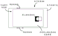
Fig. 1 is a block diagram of an example of a system 180 with a fingerprint sensing module 180 comprising a fingerprint sensor 181, which may be implemented as an optical fingerprint sensor comprising optical sensing based on fingerprints disclosed in this document. The system 180 includes a fingerprint sensor control circuit 184 and a digital processor 186. the digital processor 186 may include one or more processors for processing a fingerprint pattern and determining whether the input fingerprint pattern is that of an authorized user. The fingerprint sensing system 180 obtains a fingerprint using the fingerprint sensor 181 and compares the obtained fingerprint to a stored fingerprint to enable or disable functions in a device or system 188 protected by the fingerprint sensing system 180. In operation, the fingerprint processor 186 controls access to the device 188 based on whether the captured user fingerprint is from an authorized user. As shown, the fingerprint sensor 181 may include a plurality of fingerprint sensing pixels, e.g., pixels 182A-182E that collectively represent at least a portion of a fingerprint. For example, the fingerprint sensing system 180 may be implemented at an ATM as the system 188 to determine the fingerprint of a customer requesting access to funds or other transactions. Based on a comparison of the customer fingerprint obtained from the fingerprint sensor 181 with one or more stored fingerprints, the fingerprint sensing system 180 may cause the ATM system 188 to grant the requested access to the user account in response to a positive identification, or may deny the access in response to a negative identification. As another example, the device or system 188 may be a smartphone or portable device, and the fingerprint sensing system 180 is a module integrated into the device 188. As another example, the device or system 188 may be a door or a secure portal to a facility or home that uses the fingerprint sensor 181 to grant or deny access. As another example, the device or system 188 may be a car or other vehicle that is linked to the start of the engine using the fingerprint sensor 181 and identifies whether a person is authorized to operate the car or vehicle.
As a specific example, fig. 2A and 2B illustrate one exemplary implementation of an electronic device 200, the electronic device 200 having a touch-sensing display screen assembly and an optical fingerprint sensor module located below the touch-sensing display screen assembly. In this particular example, the display technology may be implemented by an LCD display screen having a backlight for optically illuminating LCD pixels or another display screen (e.g., an OLED display screen) having light-emitting display pixels without using a backlight. The electronic device 200 may be a portable device such as a smart phone or a tablet computer, or may be the device 188 shown in fig. 1.
Fig. 2A shows the front side of device 200, which is similar to some features in some existing smartphones or tablets. The device screen is located on the front of the device 200, occupying all, most, or a significant portion of the front space, and fingerprint sensing functionality is provided on the device screen, e.g., one or more sensing regions for receiving a finger on the device screen. As an example, fig. 2A shows a fingerprint sensing area for finger touch in a device screen that may be illuminated as a clearly identifiable region or area for a user to place a finger for fingerprint sensing. Such a fingerprint sensing area may be used to display images as the rest of the screen of the device. As shown, in various implementations, the device housing of device 200 may have a side that supports side control buttons that are common in various smartphones currently on the market. Also, as shown in one example of the upper left corner of the device housing in FIG. 2A, the device 200 may be provided with one or more optional sensors on the front side of the device outside the screen.
Fig. 2B shows an example of the structural configuration of the modules of the device 200 that are relevant to optical fingerprint sensing disclosed in this document. The device screen assembly shown in fig. 2B includes: for example, a touch-sensing screen module having a touch-sensing layer on top, and a display screen module having a display layer located below the touch-sensing screen module. An optical fingerprint sensor module is coupled to and below the display screen assembly module to receive and collect return light from the top surface of the touch sensing screen module and direct and image the return light onto an optical sensor array of optical sensing pixels or photodetectors that convert optical images in the return light into pixel signals for further processing. Below the optical fingerprint sensor module is a device electronics structure that contains certain electronic circuitry for the optical fingerprint sensor module and other components in the device 200. The device electronics may be disposed inside the device housing and may include components below the optical fingerprint sensor module as shown in fig. 2B.
In some implementations, the top surface of the device screen assembly can be a surface of an optically transparent layer that serves as a user touch sensing surface to provide a variety of functions, such as (1) a display output surface through which light carrying a display image passes to the eyes of a viewer, (2) a touch sensing interface that receives user touch by a touch sensing screen module for touch sensing operations, and (3) an optical interface for on-screen fingerprint sensing (and possibly one or more other optical sensing functions). The optically transparent layer may be a rigid or flexible layer such as a glass or crystalline layer.
One example of a display screen is an LCD display screen having LCD layers and a Thin Film Transistor (TFT) structure or substrate. The LCD display panel is a multi-layer Liquid Crystal Display (LCD) module that includes LCD display backlight light sources (e.g., LED lamps) that emit LCD illumination light for the LCD pixels, an optical waveguide layer that guides the backlight, and LCD structure layers that may include, for example, Liquid Crystal (LC) cell layers, LCD electrodes, transparent conductive ITO layers, optical polarizer layers, color filter layers, and touch sensing layers. The LCD module further includes a backlight diffuser located below the LCD structural layer and above the light guide layer for spatially dispersing backlight for illuminating LCD display pixels; and an optical reflector film layer below the light guide layer for recycling the backlight to the LCD structure layer to improve light utilization and display brightness. For optical sensing, one or more separate illumination sources may be provided and operated independently of the backlight sources of the LCD display module.
Referring to fig. 2B, the optical fingerprint sensor module in this example is located below the LCD display panel to collect return light from the top touch sensing surface and acquire a high resolution fingerprint pattern image when a user's finger is in contact with a sensing area on the top surface. In other implementations, the disclosed off-screen optical fingerprint sensor module for fingerprint sensing may be implemented on a device without touch sensing features.
Fig. 3A and 3B illustrate an example of a device implementing the optical fingerprint sensor module of fig. 2A and 2B. Fig. 3A illustrates a cross-sectional view of a portion of a device including an off-screen optical fingerprint sensor module. Fig. 3B shows a view of the front of a device with a touch-sensing display screen on the left, indicating a fingerprint sensing area on the lower portion of the screen, and a perspective view of a portion of the device including an optical fingerprint sensor module located below the device display screen assembly on the right. Fig. 3B also shows an example of a layout of a flexible strip with circuit elements.
In the design examples of fig. 2A-2B and 3A-3B, the optical fingerprint sensor design differs from some other fingerprint sensor designs that use a fingerprint sensor structure that is separate from the display screen and that have a physical interface between the display screen and the fingerprint sensor on the surface of the mobile device (e.g., button-like structures in the opening of the top glass cover plate in some mobile phone designs). In the design shown herein, the optical fingerprint sensor for detecting fingerprint sensing signals and other optical signals is located below the top cover glass or layer (e.g., fig. 3A), such that the top surface of the cover glass serves as the top surface of the mobile device as a continuous and uniform glass surface throughout the vertically stacked and vertically overlapping display screen layers and optical detection sensors. Examples of such designs for integrating optical fingerprint sensing and touch sensitive display screens under a common and uniform surface provide benefits including improved device integration, enhanced device packaging, enhanced device resistance to external elements, failure, wear and tear, and enhanced user experience during holding of the device.
Referring back to fig. 2A and 2B, the illustrated off-screen optical fingerprint sensor module for on-screen fingerprint sensing may be implemented in various configurations. In one implementation, a device based on the above design may be configured to include a device screen that provides touch sensing operations and includes an LCD display panel structure for forming a display image, the device further including a top transparent layer formed over the device screen as an interface to be touched by a user for touch sensing operations and to transmit light from the display structure to display an image to the user, the device further including an optical fingerprint sensor module located below the display panel structure to receive light returned from the top transparent layer to detect a fingerprint.
Such devices and other devices disclosed herein may also be configured to include various features. For example, a device electronic control module may be included in the device to grant the user access to the device when the detected fingerprint matches that of an authorized user. Further, the optical fingerprint sensor module is configured to detect, in addition to detecting the fingerprint, a biometric parameter other than the fingerprint by optical sensing to indicate whether a touch associated with the detected fingerprint at the top transparent layer is from a live person, and if (1) the detected fingerprint matches a fingerprint of an authorized user, and (2) the detected biometric parameter indicates that the detected fingerprint is from a live person, the device electronic control module is configured to grant the user access to the device. The biometric parameter may include, for example, whether the finger contains a person's blood flow or heartbeat.
For example, the device may include a device electronic control module coupled to the display panel structure to provide power to the light emitting display pixels and control image display of the display panel structure, and in a fingerprint sensing operation, the device electronic control module operates to turn off the light emitting display pixels in one frame and turn on the light emitting display pixels in a next frame to allow the optical sensor array to capture two fingerprint images with and without illumination of the light emitting display pixels, thereby reducing background light in fingerprint sensing.
As another example, the device electronic control module may be coupled to the display panel structure to provide power to the LCD display panel and to turn off backlight power to the LCD display panel in the sleep mode, and when the optical fingerprint sensor module detects the presence of the person's skin at the designated fingerprint sensing area of the top transparent layer, the device electronic control module may be configured to wake up the display panel structure from the sleep mode. More specifically, in some implementations, the device electronic control module may be configured to operate one or more illumination light sources in the optical fingerprint sensor module to intermittently emit light while turning off power to the LCD display panel (in a sleep mode) for directing the intermittently emitted illumination light to designated fingerprint sensing areas of the top transparent layer for monitoring the presence of human skin in contact with the designated fingerprint sensing areas for waking up the device from the sleep mode.
As another example, the device may include a device electronic control module coupled to the optical fingerprint sensor module to receive information of a plurality of detected fingerprints obtained by sensing a touch of a finger, and operative to measure a change in the plurality of detected fingerprints and determine a touch force causing the measured change. For example, the change may include a change in a fingerprint image due to a touch force, a change in a touch area due to a touch force, or a change in fingerprint ridge spacing.
As another example, the top transparent layer may include a designated fingerprint sensing area for a user to touch with a finger for fingerprint sensing, and the optical fingerprint sensor module below the display panel structure may include a transparent block in contact with the display panel substrate to receive light emitted from the display panel structure and returning from the top transparent layer, the optical fingerprint sensor module may further include an optical sensor array to receive the light, and an optical imaging module to image the light received in the transparent block onto the optical sensor array. The optical fingerprint sensor module may be positioned relative to a designated fingerprint sensing area and configured to: light returned by total internal reflection at the top surface of the top transparent layer is selectively received when in contact with the skin of the person, and light returned from the designated fingerprint sensing area is not received when there is no contact with the skin of the person.
As another example, an optical fingerprint sensor module may be configured to include an optical wedge positioned below a display panel structure to change a total reflection condition on a bottom surface of the display panel structure engaged with the optical wedge to allow light extracted from the display panel structure through the bottom surface, an optical sensor array to receive light extracted from the optical wedge from the display panel structure, and an optical imaging module positioned between the optical wedge and the optical sensor array to image light from the optical wedge onto the optical sensor array.
Fig. 4A and 4B illustrate an example of one implementation of an optical fingerprint sensor module located below a display screen assembly for implementing the design of fig. 2A and 2B. The device shown in fig. 4A and 4B includes a display assembly 423 having a top transparent layer 431 formed over the device screen assembly 423 as an interface that is touched by a user for touch sensing operations and transmits light from the display structure to display images to the user. In some implementations, the top transparent layer 431 may be a cover glass or a crystalline material. The device screen assembly 423 may include an LCD display module 433 below a top transparent layer 431. The LCD display layer allows partial optical transmission such that light from the top surface is partially transmitted through the LCD display layer to the optical fingerprint sensor module under the LCD. For example, the LCD display layer includes electrodes and wiring structures that optically function as an array of apertures and light scattering objects. A device circuitry module 435 may be disposed below the LCD display panel to control operation of the device and to perform functions for a user to operate the device.
The optical fingerprint sensor module 702 in this particular implementation example is located below the LCD display module 433. One or more illumination sources, such as an illumination source 436 under the LCD display module 433 or/and another one or more illumination sources under the top cover glass 431, are provided for providing illumination or detection light that is optically sensed by the optical fingerprint sensing module 702, and may be controlled to emit light to illuminate the fingerprint sensing region 615 on the top transparent layer 431 within the device screen area at least partially through the LCD display module 433 for a user to place a finger therein for fingerprint recognition. Illumination light from one or more illumination light sources 436 may be directed to the fingerprint sensing region 615 on the top surface as if the illumination light were from the fingerprint illumination light zone 613. Another one or more illumination sources may be located below the top cover glass 431 and may be placed adjacent the fingerprint sensing area 615 on the top surface to direct the generated illumination to the top cover glass 433 without passing through the LCD display module 433. In some designs, one or more illumination sources may be located above the bottom surface of the top cover glass 431 to direct the generated illumination to the fingerprint sensing area above the top surface of the top cover glass 433 without having to pass through the top cover glass 431, e.g., to directly illuminate a finger above the top cover glass 431.
As shown in fig. 4A, a finger 445 is placed in an illuminated fingerprint sensing region 615 as an active sensing region for fingerprint sensing. A portion of the light reflected or scattered in the region 615 is directed into the optical fingerprint sensor module below the LCD display module 433, and a photodetector sensing array within the optical fingerprint sensor module receives this light and collects fingerprint pattern information carried by the received light. The one or more illumination sources 436 are separate from the backlight source for the LCD display module and operate independently of the backlight source for the LCD display module.
In such designs that use one or more illumination light sources 436 to provide illumination light for optical fingerprint sensing, in some implementations, each illumination light source 436 may be controlled to turn on intermittently at a relatively slow period, thereby reducing the energy source for optical sensing operations. In some implementations, the fingerprint sensing operation can be implemented in a two-step process: first, one or more illumination light sources 436 are turned on in a flash mode without turning on the LCD display panel to sense whether a finger touches the sensing region 615 using blinking light, and then, once a touch is detected in the region 615, the optical sensing module is operated to perform fingerprint sensing based on optical sensing and the LCD display panel may be turned on.
In the example of fig. 4B, the underscreen optical fingerprint sensor module includes a transparent block 701 coupled to the display panel to receive return light from the top surface of the device assembly and an optical imaging block 702 to perform optical imaging and imaging acquisition. In one design of the illumination sources 436, the illumination sources 436 are positioned to direct illumination light first through the top cover glass 431 and then to the finger, from which light from one or more of the illumination sources 436 is reflected or scattered back after reaching the top cover surface, e.g., the top cover surface at the sensing area 615 where the user's finger is touching or otherwise not touching the top cover surface. When a fingerprint ridge is in contact with the top surface of the cover plate in the sensing area 615, the light reflection under the fingerprint ridge is different from the light reflection under the fingerprint valley at another location where no skin or tissue of the finger is present due to the presence of skin or tissue of the finger in contact at that location. Such a difference in light reflection conditions at the positions of ridges and valleys in the area touched by a finger on the top surface of the cover sheet forms an image representing the spatial distribution of ridges and valleys of the touched portion of the finger. The reflected light is directed back to the LCD display module 433 and, after passing through the aperture of the LCD display module 433, reaches the interface of the low index optically transparent block 701 of the optical fingerprint sensor module. The low-index optically transparent block 701 is configured to have a refractive index less than that of the LCD display panel so that the returning light can be extracted from the LCD display panel into the optically transparent block 701. Once the return light is received within the optically transparent block 701, this received light enters an optical imaging unit that is part of the imaging sensing block 702 and is imaged onto a photodetector sensing array or optical sensing array within the block 702. The difference in light reflection between the fingerprint ridges and valleys produces the contrast of the fingerprint image. As shown in fig. 4B, a control circuit 704 (e.g., a microcontroller or MCU) is coupled to the imaging sensing block 702 and other circuitry on the main circuit board, such as a device main processor 705.
In this particular example, the optical light path design is configured such that the illumination light enters the cover plate top surface over a range of total reflection angles on the top surface between the substrate and air interface, and therefore the reflected light is most efficiently collected by the imaging optics and imaging sensor array in block 702. In this design, the image of the fingerprint ridge/valley area exhibits maximum contrast due to the total internal reflection condition at each finger valley location where the finger tissue does not touch the top cover glass 431 top cover surface. Implementations of such imaging systems may have undesirable optical distortions that can adversely affect fingerprint sensing. Thus, the acquired image is further corrected by distortion correction during imaging reconstruction when processing the output signals of the optical sensor array in block 702 based on the optical distortion profile at the optical sensor array along the optical path of the returning light. By scanning the test image pattern of one row of pixels at a time across the sensing area of the X-direction lines and the Y-direction lines, distortion correction coefficients can be generated from the image acquired at each photodetector pixel. This correction process may also use images from turning on individual pixels one at a time and scanning the entire image area of the photodetector array. This correction factor only needs to be generated once after assembly of the sensor.
Ambient light from the environment (e.g., sunlight or indoor illumination) can enter the image sensor through the top surface of the LCD panel and then through the aperture in the LCD display assembly 433. Such background light may produce a background baseline in the valuable image from the finger and thus may undesirably reduce the contrast of the acquired image. Different approaches may be used to reduce this undesirable baseline intensity caused by background light. One example is to turn the illumination source 436 on and off at an illumination modulation frequency f, and by phase synchronizing the source drive pulses with the image sensor frame, the image sensor thus acquires the received image at the same illumination modulation frequency. In this operation, only one of the image phases contains light from the light source. In implementing this technique, the imaging acquisition can be timed to acquire images with illumination turned on at even (or odd) frames while the illumination is turned off at odd (or even) frames, so the even and odd frames can be subtracted for obtaining images formed primarily of light emitted by the modulated illumination source with significantly reduced background light. Based on this design, one frame of fingerprint signal is generated per display scan frame, and two consecutive signal frames are obtained by turning the illumination light on in one frame and off in the other frame. Subtraction of adjacent frames may be used to minimize or substantially reduce the effects of ambient background light. In some implementations, the fingerprint sensing frame rate may be half of the display frame rate.
In the example shown in fig. 4B, a portion of the light from the one or more illumination sources 436 may also pass through the cover top surface and into the finger tissue. This portion of the illumination light is scattered around, and a portion of this scattered light may eventually be collected by the imaging sensor array in the optical fingerprint sensor module 702. The intensity of this scattered light is a result of interaction with the internal tissue of the finger and therefore depends on the skin colour of the finger, the blood concentration in the finger tissue or the internal finger tissue. This information of the finger is carried by this scattered light on the finger, is useful for fingerprint sensing, and can be detected as part of the fingerprint sensing operation. For example, the intensity of the region of the user's finger image may be integrated at the time of detection to measure or observe an increase or decrease in blood concentration associated with or dependent on the phase of the user's heartbeat. Such features may be used to determine the heart rate of a user, to determine whether a user's finger is a live finger, or to provide a spoofing device with a counterfeit fingerprint pattern. The latter part of this patent document provides an additional example of information in light using internal tissue information carrying fingers.
In some designs, one or more of the illumination sources 436 in fig. 4B may be designed to emit illumination light of different colors or wavelengths, and the optical fingerprint sensor module may collect return light from the human finger at different colors or wavelengths. By recording the intensity of the corresponding measured return light at different colors or wavelengths, information associated with the user's skin tone, blood flow, or internal tissue structures within the finger may be measured or determined. For example, when a user registers a finger for fingerprint authentication operations, the optical fingerprint sensor may be operable to measure the intensity of scattered light from the finger at two different colors or wavelengths of illumination light associated with light color A and light color B, respectively, as intensities Ia and Ib. When a user's finger is placed on the sensing area on the top sensing surface to measure the fingerprint, the ratio of Ia/Ib can be recorded for comparison with later measurements. The method may be used as part of an anti-spoofing system for a device to reject spoofed devices made by using simulated user fingerprints or fingerprints that are the same as a user fingerprint but may not match a user's skin tone or other biometric information of the user.
One or more illumination sources 436 may be controlled by the same electronics 704 (e.g., MCU) used to control the image sensor array in block 702. The one or more illumination light sources 436 may be pulsed for short periods of time (e.g., low duty cycle) to intermittently emit light and provide pulsed light for image sensing. The image sensor array may be operable to monitor the light pattern at the same pulse duty cycle. If there is a human finger touching sensing area 615 on the screen, the image acquired at the imaging sensing array in block 702 may be used to detect a touch event. The control electronics or MCU 704 connected to the image sensor array in block 702 can operate to determine if the touch is a human finger touch. If a human finger touch event is determined, the MCU 704 may be operable to wake up the smartphone system, turn on one or more illumination sources 436 for optical fingerprint sensing, and acquire a complete fingerprint image using the normal mode. The image sensor array in block 702 sends the acquired fingerprint image to the smartphone host processor 705, and the smartphone host processor 705 may be operable to match the acquired fingerprint image to a registered fingerprint database. If there is a match, the smartphone unlocks the handset to allow the user to access the handset and initiate normal operations. And if the collected images are not matched, the smart phone feeds back the authentication failure to the user and keeps the locking state of the smart phone. The user may attempt to perform fingerprint sensing again or may enter a password as an alternative to unlocking the handset.
In the example shown in fig. 4A and 4B, the off-screen optical fingerprint sensor module uses an optically transparent block 701 and an imaging sensing block 702 having a photodetector sensing array to optically image a fingerprint pattern of a touching finger in contact with the top surface of the display screen onto the photodetector sensing array. By way of example, an optical imaging or detection axis 625 from sensing region 615 to the photodetector array in block 702 is shown in FIG. 4B. The optically transparent block 701 and the front end of the imaging sensing block 702 in front of the photodetector sensing array form a volume imaging module to enable suitable imaging for optical fingerprint sensing. Distortion correction can be used to achieve a desired imaging operation due to optical distortion in the imaging process.
In the optical sensing disclosed herein by the underscreen optical fingerprint sensor module in fig. 4A and 4B and other designs, the optical signal from the sensing region 615 on the top transparent layer 431 to the underscreen optical fingerprint sensor module includes different optical components.
Fig. 5A-5C illustrate signal generation for light returning from sensing region 615 under different optical conditions in order to understand the operation of the off-screen optical fingerprint sensor module. Light entering the finger from the illumination source or from other sources (e.g., background light) may produce internally scattered light in the tissue below the surface of the finger, such as scattered light 191 in fig. 5A-5C. This internally scattered light in the tissue below the finger surface may propagate through the internal tissue of the finger and then through the finger skin into the top transparent layer 431, carrying some information not carried by the light scattered, refracted or reflected by the finger surface, e.g., information about the color of the finger skin, blood concentration or flow characteristics within the finger, or the optical transmission pattern of the finger, which contains (1) a two-dimensional spatial pattern of external ridges and valleys of the fingerprint; and (2) an internal fingerprint pattern associated with an internal finger anatomy that produces the external ridges and valleys of the finger.
Fig. 5A shows an example of how illumination light from the one or more illumination light sources 436, after passing through the top transparent layer 431, propagates through the OLED display module 433 and generates different return light signals to the underscreen optical fingerprint sensor module, including light signals carrying fingerprint pattern information. For simplicity, the two illumination rays 80 and 82 at two different locations are directed to the top transparent layer 431 without undergoing total reflection at the interface of the top transparent layer 431. Specifically, illumination rays 80 and 82 are perpendicular or near perpendicular to top layer 431. Finger 60 is in contact with sensing region 615 on top transparent layer 431. As shown, the illumination beam 80, after passing through the top transparent layer 431, reaches the finger ridge in contact with the top transparent layer 431 to generate a beam 183 in the finger tissue and another beam 181 that returns to the LCD display module 433. The illuminating light beam 82, after passing through the top transparent layer 431, reaches the finger valley above the top transparent layer 431 to generate a reflected light beam 185 returning from the interface of the top transparent layer 431 to the LCD display module 433, a second light beam 189 entering the finger tissue, and a third light beam 187 reflected by the finger valley.
In the example of fig. 5A, it is assumed that the equivalent index of refraction of the finger skin at 550nm is about 1.44, and the cover glass index of refraction of the top transparent layer 431 is about 1.51. The finger ridge-cover glass interface reflects a portion of the light beam 80 as reflected light 181 to the bottom layer 524 below the LCD display module 433. In some LCD panels, the reflectivity may be low, for example, about 0.1%. Most of the light in beam 80 becomes transmitted through beam 183 in finger tissue 60, and finger tissue 60 causes scattering of light 183, producing scattered light 191 that returns to LCD display module 433 and bottom layer 524. Scattering of transmitted light beam 189 from LCD pixel 73 in the finger tissue also contributes to the returning scattered light 191.
The light beam 82 at the finger skin valley location 63 is reflected by the cover glass surface. In some designs, for example, the reflectance may be about 3.5% as the reflected light 185 is directed toward the underlayer 524, and the finger valley surface may reflect about 3.3% of the incident light energy (light 187) to the underlayer 524, such that total reflection may be about 6.8%. Most of the light 189 is transmitted into the finger tissue 60. A portion of the light energy in the transmitted light 189 in the finger tissue is scattered by the tissue, contributing to the scattered light 191 toward and into the bottom layer 524.
Thus, in the example of fig. 5A, the light reflections from the various interfaces or surfaces at the finger valleys and finger ridges of the touching finger are different, and this reflectance difference carries fingerprint map information and can be measured to extract the fingerprint pattern of the portion in contact with the top transparent layer 431 and illuminated by the OLED light.
Fig. 5B and 5C show the light paths of two additional types of illumination rays under different conditions and on the top surface at different positions with respect to the valleys or ridges of the finger, including the light paths of the illumination rays under total reflection conditions at the interface of the top transparent layer 431. The illustrated illumination light generates different return light signals to the underscreen optical fingerprint sensor module, including light signals carrying fingerprint pattern information. It is assumed that the cover glass 431 and the LCD display module 433 are bonded together without any air gap therebetween, so that illumination light having a large incident angle with respect to the cover glass 431 is totally reflected at the cover glass-air interface. Fig. 5A, 5B and 5C show examples of three different sets of diverging beams: (1) the central light beam 82, which has a small incident angle with respect to the cover glass 431 and does not undergo total reflection (fig. 5A), (2) the high-contrast light beams 201, 202, 211, and 212, which undergo total reflection at the cover glass 431 when no object touches the cover glass surface and can be coupled into finger tissue when a finger touches the cover glass 431 (fig. 5B and 5C), and (3) the escape light beams having a large incident angle, which undergo total reflection at the cover glass 431 even at the position where the finger tissue touches.
For the center beam 82, in some designs, the cover glass surface reflects about 0.1% to about 3.5% of the light to the beam 185, which is transmitted into the bottom layer 524, and the finger skin may reflect about 0.1% to about 3.3% of the light to the beam 187, which is also transmitted into the bottom layer 524. The difference in reflection depends on whether the light beam 82 meets the finger skin ridge 61 or valley 63. The remaining light beam 189 is coupled into finger tissue 60.
For high contrast light beams 201 and 202 that satisfy the condition of local total internal reflection, the cover glass surface reflects nearly 100% of the light to light beams 205 and 206, respectively, if no object touches the cover glass surface. When the finger skin ridge touches the cover glass surface and is located at the position of beams 201 and 202, most of the light energy can be coupled into finger tissue 60 through beams 203 and 204.
For high contrast light beams 211 and 212 satisfying the condition of local total internal reflection, the cover glass surface reflects almost 100% of the light to light beams 213 and 214, respectively, if no object touches the cover glass surface. When a finger touches the cover glass surface and the finger skin valley happens to be at the location of beams 211 and 212, no light energy is coupled into the finger tissue 60.
As shown in FIG. 5A, a portion of the illumination light coupled into the finger tissue 60 will be randomly scattered by the internal finger tissue to form low contrast light 191, and a portion of such low contrast light 191 will pass through the LCD display module 433 to the optical fingerprint sensor module. The portion of light collected by the optical fingerprint sensor module contains additional information about the finger's skin color, blood characteristics, and internal tissue structure of the finger associated with the fingerprint. Additional features for using internally scattered light in tissue below the surface of a finger in optical sensing will be explained in later sections of this patent document, such as obtaining an optically transmissive pattern of the finger, including (1) a two-dimensional spatial pattern of outer ridges and valleys of the fingerprint; and (2) an internal fingerprint pattern associated with an internal finger anatomy that produces the external ridges and valleys of the finger. Thus, in areas illuminated by the high contrast light beam, the finger skin ridges and valleys cause different optical reflections, and the reflection difference pattern carries fingerprint pattern information. High contrast fingerprint signals can be achieved by comparing such differences.
Based on the design shown in fig. 2A and 2B, the disclosed under-screen optical sensing technology can optically acquire fingerprints in various configurations. For example, the specific implementation of fig. 4B based on optical imaging using a volume imaging module of the optical sensing module may be implemented in various configurations.
Fig. 6A-6C illustrate an example of an off-screen optical fingerprint sensor module based on optical imaging via a lens for capturing a fingerprint from a finger 445 pressing against the display cover glass 423. Fig. 6C is an enlarged view of the optical fingerprint sensor module portion shown in fig. 6B. The off-screen optical sensor module shown in fig. 6B is located below the LCD display module 433 and includes: optically transparent spacers 617 bonded to the bottom surface of the LCD display module 433 for receiving return light from the sensing region 615 on the top surface of the top transparent layer 431; and an imaging lens 621 located between spacer 617 and photodetector array 623 to image received return light from sensing region 615 onto photodetector array 623. Unlike the example of the optical projection imaging system shown in fig. 4B, which does not include a lens, the example of the imaging design in fig. 6B uses an imaging lens 621 to capture a fingerprint image at a photodetector array 623 and image demagnification is achieved by the design of the imaging lens 621. To some extent similar to the imaging system in the example of fig. 4B, the imaging system for the optical fingerprint sensor module in fig. 6B may experience image distortion, and appropriate optical correction calibrations may be used to reduce such distortion, such as the distortion correction methods described for the system in fig. 4B.
Similar to the assumptions in fig. 5A-5C, assume that the equivalent refractive index of the finger skin at 550nm is about 1.44, and for the cover glass 423, the refractive index of the bare cover glass is about 1.51. When the OLED display module 433 is bonded on the cover glass 431 without any air gap, total internal reflection occurs at a large angle equal to or greater than the critical incident angle of the interface. The total reflection incident angle is about 41.8 ° if nothing touches the top surface of the cover glass, and about 73.7 ° if the finger skin touches the top surface of the cover glass. The corresponding difference in total reflection angle is about 31.9 °.
In this design, microlens 621 and photodiode array 623 define a viewing angle θ for capturing an image of a touching finger in sensing region 615. The viewing angle may be properly aligned by controlling a physical parameter or configuration in order to detect a desired portion of the sensing region 615 on the cover glass surface. For example, the viewing angle may be aligned to detect total internal reflection of the LCD display assembly. Specifically, the viewing angle θ is aligned to sense the active sensing region 615 on the cover glass surface. The effective sensing cover glass surface 615 may be viewed as a mirror such that the photodetector array effectively detects an image of the fingerprint illumination light zone 613 in the LCD display screen that is projected onto the photodetector array by the sensing cover glass surface 615. The photodiode/photodetector array 623 can receive the image reflected by the sensing cover glass surface 615 in region 613. When a finger touches sensing region 615, a portion of the light may couple into the ridge of the fingerprint, which causes the photodetector array to receive light from the ridge location to appear as a darker fingerprint image. Since the geometrical principles of the optical detection path are known, distortions of the fingerprint image caused in the optical path in the optical fingerprint sensor module can be corrected.
As a specific example, assume that the distance H from the center axis of the detection block to the top surface of the cover glass in FIG. 6B is 2 mm. This design may directly cover 5mm active sense area 615, where active sense area 615 is width Wc across the cover glass. Adjusting the thickness of spacers 617 may adjust detector position parameter H and may optimize effective sense region width Wc. Since H includes the thicknesses of the cover glass 431 and the display module 433, the application design should take these layers into account. The spacers 617, microlenses 621, and photodiode array 623 may be integrated under the color coating 619 on the bottom surface of the top transparent layer 431.
Fig. 7 illustrates an example of another design consideration for the optical imaging design of the optical fingerprint sensor module shown in fig. 6A-6C by using special spacers 618 instead of spacers 617 in fig. 6B-6C to increase the size of sensing region 615. The spacer 618 is designed to have a width Ws, a thickness Hs, and a low Refractive Index (RI) ns, and the spacer 618 is placed under the LCD display module 433, e.g., attached (e.g., adhered) to the bottom surface of the LCD display module 433. The end faces of the spacers 618 are angled or slanted faces that engage the microlenses 621. This relative position of the spacers and lenses is different from fig. 6B-6C, where the lenses are located below the spacers 617. The microlens 621 and the photodiode array 623 are assembled into an optical detection module having a detection angular extent θ. The detection axis 625 is bent due to optical refraction at the interface between the spacer 618 and the display module 433 and at the interface between the cover glass 431 and the air. The local angles of incidence φ 1 and φ 2 are determined by the refractive indices of the component materials RI, ns, nc, and na.
If nc is greater than ns, then φ 1 is greater than φ 2. Thereby, the sensing width Wc is magnified by refraction. For example, assuming that the equivalent refractive index RI of the finger skin is about 1.44 at 550nm and the refractive index RI of the cover glass is about 1.51, the total reflection incident angle is estimated to be about 41.8 ° if no object touches the top surface of the cover glass, and the total reflection angle is about 73.7 ° if the finger skin touches the top surface of the cover glass. The corresponding difference in total reflection angle is about 31.9 °. If the spacer 618 is made of the same material as the cover glass, the distance from the center of the detection module to the top surface of the cover glass is 2mm, and if the detection angle width θ is 31.9 °, the effective sensing area width Wc is about 5 mm. The corresponding local angle of incidence phi 1 phi 2 phi 57.75 deg. of the central axis. If the material of the special spacer 618 has a refractive index ns of about 1.4 and Hs of 1.2mm, the detection module is tilted at phi 1-70 deg.. The effective sensing area width is increased to above 6.5 mm. Under these parameters, the detection angle spread in the cover glass was reduced to 19 °. Accordingly, an imaging system for an optical fingerprint sensor module may be designed with the desire to enlarge the size of sensing region 615 on top transparent layer 431.
When the refractive index RI of a particular spacer 618 is designed to be sufficiently low (e.g., MgF is used)2、CaF2Or even air to form spacers), the width Wc of the active sensing region 615 is no longer limited by the thickness of the cover glass 431 and the display module 433. This property provides the desired design flexibility. In principle, the effective sensing area may even be increased to cover the entire display screen if the detection module has sufficient resolution.
Because the disclosed optical sensor technology can be used to provide a large sensing area to capture patterns, the disclosed underscreen optical fingerprint sensor module can be used to capture and detect not only patterns of fingers, but also patterns of larger sizes, such as a person's palm associated with a person, for user authentication.
Fig. 8A-8B illustrate an example of another design consideration for the optical imaging design of the optical fingerprint sensor module shown in fig. 7 by setting the opposing detection angle θ' of the photodetector array in the display screen surface and the distance L between the lens 621 and the spacer 618. Fig. 8A shows a cross-sectional view in a direction perpendicular to the surface of the display screen, and fig. 8B shows a view of the device as seen from the bottom or top of the display screen. A fill material 618c may be used to fill the space between the lens 621 and the photodetector array 623. For example, the fill material 618c may be the same material as the particular spacer 618 or another different material. In some designs, the filler material 618c may be an air space.
Fig. 9 shows another example of an underscreen optical fingerprint sensor module based on the design of fig. 7, wherein one or more illumination light sources 614 are disposed to illuminate a top surface sensing region 615 for optical fingerprint sensing. The illumination source 614 may be an extended type or a collimated type of light source such that all points within the active sensing region 615 are illuminated. The illumination source 614 may be a single element light source or an array of light sources.
10A-10B illustrate an example of an underscreen optical fingerprint sensor module using an optical coupler 628 shaped as a thin wedge to improve optical detection at an optical sensor array 623. Fig. 10A shows a cross-section of a device structure with an off-screen optical fingerprint sensor module for fingerprint sensing, and fig. 10B shows a top view of the device screen. An optical wedge 628 (having an index of refraction ns) is located below the display panel structure to alter the total reflection conditions at the bottom surface of the display panel structure that is engaged by the optical wedge 628, thereby allowing light to be extracted from the display panel structure through the bottom surface. An optical sensor array 623 receives light extracted from the display panel structure from the optical wedge 628, and an optical imaging module 621 is located between the optical wedge 628 and the optical sensor array 623 to image the light from the optical wedge 628 onto the optical sensor array 623. In the example shown, wedge 628 comprises a wedge surface that is tilted facing the optical imaging module and optical sensing array 623. In addition, as shown, there is a free space between wedge 628 and optical imaging module 621.
If the light is totally reflected at the sensing surface of the cover glass 431, the reflectivity is 100%, with the highest efficiency. However, if the light is parallel to the cover glass surface, the light will also be totally reflected at the LCD bottom surface 433 b. The wedge coupler 628 is used to change the local surface angle so that light can be coupled out for detection at the optical sensor array 623. The micro-holes in the LCD display module 433 provide a desired light propagation path so that light is transmitted through the LCD display module 433 for underscreen optical sensing. The actual light transmission efficiency may gradually decrease if the light transmission angle becomes too large or when the TFT layer becomes too thick. When the angle is close to the angle of total reflection, i.e., about 41.8 °, and the cover glass has a refractive index of 1.5, the fingerprint image looks good. Accordingly, the wedge angle of the wedge coupler 628 may be adjusted to several degrees, so that the detection efficiency may be improved or optimized. If the refractive index of the cover glass is selected to be higher, the total reflection angle becomes smaller. For example, if the cover glass is made of sapphire having a refractive index of about 1.76, the total reflection angle is about 34.62 °. The efficiency of transmission of detection light in the display screen is also improved. Therefore, this design uses a thin wedge to set the detection angle higher than the total reflection angle, and/or uses a cover glass material with a high refractive index, thereby improving detection efficiency.
In some underscreen optical fingerprint sensor module designs (e.g., the designs shown in fig. 6A-6C, 7, 8A, 8B, 9, 10A, and 10B), the sensing area 615 on the top transparent surface is not perpendicular or orthogonal to the detection axis 625 of the optical fingerprint sensor module, such that the image plane of the sensing area is also not perpendicular or perpendicular to the detection axis 625. Accordingly, the plane of the photodetector array 623 may be tilted with respect to the detection axis 625 to achieve high quality imaging at the photodetector array 623.
Fig. 11A-11C illustrate three example configurations for such tilting. FIG. 11A shows that sensing region 615a is tilted and not perpendicular to detection axis 625. In fig. 11B, sensing region 615B is aligned above detection axis 625 such that its image plane will also be located on detection axis 625. In practice, the lens 621 may be partially cut away to simplify packaging. In various implementations, the microlenses 621 can also be transmissive or reflective lenses. For example, a particular method is shown in FIG. 11C. Sensing region 615c is imaged by imaging mirror 621 a. The photodiode array 623b is aligned to detect a signal.
In the above-described design using lens 621, lens 621 may be designed to have an effective aperture that is larger than the aperture of the hole in the LCD display layer, thereby allowing light to be transmitted through the LCD display module for optical fingerprint sensing. Such a design may reduce the undesirable effects of wiring structures and other scattering objects in the LCD display module.
Fig. 12 shows an example of the operation of a fingerprint sensor for reducing or eliminating undesired contributions from background light in fingerprint sensing. The optical sensor array may be used to acquire various frames, and the acquired frames may be used to perform a difference and average operation between multiple frames to reduce the effects of background light. For example, in frame a, the illumination source for optical fingerprint sensing is turned on to illuminate the finger touch area, and in frame B, the illumination is changed or turned off. The subtraction of the signal of frame a and the signal of frame B may be used in image processing to reduce unwanted background light effects.
Unwanted background light in fingerprint sensing can also be reduced by providing suitable optical filtering in the light path. One or more optical filters may be used to filter ambient light wavelengths, e.g., near infrared IR light and portions of red light, etc. In some implementations, such optical filter coatings can be fabricated on surfaces of optical components, including the display screen bottom surface, the prism surface, or the sensor surface, among others. For example, a human finger may absorb most of the energy at wavelengths below about 580nm, and if one or more optical filters or optical filter coatings may be designed to reject light at wavelengths from 580nm to infrared, the undesirable contribution of ambient light to optical detection in fingerprint sensing may be greatly reduced.
FIG. 13 illustrates an example of an operational procedure for correcting image distortion in an optical fingerprint sensor module. At step 1301, one or more illumination sources are controlled and operated to emit light in a particular area, and the light emission of such pixels is modulated by the frequency F. At step 1302, an imaging sensor under a display panel is operated to acquire images at the same frequency F and at a certain frame rate. In the optical fingerprint sensing operation, a finger is placed on the top surface of the display panel cover substrate, and the finger modulates the light reflection intensity of the top surface of the display panel cover substrate. And an imaging sensor under the display screen collects the reflected light pattern after fingerprint modulation. At step 1303, the demodulation of the signal from the image sensor is synchronized at frequency F and background subtraction is performed. The resulting image reduces the effects of background light and includes the image resulting from the emission of light from the pixels. At step 1304, the acquired image is processed and calibrated to correct for image system distortion. At step 1305, the corrected image is used as a human fingerprint image for user authentication.
The same optical sensor used to collect the user's fingerprint can also be used to collect scattered light from the illuminated finger, such as the backscattered light 191 shown in FIG. 5A. The detector signals from the backscattered light 191 in fig. 5A in the region of interest can be integrated to produce an intensity signal. The intensity variation of the intensity signal is evaluated to determine other parameters than the fingerprint pattern, for example, the heart rate of the user or the internal topological organization of the finger associated with the external fingerprint pattern.
The above fingerprint sensor may be attacked by a malicious individual hacker who is able to obtain the fingerprint of an authorized user and copy the stolen fingerprint pattern on a carrier similar to a human finger. Such unauthorized fingerprint patterns may be used on a fingerprint sensor to unlock a target device. Thus, although a fingerprint pattern is a unique biometric identifier, it may not be a completely reliable or secure identification by itself. The off-screen optical fingerprint sensor module may also be used as an optical anti-spoofing sensor for sensing whether an input object having a fingerprint pattern is a finger from a live person and for determining whether the fingerprint input is a spoofing attack. This optical anti-spoofing sensing function is provided without the use of a separate optical sensor. Optical anti-spoofing can provide a high speed response without affecting the overall response speed of the fingerprint sensing operation.
FIG. 14 shows exemplary optical extinction coefficients for a material being monitored in blood, where the optical absorption is different between the visible spectral range of red light, e.g., 660nm, and the infrared range of infrared IR light, e.g., 940 nm. By illuminating the finger with probe light at a first visible wavelength (color a) and a second, different wavelength (color B), such as an Infrared (IR) wavelength, differences in optical absorption of the input object can be collected to determine whether the touch object is from a live human finger. One or more illumination light sources for providing optical sensing illumination may be used to emit light of different colors and as probe or illumination light of at least two different optical wavelengths for live finger detection with different optical absorption behavior of blood. When a person's heart beats, the pulse pressure pumps blood to flow in the artery, so the extinction ratio of the monitored material in the blood changes with the pulse. The received signal carries a pulse signal. These properties of blood can be used to detect whether the monitored material is a live or false fingerprint.
Fig. 15 shows a comparison between the behavior of optical signals in reflected light from an inanimate material (e.g., a fake finger or a spoof device having a fake fingerprint pattern) and a live finger. The optical fingerprint sensor may also operate as a heartbeat sensor to monitor a living subject. When detecting probe light at two or more wavelengths, the difference in extinction ratios can be used to quickly determine whether the monitored material is a living body, such as a living fingerprint. In the example shown in fig. 15, different wavelengths of probe light are used, one visible wavelength and the other infrared IR wavelength as shown in fig. 14.
When an inanimate material touches the top cover glass over the fingerprint sensor module, the received signal reveals an intensity level associated with the surface pattern of the inanimate material, and the received signal does not contain signal components associated with a live human finger. However, when a live person's finger touches the top cover glass, the received signal reveals signal characteristics associated with the live person, including significantly different intensity levels, due to the different extinction ratios at the different wavelengths. This method does not take a long time to determine whether the touch material is part of a living person. In fig. 15, the pulse-like signal reflects multiple touches, rather than blood pulsations. Similar multiple touches of inanimate material do not show differences caused by live fingers.
Such optical sensing of different optical absorption behavior of blood at different optical wavelengths may be performed in a short period for live finger detection and may be faster than optical detection of a person's heartbeat using the same optical sensor.
In the LCD display, the LCD backlight illumination is white light, containing light in the visible spectrum and infrared IR spectral ranges for performing the above-described live finger detection at the optical fingerprint sensor module. An LCD filter in the LCD display module may be used to allow the optical fingerprint sensor module to obtain the measurements in fig. 14 and 15. In addition, the prescribed light source 436 for generating optically sensed illumination light may be operated to emit detection light at selected visible and infrared IR wavelengths at different times, and the reflected detection light of two different wavelengths is collected by the optical detector array 623 to determine whether the touch object is a live finger based on the above-described operations shown in fig. 14 and 15. It is noted that although the reflected detection light of the selected visible and IR wavelengths may reflect different optical absorption characteristics of blood at different times, the fingerprint image is always acquired at different times by both the detection light of the selected visible wavelength and the detection light of the IR wavelength. Thus, fingerprint sensing can be done at both visible and IR wavelengths.
FIG. 16 shows an example of an operational procedure for determining whether an object in contact with an LCD display screen is part of a live human finger by operating one or more illumination sources for optical sensing to illuminate the finger with two different colors of light.
As another example, the disclosed optical sensor technology can be used to detect whether a captured or detected pattern of a fingerprint or palm is from a live human hand by a "live finger" detection mechanism through mechanisms other than the different optical absorption of blood at different optical wavelengths described above. For example, a living finger is typically moved or stretched due to natural movement or motion (intentional or unintentional) of a person, or is typically pulsed when blood flows through a body associated with a heartbeat. In one implementation, the optical fingerprint sensor module may detect changes in return light from the finger or palm due to heartbeat/blood flow changes, thereby detecting whether a live heartbeat is present in an object appearing as a finger or palm. User authentication may enhance access control based on a combination of optical sensing of a fingerprint/palm pattern and positive determination of the presence of a living person. As another example, when a person touches the LCD display screen, changes in the touch force may be reflected in one or more ways, including fingerprint pattern distortion, changes in the contact area between the finger and the screen surface, fingerprint ridge broadening, or blood flow dynamics changes. These and other variations can be measured by optical sensing based on the disclosed optical sensor technology and can be used to calculate touch force. Such touch force sensing may be used to add more functionality to the optical fingerprint sensor module than fingerprint sensing.
In the example of fingerprint pattern acquisition on an optical sensor array by an imaging module described above, optical distortion typically reduces image sensing fidelity, as shown in fig. 4B and 6B. This optical distortion can be corrected in various ways. For example, an optical image may be generated at the optical sensor array using a known pattern, and image coordinates in the known pattern may be correlated with the optical image generated at the optical sensor array with distortion for calibrating an imaging sensing signal output by the optical sensor array for fingerprint sensing. The fingerprint sensing module calibrates the output coordinates with reference to the image of the standard pattern.
Various implementations may be made for the disclosed optical fingerprint sensor module according to the disclosure in this patent document. For example, the display panel may be configured to: each pixel emits light and can be controlled individually; the display panel comprises an at least partially transparent substrate; and a substantially transparent cover substrate. The optical fingerprint sensor module is placed below the display panel for sensing an image formed on top of a surface of the display panel. The optical fingerprint sensor module may be used to sense an image formed by light emitted from the display panel pixels. The optical fingerprint sensor module may include a transparent block having a refractive index lower than that of the display panel substrate, an imaging sensor block having an imaging sensor array, and an optical imaging lens. In some implementations, the low refractive index block has a refractive index in a range of 1.35 to 1.46 or 1 to 1.35.
As another example, a method may be provided for fingerprint sensing, in which light emitted from a display panel is reflected by a cover substrate, and a finger on top of the cover substrate interacts with the light to modulate a light reflection pattern of a fingerprint. The imaging sensing module below the display panel is used for sensing the reflected light pattern image and reconstructing a fingerprint image. In one implementation, the emitted light from the display panel is modulated in the time domain, and the imaging sensor is synchronized with the modulation of the light-emitting pixels, where the demodulation process rejects most of the background light (future light from the target pixels).
As described above, the display screen of the portable electronic device is generally implemented as a component having multiple layers. For example, a display screen implemented as a touch screen may include a display layer for outputting video data, a capacitive touch screen layer for detecting touch events, a hard top layer, and so forth. The additional layer is used to integrate an off-screen optical sensing function, such as fingerprint sensing. To allow light to reach the sensing assembly, the light passes through the various layers between the top surface and the sensor (e.g., photodetector). To this end, the layers are designed to allow transmission of light, and some layers may be designed to enhance, bend, focus, collimate, reflect, and/or otherwise affect the transmission of light through the layers.
Fig. 17A and 17B show cross-sections of an illustrative portable electronic device 1700 and an illustrative display module 1710 for such a portable electronic device 1700, respectively, in accordance with various embodiments. Portable electronic device 1700 is shown as a smartphone. In other implementations, the portable electronic device 1700 is a laptop, a tablet, a wearable device, or any other suitable computing platform. Portable electronic device 1700 may include display system 423. As described above, the display system 423 may be a touch sensing display system 423. The display system 423 has integrated therein an off-screen optical sensor. As shown, the underscreen optical sensor may define a sensing region 615 within which optical sensing may be performed. For example, when a user places finger 445 on the display screen within sensing region 615, a fingerprint scan may be performed by the off-screen optical sensor. Such an underscreen optical sensor may be implemented using multiple layers.
Display module 1710 of fig. 17B may be one implementation of display system 423 of fig. 17A. As shown, the display module 1710 includes a plurality of layers. The top cover plate layer 1715 (e.g., glass) may serve as a user interface surface for various user interface operations. For example, the cover sheet layer 1715 may facilitate touch sensing operations by a user, display images to a user, serve as an optical sensing interface to receive fingers for optical fingerprint sensing and other optical sensing operations, and so forth. In some embodiments, display module 1710 includes a cover layer 1715. In other implementations, the cover layer 1715 is separate from the display module 1710. For example, the display module 1710 is integrated into the portable electronic device 1700 as a module, and the cover plate layer 1715 is mounted on top of the display module 1710.
One or more other layers of the display module 1710 form a Liquid Crystal Module (LCM) 1720. Below LCM 1720, display module 1710 includes enhancement layer 1725. As described herein, the enhancement layer 1725 can include one or more layers of brightness enhancement films, such as enhancement films including trapezoidal prism structures. Display module 1710 may also include some or all of light diffuser 1730, light guide plate 1735, reflector film 1740, and frame 1745. Additional components, such as one or more display light sources 1750, and one or more external light sources 1760 (e.g., for fingerprint sensing and/or other optical sensing) are included in some embodiments.
Implementations of display light source 1750 may include an LCD display screen backlight light source (e.g., an LED lamp) that provides white backlight for display module 1710. Implementations of light guide plate 1735 include a waveguide optically coupled with display light source 1750 to receive and guide backlight. Implementations of the LCM 1720 include some or all of a Liquid Crystal (LC) cell layer, LCD electrodes, a transparent conductive ITO layer, an optical polarizer layer, a color filter layer, a touch sensing layer, and the like. Implementations of the light diffuser 1730 include a backlight diffuser placed below the LCM 1720 and above the light guide plate 1735 to spatially disperse the backlight to illuminate the LCD display pixels in the LCM 1720. A reflector film 1740 is implemented to be placed under the light guide plate 1735 to recycle the backlight to the LCM 1720, thereby improving light utilization efficiency and display brightness.
When the LCD cell is turned on (e.g., in sensing region 615), the LCM 1720 (e.g., LC cell, electrode, transparent ITO, polarizer, color filter, touch sensing layer, etc.) may become partially transparent, although the microstructures may interfere with and/or block some of the detected light energy. Embodiments of the light diffuser 1730, light guide plate 1735, reflector film 1740, and frame 1745 are processed to secure the fingerprint sensor and provide a transparent or partially transparent sensing light path so that a portion of the reflected light from the top surface of the cover plate layer 1715 can reach the sensing elements (e.g., photodetector array) of the underscreen optical sensor. The underscreen optical sensor may include any suitable components, such as a fingerprint sensor component, a photodetector array, an optical collimator array for collimating and directing reflected probe light to the photodetector array, and an optical sensor circuit that receives and conditions detector output signals from the photodetector array. Embodiments of the photodetector array include a CMOS sensor comprised of CMOS sensing pixels, a CCD sensor array, or any other suitable optical sensor array.
Embodiments of the reinforcement layer 1725 include one or more reinforcement films. Some enhancement film designs include prismatic films having sharp prismatic ridge and sharp prismatic valley profiles (i.e., sharp transitions at each ridge and sharp transitions at each valley). For example, fig. 18A-18C show views of an illustrative portion of a symmetric enhancement layer 1800. Fig. 18A shows an enlarged view 1810 of a small portion of the symmetric enhancement layer 1800. Fig. 18B and 18C show cross-sections of a small portion of one reinforcement film layer 1820 of the symmetric reinforcement layer 1800. Fig. 18C shows a cross-section of a small portion of two reinforcement film layers 1820a, 1820b stacked in orthogonal directions relative to each other in a symmetric reinforcement layer 1800.
As shown, each enhancement film layer 1820 is formed with a series of sharp prismatic structures. Each sharp prism structure includes a sharp ridge 1822 and a sharp valley 1824. The enlarged view 1810 of fig. 18A shows the two reinforcement film layers 1820 of fig. 18C stacked in orthogonal directions relative to each other, as viewed from the top. As shown, the intersecting sharp prism structures form a grid of sharp ridge lines 1812 and sharp valley lines 1814, corresponding to the sharp ridge 1822 and sharp valley 1824, respectively, of each sharp prism structure. As shown in fig. 18C, the sharp ridge 1822 points in the direction of the LCM 1720.
Such enhancement layers 1800 typically attempt to enhance the brightness of light directed toward the viewer (e.g., toward and/or through LCM 1720). For example, the enhancement layer 1800 attempts to enhance the brightness of the backlight located behind the LCM 1720 and/or the brightness of the probe illumination for the off-screen optical sensing. As shown in fig. 18B, light passing through the prism structures of the enhancement layer 1800 is bent in different directions as shown by light paths 1832a and 1832B. Each light path 1832 shows two directions of propagation of light energy. The first direction (i.e., generally toward the LCM 1720) may represent a vector of backlight and/or probe illumination energy originating from a light source below the enhancement layer 1800. The second direction (i.e., generally away from the LCM 1720) may represent a vector of backlight and/or detected illumination energy that reflects off another layer (e.g., the top transparent layer above the LCM 1720) and propagates back along the direction of the below-screen optical sensor.
This bending may tend to be beneficial as light passes through the reinforcement film layer 1820 in the direction of the LCM 1720. For example, light passing through enhancement film layer 1820 in a first direction, including light paths with large incident angles (e.g., path 1832), may bend in a generally converging manner toward LCM 1720, thereby causing brightness enhancement. As a corollary, light passing through the enhancement layer 1800 in the second direction may tend to bend in a generally divergent manner. If optical sensing is attempted, image blurring may result. In typical display applications, this blurring is insignificant because the blurred light is entering the device and not directed towards the viewer. However, as described herein, in the context of off-screen optical fingerprint sensing, such blurring affects light propagating in the direction of the optical sensing component, which can hinder optical sensing by components below the conventional enhancement layer 1800.
For greater clarity, fig. 18B illustrates three exemplary potential reference positions (e.g., positions and orientations) 1850 for optical sensing. If an optical sensor is placed according to the reference position 1850a, the optical sensor may tend to detect light entering the enhancement film layers 1820 through the left and right prism faces, which may tend to cause image blur. However, if the optical sensor is placed according to reference position 1850b or 1850c, the optical sensor may tend to detect light entering the enhancement film layer 1820 only through the right or left prism face, respectively. In this case, blurring may be avoided, but at least half of the detection area may not be imaged.
Fig. 19A-19C show views of an illustrative portion of an asymmetric reinforcement layer 1900 according to various embodiments. The asymmetric enhancement layer 1900 may be another embodiment of the enhancement layer 1725. Fig. 19A shows an enlarged view 1910 of a small portion of an asymmetric reinforcement layer 1900. Fig. 19B shows a cross-section of a small portion of one enhancement film layer 1920 of the asymmetric enhancement layer 1900. Fig. 19C shows a cross-section of a small portion of two asymmetric layers 1920a, 1920b stacked in orthogonal directions relative to each other in an asymmetric reinforcement layer 1900.
As shown, each enhancement film layer 1920 is formed with a series of asymmetric prismatic structures. Each asymmetric prismatic structure (microprismatic structure) is generally defined by a cross-section having two angled sides, forming sharp ridges 1922 and sharp valleys 1924. As shown, each of the two angled sides is inclined at a respective different angle of inclination 1926 relative to the vertical. Notably, at each limit of the range of possible tilt angles 1926 is an embodiment in which one tilt angle 1926 is substantially zero degrees to effectively form a saw tooth ridge prism structure. In another embodiment, one oblique angle 1926 is 45 degrees and the other is 52 degrees. In another embodiment, one oblique angle 1926 is 45 degrees and the other is 54 degrees. In another embodiment, one oblique angle 1926 is 45 degrees and the other is 56 degrees. In another embodiment, one oblique angle 1926 is 38 degrees and the other is 52 degrees. In another embodiment, one oblique angle 1926 is 36 degrees and the other is 54 degrees. As described herein, the tilt angle 1926 is selected to provide a desired type and/or amount of brightness enhancement (e.g., for backlighting through the enhancement film layer 1920 in the direction of the LCM 1720).
The enlarged view 1910 of fig. 19A shows the two reinforcement film layers 1920 of fig. 19C stacked in orthogonal directions relative to each other, as viewed from the top. As shown, the intersecting prismatic structures form a grid of sharp ridge lines 1912 and sharp valley lines 1914, corresponding to the sharp ridges 1922 and sharp valleys 1924, respectively, of each sharp prismatic structure. This arrangement makes the top view look similar to the top view of the reinforcement layer 1800 of fig. 18, but provides various features that are different from the conventional reinforcement layer 1800.
Fig. 19B shows light propagating through the enhancement film layer 1920 in the direction of the LCM 1720, e.g., along light path 1930. Light that passes through the enhancement film layer 1920 generally in the direction of the LCM 1720 (i.e., having an upward directional component with reference to the illustrated direction), for example, those along the light paths 1930a and 1930b, is bent toward the perpendicular direction by the angled surfaces of the microprism structures. Thus, the asymmetric enhancement film layer 1920 provides backlight enhancement features, although some of the light paths are affected differently by the asymmetric prism structures than by the microprism structures of the symmetric enhancement layer 1800.
Unlike the symmetric enhancement layer 1800, the asymmetric enhancement film layer 1920 produces less blurring for light propagating in the opposite direction to the LCM 1720 (i.e., having a downward directional component with respect to the illustrated direction). Fig. 19B shows light propagating through enhancement film layer 1920 in such a direction (e.g., the direction of the underscreen optical sensor), for example, along optical path 1940. As shown, three objects 1950 are located at different positions relative to the asymmetric reinforced film layer 1920. For example, the object 1950 is a fingerprint ridge or valley of a finger placed on a fingerprint sensing area of a device having an asymmetric reinforced film layer 1920 disposed between the LCM 1720 and the under-screen optical fingerprint sensor. Light from the second object 1950B travels along a refracted light path 1940a to detection point "B" 1955B (e.g., corresponding to a first potential sensor location), while light from the third object 1950C travels along a refracted light path 1940B to detection point "C" 1955C (e.g., corresponding to a second potential sensor location). It is noted that although the objects 1950b and 1950c are relatively close, their respective detection points 1955b and 1955c are relatively far apart. After exiting the asymmetric enhancement film layer 1920 in a substantially vertical direction, light from the first object 1950a propagates along refracted light path 1945 to detection point "A" 1955 a. It can be seen that by configuring the sensor to detect light exiting along path 1945 (e.g., at detection location 1955 a), relatively clear and bright detection information can be produced. This is further illustrated in fig. 19C, where two stacked asymmetric enhancement film layers 1920 (in orthogonal directions relative to each other) can provide a clear image light path, such as represented by detection point 1955 a.
Additionally, as discussed above with reference to fig. 18A-18C, avoiding ambiguity may involve positioning the optical sensor to receive from only one of the left or right sides of the microprism structure. For example, a single optical sensor may be directed to detect object 1950a and object 1950b through paths 1945 and 1940a, respectively, because both of these optical paths reach the sensor through the right prism face. Furthermore, receiving optical information from only one face of the microprism structure can effectively reduce the sensing area that can be actually and accurately imaged without blurring.
For purposes of illustration, fig. 20 shows an illustrative fingerprint sensing region 615 overlaid on a single enhancement film layer 2000, such as enhancement film layers 1820 or 1920. As shown, the microprismatic structures of the enhancement film layer 2000 form parallel ridges that extend generally in a first direction (labeled "X" axis 2020) and generally orthogonal to a second direction (labeled "Y" axis 2025). Although not shown, it may be assumed that the "Z" axis points outward from the page in the direction of the LCM 1720, orthogonal to both the X and Y axes. As described above, although the theoretical fingerprint sensing area 615 occupies a relatively large sensing area, an optical sensor oriented to sense the entire area may tend to receive reflected probe light from both prism faces of each microprism structure, resulting in image blur. An optical sensor oriented to receive reflected probe light from only one prism face of each microprism structure can tend to avoid image blur, but also tends to result in a reduced sensing area (as shown in sensing subregion 2010). For example, the optical sensor may be oriented to point generally in the negative Y direction, the positive Z direction (e.g., {0, -Y, Z }). In this case, the actual sensing sub-region 2010 may be about half the area of the theoretical sensing region 615 or less.
Fig. 21 shows an illustrative fingerprint sensing area 615 overlaid on an enhanced panel 2100 having two enhanced film layers stacked such that their respective microprismatic structures extend in substantially orthogonal directions. The reinforced panel 2100 may be implemented as, for example, a reinforced panel as shown in fig. 18A and 19A or a pair of reinforced film layers as shown in fig. 18C and 19C. As shown, the enhanced panel 2100 has first microprism structures (e.g., of a first enhancement film layer) forming parallel ridges extending generally in a first direction (along an "X" axis 2020) and second microprism structures (e.g., of a second enhancement film layer) forming parallel ridges extending generally in a first two directions (along a "Y" axis 2025). With two enhancement film layers, each layer may cause haze. For example, light passing through one prism face of the microstructures of the lower enhancement film layer is a combination of light passing through both prism faces of the microstructures of the upper enhancement film layer. Thus, to avoid blurring, the optical sensor is oriented to receive reflected probe light from only one prism face of each microprism structure through the two enhancement film layers. For example, the optical sensor may be oriented to point generally in the positive X, negative Y, positive Z directions (e.g., { X, -Y, Z }). In this case, the actual sensing sub-region 2110 may be about one-quarter of the area of the theoretical sensing region 615. For example, when symmetric microprism structures (e.g., those shown in fig. 18A-18C) are used, the actual sensing sub-region 2110 may be less than one-fourth of the area of the theoretical sensing region 615, whereas when carefully designed asymmetric microprism structures (e.g., those shown in fig. 19A-19C) are used, the actual sensing sub-region 2110 may be slightly greater than one-fourth of the area of the theoretical sensing region 615.
Increasing the area of theoretical sense region 615 may offset the limitation of actual sense sub-region 2110 that is reduced in area. For example, doubling the area of theoretical sense region 615 may double the area of actual sense subregion 2110. One way to increase the area of the theoretical sensing region 615 is to increase the distance between the object being detected (e.g., a fingerprint feature) and the lens at the input of the optical sensor. However, directly increasing this distance may involve increasing the thickness of the optical sensor, which may be impractical in many applications. For example, in smartphone applications, it is desirable to maintain a thin package while still achieving a large sensing area. Some embodiments attempt to effectively increase the theoretical sensing area 615 by using refraction and reflection to create a folded optical path without a corresponding increase in sensor thickness.
Fig. 22 shows an illustrative underscreen optically-sensed environment 2200 in accordance with various embodiments. As shown, environment 2200 includes an underscreen optical sensing system disposed below display module 1710. The optical sensing system includes an optical sensing module 2210, a refractive structure 2220, and a reflective structure 2230. Optical sensing module 2210 may include any suitable components for optical sensing. For simplicity, the optical sensing module 2210 is shown as an optical detector 2212 and a lens 2214. For reference, display module 1710 is shown as defining a display plane 2205. For example, the display surface of display module 1710 is generally flat (e.g., although it may include a framed edge, a rounded edge, etc.) such that the display surface generally lies in the display plane 2205. Display module 1710 may be any suitable type of display screen and may include one or more layers. In some embodiments, as described above, display module 1710 is a Liquid Crystal Display (LCD) module having multiple layers including LCD layers (e.g., including an array of LCD pixels, electrode interconnects, etc.).
The optical sensing module 2210 is configured to obtain optical information from the received illumination energy. For example, as light enters the optical sensing module 2210 through the input aperture 2216, the light is focused by the lens 2214 onto the optical detector 2212, which optical detector 2212 may include an array of photodetectors and/or any other suitable component. The received illumination energy may then be converted into optical information. For example, the conversion may include any suitable optical processing (e.g., with lenses, filters, modulators, masks, etc.) and/or any suitable logical processing (e.g., using a computing processor, state machine, software, etc.). As shown, the input aperture 2216 may be oriented substantially parallel to the display plane 2205. In this configuration, the optical path that travels parallel to the display plane 2205 may enter the center of the input aperture 2216 coaxially with the lens 2214.
Reflective structure 2230 may receive reflected probe light that passes through display module 1710 (e.g., within optical sensing region 615) and may. In some embodiments, reflective structure 2230 includes a mirror integrated with (e.g., affixed to) top reflective surface 2235. For example, reflective structure 2230 includes structures that support and orient mirrors at appropriate angles for redirecting the optical path 2240 of reflected probe light toward refractive structure 2220. In other embodiments, the reflective structure 2230 is a monolithic prism body having an angled top surface 2235. In such embodiments, the integral prism bodies can be made of a material (e.g., plastic, glass, etc.) having a refractive index selected such that reflected probe light incident on the angled top surface 2235 after passing through the display module 1710 is reflected toward the refractive structure 2220. As shown, reflective structure 2230 is sized and oriented to redirect optical path 2240 of reflected probe light from the entire optical sensing region 615 to refractive structure 2220. In certain implementations, reflective structure 2230 is sized and oriented to redirect optical path 2240 of reflected probe light from only a portion of optical sensing region 615 and/or otherwise from a region outside of optical sensing region 615.
Embodiments of refractive structure 2220 receive reflected probe light from reflective structure 2230 and bend the optical path 2240 of the reflected probe light to converge on the input aperture 2216 of optical sensing module 2210. For example, as shown, light paths 2240a, 2240b, and 2240c originate from the leftmost edge, center, and rightmost edge, respectively, of optical sensing region 615, representing light path 2240 from the entire optical sensing region 615. Despite covering the larger optical sensing area 615, the light paths 2240 are all redirected by the reflective structures 2230 to the refractive structures 2220, and all are bent by the refractive structures 2220 to converge on the input aperture 2216 of the optical sensing module 2210. In some embodiments, the refractive structure 2220 is a monolithic prism body having a first refractive surface (e.g., farther from the optical sensing module 2210) to receive the reflected probe light from the reflective structure and a second refractive surface (e.g., closer to the optical sensing module 2210) to transmit the reflected probe light to the input aperture of the optical sensing module, the first refractive surface being at an angle relative to the second refractive surface. For example, as shown, the second refractive surface may be oriented substantially orthogonal to the display plane.
As described above (although not shown in fig. 22), embodiments may include an illumination source and a top transparent layer. An illumination source may be disposed below display module 1710 to generate probe light and direct the probe light through at least a portion of display module 1710. For example, the detection light source may include a Light Emitting Diode (LED), a Vertical Cavity Surface Emitting Laser (VCSEL), or any other suitable light source. A top transparent layer may be disposed over display module 1710 and configured as an output interface for images produced by display module 1710. In some implementations, the display module 1710 also includes touch sensitive features, and the top transparent layer can also be configured as an input interface for touch sensitive interaction. Although the optical sensing region 615 is shown as being substantially located in the display plane 2205, the optical sensing region 615 may also be defined with reference to the top surface of the top transparent layer. For example, when optical sensing module 2210 is configured for underscreen optical fingerprint sensing, a fingerprint is typically placed on the top surface of the top transparent layer such that optical sensing area 615 more directly corresponds to the area in the top surface of the top transparent layer where optical fingerprint sensing may be performed. Optical sensing region 615 may then be a region configured to receive probe light from an illumination source and reflect a portion of the probe light in response to an interaction between an object (e.g., a fingerprint feature) and the top surface. For example, as described above, the top transparent layer may be made of a material (e.g., treated glass) having a particular index of refraction relative to the air and/or fingerprint features or other objects above the top transparent layer. Thus, the probe light will tend to be reflected or not reflected at the top surface of the top transparent layer based on the presence of an object (e.g., fingerprint ridges will cause the probe light to be reflected, while fingerprint valleys will cause the probe light to be absorbed, scattered, etc.). In such embodiments, the reflected probe light redirected by reflective structures 2230, curved refractive structures 2220, and received by optical sensing module 2210 is probe light reflected by the top surface of the top transparent layer.
In some embodiments, reflective structure 2230 and refractive structure 2220 are configured (e.g., sized, shaped, positioned, and oriented) such that one of light paths 2240b that passes through the center of optical sensing region 615 is redirected by reflective structure 2230 and bent by refractive structure 2220 to enter the center of input aperture 2216 of the optical sensing module. For example, lens 2214 is a convex lens with a primary optical axis, and input aperture 2216 is aligned with lens 2214 such that the center of input aperture 2216 is aligned with the primary optical axis of lens 2214. In some embodiments, as shown, the reflective structures 2230 and the refractive structures 2220 are configured such that one of the light paths 2240b through the display module in a first direction substantially perpendicular to the display plane (e.g., perpendicular with respect to the illustration) is redirected by the reflective structures 2230 and bent by the refractive structures 2220 to enter the input aperture 2216 of the optical sensing module 2210 in a second direction substantially parallel to the display plane (e.g., horizontal with respect to the illustration).
Fig. 23 shows an illustrative underscreen optical sensing environment 2300 with off-axis sensing, in accordance with various embodiments. Similar to environment 2200 of fig. 22, environment 2300 includes an underscreen optical sensing system disposed below display module 1710. The optical sensing system includes an optical sensing module 2210, a refractive structure 2220, and a reflective structure 2230 (having a reflective top surface 2235). The optical sensing module 2210 may include any suitable components for optical sensing, such as an optical detector 2212 and a lens 2214. Unlike FIG. 22, the environment 2300 of FIG. 23 shows an actual optical sensing sub-region 2310 that is smaller than the theoretical optical sensing region 615, such as described with reference to FIGS. 20 and 21.
As described above, embodiments of display module 1710 may include an enhancement layer having a microprism structure. For example, each microprismatic structure can have at least first and second prism faces, and the first and second prism faces can be symmetric or asymmetric with respect to one another. As the reflected probe light passes through the microprism structure, some of the reflected probe light passes through a first prism face of the microprism structure and some of the reflected probe light passes through a second prism face of the microprism structure. For example, a first portion of the optical path 2340 of reflected probe light passes through a first prism face of the microprism structure and a second portion of the optical path 2340 of reflected probe light passes through a second prism face of the microprism structure such that the first and second portions of the optical path 2340 diverge. As described above, if the optical sensing module 2210 receives both the first and second portions of the optical path 2340, this divergence may cause blurring. Rather, embodiments may configure the optical sensing module 2210 to obtain optical information from the received illumination energy corresponding to only the first portion of the optical path 2340 of the reflected probe light. Thus, the actual optical sensing sub-region 2310 is smaller than the theoretical optical sensing region 615 (e.g., about half or a quarter of the area).
In some such embodiments, the enhancement layer includes a first enhancement film layer and a second enhancement film layer. The first enhancement film layer has first portions of microprismatic structures arranged to form first parallel prismatic ridges extending in a first direction and the second enhancement film layer has second portions of microprismatic structures arranged to form second parallel prismatic ridges extending in a second direction different from the first direction. For example, as shown in fig. 21, the first enhancement film layer may be substantially identical to the second enhancement film layer, and the first enhancement film layer may be stacked on top of the second enhancement film layer and oriented such that the first direction is orthogonal to the second direction. In some such embodiments, a first portion of the optical path 2340 of the reflected probe light passes through the first prism face of the first portion of the microprism structure and the first prism face of the second portion of the microprism structure, thereby passing through the first prism face of the microprism structure; a second portion of the optical path 2340 of reflected probe light passes through the second prism face of the first portion of the microprism structure and the second prism face of the second portion of the microprism structure, thereby passing through the second prism face of the microprism structure. There may also be a third portion of the optical path 2340 of reflected probe light and a fourth portion of the optical path 2340 of reflected probe light, the third portion passing through the first prism face of the first portion of the microprism structure and the second prism face of the second portion of the microprism structure and the fourth portion passing through the second prism face of the first portion of the microprism structure and the first prism face of the second portion of the microprism structure. Further, in such embodiments, the actual optical sensing sub-region 2310 may be smaller than the theoretical optical sensing region 615 (e.g., only about one-quarter of the theoretical optical sensing region 615 may be available without ambiguity).
An embodiment of the optical sensing module 2210 includes a lens 2214 and an optical detector 2212 (e.g., including any suitable type of sensing assembly) oriented such that reflected probe light converging on an input aperture 2216 of the optical sensing module 2210 is focused through the lens 2214 onto the optical detector 2212. Some such embodiments may be configured to preferentially select a first portion of the light path 2340 corresponding to illumination energy passing only (or primarily) through a particular face of the microprism structure (e.g., only the first prism face). For example, as shown in FIG. 23, the off-screen optical sensing system is configured such that light path 2340a and light path 2340b are directed into optical sensing module 2210 through reflective structure 2230 and refractive structure 2220, while light path 234c is not directed. In some such embodiments, the optical detector 2212 may be positioned off-axis relative to the lens in accordance with the general off-center light path resulting from the configuration preference of the first portion of the light path 2340 only. Thus, the optical detector 2212 can be configured (e.g., positioned and/or sized) to receive illumination energy reflected from the actual optical sensing sub-region 2310 rather than from the rest of the theoretical optical sensing region 615.
While this disclosure contains many specifics, these should not be construed as limitations on the scope of any application or claim, but rather as descriptions of features that may be specific to particular embodiments of a particular application. Certain features that are described in this patent document in the context of separate embodiments can also be implemented in combination in a single embodiment. Conversely, various features that are described in the context of a single embodiment can also be implemented in multiple embodiments separately or in any suitable subcombination. In addition, although features may be described above as acting in certain combinations and even initially claimed as such, one or more features from a claimed combination can in some cases be excised from the combination, and the claimed combination may be directed to a subcombination or variation of a subcombination.
Similarly, while operations are depicted in the drawings in a particular order, this should not be understood as requiring that such operations be performed in the particular order shown or in sequential order, or that all illustrated operations be performed, to achieve desirable results. Moreover, the separation of various system components in the embodiments described in this patent document should not be understood as requiring such separation in all embodiments.
Only a few implementations and examples have been described and other implementations, enhancements and variations can be made based on what is described and illustrated in this patent document.
Unless specifically stated to the contrary, reference to "a", "an" or "the" is intended to mean "one or more". Ranges may be expressed herein as from "about" one specified value, and/or to "about" another specified value. The term "about" is used herein to mean approximately, near, about, or left-to-right. When the term "about" is used in conjunction with a numerical range, it modifies that range by extending the upper and lower bounds of the numerical values set forth. In general, the term "about" is used herein to modify a numerical value above and below the stated value by a variance of 10%. When such a range is expressed, another embodiment includes from the one specified value and/or to the other specified value. Similarly, when values are expressed as approximations, by use of the antecedent "about," it will be understood that the particular value forms another embodiment. It is also understood that the endpoints of each of the ranges are inclusive of the range.
All patents, patent applications, publications, and descriptions mentioned herein are incorporated by reference in their entirety for all purposes. All of which are not considered prior art.