CN114242729A - Three-dimensional memory element - Google Patents
Three-dimensional memory element Download PDFInfo
- Publication number
- CN114242729A CN114242729A CN202010940210.4A CN202010940210A CN114242729A CN 114242729 A CN114242729 A CN 114242729A CN 202010940210 A CN202010940210 A CN 202010940210A CN 114242729 A CN114242729 A CN 114242729A
- Authority
- CN
- China
- Prior art keywords
- layer
- dimensional memory
- charge storage
- channel
- control gate
- Prior art date
- Legal status (The legal status is an assumption and is not a legal conclusion. Google has not performed a legal analysis and makes no representation as to the accuracy of the status listed.)
- Pending
Links
Images


Classifications
-
- H—ELECTRICITY
- H10—SEMICONDUCTOR DEVICES; ELECTRIC SOLID-STATE DEVICES NOT OTHERWISE PROVIDED FOR
- H10B—ELECTRONIC MEMORY DEVICES
- H10B43/00—EEPROM devices comprising charge-trapping gate insulators
- H10B43/30—EEPROM devices comprising charge-trapping gate insulators characterised by the memory core region
- H10B43/35—EEPROM devices comprising charge-trapping gate insulators characterised by the memory core region with cell select transistors, e.g. NAND
-
- H—ELECTRICITY
- H10—SEMICONDUCTOR DEVICES; ELECTRIC SOLID-STATE DEVICES NOT OTHERWISE PROVIDED FOR
- H10B—ELECTRONIC MEMORY DEVICES
- H10B43/00—EEPROM devices comprising charge-trapping gate insulators
- H10B43/20—EEPROM devices comprising charge-trapping gate insulators characterised by three-dimensional arrangements, e.g. with cells on different height levels
- H10B43/23—EEPROM devices comprising charge-trapping gate insulators characterised by three-dimensional arrangements, e.g. with cells on different height levels with source and drain on different levels, e.g. with sloping channels
- H10B43/27—EEPROM devices comprising charge-trapping gate insulators characterised by three-dimensional arrangements, e.g. with cells on different height levels with source and drain on different levels, e.g. with sloping channels the channels comprising vertical portions, e.g. U-shaped channels
-
- H—ELECTRICITY
- H10—SEMICONDUCTOR DEVICES; ELECTRIC SOLID-STATE DEVICES NOT OTHERWISE PROVIDED FOR
- H10B—ELECTRONIC MEMORY DEVICES
- H10B43/00—EEPROM devices comprising charge-trapping gate insulators
- H10B43/30—EEPROM devices comprising charge-trapping gate insulators characterised by the memory core region
-
- H—ELECTRICITY
- H10—SEMICONDUCTOR DEVICES; ELECTRIC SOLID-STATE DEVICES NOT OTHERWISE PROVIDED FOR
- H10B—ELECTRONIC MEMORY DEVICES
- H10B51/00—Ferroelectric RAM [FeRAM] devices comprising ferroelectric memory transistors
- H10B51/20—Ferroelectric RAM [FeRAM] devices comprising ferroelectric memory transistors characterised by the three-dimensional arrangements, e.g. with cells on different height levels
-
- H—ELECTRICITY
- H10—SEMICONDUCTOR DEVICES; ELECTRIC SOLID-STATE DEVICES NOT OTHERWISE PROVIDED FOR
- H10D—INORGANIC ELECTRIC SEMICONDUCTOR DEVICES
- H10D64/00—Electrodes of devices having potential barriers
- H10D64/01—Manufacture or treatment
- H10D64/031—Manufacture or treatment of data-storage electrodes
- H10D64/033—Manufacture or treatment of data-storage electrodes comprising ferroelectric layers
-
- H—ELECTRICITY
- H10—SEMICONDUCTOR DEVICES; ELECTRIC SOLID-STATE DEVICES NOT OTHERWISE PROVIDED FOR
- H10B—ELECTRONIC MEMORY DEVICES
- H10B43/00—EEPROM devices comprising charge-trapping gate insulators
- H10B43/50—EEPROM devices comprising charge-trapping gate insulators characterised by the boundary region between the core and peripheral circuit regions
-
- H—ELECTRICITY
- H10—SEMICONDUCTOR DEVICES; ELECTRIC SOLID-STATE DEVICES NOT OTHERWISE PROVIDED FOR
- H10D—INORGANIC ELECTRIC SEMICONDUCTOR DEVICES
- H10D30/00—Field-effect transistors [FET]
- H10D30/60—Insulated-gate field-effect transistors [IGFET]
- H10D30/69—IGFETs having charge trapping gate insulators, e.g. MNOS transistors
- H10D30/693—Vertical IGFETs having charge trapping gate insulators
-
- H—ELECTRICITY
- H10—SEMICONDUCTOR DEVICES; ELECTRIC SOLID-STATE DEVICES NOT OTHERWISE PROVIDED FOR
- H10D—INORGANIC ELECTRIC SEMICONDUCTOR DEVICES
- H10D30/00—Field-effect transistors [FET]
- H10D30/60—Insulated-gate field-effect transistors [IGFET]
- H10D30/701—IGFETs having ferroelectric gate insulators, e.g. ferroelectric FETs
-
- H—ELECTRICITY
- H10—SEMICONDUCTOR DEVICES; ELECTRIC SOLID-STATE DEVICES NOT OTHERWISE PROVIDED FOR
- H10D—INORGANIC ELECTRIC SEMICONDUCTOR DEVICES
- H10D64/00—Electrodes of devices having potential barriers
- H10D64/01—Manufacture or treatment
- H10D64/031—Manufacture or treatment of data-storage electrodes
- H10D64/037—Manufacture or treatment of data-storage electrodes comprising charge-trapping insulators
Landscapes
- Non-Volatile Memory (AREA)
- Semiconductor Memories (AREA)
Abstract
本发明公开一种三维存储器元件,其主要包含一通道结构沿着一第一方向延伸以及一控制栅极结构沿着一第二方向延伸并环绕通道结构。通道结构包含一负电容绝缘层、一电荷存储结构以及一通道层,其中负电容绝缘层包含二氧化锆铪(HfZrO2)而电荷存储结构则包含一阻挡层、一电荷存储层以及一隧穿层。
The invention discloses a three-dimensional memory element, which mainly comprises a channel structure extending along a first direction and a control gate structure extending along a second direction and surrounding the channel structure. The channel structure includes a negative capacitance insulating layer, a charge storage structure and a channel layer, wherein the negative capacitance insulating layer includes zirconium hafnium dioxide (HfZrO 2 ) and the charge storage structure includes a blocking layer, a charge storage layer and a tunneling layer Floor.
Description
Technical Field
The present invention relates to a three-dimensional (3D) memory element.
Background
Conventional planar memory cells are typically scaled down by improvements in fabrication process technology, circuit design, programming algorithms, and fabrication processes. However, as the feature size of the memory cell is reduced to a limit, the manufacturing process for fabricating the planar memory device is increasingly difficult and costly, and the storage capacity or density of the planar memory cell reaches an upper limit.
Generally speaking, 3D memory architectures can handle the various upper bottlenecks faced by the aforementioned planar memory cells, wherein the 3D memory architecture generally includes a memory array, i.e., peripheral devices, for controlling the transmission to and receiving signals from the memory array.
Disclosure of Invention
An embodiment of the invention discloses a 3D memory device, which mainly includes a channel structure extending along a first direction and a control gate structure extending along a second direction and surrounding the channel structure, wherein the channel structure includes a negative capacitance insulating layer, a charge storage structure and a channel layer.
According to an embodiment of the present invention, the negative capacitance insulating layer comprises hafnium zirconium dioxide (HfZrO)2)。
According to an embodiment of the present invention, the charge storage structure includes a blocking layer, a charge storage layer and a tunneling layer.
According to an embodiment of the present invention, the barrier layer comprises silicon oxide.
According to an embodiment of the present invention, the charge storage layer comprises silicon nitride.
According to an embodiment of the present invention, the tunneling layer comprises silicon oxide.
According to an embodiment of the present invention, the control gate structure includes a plurality of control gate layers extending along the second direction to two sides of the channel structure.
According to an embodiment of the present invention, a lower select gate is disposed under the control gate structure and surrounds the channel structure.
According to an embodiment of the present invention, an upper select gate is disposed above the control gate structure and surrounds the channel structure.
Drawings
FIG. 1 is a schematic diagram of a 3D memory device according to an embodiment of the invention;
FIGS. 2-5 are schematic diagrams illustrating a method of fabricating the channel structure of FIG. 1 according to an embodiment of the present invention;
FIG. 6 is a schematic structural diagram of a 3D memory device according to an embodiment of the invention.
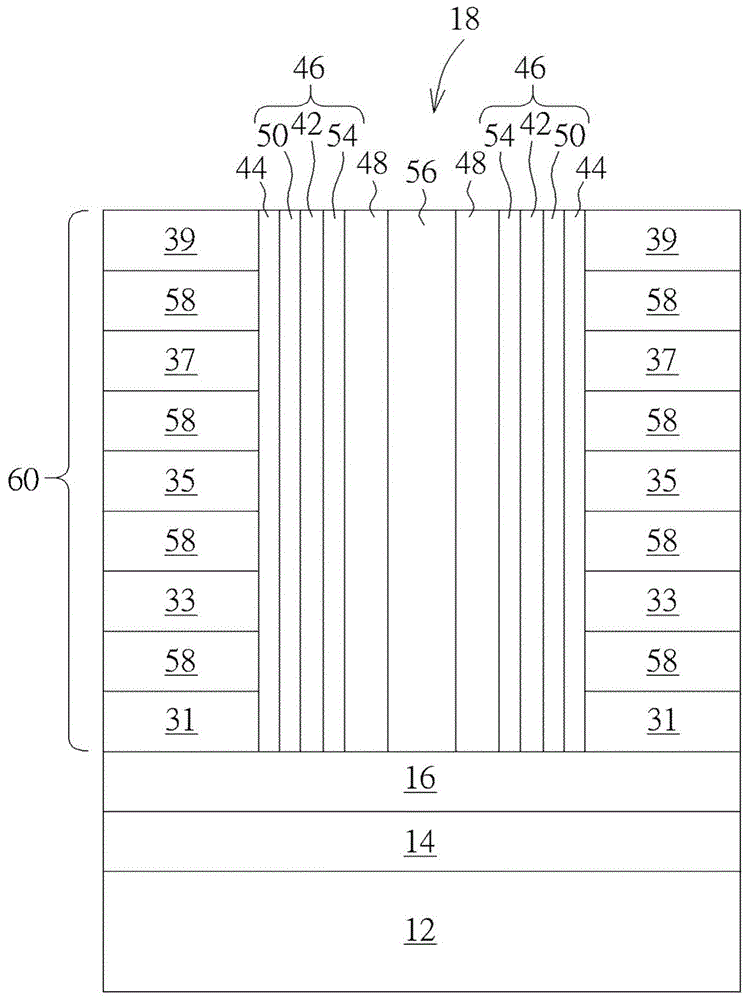
Description of the main elements
12 base
14 source line
16 lower select gate
18: channel structure
20 control gate structure
22: upper select gate
24 bit line
26 metal interconnect
28 contact plug
30 dielectric alternate stack structure
31 dielectric layer
32 dielectric layer
33 dielectric layer
34 dielectric layer
35 dielectric layer
36 dielectric layer
37 dielectric layer
38 dielectric layer
39 dielectric layer
42 passage opening
44 negative capacitance insulating layer
46 charge storage structure
48 channel layer
50 barrier layer
52 charge storage layer
54 tunneling layer
56 insulating layer
58 control gate layer
60 control gate structure
Detailed Description
Referring to fig. 1 to 5, fig. 1 is a schematic structural diagram of a 3D memory device according to an embodiment of the invention, and fig. 2 to 5 are schematic structural diagrams of a method for fabricating the channel structure in fig. 1 according to an embodiment of the invention. As shown in fig. 1 to 5, the 3D memory device mainly includes a channel structure 18 extending on a substrate 12 along a first direction, such as Y direction, a control gate structure 20 extending along a second direction, such as X direction, surrounding the channel structure 18, a source line 14 and a lower select gate 16 disposed below the control gate structure 20, an upper select gate 22, a bit line 24 and an upper metal interconnect 26 disposed above the control gate structure 20, and a plurality of contact plugs 28 connecting the source line 14, the lower select gate 16 and the upper metal interconnect 26.
In this embodiment, the step of forming the substrate 12 may include forming a bottom substrate, forming at least one peripheral circuit on the substrate, forming at least one interconnect structure electrically connected to the at least one peripheral circuit, and forming an epitaxial substrate on the at least one peripheral circuit. The underlying substrate may comprise any semiconductor material, such as silicon (e.g., single crystal silicon or polycrystalline silicon), silicon germanium (SiGe), gallium arsenide (GaAs), germanium (Ge), Silicon On Insulator (SOI) substrates, Germanium On Insulator (GOI) substrates, or combinations thereof. In some embodiments, the method of forming the underlying substrate may comprise a thinning process, which in turn may detail a grinding (grinding), dry/wet etching process, Chemical Mechanical Polishing (CMP), or a combination thereof.
The one or more peripheral circuits may include any digital, analog, and/or mixed signal peripheral circuits such as, but not limited to, page buffers, decoders, and latches, etc. In some embodiments, one or more interconnect structures may include any suitable conductive structure such as, but not limited to, contacts, single/multi-layer contact holes, conductive layers, plugs, and the like.
The epitaxial substrate may be formed on the peripheral circuit using a deposition process, which may include, but is not limited to, Chemical Vapor Deposition (CVD), Physical Vapor Deposition (PVD), Atomic Layer Deposition (ALD), or combinations thereof, for example. The epitaxial substrate may be a single-layer substrate or a multi-layer substrate, and may include a single-layer substrate of monocrystalline silicon, a single-layer substrate of polycrystalline silicon, or a multi-layer substrate composed of polycrystalline silicon and metal.
Then, as shown in fig. 2, a dielectric alternating stack structure 30 is formed on the substrate 12. In some embodiments, a plurality of dielectric layers 31, 32, 33, 34, 35, 36, 37, 38, 39 may be formed on the substrate 12 to constitute the dielectric alternating stack structure 30. In some embodiments, the material of the odd-numbered dielectric layers 31, 33, 35, 37, 39 is preferably different from the material of the even-numbered dielectric layers 32, 34, 36, 38, and each of the dielectric layers 31, 32, 33, 34, 35, 36, 37, 38, 39 may comprise a dielectric material such as, but not limited to, silicon oxide, silicon nitride, silicon oxynitride, or a combination thereof. In the present embodiment, the odd-numbered dielectric layers 31, 33, 35, 37, 39 preferably comprise silicon oxide and the even-numbered dielectric layers 32, 34, 36, 38 comprise silicon nitride, but the sequence is not limited thereto. The dielectric alternating stack structure 30 may be formed by one or more thin film deposition processes, such as Chemical Vapor Deposition (CVD), Physical Vapor Deposition (PVD), Atomic Layer Deposition (ALD), or any combination thereof. In addition, although nine dielectric layers are exemplified in the dielectric alternating stacked structure 30 of the present embodiment, the number of the dielectric layers is not limited thereto and can be adjusted according to the product requirement.
A plurality of via structures 18 are then formed in the dielectric alternating stack 30, wherein each via structure 18 may extend in a vertical direction and through the dielectric alternating stack 30. As shown in fig. 3, in some embodiments, forming the channel structure 18 includes forming a channel opening 42 through the dielectric alternating stack 30 in a vertical direction using, for example, wet etching and/or dry etching.
Next, as shown in fig. 4, a negative capacitance insulation layer 44, a charge storage structure 46 and a channel layer 48 are sequentially formed in the channel opening 42. In the present embodiment, the negative capacitance insulating layer 44 preferably includes but is not limited to hafnium zirconium Oxide (HfZrO)2) Lead zirconate titanate (PbZrTiO)3PZT), Bismuth ferrite (Bismuth ferrite, BiFeO3) A polyvinylidene fluoride-trifluoroethylene copolymer (P (VDF-TrFE)), or a combination thereof. In one embodiment, the negative-capacitance insulating layer 44 may be formed by one or more thin film deposition processes such as, but not limited to, an atomic layer deposition process, an epitaxial growth process, or a spin coating (spin coating) process.
The charge storage structure 46 may comprise a dielectric material such as, but not limited to, silicon oxide, silicon nitride, silicon-oxide-nitride-oxide (ONO), or combinations thereof. In detail, the charge storage structure 46 of the present embodiment includes a blocking layer 50, a charge storage layer 52 and a tunneling layer 54, wherein the blocking layer 50 includes silicon oxide, the charge storage layer 52 includes silicon nitride, and the tunneling layer 54 includes silicon oxide, but is not limited thereto. Channel layer 48 may comprise a semiconductor material such as, but not limited to, silicon, germanium, or a combination thereof.
Then, as shown in fig. 5, an insulating layer 56 may be formed to fill the channel opening 42, such that the insulating layer 56, the channel layer 48, the charge storage structure 46 and the negative capacitance insulating layer 44 form the channel structure 18. The even-numbered layers of the dielectric alternating stack structure 30, such as the dielectric layers 32, 34, 36, 38 comprising silicon nitride, are removed by etching, and one or more deposition processes are performed to form a conductive layer at the locations of the original even-numbered layers of the dielectric layers 32, 34, 36, 38 to form the control gate layer 58, wherein the control gate layer 58 and the single-numbered layers of the dielectric layers 31, 33, 35, 37, 39 together form a control gate structure 60. In the present embodiment, the insulating layer 56 may include, but is not limited to, silicon oxide, and the control gate layer 58 may include a conductive material such as, but not limited to, tungsten (W), cobalt (Co), copper (Cu), aluminum (Al), polysilicon, doped silicon, silicide, or any combination thereof.
It should be noted that although the present embodiment forms an additional insulating layer 56 to fill the via opening 42 after the formation of the via layer 48, the present invention is not limited thereto, and as shown in fig. 6, other embodiments according to the present invention can directly fill the via opening 42 during the formation of the via layer 48, so that the additional step of forming the insulating layer 56 after the formation of the via layer 48 can be omitted, and this variation also falls within the scope of the present invention. In addition, although the channel layer 48, the charge storage structure 46, and the negative capacitance insulating layer 44 are respectively disposed on both sides of the insulating layer 56 in a cross-sectional view, the channel layer 48, the charge storage structure 46, and the negative capacitance insulating layer 44 are actually disposed around the insulating layer 56 disposed at the center from the inside to the outside in a perspective view.
Subsequent fabrication processes for subsequent devices such as the top select gate 22, the bit line 24, the metal interconnect 26 and the contact plug 28 may be performed after the completion of the via structure 18 according to the fabrication process requirements. In the present embodiment, the select gate 22, the bit line 24, the metal interconnect 26, and the contact plug 28 may comprise a conductive material such as, but not limited to, tungsten (W), cobalt (Co), copper (Cu), aluminum (Al), polysilicon, doped silicon, silicide, or any combination thereof.
In summary, the present invention preferably forms a negative capacitance insulating layer between the control gate structure and the channel layer in the three-dimensional NAND (3D) memory device, and achieves the voltage amplification (voltage amplification) and power reduction (power reduction) effects through the negative capacitance insulating layer, thereby improving the device performance.
The above description is only a preferred embodiment of the present invention, and all equivalent changes and modifications made in the claims of the present invention should be covered by the present invention.
Claims (9)
Priority Applications (2)
| Application Number | Priority Date | Filing Date | Title |
|---|---|---|---|
| CN202010940210.4A CN114242729A (en) | 2020-09-09 | 2020-09-09 | Three-dimensional memory element |
| US17/065,508 US11832446B2 (en) | 2020-09-09 | 2020-10-07 | Three-dimensional memory device |
Applications Claiming Priority (1)
| Application Number | Priority Date | Filing Date | Title |
|---|---|---|---|
| CN202010940210.4A CN114242729A (en) | 2020-09-09 | 2020-09-09 | Three-dimensional memory element |
Publications (1)
| Publication Number | Publication Date |
|---|---|
| CN114242729A true CN114242729A (en) | 2022-03-25 |
Family
ID=80470060
Family Applications (1)
| Application Number | Title | Priority Date | Filing Date |
|---|---|---|---|
| CN202010940210.4A Pending CN114242729A (en) | 2020-09-09 | 2020-09-09 | Three-dimensional memory element |
Country Status (2)
| Country | Link |
|---|---|
| US (1) | US11832446B2 (en) |
| CN (1) | CN114242729A (en) |
Citations (3)
| Publication number | Priority date | Publication date | Assignee | Title |
|---|---|---|---|---|
| CN109994477A (en) * | 2017-12-27 | 2019-07-09 | 美光科技公司 | Memory cell and the method for forming memory cell |
| US20190304987A1 (en) * | 2018-03-28 | 2019-10-03 | Sandisk Technologies Llc | Ferroelectric non-volatile memory |
| CN110676260A (en) * | 2019-12-03 | 2020-01-10 | 长江存储科技有限责任公司 | Three-dimensional memory and forming method thereof |
Family Cites Families (15)
| Publication number | Priority date | Publication date | Assignee | Title |
|---|---|---|---|---|
| JP5416936B2 (en) * | 2008-09-02 | 2014-02-12 | 株式会社東芝 | Semiconductor device and manufacturing method thereof |
| KR101543331B1 (en) * | 2009-07-06 | 2015-08-10 | 삼성전자주식회사 | Method of fabricating vertical structure Non-volatile memory device having metal source line |
| US9484357B2 (en) * | 2014-12-16 | 2016-11-01 | Sandisk Technologies Llc | Selective blocking dielectric formation in a three-dimensional memory structure |
| US9716101B2 (en) * | 2015-05-20 | 2017-07-25 | Sandisk Technologies Llc | Forming 3D memory cells after word line replacement |
| JP2017168708A (en) * | 2016-03-17 | 2017-09-21 | 東芝メモリ株式会社 | Semiconductor memory device |
| JP6545649B2 (en) * | 2016-09-16 | 2019-07-17 | 東芝メモリ株式会社 | Memory device |
| KR102552461B1 (en) * | 2016-11-01 | 2023-07-06 | 삼성전자 주식회사 | Semiconductor devices and method of manufacturing the same |
| TWI605575B (en) * | 2017-01-20 | 2017-11-11 | 群聯電子股份有限公司 | Three-dimensional non-volatile memory structure and manufacturing method thereof |
| US11152386B2 (en) * | 2017-02-04 | 2021-10-19 | Monolithic 3D Inc. | 3D semiconductor device and structure |
| US10164009B1 (en) * | 2017-08-11 | 2018-12-25 | Micron Technology, Inc. | Memory device including voids between control gates |
| US10680006B2 (en) * | 2017-08-11 | 2020-06-09 | Micron Technology, Inc. | Charge trap structure with barrier to blocking region |
| US10734084B2 (en) * | 2018-05-31 | 2020-08-04 | Western Digital Technologies, Inc. | Scheme to reduce read disturb for high read intensive blocks in non-volatile memory |
| US10777576B1 (en) * | 2019-04-03 | 2020-09-15 | Micron Technology, Inc. | Integrated assemblies having charge-trapping material arranged in vertically-spaced segments, and methods of forming integrated assemblies |
| US10892016B1 (en) * | 2019-04-08 | 2021-01-12 | Monolithic 3D Inc. | 3D memory semiconductor devices and structures |
| US11729986B2 (en) * | 2020-05-28 | 2023-08-15 | Taiwan Semiconductor Manufacturing Company, Ltd. | Ferroelectric memory device and method of forming the same |
-
2020
- 2020-09-09 CN CN202010940210.4A patent/CN114242729A/en active Pending
- 2020-10-07 US US17/065,508 patent/US11832446B2/en active Active
Patent Citations (3)
| Publication number | Priority date | Publication date | Assignee | Title |
|---|---|---|---|---|
| CN109994477A (en) * | 2017-12-27 | 2019-07-09 | 美光科技公司 | Memory cell and the method for forming memory cell |
| US20190304987A1 (en) * | 2018-03-28 | 2019-10-03 | Sandisk Technologies Llc | Ferroelectric non-volatile memory |
| CN110676260A (en) * | 2019-12-03 | 2020-01-10 | 长江存储科技有限责任公司 | Three-dimensional memory and forming method thereof |
Also Published As
| Publication number | Publication date |
|---|---|
| US11832446B2 (en) | 2023-11-28 |
| US20220077179A1 (en) | 2022-03-10 |
Similar Documents
| Publication | Publication Date | Title |
|---|---|---|
| CN109417075B (en) | Multi-layer stacked three-dimensional memory device | |
| US11195857B2 (en) | Bonded three-dimensional memory devices and methods of making the same by replacing carrier substrate with source layer | |
| CN110121775B (en) | Interconnect structure for three-dimensional memory devices | |
| CN109417077B (en) | Memory Devices Using Comb Routing to Reduce Wire Loading | |
| CN110114880B (en) | Memory stack with silicon nitride gate to gate dielectric layer and method of forming the same | |
| JP7352660B2 (en) | semiconductor device | |
| TW202139437A (en) | 3d memory device with back source contact | |
| CN110088906B (en) | High-k dielectric layer in three-dimensional memory device and method of forming the same | |
| TW202013685A (en) | Semiconductor plug protected by protective dielectric layer in three-dimensional memory device and forming method thereof | |
| CN111937148A (en) | Three-dimensional memory device | |
| WO2020198943A1 (en) | Memory stacks having silicon oxynitride gate-to-gate dielectric layers and methods for forming the same | |
| TW202011579A (en) | Memory device using comb-like routing structure for reduced metal line loading | |
| TW202008568A (en) | Three-dimensional memory device | |
| TWI742886B (en) | Three-dimensional memory device with stable structure between storage blocks and method for forming the same | |
| CN108565266A (en) | Form the method and three-dimensional storage of three-dimensional storage | |
| TWI758123B (en) | Ferroelectric memory device and method of forming the same | |
| CN107393918A (en) | Semiconductor devices and the method for forming semiconductor devices | |
| CN113380821B (en) | Memory cell, memory device and method for forming the same | |
| TWI757019B (en) | Three dimensional memory device having supporting structure and manufacturing method thereof | |
| US20250331189A1 (en) | Three-dimensional memory devices and methods of manufacturing thereof | |
| CN114242729A (en) | Three-dimensional memory element | |
| US12089406B2 (en) | Three-dimensional memory device comprising contact pads exposed by an opening passing through layer stack and fabrication method thereof | |
| US20250176209A1 (en) | Semiconductor memory device and method of manufacturing the same | |
| CN116017984B (en) | Three-dimensional memory and its fabrication method | |
| TWI734594B (en) | Three-dimensional memory device |
Legal Events
| Date | Code | Title | Description |
|---|---|---|---|
| PB01 | Publication | ||
| PB01 | Publication | ||
| SE01 | Entry into force of request for substantive examination | ||
| SE01 | Entry into force of request for substantive examination |