Array substrate, display panel and display device thereof
Technical Field
The embodiment of the disclosure relates to the technical field of display, and in particular relates to an array substrate, a display panel of the array substrate and a display device of the array substrate.
Background
An Organic Light-Emitting Diode (OLED) display panel has the advantages of self-luminescence, high efficiency, bright color, Light weight, low power consumption, capability of being curled, wide temperature range of use and the like, and has been gradually applied to the fields of large-area display, illumination, vehicle-mounted display and the like.
Disclosure of Invention
The embodiment of the disclosure provides an array substrate, a related display panel and a related display device.
According to a first aspect of the present disclosure, there is provided an array substrate including a substrate. The array substrate further comprises a pixel array arranged on the substrate and comprising a plurality of sub-pixels arranged in a plurality of rows and a plurality of columns. Each sub-pixel has a pixel circuit and a data signal input, a scan signal input, a drive reset control signal input coupled to the pixel circuit. The pixel circuit includes a data writing circuit, a driving circuit, and a driving reset circuit. The driving circuit includes a control terminal, a first terminal, and a second terminal. The data writing circuit is coupled to the data signal input terminal, the scan signal input terminal, and the first terminal of the driving circuit, and is configured to provide the data signal to the first terminal of the driving circuit under the control of the scan signal. The driving circuit is configured to supply a driving current to the light emitting device. The driving reset circuit is coupled to the driving reset control signal input terminal, the control terminal of the driving circuit and the reset voltage source, and is configured to reset the control terminal of the driving circuit under the control of the driving reset control signal. The array substrate further comprises a plurality of pairs of scanning signal lines. The plurality of pairs of scanning signal lines extend in a row direction and are spaced apart from each other in a column direction. Each of the plurality of pairs of scanning signal lines includes a first scanning signal line and a second scanning signal line. The m-th pair of scanning signal lines corresponds to the m-th row of sub-pixels, and m is an integer of 1 or more. The first scanning signal line of the m-th pair of scanning signal lines is configured to supply a first scanning signal to the scanning input terminal of the sub-pixel of the 2n-1 th column of the m-th row of sub-pixels, n is an integer greater than or equal to 1, and the second scanning signal line of the m-th pair of scanning signal lines is configured to supply a second scanning signal to the scanning input terminal of the sub-pixel of the 2 n-th column of the m-th row. The array substrate further comprises a plurality of pairs of driving reset control signal lines. The plurality of pairs of driving reset control signal lines extend in a row direction and are spaced apart from each other in a column direction. Each of the plurality of pairs of driving reset control signal lines includes a first driving reset control signal line and a second driving reset control signal line. The m-th pair of driving reset control signal lines corresponds to the m-th row of sub-pixels. A first drive reset control signal line of the mth pair of drive reset control signal lines is configured to supply a first drive reset control signal to the drive reset control signal input terminal of the 2n-1 th column sub-pixel of the mth row sub-pixel, and a second drive reset control signal line of the mth pair of drive reset control signal lines is configured to supply a second drive reset control signal to the drive reset control signal input terminal of the 2n th column sub-pixel of the mth row sub-pixel. The first scanning signal line of the mth pair of scanning signal lines and the second driving reset control signal line of the mth pair of driving reset control signal lines are the same signal line.
In an embodiment of the present disclosure, the data writing circuit may include a data writing transistor. The driving reset circuit may include a driving reset transistor. The first pole of the data writing transistor may be coupled to a data input terminal, the second pole of the data writing transistor may be coupled to a first terminal of a driving circuit, and the control pole of the data writing transistor may be coupled to a scan signal terminal. The first pole of the driving reset transistor may be coupled to a control terminal of the driving circuit, the second pole of the driving reset transistor may be coupled to a reset voltage terminal, and the gate of the driving reset transistor may be coupled to a driving reset control signal input terminal. The first scanning signal line of the m-th pair of scanning signal lines may include a gate of the data writing transistor of the 2n-1 th column sub-pixel of the m-th row sub-pixel and a gate of the driving reset transistor of the 2 n-th column sub-pixel of the m-th row sub-pixel.
In an embodiment of the present disclosure, the pixel circuit may further include a compensation circuit, which may be coupled to the second terminal of the driving circuit, the control terminal of the driving circuit, and the scan signal input terminal, and configured to perform threshold compensation on the driving circuit according to the scan signal.
In an embodiment of the present disclosure, the compensation circuit may include a compensation transistor. The first pole of the compensation transistor may be coupled to the second terminal of the driving circuit, the second pole of the compensation transistor may be coupled to the control terminal of the driving circuit, and the gate of the compensation transistor may be coupled to the scan signal input terminal. The first scanning signal line of the m-th pair of scanning signal lines may further include a gate of the compensation transistor of the 2n-1 th column sub-pixel of the m-th row sub-pixel.
In an embodiment of the present disclosure, the pixel circuit may further include a storage circuit. The storage circuit may be coupled to the first voltage source and the control terminal of the driving circuit, and configured to store a voltage difference between the first voltage source and the control terminal of the driving circuit.
In an embodiment of the present disclosure, the sub-pixel may further include a light emission control signal terminal. The pixel circuit may further include a light emission control circuit. The light emitting control circuit may be coupled to the light emitting control signal terminal, the first voltage terminal, the driving circuit, and the light emitting device, and configured to apply the first voltage from the first voltage source to the driving circuit and apply the driving current generated by the driving circuit to the light emitting device.
In an embodiment of the present disclosure, the array substrate may further include a plurality of light emission control signal lines. The plurality of light emission control signals extend in a column direction and are spaced apart from each other in a row direction. The m-th light-emitting control signal line is configured to be coupled with the light-emitting control signal terminal of the m-th row of sub-pixels to provide a light-emitting control signal.
In an embodiment of the present disclosure, the sub-pixel may further include a light emission reset control signal input terminal. The pixel circuit further includes a light emission reset circuit. The light emission reset circuit is coupled to the light emission reset control signal input terminal, the reset voltage terminal, and the light emitting device, and configured to reset the light emitting device under the control of the light emission reset control signal.
In an embodiment of the present disclosure, the array substrate may further include a plurality of pairs of light emission reset control signal lines. The plurality of pairs of light emission reset control signal lines extend in a row direction and are arranged at intervals from each other in a column direction. Each of the plurality of pairs of light emission reset control signal lines includes a first light emission reset control signal line and a second light emission reset control signal line. The m-th pair of light-emitting reset control signal lines corresponds to the m-th row of sub-pixels. The first light emission reset control value signal line of the mth pair of light emission reset control signal lines is configured to supply the first light emission reset control signal to the light emission reset control signal input terminal of the 2n-1 th column sub-pixel of the mth row sub-pixel, and the second light emission reset control signal line of the mth pair of light emission reset control signal lines is configured to supply the second light emission reset control signal to the light emission reset control signal input terminal of the 2n th column sub-pixel of the mth row sub-pixel.
In an embodiment of the present disclosure, the first light emission reset control signal line of the m-th pair of light emission reset control signal lines and the first driving reset control signal line of the m + 1-th pair of driving reset control signal lines may be the same signal line. The second emission reset control signal line of the mth pair of emission reset control signal lines and the second driving reset control signal line of the (m + 1) th pair of driving reset control signal lines may be the same signal line.
In an embodiment of the present disclosure, the array substrate may further include a data signal line extending in a column direction. The data signal input end of each column of sub-pixels is connected to a corresponding data line to receive a data signal.
In an embodiment of the present disclosure, the array substrate may further include a reset power supply signal line extending in a column direction configured to supply a reset voltage to the corresponding pixel circuit.
In an embodiment of the present disclosure, the compensation circuit may include a compensation transistor. The light emission control circuit may include a first light emission control transistor and a second light emission control transistor. The light emission reset circuit may include a light emission reset transistor. The storage circuit may include a capacitor. The first pole of the driving transistor may be coupled to a first terminal of a driving circuit, the second pole of the driving transistor may be coupled to a second terminal of the driving circuit, and the gate of the driving transistor may be coupled to a control terminal of the driving circuit. A first pole of the data writing transistor may be coupled to the data signal input terminal, a second pole of the data writing transistor may be coupled to the first pole of the driving transistor, and a gate of the data writing transistor may be coupled to the scan signal input terminal. The first pole of the driving reset transistor may be coupled to the gate of the driving transistor, the second pole of the driving reset transistor may be coupled to the reset voltage terminal, and the gate of the driving reset transistor may be coupled to the driving reset control signal input terminal. The first pole of the compensation transistor may be coupled to the second pole of the driving transistor, the second pole of the compensation transistor may be coupled to the gate of the driving transistor, and the gate of the compensation transistor may be coupled to the scan signal input terminal. A first pole of the first light emission control transistor may be coupled to a first voltage terminal, a second pole of the first light emission control transistor may be coupled to a first pole of a driving transistor, and a gate of the first light emission control transistor may be coupled to a light emission control signal input terminal. The first pole of the second light emission control transistor may be coupled to the second pole of the driving transistor, the second pole of the second light emission control transistor may be coupled to the first pole of the light emitting device, and the gate of the second light emission control transistor may be coupled to the light emission control signal input terminal. A first pole of the light emitting reset transistor may be coupled to a first pole of the light emitting device, a second pole of the light emitting reset transistor may be coupled to a reset voltage terminal, and a gate of the light emitting reset transistor may be coupled to a light emitting reset control signal input terminal. A first pole of the capacitor may be coupled to the gate of the driving transistor and a second pole of the capacitor may be coupled to the first voltage terminal.
In an embodiment of the present disclosure, the array substrate may further include an active semiconductor layer on the substrate. The active semiconductor layer may include an active region of a transistor in the pixel circuit. For the mth row of subpixels: the active semiconductor layer of the 2n-1 th column of sub-pixels may include a first portion, a second portion, and a third portion disposed apart from each other. The first portion and the second portion are arranged in sequence in a row direction, and the combination of the first portion and the second portion and the third portion are arranged in sequence in a column direction. The first portion may include active regions driving reset transistors and compensation transistors in the 2n-1 th column of sub-pixels. The second portion may include an active region of the data writing transistor in the 2n-1 th column of sub-pixels. The third portion may include active regions of the driving transistor, the first light emission control transistor, the second light emission control transistor, and the light emission reset transistor in the 2n-1 th column of sub-pixels. The active semiconductor layer of the sub-pixel of the 2 n-th column includes a fourth portion and a fifth portion sequentially arranged in the column direction. The fourth portion may include active regions of the driving reset transistor, the data write transistor, the compensation transistor, the driving transistor, the first light emission control transistor, and the second light emission control transistor in the 2 nth column of sub-pixels. The fifth portion may include an active region of a light emitting reset transistor in a2 nth column of sub-pixels.
In an embodiment of the present disclosure, the array substrate may further include a first conductive layer located on a side of the active semiconductor layer away from the substrate. The first conductive layer may include a first driving reset control signal line, a first scanning signal line, a second scanning signal line, a first electrode of a capacitor, a light emission control signal line, a first light emission reset control signal line, and a second light emission reset control signal line, which are sequentially arranged in a column direction. The first scan signal line may serve as a second driving reset control signal line, and the first electrode of the capacitor may be integrated with the gate electrode of the driving transistor.
In an embodiment of the present disclosure, a portion of the first driving reset control signal line where an orthogonal projection on the substrate overlaps an orthogonal projection of the first portion of the active semiconductor layer on the substrate may be a gate of the driving reset transistor in the 2n-1 th column of sub-pixels. The portions of the first scan signal line where an orthogonal projection on the substrate overlaps with orthogonal projections of the first, second, and fourth portions of the active semiconductor layer on the substrate may be gates of the compensation transistor and the data write transistor in the 2n-1 th column of sub-pixels and the drive reset transistor in the 2 n-th column of sub-pixels, respectively. The portions of the second scanning signal line where the orthographic projection on the substrate overlaps the orthographic projection of the fourth portion of the active semiconductor layer on the substrate may be the gates of the data writing transistor and the compensation transistor in the 2 nth column of sub-pixels, respectively. The part of the orthographic projection of the first electrode of the capacitor in the sub-pixel of the 2n-1 th column on the substrate and the orthographic projection of the third part of the active semiconductor layer on the substrate can be the gate electrode of the driving transistor in the sub-pixel of the 2n-1 th column. The part of the orthographic projection of the first electrode of the capacitor in the sub-pixel of the 2 nth column on the substrate and the orthographic projection of the fourth part of the active semiconductor layer on the substrate can be the gate of the driving transistor in the sub-pixel of the 2 nth column. The portions of the light emission control signal line where an orthogonal projection on the substrate overlaps with orthogonal projections of the third portion and the fourth portion of the active semiconductor layer on the substrate may be gates of the first light emission control transistor and the second light emission control transistor in the 2n-1 th column of sub-pixels and the first light emission control transistor and the second light emission control transistor in the 2 n-th column of sub-pixels, respectively. The portion of the orthographic projection of the first light emission reset control signal line on the substrate overlapping the orthographic projection of the third portion of the active semiconductor layer on the substrate may be the gate of the light emission reset transistor in the 2n-1 th column of sub-pixels. A portion of the second light emission reset control signal line where an orthogonal projection on the substrate overlaps an orthogonal projection of the fifth portion of the active semiconductor layer on the substrate may be a gate of the light emission reset transistor in the 2 n-th column of sub-pixels.
In an embodiment of the present disclosure, the array substrate may further include a second conductive layer located on a side of the first conductive layer away from the substrate. The second conductive layer may include a second pole of the capacitor disposed in the column direction and a first power supply signal line as a first voltage source. The second pole of the capacitor and a projection of the first pole of the capacitor onto the substrate may at least partially overlap. The first power supply signal line extends in the row direction and may be integrally formed with the second pole of the capacitor.
In an embodiment of the present disclosure, the array substrate may further include a third conductive layer located on a side of the second conductive layer away from the substrate. The third conductive layer may include a data signal line, a reset power source signal line, a second power source signal line as a first voltage source, a third power source signal line as a first voltage source, a first connection portion, a second connection portion, a third connection portion, a fourth connection portion, a fifth connection portion, and a sixth connection portion. One end of the first connection portion may be coupled to a first pole of the compensation transistor of the 2n-1 th column sub-pixel, and the other end may be coupled to a second pole of the driving transistor of the 2n-1 th column sub-pixel. One end of the second connection portion may be coupled to the first electrode of the driving reset transistor of the sub-pixel in the 2n-1 th column, and the other end of the second connection portion may be coupled to the gate of the driving transistor of the sub-pixel in the 2n-1 th column. One end of the third connection portion may be coupled to the second pole of the data writing transistor of the sub-pixel of the 2n-1 th column, and the other end may be coupled to the first pole of the driving transistor of the sub-pixel of the 2n-1 th column. The fourth connection portion may be coupled to the second pole of the second emission control transistor of the sub-pixel of the 2n-1 th column. One end of the fifth connection portion may be coupled to the first electrode of the driving reset transistor of the sub-pixel in the 2n th column, and the other end of the fifth connection portion may be coupled to the gate of the driving transistor of the sub-pixel in the 2n th column. One end of the sixth connection portion may be coupled to the second pole of the second light-emitting control transistor of the sub-pixel in the 2n th column, and the other end of the sixth connection portion may be coupled to the first pole of the light-emitting reset transistor of the sub-pixel in the 2n th column. The data signal line may be coupled to a first pole of the data writing transistor of the 2n-1 th column sub-pixel and a first pole of the data writing transistor of the 2 n-th column sub-pixel. The second power signal line may extend in a column direction and be located in the 2n-1 column sub-pixel, and may couple the second pole of the capacitor of the 2n-1 column sub-pixel and the first pole of the first light emission control transistor. The third power signal line may extend in the column direction and be located in the 2 n-th column sub-pixel, and may couple the second pole of the capacitor of the 2 n-th column sub-pixel and the first pole of the first light emission control transistor.
In an embodiment of the present disclosure, the second conductive layer may further include a first additional reset power supply signal line and a second additional reset power supply signal line extending in the row direction. The first additional reset power supply signal line and the second additional reset power supply signal line may be coupled to a reset power supply signal line. The second pole of the capacitor and the first power supply signal line may be located between the first additional reset power supply signal line and the second additional reset power supply signal line in the column direction.
In an embodiment of the present disclosure, the array substrate may further include a third conductive layer located on a side of the second conductive layer away from the substrate. The third conductive layer may include a data signal line, a reset power signal line, a second power signal line as a first voltage source, a third power signal line as a first voltage source, a first connection portion, a second connection portion, a third connection portion, a fourth connection portion, a fifth connection portion, a sixth connection portion, a seventh connection portion, an eighth connection portion, a ninth connection portion, and a tenth connection portion. One end of the first connection portion may be coupled to a first pole of the compensation transistor of the 2n-1 th column sub-pixel, the other end of the first connection portion may be coupled to a second pole of the driving transistor of the 2n-1 th column sub-pixel, one end of the second connection portion may be coupled to a first pole of the driving reset transistor of the 2n-1 th column sub-pixel, and the other end of the second connection portion may be coupled to a gate of the driving transistor of the 2n-1 th column sub-pixel. One end of the third connection portion may be coupled to the second pole of the data writing transistor of the sub-pixel of the 2n-1 th column, and the other end may be coupled to the first pole of the driving transistor of the sub-pixel of the 2n-1 th column. The fourth connection portion may be coupled to the second pole of the second emission control transistor of the sub-pixel of the 2n-1 th column. One end of the fifth connection portion may be coupled to the first electrode of the driving reset transistor of the sub-pixel in the 2n th column, and the other end of the fifth connection portion may be coupled to the gate of the driving transistor of the sub-pixel in the 2n th column. One end of the sixth connection portion may be coupled to the second pole of the second light-emitting control transistor of the sub-pixel in the 2n th column, and the other end of the sixth connection portion may be coupled to the first pole of the light-emitting reset transistor of the sub-pixel in the 2n th column. One end of the seventh connecting portion may be coupled to the first additional reset power signal line, and the other end may be coupled to the second pole of the driving reset transistor of the 2n-1 th column of sub-pixels. One end of the eighth connecting portion may be coupled to the second additional reset power signal line, and the other end may be coupled to the second pole of the light emitting reset transistor of the sub-pixel of the 2n-1 th column. One end of the ninth connection portion may be coupled to the first additional reset power signal line, and the other end may be coupled to the second pole of the driving reset transistor of the sub-pixel of the 2 n-th column. One end of the tenth connection portion may be coupled to the second additional reset power signal line, and the other end may be coupled to the second pole of the light emitting reset transistor of the 2 n-th column of sub-pixels. The second power signal line may extend in a column direction and be located in the 2n-1 column sub-pixel, and may couple the second pole of the capacitor of the 2n-1 column sub-pixel and the first pole of the first light emission control transistor. The third power signal line may extend in the column direction and be located in the 2 n-th column sub-pixel, and may couple the second pole of the capacitor of the 2 n-th column sub-pixel and the first pole of the first light emission control transistor.
In an embodiment of the present disclosure, the array substrate may further include a fourth conductive layer located on a side of the third conductive layer away from the substrate. The fourth conductive layer may include a fourth power supply signal line as the first voltage source, an eleventh connection portion, and a twelfth connection portion. An orthogonal projection of the second power supply signal line on the substrate may at least partially overlap an orthogonal projection of the fourth power supply signal line on the substrate. An orthogonal projection of the third power supply signal line on the substrate may at least partially overlap an orthogonal projection of the fourth power supply signal line on the substrate. The fourth power signal line may be coupled to the second power signal line and the third power signal line. The eleventh connection portion may be coupled to the fourth connection portion. The twelfth connecting portion may be coupled to an end of the sixth connecting portion.
According to a second aspect of the present disclosure, a display panel is provided. The display panel includes the array substrate according to any one of the first aspect.
According to a third aspect of the present disclosure, a display device is provided. The display device includes the display panel according to any one of the second aspects.
Further aspects and ranges of adaptability will become apparent from the description provided herein. It should be understood that various aspects of the present application may be implemented alone or in combination with one or more other aspects. It should also be understood that the description and specific examples are intended for purposes of illustration only and are not intended to limit the scope of the present disclosure.
Drawings
The drawings described herein are for illustrative purposes only of selected embodiments and not all possible implementations, and are not intended to limit the scope of the present application, wherein:
fig. 1 shows a schematic structural diagram of an array substrate.
Fig. 2 shows a schematic structural diagram of an array substrate according to an embodiment of the present disclosure.
Fig. 3 shows a schematic block diagram of a sub-pixel according to an embodiment of the present disclosure.
Fig. 4 shows a schematic diagram of the pixel circuit in fig. 3, in accordance with an embodiment of the present disclosure.
Fig. 5 illustrates a timing diagram of signals driving the pixel circuit in fig. 4 according to an embodiment of the present disclosure.
Fig. 6 illustrates a timing diagram of signals driving the array substrate in fig. 2 according to an embodiment of the present disclosure.
Fig. 7-13 show schematic plan views of layers in an array substrate according to an embodiment of the present disclosure.
Fig. 14-15 show schematic plan layout views of stacked active semiconductor layers, first conductive layers, second conductive layers, third conductive layers, and fourth conductive layers.
Fig. 16 illustrates a schematic cross-sectional structure of the array substrate taken along the line A1a 1' in fig. 14 according to an embodiment of the present disclosure.
Fig. 17 illustrates a schematic cross-sectional structure of the array substrate taken along the line A2a 2' in fig. 15 according to an embodiment of the present disclosure.
Fig. 18 illustrates a schematic cross-sectional structure of the array substrate taken along the line B1B 1' in fig. 14 according to an embodiment of the present disclosure.
Fig. 19 illustrates a schematic cross-sectional structure of the array substrate taken along the line C1C 1' in fig. 14 according to an embodiment of the present disclosure.
Fig. 20 illustrates a schematic cross-sectional structure of the array substrate taken along the line C2C 2' in fig. 15, according to an embodiment of the present disclosure.
Fig. 21 illustrates a structural schematic diagram of a display panel according to an embodiment of the present disclosure.
Fig. 22 illustrates a schematic structural diagram of a display device according to an embodiment of the present disclosure.
Corresponding reference numerals indicate corresponding parts or features throughout the several views of the drawings.
Detailed Description
First, it should be noted that, unless the context clearly dictates otherwise, as used herein and in the appended claims, the singular forms of words include the plural and vice versa. Thus, when reference is made to the singular, it is generally intended to include the plural of the corresponding term. Similarly, the terms "comprising" and "including" are to be construed as being inclusive rather than exclusive. Likewise, the terms "include" and "or" should be construed as inclusive unless otherwise indicated herein. Where the term "example" is used herein, particularly when it comes after a set of terms, it is merely exemplary and illustrative and should not be considered exclusive or comprehensive.
In addition, it should be further noted that when introducing elements of the present application and the embodiments thereof, the articles "a," "an," "the," and "said" are intended to mean that there are one or more of the elements; "plurality" means two or more unless otherwise specified; the terms "comprising," "including," "containing," and "having" are intended to be inclusive and mean that there may be additional elements other than the listed elements; the terms "first," "second," "third," and the like are used for descriptive purposes only and are not to be construed as indicating or implying a relative importance or order of formation.
In the drawings, the thickness of layers and regions are exaggerated for clarity. It will be understood that when a layer, region or component is referred to as being "on" another part, it can be directly on the other part or intervening components may also be present. In contrast, when an element is referred to as being "directly on" another element, it is not intended that the other element be directly on the element.
Exemplary embodiments will now be described more fully with reference to the accompanying drawings.
In a common array substrate, because a plurality of rows of pixel units in the same row of pixel units are connected to the same scanning signal line, the plurality of rows of pixel units in the same row of pixel units are driven by the scanning signal provided by the same scanning line to be simultaneously opened, and the opening time of the plurality of rows of pixel units in the same row of pixel units is consistent; in addition, because the multiple columns of pixel units in the same row of pixel units are connected to multiple different data lines, the multiple columns of pixel units in the same row of pixel units can sequentially write data signals provided by the multiple different data lines. In this case, the multiple rows of pixel cells in the same row of pixel cells may have different charging manners, such as first charging and then discharging and then charging and discharging, which in turn may cause uneven display brightness of the multiple rows of pixel cells in the same row of pixel cells, and affect display quality.
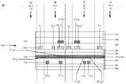
Fig. 1 shows a schematic structural view of an array substrate, which can solve the above-mentioned problems. As shown in fig. 1, the array substrate 10 includes a substrate, and a plurality of pairs of scanning signal lines S, a plurality of pairs of driving reset control signal lines R, and a pixel array disposed on the substrate. The pixel array includes a plurality of subpixels P arranged in a plurality of rows and a plurality of columns. As shown in fig. 1, the sub-pixel P has a pixel circuit and a Data signal input terminal Data, a scan signal input terminal Gate, and a driving reset control signal input terminal Rst1 coupled to the pixel circuit. In FIG. 1, P in the m-th row is shown2n-1Sub-pixel and P2nSub-pixel and P in sub-pixel of m +1 th row2n-1Sub-pixel and P2nA sub-pixel. In the embodiments of the present disclosure, m and n are each an integer of 1 or more.
As shown in fig. 1, the array substrate 10 includes two pairs of scan signal lines extending in a row direction and spaced apart from each other in a column direction, and a first scan signal line SO corresponding to the 2n-1 st and 2n +1 st columns of sub-pixels in the m-th rowmAnd a second scan signal line SE corresponding to the 2 n-th column sub-pixel and the 2n + 2-th column sub-pixel of the m-th rowmAnd a first scanning signal line SO corresponding to the sub-pixel of the 2n-1 column and the sub-pixel of the 2n +1 column of the m +1 th rowm+1And a second scan signal line SE corresponding to the sub-pixel of the 2n column and the sub-pixel of the 2n +2 column of the m +1 th rowm+1。
As shown in FIG. 1, the array substrate includes two pairs of driving reset control signal lines extending in a row direction and spaced apart from each other in a column direction, and a first driving reset control signal line RO corresponding to the 2n-1 column sub-pixel and the 2n +1 column sub-pixel of the m-th rowmAnd a second driving reset control signal line RE corresponding to the 2 n-th column sub-pixel and the 2n + 2-th column sub-pixel of the m-th rowmAnd a first driving reset control signal line RO corresponding to the sub-pixel of the 2n-1 column and the sub-pixel of the 2n +1 column of the m +1 th rowm+1And a second driving reset control signal line RE corresponding to the sub-pixel of the 2n column and the sub-pixel of the 2n +2 column of the m +1 th rowm+1。
In the array substrate shown in fig. 1, the scan signal input terminal of the sub-pixel of the 2n-1 th column in the sub-pixel of the m-th row may be connected to the first scan signal line SOmTo receive the first scan signal, the scan signal input terminal of the sub-pixel of the 2n th column in the sub-pixel of the m-th row can be connected to the second scan signal line SEmThe second scanning signal is received, so that the sub-pixels in the 2n-1 th column in the sub-pixels in the m-th row are driven to be turned on first by the first scanning signal, the sub-pixels in the 2 n-th column are driven to be turned on later by the second scanning signal, and the turn-on time of the sub-pixels in the 2n-1 th column in the sub-pixels in the m-th row is consistent with that of the sub-pixels in the 2n-1 th column. In this case, the m-th row sub-imageThe charging mode of the sub-pixels of the 2n-1 th column and the sub-pixels of the 2n th column in the pixel is the same, the problem of uneven display brightness of the sub-pixels of the multiple columns in the same row of pixel units is avoided, and the display quality can be improved.
However, with the array substrate shown in fig. 1, two scan signal generating circuits and two drive reset control signal generating circuits, which are generally disposed at the edge of the array substrate, need to be provided for each row of sub-pixels instead of one scan signal generating circuit and one drive reset control signal generating circuit as in the conventional case, which may disadvantageously increase the size of the bezel of the display panel.
In addition, as shown in fig. 1, the array substrate further includes a reset power signal line V and a data signal line D extending in the column direction and disposed apart from each other in the row direction. The 2n-1 th reset power supply signal line V2n-1… …, 2n +2 reset power supply signal lines V corresponding to the 2n-1 column of sub-pixels in each row of sub-pixels2n+2Corresponding to the 2n +2 th column of sub-pixels in each row of sub-pixels. Similarly, the 2n-1 th data signal line D2n-1 corresponds to the 2n-1 st column of sub-pixels in each row of sub-pixels, … …, and the 2n +2 th data signal line D2n +2 corresponds to the 2n +2 nd column of sub-pixels in each row of sub-pixels. In this case, since each sub-pixel has a separate reset power supply signal line and data line on the array substrate, which are not shared by other sub-pixels, the number of wirings on the array substrate is large, which results in a low PPI.
At least some embodiments of the present disclosure provide an array substrate, including: a plurality of pairs of scanning signal lines configured to extend in a row direction and arranged at intervals from each other in a column direction, each of the pairs of scanning signal lines including a first scanning signal line and a second scanning signal line; a plurality of pairs of driving reset control signal lines configured to extend in a row direction and arranged at intervals from each other in a column direction, each of the plurality of pairs of driving reset control signal lines including a first driving reset control signal line and a second driving reset control signal line; a plurality of data lines; and a pixel array including a plurality of sub-pixels arranged in a plurality of rows and a plurality of columns. Each of the plurality of sub-pixels includes a data signal input terminal, a scan signal input terminal, and a driving reset control signal input terminal. The multiple rows of sub-pixels correspond to the multiple pairs of scanning signal lines one by one, and each column of sub-pixels corresponds to one data line in the multiple data lines. The scanning signal input end of the sub-pixel of the 2n-1 th column (namely, an odd column) in the sub-pixel of the mth row is connected to the first scanning signal line in the mth pair of scanning signal lines to receive the first scanning signal, and m and n are integers which are more than or equal to 1; the scan signal input terminal of the 2 nth column (i.e., even column) subpixel in the mth row subpixel is connected to the second scan signal line of the mth pair of scan signal lines to receive the second scan signal. The driving reset control signal input end of the pixel unit of the 2n-1 column in the pixel unit of the mth row is connected to a first scanning signal line in the mth pair of scanning signal lines to receive a first scanning signal as a first driving reset control signal; and the driving reset control signal input end of the sub-pixel of the 2 nth column in the pixel unit of the mth row is connected to the second scanning signal line in the mth pair of scanning signal lines to receive a second scanning signal as a second driving reset control signal.
In the array substrate provided by the embodiment of the disclosure, the scan signal input terminal of the sub-pixel of the 2n-1 th column in the pixel unit of the m-th row may be connected to a first scan signal line of the m-th pair of scan signal lines to receive a first scan signal, the scan signal input terminal of the sub-pixel of the 2 n-th column in the sub-pixel of the m-th row may be connected to a second scan signal line of the m-th pair of scan signal lines to receive a second scan signal, so that the sub-pixels in the 2n-1 th column in the m-th row of pixel units are driven to be turned on first under the driving of the first scanning signal provided by the first scanning signal line in the m-th pair of scanning signal lines, the sub-pixels in the 2 n-th column are driven to be turned on later under the driving of the second scanning signal provided by the second scanning signal line in the m-th pair of scanning signal lines, and the opening time of the sub-pixel of the 2n-1 th column in the pixel unit of the m-th row and the sub-pixel of the 2 n-th column can be consistent. In this case, the charging mode of the sub-pixels of the 2n-1 th column and the sub-pixels of the 2n th column in the pixel unit of the m-th row is the same, so that the problem of uneven display brightness of the sub-pixels of the multiple columns in the sub-pixels of the same row is avoided, and the display quality can be improved.
In the array substrate provided by the embodiment of the present disclosure, the first scanning signal line of the mth pair of scanning signal lines and the second driving reset control signal line of the mth pair of driving reset control signal lines are the same signal line. Specifically, the scan signal input terminal of the 2n +1 th column sub-pixel in the m-th row sub-pixel may be connected to a first scan signal line of the m-th pair of scan signal lines, and the drive reset control signal input terminal of the 2 n-th column sub-pixel in the m-th row pixel unit may also be connected to a first scan signal line of the m-th pair of scan signal lines, so that a first scan signal, which is supplied to the 2n-1 th column sub-pixel in the m-th row sub-pixel by the m-th pair of scan signal lines, may be applied to the 2 n-th column sub-pixel in the m-th row sub-pixel as a first drive reset control signal to reset the 2 n-th column sub-pixel in the m-th row sub-pixel. In this case, the number of gate driver on array (GOA) devices integrated on the array substrate may be reduced, which is advantageous for implementing a narrow bezel design of a display device using the array substrate.
In an embodiment of the present disclosure, the sub-pixel may further include a reset voltage terminal. The array substrate further comprises a plurality of reset power supply signal lines. The plurality of reset power supply signal lines extend in a column direction and are alternately arranged with the data signal lines in a row direction, and intervals between the data signal lines adjacent to each other and between the reset power supply signal lines adjacent to each other each define a column of the sub-pixels. The reset power supply signal line is configured to supply a reset voltage to a reset voltage terminal of a sub-pixel in a sub-pixel column adjacent to the reset power supply signal line. Specifically, the (n + 1) th reset power supply signal line Vn +1 is adjacent to the 2 n-th column sub-pixel and the 2n + 1-th column sub-pixel, and is configured to supply a reset voltage to the reset voltage terminals of the 2 n-th column sub-pixel and the 2n + 1-th column sub-pixel. The data signal line is configured to supply a data signal to a data signal input terminal of a sub-pixel in a sub-pixel column adjacent to the data signal line. Specifically, the nth data signal line Dn is adjacent to the 2n-1 th and 2 n-th column sub-pixels and configured to supply a data signal to data signal input terminals of the 2n-1 th and 2 n-th column sub-pixels. The (n + 1) th data signal line Dn +1 is adjacent to the (2 n + 1) th column sub-pixel and the (2 n + 2) th column sub-pixel, and is configured to supply a data signal to the data signal input terminals of the (2 n + 1) th column sub-pixel and the (2 n + 2) th column sub-pixel. In this case, the number of arranged data lines integrated on the array substrate may be reduced, thereby improving the PPI.
In the following, the array substrate provided by the embodiments of the present disclosure is described in non-limiting manner with reference to the drawings, and as described below, different features of the embodiments can be combined with each other without conflicting with each other, so as to obtain new embodiments, and the new embodiments also belong to the scope of the present disclosure.
Fig. 2 is a schematic structural diagram of an array substrate according to some embodiments of the present disclosure.
As shown in fig. 2, the array substrate 20 includes a substrate, and a plurality of pairs of scanning signal lines S, a plurality of pairs of driving reset control signal lines R, a plurality of reset power supply signal lines V, a plurality of data lines D, and a pixel array disposed on the substrate. The substrate may be a glass substrate, a plastic substrate, or the like, and embodiments of the present disclosure are not limited thereto. A plurality of pairs of scan signal lines S may extend in a row direction and be disposed on the substrate at intervals from each other in a column direction, each of the plurality of pairs of scan signal lines S including a first scan signal line SO and a second scan signal line SE; a plurality of pairs of driving reset control signal lines R may extend in a row direction and be disposed on the substrate at intervals from each other in a column direction, and may include a first driving reset control signal line RO and a second driving reset control signal line RE; a plurality of reset power lines V and a plurality of data lines D are alternately disposed on the substrate along a row direction with each other, and an interval between the data signal lines and the reset power signal lines adjacent to each other defines a column of the sub-pixels; the pixel array includes a plurality of sub-pixels P arranged in a plurality of rows and columns, for example, in a pixel region defined by intersections of a plurality of pairs of scanning signal lines S and a plurality of reset power signal lines V and a plurality of data lines D, each of the sub-pixels P includes a scanning signal input terminal Gate, a data signal input terminal DA, a driving reset control signal input terminal Rst1 and a reset voltage terminal VINT to receive a scanning signal (e.g., a first scanning signal or a second scanning signal), a data signal, a driving reset control signal (e.g., a first driving reset control signal or a second driving reset control signal), a reset voltage, respectively, for the pixel unit P.
For example, the first direction may be perpendicular to the second direction, the first direction may be a row direction of the pixel array (e.g., X direction in fig. 2), and the second direction may be a column direction of the pixel array (e.g., Y direction in fig. 2).
As shown in fig. 2, a plurality of rows of pixel units may be in one-to-one correspondence with a plurality of pairs of scanning signal lines S, each row of pixel units may be connected to a pair of scanning signal lines S corresponding thereto, for example, an mth row of sub-pixels may correspond to an mth pair of scanning signal lines SmThe sub-pixel of the 2n-1 th column in the m-th row of sub-pixels may correspond to the m-th pair of scanning signal lines SmFirst scanning signal line SOmThe sub-pixel of the 2n th column in the m-th row pixel unit may correspond to S in the m-th pair of scanning signal linesmSecond scanning signal line SEmThe scan signal input terminal Gate of the 2n-1 th column sub-pixel in the m-th row pixel unit may be connected to the m-th pair of scan signal lines SmFirst scanning signal line SOmTo receive the first scan signal, the scan signal input terminal Gate of the 2 n-th column sub-pixel in the m-th row of pixel units may be connected to the second scan signal line SE in the m-th pair of scan signal lines SmmTo receive the second scanning signal, m and n are integers greater than or equal to 1.
As shown in fig. 2, a plurality of rows of pixel cells may correspond one-to-one to a plurality of pairs of driving reset control signal lines R. Each row of pixel cells may be connected to a corresponding pair of driving reset control signal lines R, e.g., the mth row of subpixels may correspond to the mth pair of driving reset control signal lines RmThe sub-pixel of the 2n-1 th column in the m-th row of sub-pixels may correspond to the m-th pair of driving reset control signal lines RmFirst driving reset control signal line RO in (1)mThe sub-pixels of the 2n th column in the m-th row of pixel units may correspond to the m-th pair of driving reset control signal lines RmSecond driving reset control signal line REmThe driving reset control signal input terminal Rst1 of the sub-pixel of the 2n-1 th column in the m-th row of pixel units may be connected to the first driving reset control signal RO of the m-th pair of driving reset control signals RmmTo receive the first driving reset control signal, the driving reset control signal input terminal Rst1 of the 2 nth column sub-pixel in the mth row pixel unit may be connected to the mth pair driving reset control signal RmSecond driving reset control signal RE in (1)mTo receive the second scan signal.
As shown in fig. 2, the m-th pair of scanning signal lines SmFirst scanning signal line SOmAnd the m-th pair of driving reset control signal lines RmSecond driving reset control signal line REmAre the same signal line. Specifically, the driving reset control signal input terminal Rst1 of the 2 nth column sub-pixel in the mth row sub-pixel may be connected to the mth pair of scanning signal lines SmFirst scanning signal line SOm/RE mTo receive a first scanning signal. In this case, the first scanning signal line SO of the m-th pair of scanning signal lines SmmThe first scan signal supplied to the 2 nth column of subpixels of the mth row of subpixels may be applied to the 2 nth column of subpixels of the mth row of subpixels as a first driving reset control signal to reset the 2 nth column of subpixels of the mth row of subpixels.
As shown in fig. 2, the data signal line D is configured to supply a data signal to a data signal input terminal of a sub-pixel in a sub-pixel column adjacent to the data signal line. Specifically, the 2n-1 column sub-pixel and the 2n column sub-pixel may correspond to the same data line Dn, the 2n +1 column sub-pixel and the 2n +2 column sub-pixel may correspond to the same data line Dn +1, … …, and so on. The Data signal input terminal Data of the sub-pixel of the 2n-1 th column and the Data signal input terminal Data of the sub-pixel of the 2n-2 n column may be connected to the same Data line Dn to receive a Data signal, and the Data signal input terminal Data of the sub-pixel of the 2n +1 th column and the Data signal input terminal Data of the sub-pixel of the 2n +2 nd column may be connected to the same Data line Dn+1To receive data signals, … …, and so on.
As shown in fig. 2, the reset power supply signal line V is configured to supply a reset voltage to a reset voltage terminal of a sub-pixel in a sub-pixel column adjacent to the reset power supply signal line. Specifically, the 2 n-th column sub-pixel and the 2n + 1-th column sub-pixel may correspond to the same reset power supply signal line Vn+1The 2n +2 th column sub-pixel and the 2n +3 th column sub-pixel (not shown) may correspond to the same reset power supply signal line Vn +2, … …, and so on. The reset voltage terminal Vint of the 2 n-th column sub-pixel and the reset voltage terminal Vint of the 2n + 1-th column sub-pixel may be connected to the same reset power supply signal line Vn+1To receive the reset voltage, the reset voltage terminal Vint of the 2n +2 th column sub-pixel and the reset voltage terminal Vint of the 2n +3 th column sub-pixel may be connected to the same reset power signal line Vn+2To receive a reset voltage, … …, and so on.
As shown in fig. 2, the nth reset power supply signal line Vn is disposed at the left side of the sub-pixels of the 2n-1 th column and the nth data line Dn is disposed at the right side of the sub-pixels of the 2n-1 th column, one column of sub-pixels is disposed between the nth reset power supply signal line Vn and the nth data line Dn, and two columns of sub-pixels may be disposed between the adjacent two data lines D. Two columns of sub-pixels may be disposed between two adjacent reset power supply signal lines V. It is apparent that embodiments of the present disclosure are not limited thereto. For example, the nth reset power supply signal line Vn is disposed at the right side of the 2n-1 th column sub-pixel, and the nth data line Dn may be disposed at the left side of the 2n-1 th column sub-pixel.
In some embodiments of the present disclosure, the subpixel P further includes a light emission reset control signal input Rst 2. The array substrate 20 further includes a plurality of pairs of light-emitting reset control signal lines (not shown). And a plurality of pairs of light-emitting reset signal lines extending in the row direction and arranged at intervals from each other in the column direction. Each of the plurality of pairs of light emission reset signal lines includes a first light emission reset control signal line and a second light emission reset control signal line. The m-th pair of light-emission reset signal lines corresponds to the m-th row sub-pixels, and a first light-emission reset signal line of the m-th pair of light-emission reset signal lines is configured to supply a first light-emission reset signal to light-emission reset signal input terminals of the 2n-1 th column sub-pixels of the m-th row sub-pixels. The second emission reset signal line of the m-th pair of emission reset signal lines is configured to supply the second emission reset signal to the emission reset signal input terminal of the 2 n-th column sub-pixel of the m-th row sub-pixel.
In this embodiment, the first light emission reset signal line of the mth pair of light emission reset signal lines and the first driving reset control signal line of the m +1 th pair of driving reset control signal lines are the same signal line. The second light-emitting reset signal line of the mth pair of light-emitting reset signal lines and the second driving reset control signal line of the (m + 1) th pair of driving reset control signal lines are the same signal line. Specifically, the light emission reset control signal input terminal of the sub-pixel of the 2n-1 th column in the sub-pixel of the m-th row is connected to the first scanning signal line of the m +1 th pair of scanning signal lines to receive the first scanning signal supplied from the first scanning signal line of the m +1 th pair of scanning signal lines as the first light emission reset control signal to reset the sub-pixel of the 2n-1 th column in the sub-pixel of the m-th row. In this case, the m +1 th pair of scanning signal lines Sm+1First scanning signal line SOm+1The first scan signal supplied to the 2n-1 th column sub-pixel of the m-th row sub-pixel may be applied to the 2n-1 th column sub-pixel of the m-th row sub-pixel as a light emission reset control signal to reset the 2n-1 th column sub-pixel of the m-th row sub-pixel. The light emitting reset control signal input end of the sub-pixel of the 2 nth column in the sub-pixel of the mth row is connected to the second scanning signal line in the m +1 th pair of scanning signal lines to receive the second scanning signal provided by the m +1 th pair of scanning signal lines as a second light emitting reset control signal to reset the sub-pixel of the 2 nth column in the sub-pixel of the mth row. In this case, the m +1 th pair of scanning signal lines Sm+1Second scanning signal line SE inm+1The second scan signal supplied to the 2 nth column sub-pixels in the mth row sub-pixels may be applied to the 2 nth column sub-pixels in the mth row sub-pixels as a light emission reset control signal to reset the 2 nth column sub-pixels in the mth row sub-pixels.
As shown in FIG. 2, the reset signal input terminal RST of the sub-pixel of the 2n-1 th column in the m-th row of sub-pixels may be connected to the m-1 th pair of scanning signal lines Sm-1First scanning signal line SOm-1. In this case, the first scanning signal line SO of the m-1 th pair of scanning signal lines Sm-1m-1The first scan signal supplied to the nth column of sub-pixels in the m-1 th row of sub-pixels may be applied to the nth column of sub-pixels in the mth row of sub-pixels as a second reset signal to reset the nth column of sub-pixels in the mth row of sub-pixels.
Further, as shown in FIG. 2, the light emission reset control signal input terminal Rst2 of the sub-pixel of the 2n-1 th column in the m-th row sub-pixel is connected to the m + 1-th pair of scanning signal lines Sm+1First scanning signal line SOm+1In the case of (3), the light emission reset control signal input terminal Rst2 of the 2 n-th column sub-pixel in the m-th row sub-pixel is connected to the m + 1-th pair of scanning signal lines Sm+1Second scanning signal line SE inm+1. In this case, the reset modes of the sub-pixels of the 2n-1 th column and the sub-pixels of the 2 n-th column in the sub-pixels of the m-th row are different from the reset modes of the sub-pixels of the 2n-1 th column and the sub-pixels of the 2 n-th column in the sub-pixels of the m +1 th row. Specifically, regarding the respective working periods of the m-th row sub-pixels and the m + 1-th row sub-pixels, in the m-th row sub-pixels, the 2 n-1-th column sub-pixels are reset by using the first scanning signal supplied to the 2 n-1-th column sub-pixels in the m + 1-th row sub-pixels as a light-emitting reset control signal; in the m row sub-pixels, the 2n column sub-pixels are reset by using the second scanning signal supplied to the 2n column sub-pixels in the m +1 row sub-pixels as the light emitting reset control signal.
In some embodiments of the present disclosure, the subpixel P further comprises a light emission control signal input to receive a light emission control signal for the subpixel. Accordingly, the array substrate 20 provided in this embodiment may further include a plurality of light emission control signal lines extending in the column direction and disposed on the substrate at intervals in the row direction, the plurality of light emission control signal lines corresponding to the plurality of rows of sub-pixels one-to-one, and the light emission control signal input terminal of the mth row of sub-pixels being connected to the mth light emission control signal line to receive the light emission control signal.
As shown in fig. 2, each sub-pixel P further includes an emission control signal input terminal EM. Array substrate 20A plurality of light emission control signal lines E disposed on the substrate may be further included, and for example, the plurality of light emission control signal lines E may be disposed on the substrate in the first direction. The plurality of light emission control signal lines E may correspond one-to-one to the plurality of rows of sub-pixels, and each row of sub-pixels may be connected to one light emission control signal line E corresponding thereto. For example, the m-th row of sub-pixels corresponds to the m-th emission control signal line EmThe emission control signal input terminals EM of the m-th row of sub-pixels may be connected to the m-th emission control signal line EmTo receive the light emission control signal.
It should be noted that, although the m-th light emission control signal line E is shown in fig. 2mIs disposed at an upper side of the mth row of sub-pixels, but embodiments of the present disclosure are obviously not limited thereto. For example, the m-th light emission control signal line EmMay be disposed at the lower side of the m-th row of sub-pixels.
In some embodiments of the present disclosure, the sub-pixel P may further include a first voltage terminal VDD. The array substrate may further include a plurality of first voltage signal lines disposed on the substrate. The plurality of first voltage signal lines correspond to the plurality of rows of sub-pixels one to one, a first voltage terminal of a 2n-1 column sub-pixel in the m-th row sub-pixel is connected to the 2n-1 first voltage signal line to receive a first voltage, … …, and a first voltage terminal of a 2n +2 column sub-pixel in the m-th row sub-pixel is connected to the 2n +2 first voltage signal line to receive the first voltage.
Fig. 3 is a schematic block diagram of a sub-pixel in accordance with some embodiments of the present disclosure. As shown in fig. 3, the sub-pixel P includes a pixel circuit 100 and a light emitting device 200. The pixel circuit 100 includes a data writing circuit 110, a driving circuit 120, a driving reset circuit 130, a compensation circuit 140, a light emission control circuit 150, a light emission reset circuit 160, and a storage circuit 170.
As shown in fig. 3, the data writing circuit 110 is coupled to the data signal input terminal, and the first terminal F of the driving circuit 120 is coupled to the scan signal input terminal Gate. The data writing circuit is configured to write a data signal into the driving circuit 120 under the control of the scan signal. For example, the scan signal may be the first scan signal or the second scan signal described in the previous embodiment, and the scan signals mentioned in the subsequent embodiments have similar meanings, and thus will not be described in detail.
As shown in fig. 3, the driving circuit 120 includes a control terminal G, a first terminal F, and a second terminal S, and is configured to provide a driving circuit to the light emitting device 200 under the control of a control signal from the control terminal G.
As shown in fig. 3, the driving reset circuit 130 is coupled to the control terminal G of the driving circuit 120, the reset voltage terminal Vint and the driving reset control signal input terminal Rst1, and is configured to apply a reset voltage received from the reset voltage terminal Vint to the driving circuit 120 under the control of the driving reset control signal to reset the control terminal G of the driving circuit 120. For example, the driving reset control signal may be the first driving reset control signal or the second driving reset control signal described in the previous embodiment, and the driving reset control signal mentioned in the subsequent embodiment has similar meaning, and thus will not be described again.
As shown in fig. 3, the compensation circuit 140 is coupled to the control terminal G of the driving circuit 120, the second terminal S of the driving circuit 120, and the scan signal input terminal Gate, and is configured to perform threshold compensation on the driving circuit under the control of the first scan signal or the second scan signal from the scan signal input terminal Gate.
As shown in fig. 3, the light emission control circuit 150 is coupled to the first terminal F of the driving circuit 120, the second terminal S of the driving circuit 120, and the light emission control signal input terminal EM, and is configured to apply a first voltage received from the first voltage terminal VDD to the driving circuit 120 under the control of the light emission control signal, thereby applying a driving current generated by the driving circuit 120 to the light emitting device 200.
As shown in fig. 3, the light emission reset circuit 160 is coupled to the light emitting device 200, a reset voltage terminal VINT, and a light emission reset control signal input terminal Rst2, and is configured to apply a reset voltage received from the reset voltage terminal VINT to the light emitting device 200 under the control of a light emission reset control signal to reset the light emitting device 200. For example, the light emission reset control signal may be the first light emission reset control signal or the second light emission reset control signal described in the previous embodiment, and the light emission reset control signal mentioned in the subsequent embodiment has similar meaning, and thus will not be described again.
As shown in fig. 3, the storage circuit 170 is coupled to the first voltage terminal VDD and the control terminal G of the driving circuit 120, and is configured to store a voltage difference between the first voltage from the first voltage terminal VDD and the voltage of the control terminal G of the driving circuit 120.
As shown in fig. 3, the light emitting device 200 is coupled to the second voltage source VSS and the second terminal S of the driving circuit 120, and is configured to emit light under the driving of the driving current generated by the driving circuit 120.
For example, the light emitting device 200 may be a light emitting diode or the like. The light emitting diode may be an Organic Light Emitting Diode (OLED), a quantum dot light emitting diode (QLED), or the like.
Fig. 4 is a schematic diagram of the pixel circuit in fig. 3. As shown in fig. 4, the data writing circuit 110 includes a data writing transistor T1, the driving circuit 120 includes a driving transistor T2, the driving reset circuit 130 includes a driving reset transistor T3, the compensation circuit 140 includes a compensation transistor T4, the light emission control circuit 150 includes a first light emission control transistor T5 and a second light emission control transistor T6, the light emission reset circuit 160 includes a light emission reset transistor T7, and the storage circuit 170 includes a capacitor C.
As shown in fig. 4, a first pole of the driving transistor T2 is coupled to the first terminal F of the driving circuit 120, a second pole of the driving transistor T2 is coupled to the second terminal S of the driving circuit 120, and a gate of the driving transistor T2 is coupled to the control terminal G of the driving circuit 120.
As shown in fig. 4, a first pole of the Data writing transistor T1 is coupled to the Data signal input terminal Data to receive a Data signal from the Data signal line D; the second pole of the data write transistor T1 is coupled to the first pole of the driving transistor T2; the Gate of the data write transistor T1 is coupled to the scan signal input terminal Gate to receive the first scan signal or the second scan signal from the scan signal input terminal Gate, and is configured to supply the data signal from the data signal line D to the first pole of the driving transistor T2 according to the first scan signal or the second scan signal from the scan signal input terminal Gate.
As shown in fig. 4, the first pole of the driving reset transistor T3 is coupled to the gate of the driving transistor T2; the second pole of the driving reset transistor T3 is coupled to the reset voltage terminal VINT to receive the reset voltage from the reset voltage terminal VINT; the gate of the driving reset transistor T3 is coupled to the driving reset control signal input terminal Rst1 to receive the first driving reset control signal or the second driving reset control signal from the driving reset control signal input terminal Rst1, and is configured to supply a reset voltage to the gate of the driving transistor T2 to reset the gate of the driving transistor T2 according to the first driving reset control signal or the second driving reset control signal from the driving reset control signal input terminal Rst 1.
As shown in fig. 4, a first pole of the compensation transistor T4 is coupled to a second pole of the driving transistor T2; the second pole of the compensation transistor T4 is coupled to the gate of the driving transistor T2; the Gate of the compensation transistor T4 is coupled to the scan signal input terminal Gate to receive the first scan signal or the second scan signal from the scan signal input terminal Gate, and is configured to compensate the threshold of the driving transistor T2 according to the first scan signal or the second scan signal from the scan signal input terminal Gate.
As shown in fig. 4, a first pole of the first light emitting control transistor T5 is coupled to the first voltage terminal VDD to receive a first voltage from the first voltage terminal VDD; a second pole of the first light emitting control transistor T5 is coupled to the first pole of the driving transistor T2; the gate of the first light emitting control transistor T5 is coupled to the light emitting control signal input terminal EM to receive the light emitting control signal from the light emitting control signal input terminal EM, and is configured to control on/off between the first voltage terminal VDD and the first pole of the driving transistor T2 according to the light emitting control signal from the light emitting control signal input terminal EM, thereby controlling whether the first voltage from the first voltage terminal VDD is supplied to the first pole of the driving transistor T2.
A first pole of the second light emission controlling transistor T6 is coupled to a second pole of the driving transistor T2; a second pole of the second light emission controlling transistor T6 is coupled to the first pole of the light emitting device 200; the gate of the second emission control transistor T6 is coupled to the emission control signal input terminal EM to receive an emission control signal from the emission control signal input terminal EM, and is configured to control on/off between the second pole of the driving transistor T2 and the first pole of the light emitting device 200 according to the emission control signal from the emission control signal input terminal EM, thereby controlling whether the current generated by the driving transistor is supplied to the light emitting device 200.
Under the control of the light emission control signal, the first and second light emission control transistors T5 and T6 are collectively configured to apply a first voltage to the driving circuit 120 and apply a driving current generated by the driving circuit 120 to the light emitting device 200.
As shown in fig. 4, a first pole of the capacitor C is coupled to the gate of the driving transistor T2; the second pole of the capacitor is coupled to the first voltage terminal VDD and is configured to store a voltage difference between the first voltage from the first voltage terminal VDD and the voltage of the gate of the driving transistor T2.
It should be noted that the embodiments of the present disclosure are described by taking as examples that the reset voltage terminal VINT inputs a low voltage, the first voltage terminal VDD inputs a high voltage, the second voltage terminal VSS inputs a low voltage, or the second terminal of the light emitting device 120 is grounded, and here, high and low only indicate a relative magnitude relationship between the input voltages.
Note that, all the transistors used in the embodiments of the present disclosure may be thin film transistors, field effect transistors, or other switching devices with the same characteristics, and the thin film transistors are used as examples in all the embodiments of the present disclosure. The source and drain of the transistor used herein may be symmetrical in structure, so that there may be no difference in structure between the source and drain. In the embodiments of the present disclosure, in order to distinguish two poles of a transistor except for a gate, one of them is directly described as a first pole, and the other is a second pole.
In addition, it should be noted that the transistors used in the embodiments of the present disclosure may be P-type transistors or N-type transistors, and it is only necessary to connect the respective poles of the selected type of transistors with reference to the respective poles of the corresponding transistors in the embodiments of the present disclosure, and to enable the corresponding voltage terminals to provide the corresponding high voltage or low voltage. For example, for an N-type transistor, the input terminal is a drain, the output terminal is a source, and the control terminal is a gate; for a P-type transistor, its input terminal is the source and its output terminal is the drain, and its control terminal is the gate. The level of the control signal at the control terminal of the transistors is also different for different types of transistors. For example, for an N-type transistor, when the control signal is high, the N-type transistor is in a conducting state; and when the control signal is in a low level, the N-type transistor is in a cut-off state. For a P-type transistor, when the control signal is at a low level, the P-type transistor is in a conducting state; and when the control signal is high level, the P-type transistor is in a cut-off state. When an N-type transistor is used, an Oxide semiconductor, such as Indium Gallium Zinc Oxide (IGZO), may be used as an active layer of the thin film transistor, and compared to using Low Temperature Polysilicon (LTPS) or amorphous Silicon (e.g., hydrogenated amorphous Silicon) as an active layer of the thin film transistor, the size of the transistor may be effectively reduced and leakage current may be prevented. Low temperature polysilicon generally refers to the case where the crystallization temperature of polysilicon obtained by crystallization of amorphous silicon is below 600 degrees celsius.
It should be noted that, in the embodiment of the present disclosure, the pixel circuit of the sub-pixel may be a structure including other numbers of transistors, such as a 7T2C structure, a 6T1C structure, a 6T2C structure, or a 9T2C structure, in addition to the 7T1C (i.e., seven transistors and one capacitor) structure shown in fig. 4, which is not limited in the embodiment of the present disclosure.
Fig. 5 is a timing diagram of signals driving the pixel circuit in fig. 4. As shown in fig. 5, the operation process of the pixel circuit 100 includes three phases, i.e., a reset phase P1, a data writing and compensation phase P2, and a light emitting phase P3.
The operation of the pixel circuit in fig. 5 will be described with reference to fig. 4, taking as an example that the data writing transistor T1, the driving transistor T2, the driving reset transistor T3, the compensating transistor T4, the first light emission control transistor T5, the second light emission control transistor T6, and the light emission reset transistor are all P-type transistors.
As shown in fig. 5, in the reset phase P1, a driving reset control signal RST of a low level, a scan signal GA of a high level, a light emission control signal EMS of a high level, and a data signal DA of a low level are input.
In the reset phase P1, the gate of the driving reset transistor T3 receives the driving reset control signal RST1 of low level, and the driving reset transistor T3 is turned on, so that the reset voltage VINT is applied to the gate of the driving transistor T2 to reset the gate of the driving transistor T2, so that the driving transistor T2 enters the data writing and compensating phase P2 in a turned-on state.
In the reset phase P1, the gate of the light emission reset transistor T7 receives the light emission reset control signal RST2 of a low level, and the light emission reset transistor T7 is turned on, thereby applying the reset voltage VINT to the anode of the OLED to reset the anode of the OLED such that the OLED does not emit light before the light emission phase P3.
In addition, in the reset phase P1, the gate of the data writing transistor T1 receives the scan signal GA of high-level, and the data writing transistor T1 is turned off; the gate of the compensation transistor T4 receives the scan signal GA at a high level, and the compensation transistor T4 is turned off; the gate of the first light emitting control transistor T5 receives the light emitting control signal EMS of high level, and the first light emitting control transistor T5 is turned off; the gate of the second light emission controlling transistor T6 receives the light emission controlling signal EM of high level, and the second light emission controlling transistor T6 is turned off.
In the data write and compensation phase P2, a high-level drive reset control signal RST, a low-level scan signal GA, a high-level emission control signal EM, and a high-level data signal DA are input.
In the data writing and compensating phase P2, the gate of the data writing transistor T1 receives the scan signal GA of low level, and the data writing transistor T1 is turned on, thereby writing the data signal into the first pole (hereinafter referred to as the first node) of the first node driving transistor T2. The gate of the compensation transistor T4 receives the scan signal GA of low level, and the compensation transistor T3 is turned on. Since the data writing transistor T1, the driving transistor T2, and the compensating transistor T4 are all turned on, the data signal DA charges the storage capacitor C, that is, the gate electrode (hereinafter, referred to as a second node) of the driving transistor T2 through the data writing transistor T1, the driving transistor T2, and the compensating transistor T4, and the voltage of the gate electrode of the driving transistor T2 is gradually increased.
It is easily understood that, during the data writing and compensating phase P2, the voltage of the first node is maintained at Vda since the data writing transistor T1 is turned on. Meanwhile, according to the characteristics of the driving transistor T2 itself, when the voltage of the second node rises to Vda + Vth, the driving transistor T2 is turned off, and the charging process is ended. Here, Vda denotes the voltage of the data signal DA and Vth denotes the threshold voltage of the driving transistor T2, and since the driving transistor T2 is exemplified by a P-type transistor in the present embodiment, the threshold voltage Vth may be a negative value here.
After the data writing and compensating period P2, the voltage of the gate of the driving transistor T2 is Vdata + Vth, that is, the data signal DA and the voltage information of the threshold voltage Vth are stored in the storage capacitor C for compensating the threshold voltage of the driving transistor T2 in the light emitting period P3.
In addition, in the data writing and compensating phase P2, the gate of the driving reset transistor T3 receives the driving reset control signal RST1 of high level, and the driving reset transistor T3 is turned off; the gate of the light-emitting reset transistor T7 receives the light-emitting reset control signal of high level, and the light-emitting reset transistor T7 is turned off; the gate of the first light emitting control transistor T5 receives the light emitting control signal EMS of high level, and the first light emitting control transistor T5 is turned off; the gate of the second light emission controlling transistor T6 receives the light emission control signal EMS of a high level, and the second light emission controlling transistor T6 is turned off.
In the light-emitting phase P3, a high-level drive reset control signal RST1, a high-level scan signal GA, a low-level light-emitting control signal EM, and a low-level data signal DA are input.
In the light-emitting period P3, the gate of the first light-emitting control transistor T5 receives the light-emitting control signal EM of a low level, and the first light-emitting control transistor T5 is turned on, thereby applying the first voltage Vdd to the first node. The gate of the second light emission controlling transistor T6 receives the light emission controlling signal EM of a low level, and the second light emission controlling transistor T6 is turned on, thereby applying the driving current generated by the driving transistor T2 to the OLED.
In addition, in the light emitting period P3, the gate of the driving reset transistor T3 receives the driving reset control signal RST1 of high level, and the driving reset transistor T3 is turned off; the gate of the light emission reset transistor T7 receives the light emission reset control signal RST2 at a high level, and the light emission reset transistor T7; the gate of the data writing transistor T1 receives the scan signal GA of high-level, and the data writing transistor T1 is turned off; the gate of the compensation transistor T4 receives the scan signal GA at a high level, and the compensation transistor T4 is turned off.
It is easily understood that, in the light emitting period P3, since the first light emitting control transistor T5 is turned on, the voltage of the first node is Vdd, and the voltage of the second node is Vdata + Vth, the driving transistor T2 is also turned on.
In the light emitting period P3, the anode and the cathode of the OLED are respectively connected to a first voltage Vdd (high voltage) and a second voltage Vss (low voltage), thereby emitting light driven by the driving current generated by the driving transistor T2.
Based on the saturation current formula of the driving transistor T2, the driving current ID for driving the OLED to emit light can be obtained according to the following formula:
ID=K(VGS-Vth)2
=K[(Vda+Vth-Vdd)-Vth]2
=K(Vda-Vdd)2
in the above formula, Vth represents the threshold voltage of the driving transistor Td, VGS represents the voltage between the gate and source of the driving transistor Td, and K is a constant. As can be seen from the above formula, the driving current ID flowing through the OLED is no longer related to the threshold voltage Vth of the driving transistor T2, but only related to the voltage Vda of the data signal DA, so that the compensation of the threshold voltage Vth of the driving transistor T2 can be realized, the problem of threshold voltage shift of the driving transistor Td due to the process and long-time operation is solved, the influence of the driving transistor Td on the driving current ID is eliminated, and the display effect can be improved.
For example, K in the above formula can be expressed as:
K=0.5nCox(W/L),
where n is an electron mobility of the driving transistor Td, Cox is a gate unit capacitance of the driving transistor Td, W is a channel width of the driving transistor Td, and L is a channel length of the driving transistor Td.
Fig. 6 is a timing diagram of signals for driving the array substrate of fig. 2.
The operation of the m-th row of sub-pixels in the array substrate provided by the embodiment of the present disclosure is described below with reference to fig. 6.
As shown in fig. 6, the working process of the sub-pixels at the 2n-1 th column in the m-th row of sub-pixels is divided into three phases, namely a first reset phase P1O, a first data writing and compensating phase P2O and a first light-emitting phase P3O; the operation process of the sub-pixel at the 2 nth column in the sub-pixel at the m-th row is also divided into three phases, namely a second reset phase P1E, a second data writing and compensating phase P2E and a third light-emitting phase P3E.
As shown in fig. 6, the driving reset control signal RST1O of a low level is supplied to the sub-pixels of the 2n-1 th column of the m-th row of sub-pixels in the first reset phase P1O to reset the sub-pixels of the 2n-1 th column of the m-th row of sub-pixels.
In the embodiment of the present disclosure, driving the reset control signal RST1 may refer to the m-1 th pair of scan signal lines Sm-1First scanning signal line SOm-1The supplied first scan signal GAO serves as a drive reset control signal.
As shown in fig. 6, the scan signal GAO of a low level and the data signal DAO of a high level are supplied to the sub-pixels of the 2n-1 th column in the sub-pixels of the m-th row in the first data writing and compensating phase P2O to perform data writing and compensating for the sub-pixels of the 2n-1 th column in the sub-pixels of the m-th row.
For example, the scanning signal GAO means the m-th pair of scanning signal lines SmFirst scanning signal line SOmThe first scanning signal is provided.
For example, the data signal DAO refers to a data signal supplied from one data line corresponding to the 2n-1 th column of sub-pixels. For example, in the case where two adjacent columns of pixel sub-pixels share one data line, the data signal DAO refers to a data signal supplied from the nth data signal line Dn.
As shown in fig. 6, the emission control signal EMS of a low level is supplied to the sub-pixels of the 2n-1 th column in the sub-pixel of the m-th row in the first emission period P3O to make the sub-pixels of the 2n-1 th column in the sub-pixel of the m-th row perform display.
For example, the emission control signal EMS refers to an emission control signal supplied from the mth emission control signal line Em.
As shown in fig. 6, the driving reset control signal RST1E of a low level is supplied to the sub-pixels of the 2 nth column of the sub-pixels of the m-th row in the second reset phase P1E to reset the sub-pixels of the 2 nth column of the sub-pixels of the m-th row.
For example, the drive reset control signal RST1E refers to the second scan signal line SE of the m-th pair of scan signal lines SEmThe second scan signal is provided, i.e., the scan signal GAE.
As shown in fig. 6, the scan signal GAE of the low level and the data signal DAE of the high level are supplied to the sub-pixel of the 2 nth column in the sub-pixel of the mth row in the second data writing and compensating phase P2E to perform data writing and compensating for the sub-pixel of the 2 nth column in the sub-pixel of the mth row.
For example, the scanning signal GAE means the m-th pair of scanning signal lines SmSecond scanning signal line SE inmThe second scanning signal is provided.
For example, the data signal DAE refers to a data signal supplied from one data line corresponding to the n +1 th column of sub-pixels. For example, in the case where two adjacent columns of pixel sub-pixels share one data line, the data signal DAE refers to a data signal supplied from the n +1 th data signal line Dn + 1.
As shown in fig. 6, the emission control signal EMS of a low level is supplied to the 2 nth column sub-pixel in the mth row sub-pixel in the second emission period P3E to make the 2 nth column sub-pixel in the mth row sub-pixel perform display.
For example, the emission control signal EMS means the m-th emission control signal line EmA provided light emission control signal.
Referring to fig. 6, in the m-th row sub-pixel, the scan signal GAO of the 2n-1 th column sub-pixel may serve as the reset signal RST1E of the 2 n-th column sub-pixel. In this case, the sub-pixels of the 2 n-th column may be reset while the sub-pixels of the 2n-1 th column are being written and compensated, that is, the first data writing and compensation phase P2O and the second reset phase P1E may be synchronized in time.
Referring to fig. 6, in the mth row sub-pixel, the light-emitting control signal EMS of the 2n-1 st column sub-pixel and the light-emitting control signal EMS of the 2 nth column sub-pixel are the same light-emitting control signal, that is, the first light-emitting period P3O and the second light-emitting period P3E may be synchronized in time.
In addition, referring to fig. 6, in the m-th row of sub-pixels, the 2n-1 th column of sub-pixels is reset, then the 2n-1 th column of sub-pixels is simultaneously written and compensated with data, the 2 n-th column of sub-pixels is reset, then the 2 n-th column of sub-pixels is written and compensated with data, and finally the 2n-1 th column of sub-pixels and the 2 n-th column of sub-pixels are simultaneously displayed. In this case, the temporal sequence of the first reset phase P1O, the first data writing and compensating phase P2O, the first lighting phase P3O, the second reset phase P1E, the second data writing and compensating phase P2E and the third lighting phase P3E is: P1O → P2O & P1E → P2E → P3O & P3E. It can be seen that, in the m-th row sub-pixel, the charging processes (the first data writing and compensation phase P2O and the second data writing and compensation phase P2E) of the 2 n-th column sub-pixel and the 2 n-th column sub-pixel are separately performed and the charging time periods are the same, and the light emitting processes (the first light emitting phase P3O and the third light emitting phase P3E) of the 2n-1 th column sub-pixel and the 2 n-th column sub-pixel are synchronized and the light emitting time periods are the same, which can make the light emitting luminance of the 2n-1 th column sub-pixel and the 2 n-th column sub-pixel in the m-th row sub-pixel uniform, and improve the display quality.
It should be noted that, although it is shown in fig. 6 that the sub-pixels of the 2n-1 th column and the sub-pixels of the 2n th column in the sub-pixel of the m th row receive different data signals (the sub-pixels of the 2n-1 th column receive the data signal DAO and the sub-pixels of the 2n th column receive the data signal DAE), since the charging processes of the sub-pixels of the 2n-2 th column and the sub-pixels of the 2n th column in the sub-pixel of the m th row (the first data writing and compensating phase P2O and the second data writing and compensating phase P2E) are separately performed, a technical scheme is implemented in which the sub-pixels of the 2n-1 th column and the sub-pixels of the 2n th column share the same data line. Specifically, this data signal is in a high state in both the first data writing and compensating phase P2O and the second data writing and compensating phase P2E. Since the 2n-1 column sub-pixels are in an active state and the 2n column sub-pixels are in an inactive state (the scan signal GAO is at a low level and the scan signal GAE is at a high level) during the first data writing and compensating phase P2O, and the 2n-1 column sub-pixels are in an inactive state and the 2n column sub-pixels are in an active state (the scan signal GAO is at a high level and the scan signal GAE is at a low level) during the second data writing and compensating phase P2E, a high-level data signal can be supplied to the 2n-1 column sub-pixels during the first data writing and compensating phase P2O and a high-level data signal can be supplied to the 2n column sub-pixels during the second data writing and compensating phase P2E through the same data line. It should be noted that, although only the working process of the sub-pixels in the mth row in the array substrate provided by the embodiment of the present disclosure is described with reference to fig. 6, the working process of the sub-pixels in other rows (for example, the m-1 th row of sub-pixels) in the array substrate provided by the embodiment of the present disclosure is similar to the working process of the sub-pixels in the mth row, so that reference may be made to the description of the working process of the sub-pixels in the mth row with reference to fig. 6, and the description is not repeated here.
Fig. 7-13 show schematic plan views of layers in an array substrate according to an embodiment of the present disclosure. The examples shown in fig. 7-13 exemplify pixel circuits of four sub-pixels. In an embodiment of the present disclosure, the mth row, column 2n-1, and column 2n sub-pixels may be considered as a minimal repeating unit. In fig. 7 to 13, the positions of the transistors of the pixel circuits included in the mth row, 2n-1 column sub-pixel and the 2 nth column sub-pixel are illustrated. It should be understood that the pixel circuits of the other sub-pixels include transistors in substantially the same locations as the transistors included in the mth row, 2n-1 column sub-pixels and the 2n column sub-pixels.
The positional relationship of each of the pixel circuits on the substrate is described below with reference to fig. 7 to 13.
It should be noted that the following description is made for the m-th row sub-pixel, and for the 2n-1 th column sub-pixel and the 2 n-th column sub-pixel which can be regarded as the minimum repeating unit. Note that, in the following plan layout drawings, the plan layout of each layer is enlarged to more clearly show each portion of each layer. Those skilled in the art will appreciate that the proportions in fig. 7-13 are drawn to scale in order to more clearly show the location of the various parts, which are not to be considered true proportions of the components. The dimensions of the various components may be selected by those skilled in the art based on practical requirements and are not specifically limited by the present disclosure.
In an embodiment of the present disclosure, the array substrate includes an active semiconductor layer on a substrate.
Fig. 7 illustrates a schematic plan view of an active semiconductor layer 310 in an array substrate according to an embodiment of the present disclosure. The active semiconductor layer includes active regions of transistors in the pixel circuit. In exemplary embodiments of the present disclosure, the active semiconductor layer 310 may be used to fabricate active regions of the driving transistor, the data writing transistor, the compensation transistor, the first light emission control transistor, the second light emission control transistor, the driving reset transistor, and the light emission reset transistor described above. In an exemplary embodiment of the present disclosure, the active semiconductor layer 310 includes an active layer pattern and a doped region pattern of each transistor (i.e., a first source/drain region and a second source/drain region of the transistor). In an embodiment of the present disclosure, the active layer pattern and the doped region pattern of each transistor are integrally disposed.
Note that in fig. 7, white circles are shown to more clearly identify regions in the active semiconductor layer 310 for the source/drain regions of the respective transistors.
As shown in fig. 7, the active semiconductor layer 310 of the 2n-1 th column of sub-pixels includes a first portion 311, a second portion 312, and a third portion 313 disposed apart from each other. The first portion 311 and the second portion 312 are sequentially arranged in the row direction Y. The combination of the first portion 311 and the second portion 312 and the third portion 313 are arranged in order in the column direction X. The first portion 311 includes an active region T7-a of the driving reset transistor T7 and an active region T4-a of the compensating transistor T4 in the 2n-1 th column of sub-pixels. The second portion 312 includes an active region T1-a of the data write transistor T1 in the 2n-1 st column of sub-pixels. The third portion 313 includes an active area T2-a of the driving transistor T2, an active area T5-a of the first light emission controlling transistor T5, an active area T6-a of the second light emission controlling transistor T5, and an active area T3-a of the light emission reset transistor T3 in the 2n-1 th column of sub-pixels.
As shown in fig. 7, the active semiconductor layer of the sub-pixel of the 2 nth column includes a fourth portion 314 and a fifth portion 315 sequentially disposed in the column direction X. The fourth portion 314 includes an active area T7-a of the driving reset transistor T7, an active area T1-a of the data write transistor T1, an active area T4-a of the compensation transistor T4, an active area T2-a of the driving transistor T2, an active area T5-a of the first light emission control transistor T5, and an active area T6-a of the second light emission control transistor T6 in the sub-pixel of the 2 n-th column. The fifth portion 315 includes an active region T3-a of the light emitting reset transistor T3 in the 2 n-th column of sub-pixels.
In an exemplary embodiment of the present disclosure, the active semiconductor layer for each transistor may include an integrally formed low-temperature polysilicon layer. The source and drain regions of each transistor may be made conductive by doping or the like to electrically connect the respective structures. That is, the active semiconductor layer of each transistor of each sub-pixel is an overall pattern formed of p-silicon, and each transistor in the same pixel circuit includes a doped region pattern (i.e., a source region s and a drain region) and an active layer pattern. The active layers of different transistors are separated by doped structures.
As an example, the active semiconductor layer 310 may be formed of amorphous silicon, polycrystalline silicon, an oxide semiconductor material, or the like. As another example, the source and drain regions described above may be regions doped with n-type impurities or p-type impurities.
In an embodiment of the present disclosure, the array substrate further includes a first conductive layer located on a side of the active semiconductor layer away from the substrate.
Fig. 8 illustrates a schematic plan view of the first conductive layer 320 in the array substrate according to an embodiment of the present disclosure. As shown in fig. 8, the first conductive layer 320 includes first drivers sequentially arranged in the column direction XReset control signal line ROmA first scanning signal line SOmA second scanning signal line SEmA first electrode CC1 of the capacitor C, and a light emission control signal line EmA first light emission reset control signal line ROm+1And a second light emission reset control signal line SOm+1/RE m+1. In an exemplary embodiment of the present disclosure, the first scan signal line SOmServing as a second drive reset control signal line REm. The first electrode CC1 of the capacitor C is integral with the gate T2-g of the drive transistor.
In an embodiment of the present disclosure, referring to fig. 7 and 8, the first driving reset control signal line ROmThe portions where the orthographic projection on the substrate overlaps with the orthographic projection on the substrate of the first portion 311 of the active semiconductor layer 310 are the gates T7-g1, T7-g2 of the driving reset transistor T7 in the 2n-1 th column of sub-pixels. First scanning signal line SOmThe portions of the substrate where the orthographic projection thereof overlaps the orthographic projection of the first portion 311, the second portion 312 and the fourth portion 314 of the active semiconductor layer 310 on the substrate are the gates T4-g1 and T4-g2 of the compensation transistor T4 and the gate T1-g of the data write transistor T1 in the sub-pixel of the 2n-1 th column and the gates T7-g1 and T7-g2 of the drive reset transistor T7 in the sub-pixel of the 2 n-th column, respectively. Second scanning signal line SEmThe portions of the substrate where the orthographic projection thereof overlaps the orthographic projection of the fourth portion 314 of the active semiconductor layer 310 on the substrate are the gates T1-g of the data writing transistor T1 and the gates T4-g1 and T4-g2 of the compensation transistor T4 in the 2 n-th column of sub-pixels, respectively. The portion of the orthographic projection on the substrate of the first pole CC1 of the capacitor C in the 2n-1 th column of sub-pixels overlapping the orthographic projection on the substrate of the third portion 313 of the active semiconductor layer 310 is the gate T2-g of the driving transistor T2 in the 2n-1 th column of sub-pixels. The portion of the first pole CC1 of the capacitor C in the 2 n-th column of sub-pixels that overlaps the orthographic projection on the substrate of the fourth portion 314 of the active semiconductor layer 310 is the gate T2-g of the drive transistor T2 in the 2 n-th column of sub-pixels. Light emission control signal line EmOf the orthographic projection of an active semiconductor layer 310 on a substrateThe orthogonal projections of the third portion 313 and the fourth portion 314 on the substrate overlap portions of the gate T5-g of the first light emission control transistor T5 and the gate T6-g of the second light emission control transistor T6 in the sub-pixel of the 2n-1 th column and the gate T5-g of the first light emission control transistor T5 and the gate T6-g of the second light emission control transistor T6 in the sub-pixel of the 2n-1 th column, respectively. First light emission reset control signal line ROm+1The portion of the orthographic projection on the substrate overlapping the orthographic projection of the third portion 313 of the active semiconductor layer 310 on the substrate is the gate T3-g of the light emitting reset transistor T3 in the 2n-1 th column of sub-pixels. Second light-emitting reset control signal line SOm+1/RE m+1The portion of the orthographic projection of the substrate overlapping the orthographic projection of the fifth portion 315 of the active semiconductor layer 310 on the substrate is the gate T3-g of the light emitting reset transistor T3 in the 2 n-th column of sub-pixels.
In the embodiment of the present disclosure, as shown in fig. 8, in the row direction Y, for the mth row, the 2n-1 column sub-pixel and the 2n column sub-pixel, the gates T7-g1, T7-g2 of the driving reset transistor T7, the gates T4-g1, T4-g2 of the compensation transistor T4, and the gates T1-g of the data write transistor T1 are located at the first side of the gate T2-g of the driving transistor T2. The gate T5-g of the first light emission controlling transistor T5, the gate T6-g of the second light emission controlling transistor T6, and the gate T3-g of the light emission reset transistor T3 are located at a second side of the gate T2-g of the driving transistor T2.
It should be noted that the first and second sides of the gate T2-g of the driving transistor T2 are opposite sides of the gate T2-g of the driving transistor T2 in the row direction Y. For example, as shown in FIG. 8, the first side of the gate T2-g of the driving transistor T2 may be the upper side of the gate T2-g of the driving transistor T2 in the XY-plane. The second side of the gate T2-g of the driving transistor T2 may be the lower side of the gate T2-g of the driving transistor T2. In the description of the present disclosure, the lower side is, for example, a side of the array substrate for binding the IC. For example, the lower side of the gate T2-g of the driving transistor T2 is the side of the gate T2-g of the driving transistor T2 near the IC (not shown in the figure). The upper side is the opposite side of the lower side, e.g. the side of the gate T2-g of the drive transistor T2 remote from the IC.
More specifically, the gates T7-g1, T7-g2 of the driving reset transistor T7 are located at the upper side of the gates T4-g1, T4-g2 of the compensation transistor T4 and the gates T1-g of the data write transistor T1. The gate T3-g of the light emission reset transistor T3 is located at a lower side of the gate T5-g of the first light emission control transistor T5 and the gate T6-g of the second light emission control transistor T6.
In the embodiment of the present disclosure, in the column direction X, for the mth row and 2n-1 column sub-pixels, as shown in fig. 8, the gates T7-g1, T7-g2 of the driving reset transistor T7, the gates T4-g1, T4-g2 of the compensation transistor T4, the gates T6-g of the second light emission control transistor T6, and the gates T3-g of the light emission reset transistor T3 are located at the third side of the gates T2-g of the driving transistor T2. The gate T1-g of the data writing transistor T1 and the gate T5-g of the first light emission controlling transistor T5 are located on the fourth side of the gate T2-g of the driving transistor T2.
Note that the third and fourth sides of the gates T7-g1, T7-g2 of the driving reset transistor T7 are opposite sides of the gate T2-g of the driving transistor T2 in the column direction X. For example, as shown in FIG. 8, the third side of the gate T2-g of the driving transistor T2 may be the left side of the gate T2-g of the driving transistor T2 in the XY-plane. The fourth side of the gate T2-g of the driving transistor T2 may be the right side of the gate T2-g of the driving transistor T2.
More specifically, the gates T4-g1, T4-g2 of the compensation transistor T4 are located to the left of the gate T1-g of the data write transistor T1. The gate T5-g of the first light emission controlling transistor T5 is located at the right side of the gate T6-g of the second light emission controlling transistor T6.
In the embodiment of the present disclosure, in the column direction X, for the mth row and 2 nth column sub-pixels, as shown in FIG. 8, the gates T1-g of the data write transistor T1 and the gates T5-g of the first light emission control transistor T5 are located at the third side of the gate T2-g of the driving transistor T2. The gates T7-g1, T7-g2 of the driving reset transistor T7, the gates T4-g1, T4-g2 of the compensating transistor T4, the gates T6-g of the second light emission controlling transistor T6, and the gate T3-g of the light emission reset transistor T3 are located at the fourth side of the gate T2-g of the driving transistor T2.
Similarly, the third and fourth sides of the gate T2-g of the driving transistor T2 are opposite sides of the gate T2-g of the driving transistor T2 in the column direction X. For example, as shown in FIG. 8, in the XY-plane, the third side of the gate T2-g of the driving transistor T2 may be the left side of the gate T2-g of the driving transistor T2, and the fourth side of the gate T2-g of the driving transistor T2 may be the right side of the gate T2-g of the driving transistor T2.
More specifically, the gates T4-g1, T4-g2 of the compensation transistor T4 are located to the right of the gate T1-g of the data write transistor T1. The gate T5-g of the first light emission controlling transistor T5 is positioned at the left side of the gate T6-g of the second light emission controlling transistor T6.
In the figure, the gates of the driving reset transistor T7 and the compensation transistor T4 in the sub-pixel of the 2n-1 column are in a double-gate structure; and the gates of the driving reset transistor T7 and the compensation transistor T4 in the sub-pixel of the 2 nth column are double gate electrodes. Although shown as a double gate electrode structure in the drawings, the present disclosure is not limited thereto. The transistor of the present disclosure may also adopt a single gate structure, and those skilled in the art can select the structure according to actual needs.
Note that the active regions of the respective transistors illustrated in fig. 8 correspond to respective regions where the first conductive layer 320 overlaps the active semiconductor layer 310.
In an embodiment of the present disclosure, the array substrate further includes a second conductive layer located on a side of the first conductive layer away from the substrate.
Fig. 9 illustrates a schematic plan view of the second conductive layer 330 in the array substrate according to an embodiment of the present disclosure. As shown in fig. 9, the second conductive layer 330 includes a second pole CC2 of a capacitor disposed in the column direction X and a first power supply signal line VD as a first voltage source m1。
In an embodiment of the present disclosure, referring to fig. 8 and 9, the projections of the second pole CC2 of the capacitor C and the first pole CC1 of the capacitor C on the substrate at least partially overlap.
In an exemplary embodiment of the present disclosure, as shown in fig. 9, the first power supply signal line VD m1 extend in the row direction Y and are formed integrally with the second pole CC2 of the capacitor C.
In an embodiment of the present disclosure, the array substrate further includes a third conductive layer located on a side of the second conductive layer away from the substrate.
Fig. 10 shows a schematic plan view of the third conductive layer 340 in the array substrate according to an embodiment of the present disclosure. As shown in fig. 10, the third conductive layer 340 includes a data signal line DnAnd Dn+1Reset power supply signal wire Vn、V n+1A second power signal line VD as the first power source m2. Third power supply signal line VD as first voltage source m3. A first connection portion 341, a second connection portion 342, a third connection portion 343, a fourth connection portion 344, a fifth connection portion 345, and a sixth connection portion 346.
In the embodiment of the present disclosure, the first connection portion 341, the second connection portion 342, and the third connection portion 343 are sequentially disposed in the row direction Y. The fourth connection part 344 is disposed at a lower side of the first, second, and third connection parts 341, 342, and 343 in the column direction X. In the embodiment of the present disclosure, the fifth connection parts 345 and the sixth connection parts 346 are sequentially disposed in the column direction X. The sixth connection portion 346 is positioned at a lower side of the fifth connection portion 345.
Note that, in fig. 10, white circles are shown in order to more clearly indicate the areas of both ends of each connection portion in the third conductive layer.
It is to be noted that, in the embodiment of the present disclosure, an insulating layer or a dielectric layer (which is described in detail later with respect to a cross-sectional view) is further respectively disposed between the active semiconductor layer 310 and the first conductive layer 320, between the first conductive layer 320 and the second conductive layer 330, and between the second conductive layer 330 and the third conductive layer 340.
Note that the vias (not shown) described below are vias that simultaneously penetrate the respective insulating or dielectric layers between the active semiconductor layer 310 and the first conductive layer 320, between the first conductive layer 320 and the second conductive layer 330, and between the second conductive layer 330 and the third conductive layer 340.
Referring to fig. 7 and 10, one end 3411 of the first connection portion 341 is coupled to a first pole T4-1 of the compensation transistor T4 of the 2n-1 th column sub-pixel through a via (e.g., the first pole corresponds to a first source/drain region of a transistor, similar to that described below). The other end 3412 of the first connection portion 341 is coupled to a second pole T4-2 of the driving transistor T2 of the 2n-1 th column of sub-pixels through a via (e.g., the second pole corresponds to a second source/drain region of the transistor, which is similar to that described below).
One end 3421 of the second connection portion 342 is coupled to the first pole T7-1 of the driving reset transistor T7 and the second pole T4-2 of the compensation transistor T4 of the sub-pixel of the 2n-1 th column via a via hole. The other end 3422 of the second connection portion 342 is coupled to the gate T2-g of the driving transistor T2 of the sub-pixel of the 2n-1 column and the first pole CC1 of the capacitor C through a via.
One end 3431 of the third connection portion 343 is coupled to the second pole T1-2 of the data writing transistor T1 of the 2n-1 th column of sub-pixels through a via hole. The other end 3432 of the third connection portion 343 is coupled to the first electrode T2-1 of the driving transistor T2 of the sub-pixel of the 2n-1 column via a via.
The fourth connection part 344 is coupled to the second pole T6-2 of the second light emission controlling transistor T6 and the first pole T3-1 of the light emission reset transistor T3 of the 2n-1 th column of sub-pixels through vias.
One end 3451 of the fifth connection portion 345 is coupled to the first pole T7-1 of the driving reset transistor T7 and the second pole T4-2 of the compensation transistor T4 of the sub-pixel of the 2 n-th column through vias. The other end 3452 of the fifth connection portion 345 is coupled to the gate T2-g of the driving transistor T2 of the sub-pixel of the 2 n-th column and the first pole CC1 of the capacitor C through a via.
One end 3461 of the sixth connection portion 346 is coupled to the second electrode T6-2 of the second light-emitting control transistor T6 of the 2 n-th column of sub-pixels through a via. The other end 3462 of the sixth connection portion 346 is coupled to the first electrode T3-1 of the light emitting reset transistor T3 of the sub-pixel of the 2 n-th column via a via.
In the embodiment of the present disclosure, as shown in fig. 10, the data signal line DnThe first pole T1-1 of the data write transistor T1 of the 2n-1 column sub-pixel and the first pole T1-1 of the data write transistor T1 of the 2n column sub-pixel are coupled via vias. In fig. 10, the data signal line D is denoted bynThe white square on top indicates the region corresponding to the viaA domain.
In the embodiment of the present disclosure, as shown in fig. 10, the reset power supply signal line Vn+1Having first projections V arranged in the column direction Xn+1-1, second projection Vn+1-2, third projection Vn+1-3 and a fourth projection Vn+1-4. First protrusion Vn+1-1 and a second projection Vn+1-2 slave reset power supply signal line Vn+1Extending towards the 2 n-th column of sub-pixels. Third protrusion Vn+1-3 and a fourth projection Vn+1-4 slave reset power supply signal line Vn+1Extending towards the 2n +1 th column of sub-pixels. First protrusion V n+11 is located at an upper side of the fifth connection part 345. Second protrusion Vn+1-2 is located at the lower side of the sixth connecting portion 346. Third protrusion Vn+1-3 is located on the upper side of the first connection portion 341 and on the left side of one end 3421 of the second connection portion 342. Fourth protrusion Vn+1-4 is located on the lower side of the fourth connection portion. It should be noted that the description of the sub-pixel of the 2n +1 th column is equally applicable to the description of the sub-pixel of the 2n-1 th column.
In an embodiment of the present disclosure, referring to fig. 7 and 10, the first protrusion Vn+1-1 is coupled via a via to the first pole T7-1 of the driving reset transistor T7 of the 2n column of sub-pixels. Second protrusion Vn+1-2 is coupled via a via to the second pole T3-2 of the light emitting reset transistor T3 of the 2n column of sub-pixels. Third protrusion Vn+1-3 is coupled via a via to the second pole T7-2 of the driving reset transistor T7 of the 2n +1 column sub-pixel. Fourth protrusion Vn+1-4 is coupled via a via to the second pole T3-2 of the light emitting reset transistor T3 of the 2n +1 column sub-pixel.
In the embodiment of the present disclosure, as shown in fig. 10, the second power supply signal line VD m2 extend in the column direction X and are located in the 2n-1 th column of sub-pixels. Second power supply signal line VD m2 are located at the first, second, third and fourth connection portions 341, 342, 343 and 344 and the data line DnIn the meantime.
Referring to fig. 7, 9, and 10, the second power supply signal line VD m2 are coupled to the second pole CC2 of the capacitor C of the 2n-1 th column of sub-pixels and the first pole T5-1 of the first light emission controlling transistor T5 through vias. In fig. 10, the second power signal line VD is labeledmThe white boxes on 2 indicate the areas corresponding to the vias.
In the embodiment of the present disclosure, as shown in fig. 10, the third power supply signal line VD m3 extend in the column direction X and are located in the 2n column of sub-pixels. Third power supply signal line VD m3 are located at the fifth and sixth connection parts 345 and 346 and the reset power signal line Vn+1In the meantime.
Referring to fig. 7, 9, and 10, the third power supply signal line VD m3 couples the second pole CC2 of the capacitor C of the 2 n-th column of sub-pixels and the first pole T5-1 of the first light emission control transistor T5 through a via. In fig. 10, the signal line VD is marked on the third power supply signal line VDmThe white boxes on 3 indicate the areas corresponding to the vias.
In an alternative embodiment of the present disclosure, based on the structure of fig. 9, as shown in fig. 11, the second conductive layer 330' further includes a first additional reset power supply signal line Va1 and a second additional reset power supply signal line Va2 extending in the row direction Y.
In the embodiment of the present disclosure, as shown in fig. 11, the second pole CC2 of the capacitor C and the first power supply signal line VD m1 are located between the first additional reset power supply signal line Va1 and the second additional reset power supply signal line Va2 along the column direction X. The first additional reset power supply signal line Va1 is located on the upper side of the second pole CC2 of the capacitor C. The second additional reset power supply signal line Va2 is located on the lower side of the second pole CC2 of the capacitor C.
Note that, regarding the second pole CC2 of the capacitor C and the first power supply signal line VD m1 are similar to those described above with respect to fig. 9 and will not be described again.
On the basis of the above embodiment shown in fig. 11, the array substrate further includes a third conductive layer located on a side of the second conductive layer away from the substrate.
Fig. 12 illustrates a schematic plan view of a third conductive layer 340' in an array substrate according to an embodiment of the present disclosure. As shown in fig. 12, the third conductive layer 340' includes a data signal line Dn、D n+1Reset power supply signal wire Vn’、V n+1', a second power supply signal line VD as a first power supply m2. Third power supply signal line VD as first voltage source m3. The first connection portion 341, the second connection portion 342, the third connection portion 343, the fourth connection portion 344, the fifth connection portion 345, the sixth connection portion 346, the seventh connection portion 347, the eighth connection portion 348, the ninth connection portion 349, and the tenth connection portion 3410.
Note that, the data signal line D is referred ton、D n+1A second power signal line VD m2. Third power supply signal line VD m3. The descriptions of the first connection portion 341, the second connection portion 342, the third connection portion 343, the fourth connection portion 344, the fifth connection portion 345, and the sixth connection portion 346 are similar to those described above with reference to fig. 10, and are not repeated herein.
In the embodiment of the present disclosure, the seventh connection parts 347 are located at the upper sides of the first, second, and third connection parts 341, 342, and 343. The eighth link 348 is located at a lower side of the fourth link 344. The ninth connection portion 349 is positioned at an upper side of the fifth connection portion 345. The tenth connecting part 3410 is positioned at the left side of the sixth connecting part 346.
Note that, in fig. 12, white circles are shown in order to more clearly indicate the areas of both ends of each connection portion in the third conductive layer.
It should be noted that, in the embodiment of the present disclosure, insulating layers/dielectric layers (which are described in detail later with respect to the cross-sectional view) are further respectively disposed between the active semiconductor layer 310 and the first conductive layer 320, between the first conductive layer 320 and the second conductive layer 330 ', and between the second conductive layer 330 ' and the third conductive layer 340 '.
It should be noted that the vias (not shown) described below are vias that simultaneously penetrate the respective insulating/dielectric layers between the active semiconductor layer 310 and the first conductive layer 320, between the first conductive layer 320 and the second conductive layer 330 ', and between the second conductive layer 330 ' and the third conductive layer 340 '.
Referring to fig. 7 and 12, one end 3471 of the seventh connection portion 347 is coupled to the first additional reset power supply signal line Va1 via a via. The other end 3472 of the seventh connection portion 347 is coupled to the second pole T7-2 of the driving reset transistor T7 of the sub-pixel of the 2n-1 th column through a via hole.
One end 3481 of the eighth connection portion 348 is coupled to the second additional reset power supply signal line Va2 via a via. The other end 3481 of the eighth connection portion 348 is coupled to the second electrode T3-2 of the light emitting reset transistor T3 of the sub-pixel of the 2n-1 th column through a via.
One end 3491 of the ninth connection portion 349 is coupled to the first additional reset power supply signal line Va1 via a via. The other end 3492 of the ninth connection portion 349 is coupled to the second pole T7-2 of the driving reset transistor T7 of the sub-pixel of the 2 n-th column through a via hole.
One end 34101 of the tenth connection portion 3410 is coupled to the second additional reset power supply signal line Va2 through a via. The other end 34102 of the tenth connection portion 3410 is coupled to the second diode T3-2 of the light emitting reset transistor T3 of the sub-pixel of the 2 n-th column through a via.
In the embodiment of the present disclosure, referring to fig. 11 and 12, the reset power supply signal line Vn+1' the first and second additional reset power supply signal lines Va1 and Va2 are coupled via vias. In fig. 12, white boxes indicated on the reset power supply signal line Vn + 1' indicate regions corresponding to the vias.
On the basis of fig. 10 or fig. 12, in an embodiment of the present disclosure, the array substrate further includes a fourth conductive layer located on a side of the third conductive layer away from the substrate.
Fig. 13 illustrates a schematic plan view of a fourth conductive layer 350 in the array substrate according to an embodiment of the present disclosure. As shown in fig. 13, the fourth conductive layer 350 includes a fourth power supply signal line VD as a first voltage source m4. An eleventh connection part 351 and a twelfth connection part 352. In an exemplary embodiment of the present disclosure, the fourth power supply signal line VD m4 in the column direction X andthe row directions Y are distributed crosswise.
Referring to fig. 10 or fig. 12 and 13, the second power supply signal line VD m2 orthographic projection on the substrate and a fourth power signal line VD m4 at least partially overlap in orthographic projection on the substrate. Third power supply signal line VD m3 orthographic projection on the substrate and a fourth power signal line VD m4 at least partially overlap in orthographic projection on the substrate.
Note that in the embodiment of the present disclosure, an insulating layer/dielectric layer (which is described later in detail with respect to a cross-sectional view) is provided between the third conductive layer 340/340' and the fourth conductive layer 350.
Note that the vias (not shown) described below are vias in an insulating/dielectric layer located between the third conductive layer 340/340' and the fourth conductive layer 350.
In the embodiment of the present disclosure, the fourth power supply signal line VD m4 coupled to the second power signal line VD via hole m2 and a third power supply signal line VD m3. In fig. 13, the signal line VD is indicated as the fourth power supply signal line VDmThe black boxes on 4 indicate the regions corresponding to the vias.
In an embodiment of the present disclosure, referring to fig. 10 or 12 and 13, the eleventh connection part 351 is coupled to the fourth connection part 344 and a first pole of a light emitting device (not shown) of the 2n-1 th column sub-pixel through a via hole, thereby coupling the first pole of the light emitting device to the second pole T6-2 of the second light emission controlling transistor T6 of the 2n-1 th column sub-pixel and the first pole T3-1 of the light emission resetting transistor T3.
In an embodiment of the present disclosure, referring to fig. 10 or 12 and 13, the twelfth connection part 352 is coupled to one end 3461 of the sixth connection part 346 and a first pole of a light emitting device (not shown) of the 2 n-th column sub-pixel via a via hole, thereby coupling the first pole of the light emitting device to the second pole T6-2 of the second light emission controlling transistor T6 of the 2 n-th column sub-pixel and the first pole T3-1 of the light emission resetting transistor T3.
In an exemplary embodiment of the present disclosure, the material of the fourth conductive layer 350 may be in contact with the second electricity in the third conductive layer 340/340Source signal line VD m2 and a third power supply signal line VD m3 are the same.
Fig. 14 and 15 show schematic plan layout views of the stacked active semiconductor layer, first conductive layer, second conductive layer, third conductive layer, and fourth conductive layer.
The diagram shown in fig. 14 is based on the structure of fig. 9 and 10. As shown in fig. 14, a data signal line DnThe first pole T1-1 of the data write transistor T1 of the 2n-1 column subpixel is coupled through via 340-1 and the first pole T1-1 of the data write transistor T1 of the 2n column subpixel is coupled through via 340-2.
With continued reference to fig. 14, the reset power supply signal line Vn+1First protrusion V ofn+1-1 is coupled to the second pole T4-2 of the driving reset transistor T7 of the 2n column subpixel via 340-3. Reset power supply signal wire Vn+1Second protrusion Vn+1-2 is coupled to the second pole T3-2 of the light emitting reset transistor T3 of the 2n column subpixel via 340-4. Reset power supply signal wire Vn+1Third protrusion Vn+1-3 is coupled to the second pole T7-2 of the driving reset transistor T7 of the 2n +1 column subpixel via 340-5. Reset power supply signal wire Vn+1Fourth protrusion Vn+1-4 is coupled to the second pole T3-2 of the light emitting reset transistor T3 of the 2n +1 column subpixel via 340-6.
It is noted that vias 340-1, 340-2, 340-3, 340-4, 340-5, and 340-6 shown in FIG. 14 are all disposed in an insulating layer/dielectric (described later with respect to the cross-sectional views).
In the embodiment of the present disclosure, one data line is provided between odd column sub-pixels (e.g., 2n-1 th column sub-pixels) and even column sub-pixels (e.g., 2n th column sub-pixels) adjacent to each other and by writing data signals to the odd column sub-pixels and the even column sub-pixels in a time-sequential manner, the sharing of the data line can be realized. Therefore, the number of data lines in the pixel circuit can be reduced, the difficulty of wiring layout is reduced, and the PPI can be improved.
In addition, in the embodiment of the present disclosure, by providing four protrusions on the reset power supply signal line and then coupling the corresponding transistors via the respective protrusions, it is achieved that one reset power supply signal line is shared between even-column sub-pixels (e.g., 2 n-th-column sub-pixels) and odd-column sub-pixels (e.g., 2 n-1-th-column sub-pixels) adjacent to each other, thereby further reducing the number of wirings in the pixel circuit and further achieving an improvement in PPI.
The diagram shown in fig. 15 is based on the structures of fig. 11 and 12. Data signal line DnThe first pole T1-1 of the data write transistor T1 of the 2n-1 column subpixel is coupled through via 340 '-1 and the first pole T1-1 of the data write transistor T1 of the 2n column subpixel is coupled through via 340' -2.
Reset power supply signal wire Vn+1'the first additional reset power signal line Va1 is coupled via the via 340' -3, and further coupled via the first additional reset power signal line Va1 and the seventh connecting portion 347 to the second pole T7-2 of the driving reset transistor T7 in the sub-pixel of the 2n +1 th column (the same applies to the sub-pixel of the 2n-1 th column).
Reset power supply signal wire Vn+1'the second additional reset power signal line Va2 is coupled through the via 340' -4, and further coupled to the second pole T3-2 of the light emitting reset transistor T3 in the 2 n-th column of sub-pixels through the second additional reset power signal line Va2 and the tenth connection 3410.
It should be noted that the vias 340 '-1, 340' -2, 340 '-3, and 340' -4 shown in fig. 15 are all disposed in an insulating/dielectric layer (described later with respect to the cross-sectional views).
In the embodiment of the present disclosure, one data line is provided between odd column sub-pixels (e.g., 2n-1 th column sub-pixels) and even column sub-pixels (e.g., 2n th column sub-pixels) adjacent to each other and by writing data signals to the odd column sub-pixels and the even column sub-pixels in a time-sequential manner, the sharing of the data line can be realized. Therefore, the number of data lines in the pixel circuit can be reduced, the difficulty of wiring layout is reduced, and the PPI can be improved.
Further, in the embodiments of the present disclosure, by providing two additional reset power supply signal lines at both ends of the reset power supply signal line, thereby coupling the respective transistors via the two additional reset power supply signal lines and the respective connection portions, it is achieved that one reset power supply signal line is shared between even-column sub-pixels (e.g., 2 n-th-column sub-pixels) and odd-column sub-pixels (e.g., 2 n-1-th-column sub-pixels) adjacent to each other, thereby further reducing the number of wirings in the pixel circuit, and further achieving an improvement in PPI.
It is to be noted that the first pole (i.e., the first source/drain region) and the second pole (i.e., the second source/drain region) of the transistor employed in the embodiments of the present disclosure may be identical in structure.
Fig. 16 illustrates a schematic cross-sectional structure of the array substrate taken along the line A1a 1' in fig. 14 according to an embodiment of the present disclosure.
As shown in fig. 16 and referring to fig. 7 to 10 and 13, the array substrate 20 includes: a substrate 300; a buffer layer 101 on the substrate 300; and an active semiconductor layer 310 on the buffer layer 101. The cross-sectional view shows that the active semiconductor layer 310 includes an active region T4-a of the compensation transistor T4 of the 2n-1 th column sub-pixel and an active region T1-a of the data write transistor T1 and an active region T7-a of the driving reset transistor T7 of the 2 n-th column sub-pixel.
In an embodiment of the present disclosure, as shown in fig. 16, the array substrate 20 further includes: a first gate insulating layer 102 covering the buffer layer 101 and the active semiconductor layer 310; and a first conductive layer 320 on a side of the first gate insulating layer 102 away from the substrate 300. The cross section shows the first scanning signal line SO included in the first conductive layer 320m. As mentioned above, the first scanning signal line SOmIs a scanning signal line for the sub-pixel of the 2n-1 th column. At the same time, the first scanning signal line SOmA second driving reset control signal line RE also for the 2 n-th column of sub-pixelsm. First scanning signal line SO for following selectionmThe description is made. As shown in fig. 16, the first scanning signal line SOmThe orthographic projection on the substrate 300 and the active semiconductor layer 310 include the active region T4-a of the compensation transistor T4 of the sub-pixel of the 2n-1 th column and the active region T1-a of the data writing transistor T1 and the 2n th columnThe portions where the orthographic projections of the active regions T7-a of the driving reset transistors T7 of the sub-pixels on the substrate 300 overlap serve as the gates T4-g2 of the compensation transistors T4 and T1-g of the data write transistors T1 of the sub-pixels of the 2n-1 th column and the gates T7-g1 and T7-g2 of the driving reset transistors T7 of the sub-pixels of the 2n-1 th column, respectively.
In an embodiment of the present disclosure, as shown in fig. 16, the array substrate 20 further includes: the second gate insulating layer 103 is positioned on one side of the first conductive layer 320 far away from the substrate 300; an interlayer insulating layer 104 on a side of the second gate insulating layer 103 away from the substrate 300; and a third conductive layer 340 on a side of the interlayer insulating layer 104 remote from the substrate 300. The cross-sectional view shows that the third conductive layer 340 includes a reset power supply signal line Vn、V n+1A second connection portion 342, a second power signal line VD m2. Data signal line DnAnd a third power supply signal line VD m3. As shown in fig. 16, the data signal line DnBetween the sub-pixels of the 2n-1 th column and the sub-pixels of the 2n th column. Reset power supply signal wire VnCan be located in the 2n-1 st column of sub-pixels and the 2n-2 nd column of sub-pixels. Reset power supply signal wire Vn+1May be located between the 2n column sub-pixel and the 2n +1 column sub-pixel.
In an embodiment of the present disclosure, as shown in fig. 16, the array substrate 20 further includes: a dielectric layer 105 covering the interlayer insulating layer 104 and the third conductive layer 340; and a fourth conductive layer 350 on a side of dielectric layer 105 remote from substrate 300. In an exemplary embodiment of the present disclosure, the dielectric layer 105 may include a passivation layer and a first planarization layer (not shown) on the passivation layer. The cross-sectional view shows the fourth power signal line VD included in the fourth conductive layer 350m4. As shown in fig. 16, the third conductive layer 340 includes a second power line VD m2 orthographic projection on the substrate 300 and a third power supply line VD m3 an orthographic projection on the substrate 300 and a fourth power signal line VD included in the fourth conductive layer 350m4 overlap in orthographic projection on the substrate 300.
In an embodiment of the present disclosure, as shown in fig. 16, the array substrate 20 further includes: a second planarization layer 105 covering the dielectric layer 105 and the fourth conductive layer 350; and a pixel defining layer 107 on a side of the second planarizing layer 105 remote from the substrate 300.
Fig. 17 illustrates a schematic cross-sectional structure of the array substrate taken along the line A2a 2' in fig. 15 according to an embodiment of the present disclosure.
Fig. 17 shows a cross-sectional structure similar to that of fig. 16, except for a fourth conductive layer 340'. As shown in fig. 17, the fourth conductive layer 340' includes a reset power supply signal line V in addition ton’、V n+1', a second connection portion 342, a second power signal line VD m2. Data signal line DnAnd a third power supply signal line VD m3, a ninth connecting portion 349 is further included. The description of the ninth connecting portion 349 can refer to the description of fig. 12, and is not repeated herein.
In addition, the description of other components in the array substrate 20' of fig. 17 can refer to the description of the array substrate 20 of fig. 16, and will not be repeated herein.
Fig. 18 illustrates a schematic cross-sectional structure of the array substrate taken along the line B1B 1' in fig. 14 according to an embodiment of the present disclosure. The figure also serves as a schematic cross-sectional structure of the array substrate taken along line B2B 2' in fig. 15. It should be noted that the cross-sectional view is equally applicable to the mth row, column 2n-2 sub-pixel and column 2n-1 sub-pixel.
As shown in fig. 18 and referring to fig. 7 to 13, the array substrate 20/20' includes: a substrate 300; a buffer layer 101 on the substrate 300; and an active semiconductor layer 310 on the buffer layer 101. The sectional view shows the first pole T1-1 of the data writing transistor T1 of the sub-pixel of the 2n-1 th column and the first pole T1-1 of the data writing transistor T1 of the sub-pixel of the 2 n-th column included in the active semiconductor layer 310.
In an embodiment of the present disclosure, as shown in fig. 18, the array substrate 20/20' further includes: a first gate insulating layer 102 covering the buffer layer 101 and the active semiconductor layer 310; and a first conductive layer 320 on a side of the first gate insulating layer 102 away from the substrate 300. The cross-section shows a first scan comprised by the first conductive layer 320Signal line SOm. As mentioned above, the first scanning signal line SOmIs a scanning signal line for the sub-pixel of the 2n-1 th column. At the same time, the first scanning signal line SOmA second driving reset control signal line RE also for the 2 n-th column of sub-pixelsm。
In an embodiment of the present disclosure, as shown in fig. 18, the array substrate 20/20' further includes: covering the first gate insulating layer 102 and the first scan signal line SOmThe second gate insulating layer 103; an interlayer insulating layer 104 on a side of the second gate insulating layer 103 away from the substrate 300; and a third conductive layer 340/340' on a side of the interlayer insulating layer 104 remote from the substrate 300. The cross-sectional view shows the second power signal line VD included in the third conductive layer 340/340m2. Data signal line DnAnd a third power supply signal line VD m3. As shown in fig. 18, the data signal line DnBetween the sub-pixels of the 2n-1 th column and the sub-pixels of the 2n th column. Data signal line DnIs connected to the first pole T1-1 of the data writing transistor T1 of the 2n-1 th column sub-pixel and the first pole T1-1 of the data writing transistor T1 of the 2 n-th column sub-pixel via the via hole 340-1/340 '-1 and the via hole 340-2/340' -2 penetrating through the first gate insulating layer 102, the second gate insulating layer 103 and the interlayer insulating layer 104, respectively, such that one data signal line D is shared between the 2n-1 th column sub-pixel and the 2 n-th column sub-pixeln。
In an embodiment of the present disclosure, as shown in fig. 18, the array substrate 20/20' further includes: a dielectric layer 105 covering the interlayer insulating layer 104 and the third conductive layer 340/340'; and a fourth conductive layer 350 on a side of dielectric layer 105 remote from substrate 300. In an exemplary embodiment of the present disclosure, the dielectric layer 105 may include a passivation layer and a first planarization layer (not shown) on the passivation layer. The cross-sectional view shows the fourth power signal line VD included in the fourth conductive layer 350m4. As shown in fig. 18, the third conductive layer 340/340' includes a second power supply line VD m2 orthographic projection on the substrate 300 and a third power supply line VD m3 orthographic projection on the substrate 300 and the fourth conductive layer 350 packageFourth power supply signal line VD m4 overlap in orthographic projection on the substrate 300. Fourth power supply signal line VD m4 are connected to a second power supply line VD included in the third conductive layer 340/340' via the via 353 and the via 354 of the dielectric layer 105, respectivelym2 and a third power supply line VD m3。
In an embodiment of the present disclosure, as shown in fig. 18, the array substrate 20/20' further includes: a second planarization layer 105 covering the dielectric layer 105 and the fourth conductive layer 350; and a pixel defining layer 107 on a side of the second planarizing layer 105 remote from the substrate 300.
Fig. 19 illustrates a schematic cross-sectional structure of the array substrate taken along the line C1C 1' in fig. 14 according to an embodiment of the present disclosure. Note that, the cross-sectional view is directed to the mth row and 2 nth column sub-pixels and the 2n +1 th column sub-pixels of the array substrate. It should be noted that the cross-sectional view is equally applicable to the mth row, column 2n-2 sub-pixel and column 2n-1 sub-pixel.
As shown in fig. 19 and referring to fig. 7 to 10 and 13, the array substrate 20 includes: a substrate 300; a buffer layer 101 on the substrate 300; and an active semiconductor layer 310 on the buffer layer 101. The sectional view shows that the active semiconductor layer 310 includes a first pole T7-1 of the driving reset transistor T7 of the 2 n-th column sub-pixel and a second pole T3-2 of the light emitting reset transistor T3 of the 2n + 1-th column sub-pixel.
In an embodiment of the present disclosure, as shown in fig. 19, the array substrate 20 further includes: a first gate insulating layer 102 covering the buffer layer 101 and the active semiconductor layer 310; and a first conductive layer 320 on a side of the first gate insulating layer 102 away from the substrate 300. The cross section shows the second scan signal line SE included in the first conductive layer 320mAnd a light emission control signal line Em。
In an embodiment of the present disclosure, as shown in fig. 19, the array substrate 20 further includes: a second gate insulating layer 103 covering the first gate insulating layer 102 and the first conductive layer 320; and a second conductive layer 330 on a side of the second gate insulating layer 103 remote from the substrate 300. The cross section shows the first power supply signal line VD included in the second conductive layer 330m1。
In an embodiment of the present disclosure, as shown in fig. 19, the array substrate 20 further includes: an interlayer insulating layer 104 covering the second gate insulating layer 103 and the second conductive layer 330; and a third conductive layer 340 on a side of the interlayer insulating layer 104 remote from the substrate 300. The cross-sectional view shows that the third conductive layer 340 includes a reset power supply signal line Vn+1. Reset power supply signal wire Vn+1First protrusion V ofn+1-1 is connected to the first pole T7-1 of the driving reset transistor T7 of the 2 n-th column of sub-pixels via a via 340-3 passing through the first gate insulating layer 102, the second gate insulating layer 103, and the interlayer insulating layer 104. Reset power supply signal wire Vn+1Fourth protrusion Vn+1-4 is connected to the second pole T3-2 of the light emitting reset transistor T3 of the 2n +1 th column sub-pixel via a via 340-6 passing through the first gate insulating layer 102, the second gate insulating layer 103, and the interlayer insulating layer 104. Thereby, it is possible to realize that only one reset power supply signal line V is passedn+1And providing reset voltage to the sub-pixel of the 2n (or the sub-pixel of the 2 n-2) th column and the sub-pixel of the 2n +1 (or the sub-pixel of the 2 n-1) th column.
In an embodiment of the present disclosure, as shown in fig. 19, the array substrate 20 further includes: a dielectric layer 105 located on a side of the third conductive layer 340 away from the substrate 300; and a fourth conductive layer 350 on a side of dielectric layer 105 remote from substrate 300. In an exemplary embodiment of the present disclosure, the dielectric layer 105 may include a passivation layer and a first planarization layer (not shown) on the passivation layer. The cross-sectional view shows the fourth power signal line VD included in the fourth conductive layer 350m4。
In an embodiment of the present disclosure, as shown in fig. 19, the array substrate 20 further includes: a second planarization layer 105 covering the dielectric layer 105 and the fourth conductive layer 350; and a pixel defining layer 107 on a side of the second planarizing layer 105 remote from the substrate 300.
Fig. 20 illustrates a schematic cross-sectional structure of the array substrate taken along the line C2C 2' in fig. 15, according to an embodiment of the present disclosure. Note that, the cross-sectional view is directed to the mth row and 2 nth column sub-pixels and the 2n +1 th column sub-pixels of the array substrate. It should be noted that the cross-sectional view is equally applicable to the mth row, column 2n-2 sub-pixel and column 2n-1 sub-pixel.
As shown in fig. 20 and referring to fig. 7 to 8 and 11 to 13, the array substrate 20' includes: a substrate 300; a buffer layer 101 on the substrate 300; and an active semiconductor layer 310 on the buffer layer 101. The cross-sectional view shows the first pole T7-1 and the active region T7-a of the driving reset transistor T7 of the 2 n-th column sub-pixel and the first pole T3-1 and the second pole T3-2 of the light emitting reset transistor T3 of the 2n + 1-th column sub-pixel included in the active semiconductor layer 310.
In an embodiment of the present disclosure, as shown in fig. 20, the array substrate 20' further includes: a first gate insulating layer 102 covering the buffer layer 101 and the active semiconductor layer 310; and a first conductive layer 320 on a side of the first gate insulating layer 102 away from the substrate 300. The cross section shows the first scanning signal line SO included in the first conductive layer 320mA first drive reset control signal line ROmA second scanning signal line SEmAnd a light emission control signal line Em. A first scan signal line SO in the sub-pixel of the 2 n-th columnmThe gates T7-g2 of the driving reset transistor T7, which may be a subpixel of the 2 n-th column. At the same time, the first scanning signal line SOmA second driving reset control signal line RE also for the 2 n-th column of sub-pixelsm。
In an embodiment of the present disclosure, as shown in fig. 20, the array substrate 20' further includes: a second gate insulating layer 103 covering the first gate insulating layer 102 and the first conductive layer 320; and a second conductive layer 330' on a side of the second gate insulating layer 103 remote from the substrate 300. The cross section shows the first power supply signal line VD included in the second conductive layer 330m1. A first additional reset power supply signal line Va1 and a second additional reset power supply signal line Va 2.
In an embodiment of the present disclosure, as shown in fig. 20, the array substrate 20' further includes: an interlayer insulating layer 104 covering the second gate insulating layer 103 and the second conductive layer 330'; and a third conductive layer 34 on the side of the interlayer insulating layer 104 away from the substrate 3000'. The cross-sectional view shows that the third conductive layer 340' includes a reset power supply signal line Vn+1', an eighth connecting portion 348, and a ninth connecting portion 349. One end 3481 of the eighth connection portion 348 is coupled to the second additional reset power supply signal line Va2 included in the second conductive layer 330 via the vias 340' -7 in the interlayer insulating layer 104. The other end 3482 of the eighth connection portion 348 is coupled to the second electrode T3-2 of the light emitting reset transistor T3 of the 2n +1 th column sub-pixel (or the 2n-1 th column sub-pixel) via a via 340' -8 penetrating through the first gate insulating layer 102, the second gate insulating layer 103 and the interlayer insulating layer 104. One end 3491 of the ninth connection portion 349 is coupled to the first additional reset power supply signal line Va1 included in the second conductive layer 330 via the via hole 340' -6 in the interlayer insulating layer 104. The other end 3492 of the ninth connection portion 349 is coupled to the first pole T7-1 of the driving reset transistor T7 of the 2 n-th column sub-pixel (or the 2n-2 nd column sub-pixel) via a via 340' -5 penetrating through the first gate insulating layer 102, the second gate insulating layer 103 and the interlayer insulating layer 104. Reset power supply signal wire Vn+1'the first additional reset power signal line Va1 included in the second conductive layer 330 is coupled via the via 340' -3 in the interlayer insulating layer 104, thereby coupling the first pole T7-1 of the driving reset transistor T7 of the 2 n-th column sub-pixel (or the 2n-2 nd column sub-pixel) via the ninth connection 349. Reset power supply signal wire Vn+1'the second additional reset power signal line Va2 included in the second conductive layer 330 is also coupled via the via 340' -4 in the interlayer insulating layer 104 to be coupled to the second electrode T3-2 of the light emitting reset transistor T3 of the 2n +1 th column sub-pixel (or the 2n-1 th column sub-pixel) via the eighth connection 348. Thereby, it is possible to realize that only one reset power supply signal line V is passedn+1' the reset voltage is supplied to the sub-pixel of the 2n (or the sub-pixel of the 2 n-2) th column and the sub-pixel of the 2n +1 (or the sub-pixel of the 2 n-1) th column.
In an embodiment of the present disclosure, as shown in fig. 20, the array substrate 20' further includes: a dielectric layer 105 located on a side of the third conductive layer 340' away from the substrate 300; and a fourth conductive layer 350 on a side of dielectric layer 105 remote from substrate 300. In an exemplary embodiment of the present disclosure, the dielectric layer 105 may include a passivation layer and a first plane on the passivation layerA planarizing layer (not shown). The cross-sectional view shows the fourth power signal line VD included in the fourth conductive layer 350m4。
In an embodiment of the present disclosure, as shown in fig. 20, the array substrate 20' further includes: a second planarization layer 105 covering the dielectric layer 105 and the fourth conductive layer 350; and a pixel defining layer 107 on a side of the second planarizing layer 105 remote from the substrate 300.
In an exemplary embodiment of the present disclosure, the substrate 300 may include a flexible substrate. As an example, the substrate 300 may include a first polyimide layer, a first silicon oxide layer, a second polyimide layer, and a second silicon oxide layer, which are sequentially stacked.
Embodiments of the present disclosure also provide a display panel including the array substrate according to any one of the embodiments of the present disclosure.
Fig. 21 shows a schematic structural diagram of a display panel according to an embodiment of the present disclosure. As shown in fig. 21, the display panel 700 may include an array substrate 20/20' according to any one of the embodiments of the present disclosure.
For example, the display panel 700 may further include other components, such as a timing controller, a signal decoding circuit, a voltage conversion circuit, etc., which may be, for example, conventional components, and will not be described in detail herein.
For example, the display panel 700 may be a rectangular panel, a circular panel, an oval panel, a polygonal panel, or the like. In addition, the display panel 700 may be not only a flat panel, but also a curved panel, or even a spherical panel. For example, the display panel 700 may also have a touch function, i.e., the display panel 700 may be a touch display panel.
Embodiments of the present disclosure also provide a display device including the display panel according to any one of the embodiments of the present disclosure.
Fig. 22 illustrates a schematic structural diagram of a display device according to an embodiment of the present disclosure. As shown in fig. 22, the display device 800 may include a display panel 700 according to any one of the embodiments of the present disclosure.
The display device 800 may be any product or component with a display function, such as a mobile phone, a tablet computer, a television, a monitor, a notebook computer, a digital photo frame, and a navigator.
The display panel and the display device provided by the embodiment of the disclosure have the same or similar beneficial effects as the array substrate provided by the previous embodiment of the disclosure, and the array substrate is not described in detail herein since the array substrate has been described in detail in the previous embodiment.
The foregoing description of the embodiments has been presented for purposes of illustration and description. It is not intended to be exhaustive or to limit the application. Individual elements or features of a particular embodiment are generally not limited to that particular embodiment, but, where appropriate, are interchangeable and can be used in a selected embodiment, even if not specifically shown or described. As such can be varied in many ways. Such variations are not to be regarded as a departure from the application, and all such modifications are intended to be included within the scope of the application.