Disclosure of Invention
An object of an embodiment of the present invention is to provide a method for determining the number of adsorbed layers of a surfactant on a rock surface.
In order to achieve the above object, an embodiment of the present invention provides a method for determining the number of adsorbed layers of a surfactant on a rock surface, including:
step S1: placing a silicon dioxide chip sensor in a flow cell of a quartz crystal microbalance;
step S2: and introducing a first injection liquid into the flow cell to obtain a stable first frequency and dissipation of the silicon dioxide chip sensor.
Step S3: introducing a second injection liquid into the flow cell after the stabilization time reaches a first time length, wherein the second injection liquid comprises a surfactant solution;
step S4: and obtaining a second frequency and dissipation after the second injection liquid is adsorbed and stabilized on the surface of the silicon dioxide chip sensor for a second time.
Step S5: introducing the first injection liquid into the flow cell again to desorb the surfactant adsorbed on the surface of the silicon dioxide chip sensor in the second injection liquid so as to enable the frequency of the silicon dioxide chip sensor to return to the first frequency;
step S6: the adsorption mass of the surfactant solution on the silica chip sensor was calculated by Kelvin-Voight model fitting according to equations (1) and (2):
wherein h is0Is the thickness, rho, of the silica in the silica chip sensor0Is the specific gravity of silica, hjIs the thickness, rho, of the jth adsorption film layer on the surface of the silicon dioxide chip sensorjIs the density of the surfactant solution on the surface of the j-th adsorption film layerjIs the elastic shear modulus, η, of the jth adsorption film layerjIs the shear viscosity of the j-th adsorption film layer, D is the dissipation factor, f is the resonance frequency of the silicon dioxide chip sensor, omega is the vibration angular frequency of the silicon dioxide, eta isLIs the shear viscosity, delta, of the surfactant solutionLIs the viscous penetration depth of the surfactant solution;
step S7: calculating the thickness variation of the silica chip sensor adsorption according to formula (3):
wherein Δ δ is the thickness variation;
step S8: and analyzing the number of adsorption layers of the surfactant on the surface of the silicon dioxide chip sensor according to the adsorption quality and the thickness change.
In this embodiment of the present invention, the step S8 includes:
according to
Calculating the surface monolayer adsorption quantity of the silicon dioxide chip sensor, wherein n
monolayerIs the surface monolayer adsorption capacity, a is the surfactant head group area;
according to
Calculating the total surface adsorption amount of the silicon dioxide chip sensor, wherein n
adsorbedIs the total amount of surface adsorption, N
AIs the Avogastron constant, M is the surfactant molecular weight;
according to
Calculating the number of surface adsorption layers of the silicon dioxide chip sensor, wherein N
layersThe number of the surface adsorption layers.
In this embodiment of the present invention, the step S8 includes:
according to
Calculating the total amount of surface adsorption of the silica chip sensor, wherein n
adsorbedIs the total amount of surface adsorption, N
AIs the Avogastron constant, M is the surfactant molecular weight;
according to
Calculating the number of surface adsorption layers of the silicon dioxide chip sensor, wherein N
layersNumber of surface adsorption layers, n
monolayerIs the twoThe surface of the silicon oxide chip sensor is provided with a single layer of adsorption sites.
In this embodiment of the present invention, the step S8 includes:
according to
Calculating the surface adsorption layer number of the silicon dioxide chip sensor, wherein N
layersFor the number of surface adsorption layers, /)
tailIs the molecular tail length of the surfactant.
In the embodiment of the invention, the silicon dioxide chip sensor is a quartz crystal chip sensor taking silicon dioxide as a substrate, the thickness of the quartz crystal chip sensor is 0.3 mu m, and the area of the quartz crystal chip sensor is 0.2cm2The fundamental resonance frequency is 5 MHz.
In the embodiment of the invention, the first injection liquid is deionized water or a salt solution, and the concentration of the salt solution ranges from 1 to 100 mM/L.
In an embodiment of the present invention, the second injection liquid is a pure surfactant solution or a mixed solution of a surfactant solution and a salt.
In the embodiment of the invention, the flow rate of the first injection liquid or the second injection liquid is 200 mu L/min, and the working temperature is 25 ℃.
In an embodiment of the present invention, the method further comprises:
a cleaning step after the end of step S5, the cleaning step including:
flushing the whole system with deionized water at a constant flow rate of 200 μ L/min, wherein the system comprises the flow cell and a connecting pipeline;
washing the quartz crystal chip sensor with deionized water, ethanol and isopropanol for 3 times respectively, and then soaking in isopropanol for two hours;
taking out the quartz crystal chip sensor, and placing the quartz crystal chip sensor in pure and stable nitrogen flow for medium temperature and drying;
and receiving the quartz crystal chip sensor.
In an embodiment of the present invention, the first period of time ranges from 5 to 20 minutes, and the second period of time ranges from 5 to 10 minutes.
Through the technical scheme, the novel method for dynamically monitoring the adsorption behavior of the surfactant molecules on the solid surface by using the quartz crystal microbalance technology is provided, analysis is performed from three angles (head group area, adsorption sites and tail chain length), and the method has the advantages of comprehensive analysis, simple and convenient algorithm, capability of monitoring the dynamic adsorption behavior in real time and the like.
In addition, the embodiment of the invention provides a method for calculating the number of the adsorption layers of the surfactant on the rock surface from three angles of the head base area, the tail chain length and the rock surface adsorption site of the surfactant, researches the adsorption behavior of the rock surface surfactant from the nanogram scale, and provides a reliable theoretical basis for researching more efficient and more economic surfactants.
Additional features and advantages of embodiments of the invention will be set forth in the detailed description which follows.
Detailed Description
The following detailed description of embodiments of the invention refers to the accompanying drawings. It should be understood that the detailed description and specific examples, while indicating embodiments of the invention, are given by way of illustration and explanation only, not limitation.
In embodiments of the present invention, the terms silica chip sensor, quartz crystal chip sensor, silica chip, quartz crystal chip may be used interchangeably.
According to the embodiment of the invention, a quartz crystal microbalance (QCM-D) with a dissipation function can be adopted to carry out real-time quantitative analysis on the adsorption and desorption processes of the surface of the model mineral with nanogram sensitivity, so that the adsorption behavior of the surfactant on the rock surface is researched from a molecular level, and a theoretical basis is provided for the adsorption mechanism of the surfactant on the rock surface.
Fig. 1 schematically shows a flow chart of a method for determining the number of adsorbed layers of a surfactant on a rock surface according to an embodiment of the invention. As shown in fig. 1, in an embodiment of the present invention, a method may include the following steps.
Step S1: placing a silicon dioxide chip sensor in a flow cell of a quartz crystal microbalance;
step S2: introducing a first injection liquid into the flow cell to obtain a stable first frequency (baseline f) of the silicon dioxide chip sensor0) And dissipating;
step S3: introducing a second injection liquid into the flow cell after the stabilization time reaches a first time length, wherein the second injection liquid comprises a surfactant solution;
step S4: obtaining a second frequency (f) after the second injection liquid is adsorbed and stabilized on the surface of the silicon dioxide chip sensor for a second time period1) And dissipating;
step S5: introducing the first injection liquid into the flow cell again to desorb the surfactant adsorbed on the surface of the silicon dioxide chip sensor in the second injection liquid so as to enable the frequency of the silicon dioxide chip sensor to return to the first frequency;
step S6: the adsorption mass of the surfactant solution on the silica chip sensor was calculated by Kelvin-Voight model fitting according to equations (1) and (2):
wherein h is0Is the thickness, rho, of the silica in the silica chip sensor0Is the specific gravity of silica, hjIs the thickness, rho, of the jth adsorption film layer on the surface of the silicon dioxide chip sensorjIs the density of the surfactant solution on the surface of the j-th adsorption film layerjIs the elastic shear modulus, η, of the jth adsorption film layerjIs the shear viscosity of the j-th adsorption film layer, D is the dissipation factor, f is the resonance frequency of the silicon dioxide chip sensor, omega is the vibration angular frequency of the silicon dioxide, eta isLIs the shear viscosity, delta, of the surfactant solutionLIs the viscous penetration depth of the surfactant solution;
here, h0 is the thickness of silicon dioxide in a silicon dioxide chip sensor, that is, the sensor chip has quartz crystal, i.e., silicon dioxide, and when an alternating electric field is applied to the quartz crystal, the crystal generates mechanical vibration. When the frequency of the applied ac voltage is a certain f value, the amplitude is significantly increased, and piezoelectric resonance occurs. When a substance is adsorbed on the crystal, the surface quality of the crystal changes and the resonance frequency changes, giving Δ f. Different chips are only coated with different films on the surface, and h0 is the thickness of the quartz crystal.
Step S7: calculating the thickness variation of the silica chip sensor adsorption according to formula (3):
where, delta is the thickness variation,
step S8: and analyzing the number of adsorption layers of the surfactant on the surface of the silicon dioxide chip sensor according to the adsorption quality and the thickness change.
Specifically, multiple multiples of the first frequency and the dissipation and multiple multiples of the second frequency and the dissipation obtained in the above steps S1 to S5 may be selected for fitting, the fitting model is a viscoelastic model, i.e., a Kelvin-Voight model, and the fitting formula is formula (1) and formula (2), so as to obtain the final fitting quality Δ m.
In the embodiment of the present invention, step S8: and analyzing the number of the adsorption layers of the surfactant on the rock surface according to the adsorption quality and the thickness change by adopting one or more of a head-based area method, an adsorption site method and a tail chain length method.
In the embodiment of the present invention, the step S8 may adopt a head area method, and specifically may include the following steps:
according to
Calculating the surface monolayer adsorption quantity of the silicon dioxide chip sensor, wherein n
monolayerIs the surface monolayer adsorption capacity, a is the surfactant head group area;
according to
Calculating the total surface adsorption amount of the silicon dioxide chip sensor, wherein n
adsorbedIs the total amount of surface adsorption, N
AIs the Avogastron constant, M is the surfactant molecular weight;
according to
Calculating the number of surface adsorption layers of the silicon dioxide chip sensor, wherein N
layersThe number of the surface adsorption layers.
In the embodiment of the present invention, the step S8 may adopt an adsorption site method, and specifically may include the following steps:
according to
Calculating the total amount of surface adsorption of the silica chip sensor, wherein n
adsorbedIs the total amount of surface adsorption, N
AIs the Avogastron constant, M is the surfactant molecular weight;
according to
Calculating the number of surface adsorption layers of the silicon dioxide chip sensor, wherein N
layersNumber of surface adsorption layers, n
monolayerIs a surface monolayer adsorption site of the silicon dioxide chip sensor.
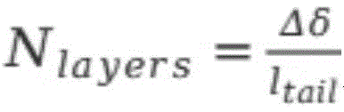
In the embodiment of the present invention, the step S8 may adopt a tail chain length method, and specifically may include the following steps:
according to
Calculating the surface adsorption layer number of the silicon dioxide chip sensor, wherein N
layersFor the number of surface adsorption layers, /)
tailIs the molecular tail length of the surfactant.
In the embodiment of the invention, the silicon dioxide chip sensor can be a silicon dioxide-based quartz crystal chip sensor, the thickness of the quartz crystal chip sensor is 0.3 mu m, and the area of the quartz crystal chip sensor is 0.2cm2The fundamental resonance frequency is 5 MHz. For example, quartz crystal chip sensors are available from Biolin Scientific.
In the embodiment of the present invention, the first injection liquid may be deionized water or a salt solution, and the concentration of the salt solution may range from 1 to 100 mM/L. The salt solution concentration may be determined based on the salt tolerance of the surfactant.
In the embodiment of the present invention, the second injection liquid may be a pure surfactant solution or a mixed solution of a surfactant solution and a salt. In one example, the salt solubility in the mixed solution may be the same as that of the first injection solution. In one example, the second injection may be a 0.02 wt% solution of Sodium Dodecyl Benzene Sulfonate (SDBS) at the critical micelle concentration of the SDBS surfactant.
In the embodiment of the present invention, the first injection liquid is injected again in step S5 in order to desorb the surfactant adsorbed on the surface of the quartz crystal wafer in the second injection liquid.
In the embodiment of the present invention, the flow rate of the first injection liquid or the second injection liquid may be 200 μ L/min, and the operating temperature may be 25 ℃.
In an embodiment of the present invention, the method further includes:
a cleaning step after the end of step S5, the cleaning step including:
flushing the whole system with deionized water at a constant flow rate of 200 μ L/min, wherein the system comprises the flow cell and a connecting pipeline;
washing the quartz crystal chip sensor with deionized water, ethanol and isopropanol for 3 times respectively, and then soaking in isopropanol for two hours;
taking out the quartz crystal chip sensor, and placing the quartz crystal chip sensor in pure and stable nitrogen flow for medium temperature and drying;
the quartz crystal chip sensor is accommodated, for example, the quartz crystal chip sensor can be retracted into the box. In one example, to ensure stability and accuracy of the chip sensor, each chip is used no more than five times.
In an embodiment of the present invention, the first time period may be 10 minutes, and the second time period may be 5 minutes.
In the embodiment of the invention, each layer covers the whole active area of the quartz crystal chip sensor, each layer has a uniform adsorption thickness, each layer is homogeneous, the viscoelastic characteristics of all the layers can be described by a Voigt model expression, the medium of the sensor resonance is Newtonian fluid, and all the layers are stress-free, namely all the layers do not contain internal stress. In an example, the analytical model performing the above method may be a smartfit model.
The method of embodiments of the present invention and the benefits thereof are further elucidated below with reference to a specific example and with reference to fig. 2 to 6.
Monitoring the adsorption quantity of SDBS on the surface of the quartz crystal chip under each frequency multiplication
(1) A silicon dioxide chip sensor is selected, the thickness of the chip sensor is 0.3 mu m, and the area of the chip sensor is 0.2cm2The fundamental resonance frequency is 5 MHz. To eliminate surface contamination, the sensor chip was rinsed 3 times with deionized water, ethanol, and isopropanol in sequence before each measurement. Subsequently, the sensor chip was warmed and dried in a clean nitrogen stream. Placing the sensor chip into a flow cell, connecting a pipeline, setting the temperature at 25 ℃, firstly introducing a first injection liquid (injection liquid 1), namely deionized water, stabilizing for half an hour, reopening a working page and continuously introducing the deionized water to obtain a base line f0。
(2) Waiting for baseline f0After stabilization for five minutes, a second injection (injection 2) was introduced, injection 2 being a 0.02 wt% solution of Sodium Dodecylbenzenesulfonate (SDBS) at the critical micelle concentration of the SDBS surfactant.
(3) Adsorption curve f1And after the silicon dioxide chip is stabilized for five minutes, the injection liquid 1, namely deionized water is introduced again, and the purpose of introducing the deionized water again is to remove SDBS molecules previously adsorbed on the surface of the silicon dioxide chip due to the hydrophilicity of the SDBS, so that the adsorption curve returns to the base line again, and the data are stored. The measurements were repeated 2-4 times for each solution to ensure the accuracy and reliability of the data obtained. After each experiment, the quartz chip sensor is flushed as in step (1), and the flow-through module and connecting tube of the QCM-D also need to be cleaned, following the same procedure as for flushing the quartz chip sensor.
(4) The data was processed using QSenseDfind analysis software to derive a data table of adsorption curves at each frequency doubling and processed in origin software, as shown in fig. 2 and 3. Taking viscoelasticity of the adsorption film into consideration, smartfit is selected for analysis, and a Voigt model is tested by selecting 3 rd to 11 th frequency multiplication so as to obtain adsorption quality and adsorption layer thickness. Selecting the frequency of 1-3.5 minutes as f0And the frequency of 7 to 9.5 minutes is f1F for frequency multiplication of 3 to 110、f1Fitting to obtain chi-square (chi-square)2) The value is about 0.1, indicating a perfect fit with the Voigt model. The calculated mass and thickness were respectively, am 941.46ng/c2And Δ δ of 9.41nm, adsorption mass and thickness maps were made in origin as shown in fig. 4 and 5.
(5) Based on the adsorption mass Δ m and the adsorption thickness Δ δ obtained in step (4), the number of layers of the surfactant adsorbed on the rock surface can be roughly predicted, and the prediction can be performed by three different methods.
First area method
One possible way to estimate the number of adsorbed layers is to obtain the number of single-layer surfactant molecules per unit area from the area a of the surfactant head group, the head group of the SDBS molecule consisting of a sulfonate group. Assuming that the molecular head is a perfect sphere, the head area of the SDBS molecule is approximately 0.54 × 10⁻¹⁴cm2The molecular weight of the monolayer adsorption can be obtained, and the number of adsorbed layers can be obtained by dividing the total mass adsorbed on the surface of the chip by the mass adsorbed by the monolayer. Since this method ignores the presence of a higher density of favorable adsorption sites, the number of layers adsorbed may be overestimated.
Single-layer adsorption capacity of the surface of the quartz crystal chip:
total amount of adsorption on the surface of the quartz crystal chip:
the number of adsorption layers:
adsorption site method
The adsorption site method is used for analyzing the SDBS adsorption sites on the surface of the quartz crystal chipThe number of the point density is assumed to be the same as that of single-layer adsorbed molecules, the number of the molecules per unit area is the number of adsorption sites on the surface of the quartz crystal chip per unit area, and the number of the adsorption sites per unit area of the quartz crystal chip is nmonolayer=5*1014(monolayer/cm2) And the total amount of molecules adsorbed by the unit area of the surface of the chip can be used for obtaining the number of adsorbed layers. The method considers that the surface active agent is very sensitive to adsorption sites, and the implicit assumption in the method is that all the adsorption sites are occupied, wherein the ratio of the surface active agent to the sites is 1:1, so that the estimation of the number of monolayer molecules is higher and the estimation of the number of adsorption layers on the surface of the rock chip is lower.
Total amount of adsorption on the surface of the quartz crystal chip:
the number of the adsorption layers on the surface of the rock chip is as follows:
length method of tail chain
The last method for predicting the number of adsorbed layers is to correlate the thickness of a monolayer with the length of the surfactant tail, and to determine the surfactant tail length by building the surfactant molecules in the Materials studio software, with the SDBS molecule tail length being about ltallApproximately 1.8nm, the adsorption thickness Δ δ can be obtained from (2), which considers the surfactant tail to be fully extended (not folded upon itself), ignoring possible oblique bending of the tail, and therefore the number of adsorbed layers can also be overestimated.
The number of the adsorption layers on the surface of the rock chip is as follows:
the method of the embodiment of the invention predicts the number of the adsorption layers of the surfactant through three different angles, the adsorption model configuration diagram is shown as figure 6, and in a surfactant-water-rock system, the adsorption process of the surfactant is mainly carried out through the electrostatic interaction between the hydrophilic head group of the surfactant and the charged part on the surface of the rock. When the surfactant is coated on the surface of silica in a single layer, hydrophobic chains of the surfactant are exposed to water, which results in an imbalance in adsorption energy, which can be overcome by the interaction of tail chains to form a double-layer structure, and thus the number of layers formed is mostly double-layers.
Compared with the prior art, the embodiment of the invention has the following advantages and effects:
1. the embodiment of the invention provides a novel method for dynamically monitoring the adsorption behavior of surfactant molecules on the solid surface by using a quartz crystal microbalance technology, which is analyzed from three angles (head group area, adsorption sites and tail chain length), has the advantages of comprehensive analysis, simple and convenient algorithm, capability of monitoring the dynamic adsorption behavior in real time and the like, and can provide a good theoretical basis for developing more economical and efficient surfactants and increasing the oil displacement efficiency in China.
2. The embodiment of the invention provides a method for calculating the number of the adsorption layers of the surfactant on the rock surface from three angles of the head base area, the tail chain length and the rock surface adsorption site of the surfactant, researches the adsorption behavior of the rock surface surfactant from the nanogram scale, and provides a reliable theoretical basis for researching more efficient and more economic surfactants.
As will be appreciated by one skilled in the art, embodiments of the present application may be provided as a method, system, or computer program product. Accordingly, the present application may take the form of an entirely hardware embodiment, an entirely software embodiment or an embodiment combining software and hardware aspects. Furthermore, the present application may take the form of a computer program product embodied on one or more computer-usable storage media (including, but not limited to, disk storage, CD-ROM, optical storage, and the like) having computer-usable program code embodied therein.
The present application is described with reference to flowchart illustrations and/or block diagrams of methods, apparatus (systems), and computer program products according to embodiments of the application. It will be understood that each flow and/or block of the flow diagrams and/or block diagrams, and combinations of flows and/or blocks in the flow diagrams and/or block diagrams, can be implemented by computer program instructions. These computer program instructions may be provided to a processor of a general purpose computer, special purpose computer, embedded processor, or other programmable data processing apparatus to produce a machine, such that the instructions, which execute via the processor of the computer or other programmable data processing apparatus, create means for implementing the functions specified in the flowchart flow or flows and/or block diagram block or blocks.
These computer program instructions may also be stored in a computer-readable memory that can direct a computer or other programmable data processing apparatus to function in a particular manner, such that the instructions stored in the computer-readable memory produce an article of manufacture including instruction means which implement the function specified in the flowchart flow or flows and/or block diagram block or blocks.
These computer program instructions may also be loaded onto a computer or other programmable data processing apparatus to cause a series of operational steps to be performed on the computer or other programmable apparatus to produce a computer implemented process such that the instructions which execute on the computer or other programmable apparatus provide steps for implementing the functions specified in the flowchart flow or flows and/or block diagram block or blocks.
In a typical configuration, a computing device includes one or more processors (CPUs), input/output interfaces, network interfaces, and memory.
The memory may include forms of volatile memory in a computer readable medium, Random Access Memory (RAM) and/or non-volatile memory, such as Read Only Memory (ROM) or flash memory (flash RAM). The memory is an example of a computer-readable medium.
Computer-readable media, including both non-transitory and non-transitory, removable and non-removable media, may implement information storage by any method or technology. The information may be computer readable instructions, data structures, modules of a program, or other data. Examples of computer storage media include, but are not limited to, phase change memory (PRAM), Static Random Access Memory (SRAM), Dynamic Random Access Memory (DRAM), other types of Random Access Memory (RAM), Read Only Memory (ROM), Electrically Erasable Programmable Read Only Memory (EEPROM), flash memory or other memory technology, compact disc read only memory (CD-ROM), Digital Versatile Discs (DVD) or other optical storage, magnetic cassettes, magnetic tape magnetic disk storage or other magnetic storage devices, or any other non-transmission medium that can be used to store information that can be accessed by a computing device. As defined herein, a computer readable medium does not include a transitory computer readable medium such as a modulated data signal and a carrier wave.
It should also be noted that the terms "comprises," "comprising," or any other variation thereof, are intended to cover a non-exclusive inclusion, such that a process, method, article, or apparatus that comprises a list of elements does not include only those elements but may include other elements not expressly listed or inherent to such process, method, article, or apparatus. Without further limitation, an element defined by the phrase "comprising an … …" does not exclude the presence of other identical elements in the process, method, article, or apparatus that comprises the element.
The above are merely examples of the present application and are not intended to limit the present application. Various modifications and changes may occur to those skilled in the art. Any modification, equivalent replacement, improvement, etc. made within the spirit and principle of the present application should be included in the scope of the claims of the present application.