CN114088216A - Optical framing camera and method for measuring laser spot change condition in single pulse - Google Patents
Optical framing camera and method for measuring laser spot change condition in single pulse Download PDFInfo
- Publication number
- CN114088216A CN114088216A CN202111282342.3A CN202111282342A CN114088216A CN 114088216 A CN114088216 A CN 114088216A CN 202111282342 A CN202111282342 A CN 202111282342A CN 114088216 A CN114088216 A CN 114088216A
- Authority
- CN
- China
- Prior art keywords
- light
- sample
- reflector array
- detected
- spot
- Prior art date
- Legal status (The legal status is an assumption and is not a legal conclusion. Google has not performed a legal analysis and makes no representation as to the accuracy of the status listed.)
- Granted
Links
Images


Classifications
-
- G—PHYSICS
- G01—MEASURING; TESTING
- G01J—MEASUREMENT OF INTENSITY, VELOCITY, SPECTRAL CONTENT, POLARISATION, PHASE OR PULSE CHARACTERISTICS OF INFRARED, VISIBLE OR ULTRAVIOLET LIGHT; COLORIMETRY; RADIATION PYROMETRY
- G01J11/00—Measuring the characteristics of individual optical pulses or of optical pulse trains
Landscapes
- Physics & Mathematics (AREA)
- General Physics & Mathematics (AREA)
- Spectroscopy & Molecular Physics (AREA)
- Investigating Or Analysing Materials By Optical Means (AREA)
Abstract
The invention belongs to the field of nonlinear optics, and discloses an optical framing camera and a method for measuring laser spot change conditions in a single pulse. Two beams of laser are adopted, one beam of laser is used as pumping light, the other beam of laser is used as detection light, the detection light passes through a convergent step reflector array and then is overlapped on a material at the position of the material, and the pumping light is converged on the material by an imaging system. The convergent step reflector array is composed of a plurality of reflecting surfaces, each reflecting surface is a plane mirror, the reflecting angle of each reflecting surface is different, each beam of reflected light can be overlapped at the same certain position finally, and a certain height difference exists between the steps of each reflecting surface. By means of the convergent step reflector array, one beam of detection light is divided into a plurality of detection light pulse sequences with time delay difference, and the law of spatial distribution change of the pumping light spot in one pulse can be obtained, so that ultra-fast imaging is achieved, and the imaging speed can reach fs level.
Description
Technical Field
The invention relates to a nonlinear optical physical mechanism for researching materials and a single-pulse ultrafast imaging device, belonging to the field of nonlinear optics.
Background
The birth of transient optical imaging technology dates back to the 70 th 19 th century, where the U.S. photographers e.muybridge initiated the initiative by capturing horses in motion. Today over a century ago, scientists have been able to achieve femtosecond laser-induced lattice vibration wave imaging with a single exposure. This allows the ultra-fast imaging technique of single exposure to have irreplaceable advantages in the face of irreversible measurements of optical megawaves, irreversible structure dynamics in chemical reactions, and shock wave generation in inertial confinement nuclear fusion.
When some irreversible dynamics phenomena are subjected to ultrafast imaging, the traditional pump detection technology obviously cannot meet the measurement requirement, because the time delay of two beams of pulse light is realized through a mobile platform, and spot images of the pump light under different time delays can be obtained after the repeated action of a plurality of pulses, the images changing along with time in one pulse are not really measured. In addition, the problems of multiple measurement and time jitter exist in the traditional ultrafast electronic imaging technology. A single pulse imaging technique is therefore required to solve the above problem.
Disclosure of Invention
The invention solves the problem of measuring a laser single-pulse ultrafast time-resolved and space-resolved imaging, and provides an optical framing camera, which comprises: the device comprises an incident detection laser beam, a beam splitter, a convergent stepped reflector array, an incident pumping laser beam, a sample frame, an imaging system, a compensation stepped reflector array and a CCD (charge coupled device); after penetrating through the beam splitter, the detection light emitted by the incident detection laser beam is reflected to the beam splitter by the convergent step mirror array, and then the detection light is reflected to a sample to be detected at the sample rack by the rear surface of the beam splitter; meanwhile, pump light emitted by the incident pump laser beam is also incident to a sample to be detected, and the probe light passing through the sample to be detected is converged by the imaging system, reflected by the compensating step reflector array and imaged in the CCD; the convergent step reflector array and the compensating step reflector array are both composed of a plurality of reflecting surfaces, each reflecting surface is a plane mirror, the reflecting angle of each reflecting surface is different, each beam of reflected light is finally overlapped at the same position, and a certain height difference exists between the steps of each reflecting surface.
The working principle of the technical scheme is as follows: after light emitted by an incident detection laser beam penetrates through a beam splitter and is reflected by a convergent step reflector array, a beam of detection light is divided into a plurality of detection light pulse sequences with time delay difference, the detection light and pump light are overlapped at a sample to be detected, meanwhile, the pump light acts on any position in a detection light range, after the pump light acts on the sample to be detected, the pump light acts on the sample to be detected at different moments in a pulse in different ways, therefore, the distribution condition of light spots of the pump light at different moments is recorded by the detection light, and after the detection light sequences pass through the sample to be detected, the detection light sequences pass through an imaging system and a compensating step reflector array and are finally imaged in a CCD.
Because the converging step mirror array is distributed in a step shape, after the detection light transmits through each step, different optical path differences can be generated between the transmitted light beams, and therefore time delay can be generated between each light beam. The reflected light beams of each reflecting mirror surface are directly reflected to the position of the sample to be measured in parallel according to a certain angle, and the reflected light beams of all the reflecting mirror units are overlapped at the position of the sample to be measured. After the pump light acts on the sample to be detected, because the population numbers of particles at different positions of the sample to be detected are related to the excitation light intensity and continuously change along with time, if the light intensity distribution at different positions in the pump light beam is different, the corresponding detection light spots can be generated in the light spot images corresponding to the pump light. Meanwhile, because steps exist among the reflector units, the influence of the reflected detection light at different moments is different, the light intensity distribution conditions of the pump light at different moments can be known from the intensity change of the pump light region in the detection light beam of the sample to be detected, and the change condition of the light spot of the pump light in a single pump light pulse can be obtained by analyzing the light intensity distribution conditions of the pump light at different moments. The law of the spatial distribution change of the pumping light spots in one pulse can be obtained, so that ultra-fast imaging is realized, and the imaging speed can reach fs level.
A better scheme is as follows: and the pumping light and the detection light are overlapped at the sample to be detected, and the spot size of the pumping light at the sample to be detected is smaller than that of the detection light.
The further scheme is as follows: any reflecting surface on the compensating stepped reflecting mirror array is complementary with a corresponding reflecting surface on the converging stepped reflecting mirror array in angle, and the overall shape formed by all the reflecting surfaces on the compensating stepped reflecting mirror array is complementary with the overall shape formed by all the reflecting surfaces on the converging stepped reflecting mirror array.
Preferably: the overall shape formed by each reflecting surface on the compensating step reflector array is convex, and the overall shape formed by each reflecting surface on the converging step reflector array is concave.
The further scheme is as follows: the convex height of each reflecting surface on the compensating step reflector array is equal to the concave depth of the corresponding reflecting surface on the converging step reflector array.
The steps of measuring by the scheme are as follows:
1) a sample to be detected is not placed on the sample frame, and light spots reflected by the convergent step reflector array are received by the CCD; the light spot received by the CCD is a detection light background spot;
2) placing a sample to be detected on the sample frame, and receiving light spots reflected by the convergent step mirror array and penetrating through the sample to be detected by using a CCD (charge coupled device), wherein the light spots received by the CCD are light spots with pump light spot space distribution;
3) and processing the two obtained light spots to obtain a light spot change image of the required pump light in one pulse.
It is worth mentioning that: the step (1) and the step (2) have no sequence, and the same effect can be realized by interchanging. Or the light path is divided into two same light paths by using the beam splitter, one light path is used for placing the sample to be detected, and the other light path is not used for placing the sample to be detected. And the two light spots are imaged in a CCD at the same time.
In the above technical solution, the detection light path may be a lens imaging system or a 4f imaging system. In the lens imaging system, a sample to be measured is placed on an object plane of a convergent lens, and a CCD is placed on an image plane of the convergent lens. For a 4f imaging system, the sample to be measured is placed in the object plane of the system and the CCD is placed in the image plane of the system.
In the above technical solution, in the step (1), when the sample to be detected is not placed, the CCD receives a light spot of the probe light, which is a background light spot.
In the above technical solution, the step (2) is to place the sample to be detected in the detection light path, and the CCD receives the light spot of the detection light, including the spatial distribution information of the pump light spot;
in the above technical solution, the processing in step 3) includes subtracting the background image in step 1) from the spot image in step 2), and then subtracting the previous pulse image from the next pulse image according to the sequence of the delay time of the pulse sequence, so as to finally obtain the distribution of the spots of the pulsed light in the single pulse at different times.
In the above technical scheme, the step reflector array in step (1) is of a concave-like structure, a certain height difference exists between steps of each reflecting surface, and the light reflected by each reflecting surface can coincide the sequence of the reflected light beams at the position of the sample to be measured.
In the above technical solution, in the novel optical framing camera device in step (1), the imaging system behind the sample to be measured is an imaging lens, the sample to be measured is placed on an object plane of the imaging system, and the CCD is placed on an image plane of the imaging system.
In the above technical solution, the step widths of the converging step reflector array and the compensating step reflector array are determined by the size of an image formed in an imaging system, the size of a light spot of the probe light, and the pixel size of the CCD, and the algorithm is that the step width of the converging step reflector array is nxccd pixel size/imaging system magnification, and N is the number of pixels occupied by each plane mirror in the converging step reflector array; the step height of the converging step mirror array is delay time resolution × light speed/2.
In the above technical solution, the obtaining of the light spot containing the pumping light spot information obtained in the step (2) requires that the pumping light coincides with the overlapped probe light sequence beam, and in order to completely display the light spot distribution of the pumping light, the light spot size of the pumping light is smaller than the light spot size of the probe light.
According to the scheme, the situation of light spot space distribution change of single pump light at different moments in a pulse can be obtained, the large-size parallel light spots are overlapped on a sample to be tested at a certain position by establishing the similar concave surface reflection stepped mirror, and the pump light is introduced into the light path and acts on the sample to be tested. The delay time between the strong pump light and the pulse detection light sequence generated by the reflecting stepped mirror is considered, and finally the change of a single pulse pump light spot along with the time is obtained according to the change of the detection light spot along with the time, so that the change condition of the pump light spot at different moments is realized, and the realization of the ultrafast all-optical amplitude-division technology is completed.
Through above-mentioned technical scheme, utilize a brand-new thinking to realize the measurement to the different moments laser facula situation of change in a pulse, compare with other measurement technique, have following advantage:
1. the light path is very simple, and the measurement of the light spot time and the spatial resolution of the laser in one pulse can be obtained only by the aid of the angle step reflector, the lens and the CCD;
2. the imaging speed of ps and even fs level can be finished without expensive CCD;
3. the measurement is very convenient, the movement of a sample to be measured is avoided, and the light spot change condition of the pump light in one pulse can be obtained only by one laser pulse, namely the pump light in a single pulse is obtained;
4. in the method, a high-precision moving platform in a traditional optical path is not needed to realize time delay, and only one time delay step reflector is needed to realize time delay;
5. the method greatly improves the time resolution of measurement compared with the prior gated framing camera (tens of picoseconds) while realizing high space resolution.
Drawings
In order to more clearly illustrate the embodiments of the present invention or the technical solutions in the prior art, the drawings used in the description of the embodiments or the prior art will be briefly described below.
FIG. 1 is a schematic diagram of an optical framing camera;
wherein: 1. the method comprises the steps of incidence detection laser beams, 2, a beam splitter, 3, a convergent step reflector array, 4, incidence pumping laser beams, 5, a sample frame, 6, an imaging system, 7, a compensation step reflector array, 8 and a CCD.
Fig. 2 is a diagram of background light spots of the detection light at different times within a pulse without pumping light.
Fig. 3 is a diagram of the background speckle of the probe light at different times within a pulse when the pump light energy is strong.
FIG. 4 is a schematic diagram of a converging step mirror array configuration in one embodiment.
FIG. 5 is a schematic diagram of an exemplary compensated stepped mirror array.
Detailed Description
The technical solution in the embodiments of the present invention will be clearly and completely described below with reference to the accompanying drawings in the embodiments of the present invention.
As shown in fig. 1, an optical framing camera includes, in order along an optical axis direction: the device comprises an incident detection laser beam 1, a beam splitter 2, a convergent step reflector array 3, an incident pumping laser beam 4, a sample frame 5, an imaging system 6, a compensation step reflector array 7 and a CCD 8; after penetrating through the beam splitter, the detection light emitted by the incident detection laser beam is reflected to the beam splitter by the convergent step mirror array, and then the detection light is reflected to a sample to be detected at the sample rack by the rear surface of the beam splitter; meanwhile, pump light emitted by the incident pump laser beam is also incident to a sample to be detected, and the probe light passing through the sample to be detected is converged by the imaging system, reflected by the compensating step reflector array and imaged in the CCD; the convergent step reflector array and the compensating step reflector array are both composed of a plurality of reflecting surfaces, each reflecting surface is a plane mirror, the reflecting angle of each reflecting surface is different, each beam of reflected light is finally overlapped at the same position, and a certain height difference exists between the steps of each reflecting surface.
In the framing experiment, each reflecting surface of the convergent step reflector array 3 is processed to be 4mm multiplied by 4mm, 3 reflecting units are processed in each row, 3 rows are processed in total, 1mm interval exists between each row and each column, so that 9 reflecting units can be obtained once, 9 pieces of energy of detected light can be obtained after 4f imaging light paths are passed, the step height between each reflecting mirror surface and the reflecting mirror surface is determined according to measurement requirements, the time resolution from the femtosecond level to the picosecond level can be realized, the specific calculation formula is 20 x h/3 picoseconds, and the unit of the height h is millimeter. Different from the common step mirror array, as shown in fig. 4, in the convergent step mirror array, except for a certain time delay between each reflection unit, the reflection angles of each reflection unit are different, and a structure similar to a concave mirror is finally formed, but each reflection unit is a plane mirror. The light reflected by the convergent step reflector array is coincided at a position, the coincided position can be regarded as a focus of the convergent step reflector array, a sample to be detected with an excited state or a carrier with a long service life is placed at the position, the sizes of 9 light spots are guaranteed to be about 4mm multiplied by 4mm due to the fact that the reflected light is incident in parallel, the pump light acts on the sample to be detected, the size of the pump light spot is smaller than that of a detection light spot, and time delay between the pump light pulse and the detection light is adjusted. It should be noted that the visible light reflected by the converging step mirror array cannot be directly imaged on the CCD after passing through the sample to be measured, because all the probe light is overlapped at the position of the observed pump light spot, it is necessary to design a compensating step mirror array as shown in fig. 5, and the structure of the compensating step mirror array and the structure of the converging step mirror array are kept complementary as much as possible. After the reflection of different reflecting surfaces in the compensating step reflector array, originally overlapped images can be separated and finally imaged on the CCD. After image processing, the image of the detection light change caused by the space distribution change of a single pump pulse light spot in the sample area to be detected at different moments can be obtained, and the space distribution change of the detection light spot after the sample to be detected is the change caused by the space energy distribution of the pump light, so that the space distribution image of the pump light single pulse at different moments can be obtained. Two CCDs can be used for simultaneous detection, one is used for monitoring the spatial distribution of the detection light, and the other is used for monitoring the spatial distribution of the detection light after the action of the pump light, so that the measurement precision of the single-pulse light spot time and spatial resolution is improved.
In this embodiment, the laser emits a frequency doubling signal 532nm laser with a pulse width of 21ps, and the CCD is ADIMEC-4020 m. The sample to be measured is zinc selenide (ZnSe), the two-photon absorption optical nonlinearity is adopted at the position of 532nm, the step height of the convergent step reflector array is 300 mu m, and the time resolution is 2 ps.
The specific detection steps are as follows: 1) a sample to be detected is not placed on the sample frame, and light spots reflected by the convergent step reflector array are received by the CCD; the light spot received by the CCD is a detection light background spot; 2) placing a sample to be detected on the sample frame, and receiving light spots which are reflected by the convergent step mirror array and then penetrate through the sample to be detected by using a CCD (charge coupled device), wherein the light spots received by the CCD are light spots with pumping light spot space distribution information; 3) and processing the two obtained light spots to obtain a light spot change image of the required pump light in one pulse.
The specific process of theoretical calculation of the ZnSe optical nonlinearity is as follows:
since the detected light energy is very weak compared to the pump light, two-photon absorption of the pump light becomes the only way for free carrier generation, and its rate can be expressed as:

in the formula IeIs the light intensity, tau, of the pump light at the sample to be measuredrFor free carrier lifetime, the change in absorption coefficient due to free carriers is proportional to the excess carrier concentration and can be expressed as:
Δαf=σαΔN(t) (2)
in the formula sigmaαIn order to absorb the cross section by free carriers, considering the combination of the bound electron effect and the common effect of the free carriers, the thin sample to be detected is approximate to the slow-changing amplitude, and the propagation formula of the detection light and the pump light in the ZnSe crystal is as follows:
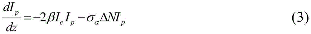

in the formula IpIndicating the intensity of the probe light. Background light spot and pumpThe spot pattern of the pump spot information is shown in fig. 2. When only the detection light acts on the sample to be detected, the nonlinear effect of the material is very weak and basically has no change, and the surrounding detection light passes through the sample to be detected linearly without any change, so that fig. 2 shows that the linear light spot of the laser light spot after passing through the material is the background light spot. When the pump light acts on the sample to be detected, the stronger pump light can excite the sample to be detected to generate nonlinearity, a detection light spot sequence is generated on a step reflector on the sample to be detected, the time delay between the detection light and the pump light is properly adjusted, and the nonlinear mechanism of ZnSe is a transient absorption process of two-photon absorption, so that a rapid absorption process exists in the pulse width time, which is represented by that the light intensity at the position in a light spot image is weaker than that of a linear light spot, and a red square frame is stronger and represents that the pump light at the moment is weaker as a result of subtracting a light spot image containing pump light information from a background light spot image in a figure 3. Each light spot image in fig. 3 is the shape of the pump light spot at a certain time in the pulse, so that the spatial time-resolved change of the pump light spot in a single pulse can be obtained simultaneously by detecting the light spot sequence and the nonlinear sample to be detected.
The previous description of the disclosed embodiments is provided to enable any person skilled in the art to make or use the present invention. Various modifications to these embodiments will be readily apparent to those skilled in the art, and the generic principles defined herein may be applied to other embodiments without departing from the spirit or scope of the invention.
Claims (9)
1. An optical framing camera, comprising: the device comprises an incident detection laser beam, a beam splitter, a convergent stepped reflector array, an incident pumping laser beam, a sample frame, an imaging system, a compensation stepped reflector array and a CCD (charge coupled device);
after penetrating through the beam splitter, the detection light emitted by the incident detection laser beam is reflected to the beam splitter by the convergent step mirror array, and then the detection light is reflected to a sample to be detected at the sample rack by the rear surface of the beam splitter;
meanwhile, pump light emitted by the incident pump laser beam is also incident to a sample to be detected, and the probe light passing through the sample to be detected is converged by the imaging system, reflected by the compensating step reflector array and imaged in the CCD;
the convergent step reflector array and the compensating step reflector array are both composed of a plurality of reflecting surfaces, each reflecting surface is a plane mirror, the reflecting angle of each reflecting surface is different, each beam of reflected light is finally overlapped at the same position, and the height difference exists between every two reflecting surfaces.
2. An optical framing camera as claimed in claim 1, wherein: the imaging system behind the sample to be detected is an imaging lens, the sample to be detected is placed on an object plane of the imaging system, and the CCD is placed on an image plane of the imaging system.
3. An optical framing camera as claimed in claim 1, wherein: the step widths of the convergent step reflector array and the compensating step reflector array are determined by the size of an image formed in an imaging system, the size of a light spot of the detection light and the size of a pixel of the CCD, the algorithm is that the step width of the convergent step reflector array = NxCCD pixel size/imaging system amplification factor, and N is the number of pixels occupied by each plane mirror in the convergent step reflector array; step height of the converging step mirror array = delay time resolution x speed of light/2.
4. An optical framing camera as claimed in claim 1, wherein: and the pumping light and the detection light are overlapped at the sample to be detected, and the spot size of the pumping light at the sample to be detected is smaller than that of the detection light.
5. An optical framing camera as claimed in claim 1, wherein: any reflecting surface on the compensating stepped reflecting mirror array is complementary with a corresponding reflecting surface on the converging stepped reflecting mirror array in angle, and the overall shape formed by all the reflecting surfaces on the compensating stepped reflecting mirror array is complementary with the overall shape formed by all the reflecting surfaces on the converging stepped reflecting mirror array.
6. An optical framing camera as claimed in claim 1, wherein: the overall shape formed by each reflecting surface on the compensating step reflector array is convex, and the overall shape formed by each reflecting surface on the converging step reflector array is concave.
7. An optical framing camera as claimed in claim 6, wherein: the convex height of each reflecting surface on the compensating step reflector array is equal to the concave depth of the corresponding reflecting surface on the converging step reflector array.
8. A method for measuring laser spot change condition in a single pulse is characterized by comprising the following steps: the optical framing camera of any one of claims 1-7, wherein the detection step comprises:
1) a sample to be detected is not placed on the sample frame, and light spots reflected by the convergent step reflector array are received by the CCD; the light spot received by the CCD is a detection light background light spot;
2) placing a sample to be detected on the sample frame, and receiving light spots reflected by the convergent step mirror array and penetrating through the sample to be detected by using a CCD (charge coupled device), wherein the light spots received by the CCD are light spots with pump light spot space distribution;
3) and processing the obtained background light spot and the obtained pumping light spot to obtain a light spot change image of the required pumping light in one pulse.
9. The method for measuring the variation of a laser spot in a single pulse as claimed in claim 8, wherein: the processing in the step 3) includes subtracting the background image in the step 1) from the spot image in the step 2), and then subtracting the previous pulse image from the next pulse image according to the sequence of the delay time of the pulse sequence, so as to finally obtain the distribution condition of the spots of the pulsed light in the single pulse at different times.
Priority Applications (1)
| Application Number | Priority Date | Filing Date | Title |
|---|---|---|---|
| CN202111282342.3A CN114088216B (en) | 2021-11-01 | 2021-11-01 | Optical framing camera and method for measuring laser spot changes within a single pulse |
Applications Claiming Priority (1)
| Application Number | Priority Date | Filing Date | Title |
|---|---|---|---|
| CN202111282342.3A CN114088216B (en) | 2021-11-01 | 2021-11-01 | Optical framing camera and method for measuring laser spot changes within a single pulse |
Publications (2)
| Publication Number | Publication Date |
|---|---|
| CN114088216A true CN114088216A (en) | 2022-02-25 |
| CN114088216B CN114088216B (en) | 2025-02-07 |
Family
ID=80298421
Family Applications (1)
| Application Number | Title | Priority Date | Filing Date |
|---|---|---|---|
| CN202111282342.3A Active CN114088216B (en) | 2021-11-01 | 2021-11-01 | Optical framing camera and method for measuring laser spot changes within a single pulse |
Country Status (1)
| Country | Link |
|---|---|
| CN (1) | CN114088216B (en) |
Cited By (1)
| Publication number | Priority date | Publication date | Assignee | Title |
|---|---|---|---|---|
| CN116107064A (en) * | 2023-04-13 | 2023-05-12 | 西安玄瑞光电科技有限公司 | Single-lens sub-aperture confocal plane optical imaging system |
Citations (7)
| Publication number | Priority date | Publication date | Assignee | Title |
|---|---|---|---|---|
| US3602718A (en) * | 1968-05-31 | 1971-08-31 | Comp Generale Electricite | Means for measuring the duration of very short light pulses,such as laser pulses |
| EP1521111A1 (en) * | 2003-09-30 | 2005-04-06 | Carl Zeiss SMS GmbH | Illumination device |
| JP2010127831A (en) * | 2008-11-28 | 2010-06-10 | Yokohama National Univ | Optical delay element and light pulse measuring instrument |
| CN102620829A (en) * | 2012-04-12 | 2012-08-01 | 重庆大学 | Fourier transform infrared spectrometer based on programmable MEMS (micro-electro-mechanical system) micromirror and single-point detector |
| CN108344563A (en) * | 2018-05-11 | 2018-07-31 | 中国科学院西安光学精密机械研究所 | Reflection type beam division delayer and method for measuring time resolution of framing camera |
| CN110658161A (en) * | 2019-11-12 | 2020-01-07 | 苏州大学 | Ultrashort single-beam single-pulse time-resolved pumping detection device and method and delay ladder window |
| CN216349168U (en) * | 2021-11-01 | 2022-04-19 | 苏州大学 | Optical framing camera |
-
2021
- 2021-11-01 CN CN202111282342.3A patent/CN114088216B/en active Active
Patent Citations (7)
| Publication number | Priority date | Publication date | Assignee | Title |
|---|---|---|---|---|
| US3602718A (en) * | 1968-05-31 | 1971-08-31 | Comp Generale Electricite | Means for measuring the duration of very short light pulses,such as laser pulses |
| EP1521111A1 (en) * | 2003-09-30 | 2005-04-06 | Carl Zeiss SMS GmbH | Illumination device |
| JP2010127831A (en) * | 2008-11-28 | 2010-06-10 | Yokohama National Univ | Optical delay element and light pulse measuring instrument |
| CN102620829A (en) * | 2012-04-12 | 2012-08-01 | 重庆大学 | Fourier transform infrared spectrometer based on programmable MEMS (micro-electro-mechanical system) micromirror and single-point detector |
| CN108344563A (en) * | 2018-05-11 | 2018-07-31 | 中国科学院西安光学精密机械研究所 | Reflection type beam division delayer and method for measuring time resolution of framing camera |
| CN110658161A (en) * | 2019-11-12 | 2020-01-07 | 苏州大学 | Ultrashort single-beam single-pulse time-resolved pumping detection device and method and delay ladder window |
| CN216349168U (en) * | 2021-11-01 | 2022-04-19 | 苏州大学 | Optical framing camera |
Non-Patent Citations (2)
| Title |
|---|
| JUNYI YANG ET AL.: "Single‑shot pump‑probe technique using mirror array", APPLIED PHYSICS B, 5 May 2020 (2020-05-05), pages 1 * |
| 王煜等: "测量光学非线性的4f 相位相干成像技术研究进展", 红外与激光工程, vol. 37, no. 4, 31 August 2008 (2008-08-31), pages 1 * |
Cited By (2)
| Publication number | Priority date | Publication date | Assignee | Title |
|---|---|---|---|---|
| CN116107064A (en) * | 2023-04-13 | 2023-05-12 | 西安玄瑞光电科技有限公司 | Single-lens sub-aperture confocal plane optical imaging system |
| CN116107064B (en) * | 2023-04-13 | 2023-08-22 | 西安玄瑞光电科技有限公司 | Single-lens aperture-dividing confocal plane framing optical imaging system |
Also Published As
| Publication number | Publication date |
|---|---|
| CN114088216B (en) | 2025-02-07 |
Similar Documents
| Publication | Publication Date | Title |
|---|---|---|
| US9912852B2 (en) | Real-time, ultrafast framing optical imaging device with high spatial resolution | |
| CN112902866B (en) | Spatial framing device, all-optical ultrafast imaging system and method | |
| CN101520955B (en) | A Method for Accurately Measuring and Controlling Time Delay of Two Ultrashort Pulse Lasers | |
| CN113900079B (en) | Compensation correction device and method for full-light ultrafast imaging | |
| CN111781629B (en) | X-ray optical framing imaging system | |
| CN104317154A (en) | Ultrafast continuous imaging device and method | |
| CN111443062A (en) | Ultrafast detection device and method for transient refractive index of semiconductor material | |
| CN113514484B (en) | All-optical framing system for X-ray imaging | |
| CN216349168U (en) | Optical framing camera | |
| CN114088216A (en) | Optical framing camera and method for measuring laser spot change condition in single pulse | |
| US11086192B2 (en) | Single shot autocorrelator for measuring the duration of an ultrashort pulse in the far field | |
| CN106454334A (en) | Device for measuring exposure time of X-ray framing camera | |
| CN114965364B (en) | Single-pulse transient nonlinear refractive index measurement device and measurement method | |
| CN116148232A (en) | A full-spectrum fluorescence lifetime rapid measurement device | |
| NO168392B (en) | PHASE CONJUGED REFLECTING MEDIA | |
| CN110837201B (en) | High time resolution framing camera system | |
| CN113433142B (en) | High space-time resolution optical system suitable for X-ray diagnosis | |
| CN117330527B (en) | A measuring device and method for single pulse long delay transient absorption | |
| KR100790707B1 (en) | Dispersion Controlled Confocal Laser Microscope | |
| CN113504634B (en) | Intelligent high-speed scanning method and device for point scanning long-life fluorescence microscopic imaging | |
| Lai | New tubeless nanosecond streak camera based on optical deflection and direct CCD imaging | |
| Lai et al. | Design and field test of a galvanometer deflected streak camera | |
| Sheffield et al. | Particle velocity measurements of laser-induced shock waves using ORVIS | |
| US7528940B2 (en) | System and method for inspecting an object using an acousto-optic device | |
| CN120428506A (en) | A time-domain controllable ultrafast imaging device and method |
Legal Events
| Date | Code | Title | Description |
|---|---|---|---|
| PB01 | Publication | ||
| PB01 | Publication | ||
| SE01 | Entry into force of request for substantive examination | ||
| SE01 | Entry into force of request for substantive examination | ||
| GR01 | Patent grant | ||
| GR01 | Patent grant |