CN114063362B - Two-dimensional liquid crystal laser deflector - Google Patents
Two-dimensional liquid crystal laser deflector Download PDFInfo
- Publication number
- CN114063362B CN114063362B CN202111352579.4A CN202111352579A CN114063362B CN 114063362 B CN114063362 B CN 114063362B CN 202111352579 A CN202111352579 A CN 202111352579A CN 114063362 B CN114063362 B CN 114063362B
- Authority
- CN
- China
- Prior art keywords
- layer
- sub
- liquid crystal
- regions
- upper substrate
- Prior art date
- Legal status (The legal status is an assumption and is not a legal conclusion. Google has not performed a legal analysis and makes no representation as to the accuracy of the status listed.)
- Active
Links
- 239000004973 liquid crystal related substance Substances 0.000 title claims abstract description 63
- 239000000758 substrate Substances 0.000 claims abstract description 42
- 239000011521 glass Substances 0.000 claims abstract description 9
- 239000003292 glue Substances 0.000 claims abstract description 7
- 125000006850 spacer group Chemical group 0.000 claims description 4
- 239000000565 sealant Substances 0.000 claims 1
- 239000002052 molecular layer Substances 0.000 abstract 4
- 239000010410 layer Substances 0.000 description 69
- 230000003287 optical effect Effects 0.000 description 11
- 238000005516 engineering process Methods 0.000 description 9
- 238000010586 diagram Methods 0.000 description 4
- 238000000034 method Methods 0.000 description 4
- 238000002360 preparation method Methods 0.000 description 3
- 101001121408 Homo sapiens L-amino-acid oxidase Proteins 0.000 description 2
- 102100026388 L-amino-acid oxidase Human genes 0.000 description 2
- 101100233916 Saccharomyces cerevisiae (strain ATCC 204508 / S288c) KAR5 gene Proteins 0.000 description 2
- 238000009826 distribution Methods 0.000 description 2
- 238000011160 research Methods 0.000 description 2
- 239000002356 single layer Substances 0.000 description 2
- 239000004997 Liquid crystal elastomers (LCEs) Substances 0.000 description 1
- 239000004988 Nematic liquid crystal Substances 0.000 description 1
- 239000004642 Polyimide Substances 0.000 description 1
- 230000009286 beneficial effect Effects 0.000 description 1
- 238000004891 communication Methods 0.000 description 1
- 239000013078 crystal Substances 0.000 description 1
- 210000002858 crystal cell Anatomy 0.000 description 1
- 238000011161 development Methods 0.000 description 1
- 238000011982 device technology Methods 0.000 description 1
- 230000000694 effects Effects 0.000 description 1
- 230000005684 electric field Effects 0.000 description 1
- AMGQUBHHOARCQH-UHFFFAOYSA-N indium;oxotin Chemical compound [In].[Sn]=O AMGQUBHHOARCQH-UHFFFAOYSA-N 0.000 description 1
- 238000003475 lamination Methods 0.000 description 1
- 239000000463 material Substances 0.000 description 1
- 230000005693 optoelectronics Effects 0.000 description 1
- 230000000737 periodic effect Effects 0.000 description 1
- 238000000206 photolithography Methods 0.000 description 1
- 229920001721 polyimide Polymers 0.000 description 1
- 239000004065 semiconductor Substances 0.000 description 1
- 238000004528 spin coating Methods 0.000 description 1
- 238000013517 stratification Methods 0.000 description 1
Images


Classifications
-
- G—PHYSICS
- G02—OPTICS
- G02F—OPTICAL DEVICES OR ARRANGEMENTS FOR THE CONTROL OF LIGHT BY MODIFICATION OF THE OPTICAL PROPERTIES OF THE MEDIA OF THE ELEMENTS INVOLVED THEREIN; NON-LINEAR OPTICS; FREQUENCY-CHANGING OF LIGHT; OPTICAL LOGIC ELEMENTS; OPTICAL ANALOGUE/DIGITAL CONVERTERS
- G02F1/00—Devices or arrangements for the control of the intensity, colour, phase, polarisation or direction of light arriving from an independent light source, e.g. switching, gating or modulating; Non-linear optics
- G02F1/29—Devices or arrangements for the control of the intensity, colour, phase, polarisation or direction of light arriving from an independent light source, e.g. switching, gating or modulating; Non-linear optics for the control of the position or the direction of light beams, i.e. deflection
- G02F1/291—Two-dimensional analogue deflection
Landscapes
- Physics & Mathematics (AREA)
- Nonlinear Science (AREA)
- General Physics & Mathematics (AREA)
- Optics & Photonics (AREA)
- Liquid Crystal (AREA)
Abstract
本发明公开了一种二维液晶激光偏转器,包括依次叠加的多层器件,每层器件依次包括上基板、液晶分子层和下基板;所述上基板从上到下依次包括上基板玻璃、上ITO导电层和上取向层,下基板从上到下依次包括下取向层、下ITO导电层和下基板玻璃;所述液晶分子层位于上基板与下基板之间,液晶分子层内部喷洒间隔子进行支撑;上基板与下基板边缘通过框胶进行密封分装,并对位贴合固化。本发明可以通过改变子区域在x,y方向上的宽度dx、dy,改变液晶分子层的厚度以及加载电压的大小来调节出射光在x,y方向的偏转角度θx、θy以实现光束的二维空间扫描,具有偏转精度高、响应速度快、驱动控制简单、结构简单的优点。

The invention discloses a two-dimensional liquid crystal laser deflector, which comprises sequentially stacked multilayer devices, and each layer of devices sequentially includes an upper substrate, a liquid crystal molecular layer and a lower substrate; the upper substrate sequentially includes an upper substrate glass, The upper ITO conductive layer and the upper alignment layer, the lower substrate includes the lower alignment layer, the lower ITO conductive layer and the lower substrate glass from top to bottom; the liquid crystal molecular layer is located between the upper substrate and the lower substrate, and the liquid crystal molecular layer is sprayed at interval Substrates are used for support; the edges of the upper substrate and the lower substrate are sealed and sub-packaged by frame glue, and are aligned and solidified. The present invention can adjust the deflection angles θ x , θ y of the outgoing light in the x, y direction by changing the width d x , dy of the sub-region in the x, y direction, changing the thickness of the liquid crystal molecular layer and the magnitude of the applied voltage. Realize the two-dimensional spatial scanning of the beam, and have the advantages of high deflection precision, fast response speed, simple drive control, and simple structure.
Description
技术领域Technical Field
本发明属于液晶光电子器件技术、液晶光学相控阵空间扫描技术领域,具体公开了一种二维液晶激光偏转器。The invention belongs to the fields of liquid crystal optoelectronic device technology and liquid crystal optical phased array space scanning technology, and specifically discloses a two-dimensional liquid crystal laser deflector.
背景技术Background Art
随着激光技术中的激光雷达、空间光通信等研究领域的迅速发展,而激光控制技术是这些领域的核心技术,对光束扫描装置的体积、重量、功耗、响应速度、偏转精度等都有这极为苛刻的要求。现有的激光控制技术可以分为两类:一类是使用机械转动的光学部件的机械式方案,另一类是使用电光或声光调制器件的非机械式方案。目前,液晶光学相控阵是非机械式光束控制技术的主流方案,其核心原理和微波相控阵基本类似,与传统的机械扫描技术相比具有体积小、重量轻、高精度、随机角度偏转、可编程多光束控制、响应快的特点,这些优势使得液晶光学相控阵在相关应用中发挥了独特的技术优势。由于液晶材料本身的限制,导致衍射效率、扫描范围、偏转精度、响应速度等性能不够理想,尤其是应用在二维扫描的情况下,需要进一步的提高扫描性能。由于液晶相控阵用于光束扫描时,响应速度、偏转效率和偏转精度是该项技术的三大关键性能指标,为了满足军用民用等各方面的需求,提高这三大指标一直是研究液晶相控阵技术的重点和难点。With the rapid development of laser radar, space optical communication and other research fields in laser technology, laser control technology is the core technology in these fields, and there are extremely stringent requirements on the volume, weight, power consumption, response speed, deflection accuracy, etc. of the beam scanning device. Existing laser control technologies can be divided into two categories: one is a mechanical solution using mechanically rotating optical components, and the other is a non-mechanical solution using electro-optical or acousto-optic modulation devices. At present, liquid crystal optical phased array is the mainstream solution of non-mechanical beam control technology. Its core principle is basically similar to that of microwave phased array. Compared with traditional mechanical scanning technology, it has the characteristics of small size, light weight, high precision, random angle deflection, programmable multi-beam control, and fast response. These advantages make liquid crystal optical phased array play a unique technical advantage in related applications. Due to the limitations of the liquid crystal material itself, the performance of diffraction efficiency, scanning range, deflection accuracy, response speed, etc. is not ideal, especially in the case of two-dimensional scanning, the scanning performance needs to be further improved. Since response speed, deflection efficiency and deflection accuracy are the three key performance indicators of liquid crystal phased array technology when used for beam scanning, in order to meet the needs of various military and civilian applications, improving these three indicators has always been the focus and difficulty of research on liquid crystal phased array technology.
目前,已有的二维光学相控阵的控制十分复杂且存在偏转精度、响应速度较低等缺点。比如:统的M×N个阵元的二维光学相控阵就需要M×N个独立的控制单元;传统周期性闪耀光栅模型进行二维光束偏转仅可实现有限的偏转角度;目前以发明的一种基于平面相控阵的二维光束扫描方法,但旋转角度会影响二维偏转精度等。At present, the control of the existing two-dimensional optical phased array is very complex and has disadvantages such as low deflection accuracy and response speed. For example, a traditional two-dimensional optical phased array with M×N array elements requires M×N independent control units; the traditional periodic blazed grating model can only achieve a limited deflection angle for two-dimensional beam deflection; a two-dimensional beam scanning method based on a planar phased array has been invented, but the rotation angle will affect the two-dimensional deflection accuracy.
发明内容Summary of the invention
本发明的目的在于克服现有技术的不足,提供一种可以通过改变子区域在x,y方向上的宽度、改变液晶层的厚度以及加载电压的大小来调节出射光在x,y方向的偏转角度θx、θy以实现光束的二维空间扫描,偏转精度高、响应速度快、结构简单的的二维液晶激光偏转器。The object of the present invention is to overcome the shortcomings of the prior art and to provide a two-dimensional liquid crystal laser deflector which can adjust the deflection angles θ x , θ y of the emitted light in the x and y directions by changing the width of the sub-regions in the x and y directions, changing the thickness of the liquid crystal layer and the magnitude of the loaded voltage to achieve two-dimensional spatial scanning of the light beam, and has high deflection accuracy, fast response speed and simple structure.
本发明的目的是通过以下技术方案来实现的:一种二维液晶激光偏转器,包括依次叠加的多层器件,每层器件依次包括上基板、液晶分子层和下基板;The object of the present invention is achieved through the following technical solutions: a two-dimensional liquid crystal laser deflector, comprising a plurality of layers of devices stacked in sequence, each layer of the device comprising an upper substrate, a liquid crystal molecule layer and a lower substrate in sequence;
所述上基板从上到下依次包括上基板玻璃、上ITO导电层和上取向层,下基板从上到下依次包括下取向层、下ITO导电层和下基板玻璃;The upper substrate includes, from top to bottom, an upper substrate glass, an upper ITO conductive layer and an upper alignment layer, and the lower substrate includes, from top to bottom, a lower alignment layer, a lower ITO conductive layer and a lower substrate glass;
所述液晶分子层位于上基板与下基板之间,液晶分子层内部喷洒间隔子进行支撑;The liquid crystal molecule layer is located between the upper substrate and the lower substrate, and spacers are sprayed inside the liquid crystal molecule layer for support;
上基板与下基板边缘通过框胶进行密封分装,并对位贴合固化。The edges of the upper substrate and the lower substrate are sealed and assembled by means of frame glue, and are aligned, fitted and cured.
进一步地,每层器件结构之间通过紫外胶进行逐层对位贴合。Furthermore, each layer of device structure is aligned and bonded layer by layer by ultraviolet glue.
进一步地,二维液晶激光偏转器由三层器件组成,每层器件均为矩形结构,每层器件分为四个矩形子区域ψ1、ψ2、ψ3、ψ4,其中,第一层和第三层四个子区域大小不同,第二层四个子区域大小相同;Further, the two-dimensional liquid crystal laser deflector is composed of three layers of devices, each layer of devices is a rectangular structure, and each layer of devices is divided into four rectangular sub-regions ψ 1 , ψ 2 , ψ 3 , ψ 4 , wherein the four sub-regions of the first layer and the third layer are of different sizes, and the four sub-regions of the second layer are of the same size;
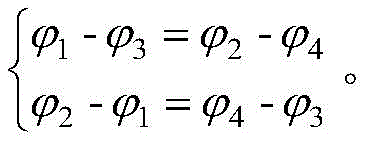
以二维液晶激光偏转器底面的一个顶点为原点,该顶点的三条边分别为x、y、z轴,建立坐标系,z方向包括3个器件结构层;记第二层器件四个子区域的长度和宽度分别为2dx和2dy;将第二层器件的四个区域的交点向x反方向平移dx、y正方向平移dy得到第一层器件四个子区域的交点;将第二层器件的四个子区域的交点向在x正方向平移dx、y反方向平移dy得到第三层器件四个子区域的交点;A coordinate system is established with a vertex of the bottom surface of the two-dimensional liquid crystal laser deflector as the origin, and the three sides of the vertex are respectively the x, y, and z axes, and the z direction includes three device structure layers; the length and width of the four sub-regions of the second layer device are respectively 2d x and 2d y ; the intersection points of the four sub-regions of the second layer device are translated in the opposite direction of x by d x and in the positive direction of y by d y to obtain the intersection points of the four sub-regions of the first layer device; the intersection points of the four sub-regions of the second layer device are translated in the positive direction of x by d x and in the opposite direction of y by d y to obtain the intersection points of the four sub-regions of the third layer device;
四个子区域之间的相位关系满足如下关系式:The phase relationship between the four sub-areas satisfies the following relationship:
进一步地,每层器件的四个子区域加载不同的电压,三个ψ1子区域、ψ2子区域、ψ3子区域和ψ4子区域均加载相同的电压。Furthermore, the four sub-regions of each layer of the device are loaded with different voltages, and the three ψ 1 sub-regions, ψ 2 sub-regions, ψ 3 sub-regions and ψ 4 sub-regions are all loaded with the same voltage.
本发明的有益效果是:本发明可以通过改变子区域在x,y方向上的宽度dx、dy,改变液晶分子层的厚度以及加载电压的大小来调节出射光在x,y方向的偏转角度θx、θy以实现光束的二维空间扫描,具有偏转精度高、响应速度快、驱动控制简单、结构简单的优点。The beneficial effects of the present invention are as follows: the present invention can adjust the deflection angles θ x , θ y of the emitted light in the x, y directions by changing the widths d x , d y of the sub-regions in the x , y directions, changing the thickness of the liquid crystal molecule layer and the magnitude of the loaded voltage to achieve two-dimensional spatial scanning of the light beam, and has the advantages of high deflection accuracy, fast response speed, simple drive control and simple structure.
附图说明BRIEF DESCRIPTION OF THE DRAWINGS
图1为本发明单层器件结构示意图;FIG1 is a schematic diagram of the structure of a single-layer device according to the present invention;
图2为本发明整体结构模型图;Fig. 2 is a diagram of the overall structural model of the present invention;
图3为本发明整体结构的俯视图;FIG3 is a top view of the overall structure of the present invention;
图4为本发明液晶分子折射率椭球模型图。FIG. 4 is a diagram of a refractive index ellipsoid model of a liquid crystal molecule according to the present invention.
具体实施方式DETAILED DESCRIPTION
下面结合附图进一步说明本发明的技术方案。The technical solution of the present invention is further described below in conjunction with the accompanying drawings.
如图1所示,本发明的一种二维液晶激光偏转器,包括依次叠加的多层器件,每层器件依次包括上基板、液晶分子层和下基板;As shown in FIG1 , a two-dimensional liquid crystal laser deflector of the present invention comprises a plurality of layers of devices stacked in sequence, each layer of the device comprising an upper substrate, a liquid crystal molecule layer and a lower substrate in sequence;
所述上基板从上到下依次包括上基板玻璃、上ITO导电层和上取向层,下基板从上到下依次包括下取向层、下ITO导电层和下基板玻璃;The upper substrate includes, from top to bottom, an upper substrate glass, an upper ITO conductive layer and an upper alignment layer, and the lower substrate includes, from top to bottom, a lower alignment layer, a lower ITO conductive layer and a lower substrate glass;
所述液晶分子层位于上基板与下基板之间,液晶分子层内部喷洒间隔子进行支撑,间隔子的直径决定了液晶分子层的厚度;The liquid crystal molecule layer is located between the upper substrate and the lower substrate, and spacers are sprayed inside the liquid crystal molecule layer for support, and the diameter of the spacers determines the thickness of the liquid crystal molecule layer;
上基板与下基板边缘通过框胶进行密封分装,并对位贴合固化。The edges of the upper substrate and the lower substrate are sealed and assembled by means of frame glue, and are aligned, fitted and cured.
每层器件结构之间通过紫外胶进行逐层对位贴合。Each layer of device structure is aligned and bonded layer by layer using ultraviolet glue.
本发明的工作原理为:二维液晶激光偏转器由三层器件组成,每层器件均为矩形结构,每层器件分为四个矩形子区域ψ1、ψ2、ψ3、ψ4,其中,第一层和第三层四个子区域大小不同,第二层四个子区域大小相同;The working principle of the present invention is as follows: the two-dimensional liquid crystal laser deflector is composed of three layers of devices, each layer of devices is a rectangular structure, and each layer of devices is divided into four rectangular sub-areas ψ 1 , ψ 2 , ψ 3 , ψ 4 , wherein the four sub-areas of the first layer and the third layer are of different sizes, and the four sub-areas of the second layer are of the same size;
以二维液晶激光偏转器底面的一个顶点为原点,该顶点的三条边分别为x、y、z轴,建立如图2所示的坐标系,z方向包括3个器件结构层;设期望光束发生在x、y方向上偏转,入射光沿着z方向入射。所述二维液晶激光偏转器由三层器件组成,如图2所示,每个器件结构层内液晶分子层的厚度为Lμm。记第二层器件四个子区域的长度和宽度分别为2dx和2dy;将第二层器件的四个区域的交点向x反方向平移dx、y正方向平移dy得到第一层器件四个子区域的交点;将第二层器件的四个子区域的交点向在x正方向平移dx、y反方向平移dy得到第三层器件四个子区域的交点,如图3所示。本实施例中,第一层器件四个子区域的交点坐标为(dx,3dy),第二层器件四个子区域的交点坐标为(2dx,2dy),第三层器件四个子区域的交点坐标为(3dx,dy),三层器件叠加后形成如图3所示的16个大小相同的子区域,每个子区域x方向宽度为dx,y方向宽度为dy。Take a vertex on the bottom surface of the two-dimensional liquid crystal laser deflector as the origin, and the three sides of the vertex are the x, y, and z axes respectively. Establish a coordinate system as shown in Figure 2, and the z direction includes three device structure layers; assume that the desired light beam is deflected in the x and y directions, and the incident light is incident along the z direction. The two-dimensional liquid crystal laser deflector is composed of three layers of devices, as shown in Figure 2, and the thickness of the liquid crystal molecule layer in each device structure layer is Lμm. Note that the length and width of the four sub-regions of the second layer device are 2d x and 2d y respectively; translate the intersection of the four regions of the second layer device in the opposite direction of x by d x and in the positive direction of y by d y to obtain the intersection of the four sub-regions of the first layer device; translate the intersection of the four sub-regions of the second layer device in the positive direction of x by d x and in the opposite direction of y by d y to obtain the intersection of the four sub-regions of the third layer device, as shown in Figure 3. In this embodiment, the coordinates of the intersection points of the four sub-regions of the first layer of devices are (d x , 3d y ), the coordinates of the intersection points of the four sub-regions of the second layer of devices are (2d x , 2d y ), and the coordinates of the intersection points of the four sub-regions of the third layer of devices are (3d x , dy ). After the three layers of devices are superimposed, 16 sub-regions of the same size are formed as shown in Figure 3 , and each sub-region has a width of d x in the x direction and a width of d y in the y direction.
当对二维液晶激光偏振器施加电压时,由于液晶介电常数和折射率的各向异性,外加电场使得液晶分子的指向矢发生偏转,改变了液晶对非寻常光(e光)的折射率,从而改变了液晶的双折射率,入射光束通过液晶后的光程差因此发生变化。采用精密电路调节加载在液晶分子上的电压值,产生一个固定的相位差,激光通过二维液晶激光偏转器后在x、y方向上发生微小角度偏转从而实现二维空间扫描。When voltage is applied to the two-dimensional liquid crystal laser polarizer, due to the anisotropy of the dielectric constant and refractive index of the liquid crystal, the external electric field causes the director of the liquid crystal molecule to deflect, changing the refractive index of the liquid crystal to extraordinary light (e-light), thereby changing the birefringence of the liquid crystal, and the optical path difference of the incident light beam after passing through the liquid crystal changes. A precision circuit is used to adjust the voltage value loaded on the liquid crystal molecules to produce a fixed phase difference. After passing through the two-dimensional liquid crystal laser deflector, the laser deflects at a small angle in the x and y directions to achieve two-dimensional spatial scanning.
根据液晶弹性体理论,液晶分子偏转角度与驱动电压满足非线性光系,根据液晶的电控双折射效应,液晶是单轴晶体,其光轴在液晶分子长轴方向,液晶的折射率椭球是一个分子长轴为旋转轴的椭球,如图4所示,


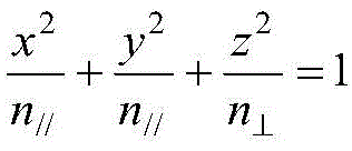

式中n⊥=nx=ny,n//=nz。In the formula, n ⊥ =n x = ny , n // =n z .
光经过第一层器件四个子区域之后的相位调制量分别为:The phase modulation amounts of light after passing through the four sub-regions of the first layer device are:
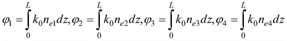
式中
并且四个子区域之间的相位关系满足如下关系式:And the phase relationship between the four sub-areas satisfies the following relationship:

第二层与第三层器件四个子区域加载的相位与第一层相同,每层四个子区域相位都满足上面的关系式。最后三层器件叠加形成图3所示的16个相位分布。The phases loaded in the four sub-regions of the second and third layers of devices are the same as those in the first layer, and the phases of the four sub-regions in each layer satisfy the above relationship. The last three layers of devices are superimposed to form the 16 phase distributions shown in Figure 3.
通过二维液晶激光偏转器后,x方向相邻两个子区域对应的相位延迟量变化差值为:After passing through the two-dimensional liquid crystal laser deflector, the difference in phase delay between two adjacent sub-regions in the x direction is:

因为每层加载相同的相位,此处的

同理,y方向相邻两个子区域对应的相位延迟量变化差值为:Similarly, the difference in phase delay between two adjacent sub-regions in the y direction is:
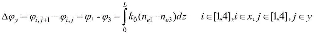
对应的出射光在x方向和y方向的偏转角度θx、θy的变化公式为:The corresponding formulas for the changes in the deflection angles θ x and θ y of the emitted light in the x and y directions are:

因此可以通过改变子区域在x,y方向上的宽度dx、dy,改变液晶分子层的厚度以及加载电压的大小来调节出射光在x,y方向的偏转角度θx、θy以实现光束的二维空间扫描。Therefore, the deflection angles θ x and θ y of the emitted light in the x and y directions can be adjusted by changing the widths d x and dy of the sub-regions in the x and y directions, the thickness of the liquid crystal molecule layer and the magnitude of the applied voltage to achieve two-dimensional spatial scanning of the light beam.
每层器件的四个子区域加载不同的电压,三个ψ1子区域、ψ2子区域、ψ3子区域和ψ4子区域均加载相同的电压。本发明的二维液晶激光偏转器制备过程为:Different voltages are applied to the four sub-regions of each layer of the device, and the same voltage is applied to the three ψ 1 sub-regions, ψ 2 sub-regions, ψ 3 sub-regions and ψ 4 sub-regions. The preparation process of the two-dimensional liquid crystal laser deflector of the present invention is as follows:
(1)制备偏转器电极结构。采用标准的半导体光刻工艺方法,在ITO(氧化铟锡)基板玻璃上按照图3所示的结构图,制备对应的电极图形,电极缝隙为b。(1) Preparation of deflector electrode structure: Using standard semiconductor photolithography process, a corresponding electrode pattern is prepared on an ITO (indium tin oxide) substrate glass according to the structure diagram shown in FIG3 , and the electrode gap is b.
(2)制备单层器件。采用向列相型液晶器件的标准工艺方法和参数工艺参数,包括:旋涂PI(聚酰亚胺)并固化、取向、贴合、灌晶。(2) Preparation of single-layer devices: Standard process methods and parameters for nematic liquid crystal devices are used, including spin coating of PI (polyimide) and curing, orientation, lamination, and filling.
(3)贴合液晶偏转器件。利用紫外胶将制备的三个器件进行逐层对位贴合。(3) Bonding the liquid crystal deflection device. Use ultraviolet glue to align and bond the three prepared devices layer by layer.
本领域的普通技术人员将会意识到,这里所述的实施例是为了帮助读者理解本发明的原理,应被理解为本发明的保护范围并不局限于这样的特别陈述和实施例。本领域的普通技术人员可以根据本发明公开的这些技术启示做出各种不脱离本发明实质的其它各种具体变形和组合,这些变形和组合仍然在本发明的保护范围内。Those skilled in the art will appreciate that the embodiments described herein are intended to help readers understand the principles of the present invention, and should be understood that the protection scope of the present invention is not limited to such specific statements and embodiments. Those skilled in the art can make various other specific variations and combinations that do not deviate from the essence of the present invention based on the technical revelations disclosed by the present invention, and these variations and combinations are still within the protection scope of the present invention.
Claims (3)

Priority Applications (1)
| Application Number | Priority Date | Filing Date | Title |
|---|---|---|---|
| CN202111352579.4A CN114063362B (en) | 2021-11-16 | 2021-11-16 | Two-dimensional liquid crystal laser deflector |
Applications Claiming Priority (1)
| Application Number | Priority Date | Filing Date | Title |
|---|---|---|---|
| CN202111352579.4A CN114063362B (en) | 2021-11-16 | 2021-11-16 | Two-dimensional liquid crystal laser deflector |
Publications (2)
| Publication Number | Publication Date |
|---|---|
| CN114063362A CN114063362A (en) | 2022-02-18 |
| CN114063362B true CN114063362B (en) | 2023-04-07 |
Family
ID=80272886
Family Applications (1)
| Application Number | Title | Priority Date | Filing Date |
|---|---|---|---|
| CN202111352579.4A Active CN114063362B (en) | 2021-11-16 | 2021-11-16 | Two-dimensional liquid crystal laser deflector |
Country Status (1)
| Country | Link |
|---|---|
| CN (1) | CN114063362B (en) |
Families Citing this family (1)
| Publication number | Priority date | Publication date | Assignee | Title |
|---|---|---|---|---|
| CN115167057A (en) * | 2022-06-22 | 2022-10-11 | 电子科技大学 | Transmission-type two-dimensional liquid crystal spatial light modulator |
Citations (1)
| Publication number | Priority date | Publication date | Assignee | Title |
|---|---|---|---|---|
| CN105938274A (en) * | 2016-06-12 | 2016-09-14 | 合肥工业大学 | Deflection film design method and liquid crystal display device |
Family Cites Families (25)
| Publication number | Priority date | Publication date | Assignee | Title |
|---|---|---|---|---|
| US6169594B1 (en) * | 1998-08-24 | 2001-01-02 | Physical Optics Corporation | Beam deflector and scanner |
| US6619799B1 (en) * | 1999-07-02 | 2003-09-16 | E-Vision, Llc | Optical lens system with electro-active lens having alterably different focal lengths |
| US7038835B2 (en) * | 2002-05-28 | 2006-05-02 | Ricoh Company, Ltd. | Optical deflection device and optical deflection method that control occurrence of alignment defect |
| JP4165337B2 (en) * | 2003-08-18 | 2008-10-15 | セイコーエプソン株式会社 | Liquid crystal display device and electronic device |
| KR101286529B1 (en) * | 2007-05-18 | 2013-07-17 | 엘지디스플레이 주식회사 | Liquid Crystal Display Device |
| US8111338B2 (en) * | 2007-09-20 | 2012-02-07 | Koninklijke Philips Electronics N.V. | Beam shaping device |
| BRPI0911394A2 (en) * | 2008-04-25 | 2016-01-05 | Sharp Kk | liquid crystal display device |
| CN103792740B (en) * | 2008-06-06 | 2017-12-12 | 兰斯维克托公司 | Tunable liquid crystal optical device |
| CN101923253B (en) * | 2010-07-29 | 2012-07-11 | 昆山龙腾光电有限公司 | Liquid crystal display panel and liquid crystal display device |
| US9658369B2 (en) * | 2011-05-12 | 2017-05-23 | Sota Shimizu | Geometric transformation lens |
| CN103748509B (en) * | 2011-08-10 | 2016-01-27 | 夏普株式会社 | LCD panel |
| US11194224B2 (en) * | 2013-03-15 | 2021-12-07 | Wavefront Research, Inc. | Low power compact optical communication and collision avoidance systems |
| KR102144733B1 (en) * | 2013-12-30 | 2020-08-18 | 엘지디스플레이 주식회사 | Stereopsis image display device |
| US9939700B2 (en) * | 2014-04-15 | 2018-04-10 | Boe Technology Group Co., Ltd. | Display panel and display apparatus |
| US20160217399A1 (en) * | 2015-01-22 | 2016-07-28 | Elementum Scm (Cayman) Ltd. | Method and system for monitoring shipments in a supply and/or logistics chain |
| JP6441098B2 (en) * | 2015-02-02 | 2018-12-19 | 日東電工株式会社 | Video display mirror for vehicles |
| CN104865768B (en) * | 2015-05-11 | 2018-01-12 | 电子科技大学 | Laser coherent combining method based on two-dimentional liquid crystal optical phased array array |
| CN108107572B (en) * | 2016-11-25 | 2020-07-14 | 中强光电股份有限公司 | near-eye display device |
| CN106959547B (en) * | 2017-03-09 | 2019-08-16 | 苏州晶萃光学科技有限公司 | A kind of liquid crystal beam deviation and scanner and method |
| JP6953754B2 (en) * | 2017-03-17 | 2021-10-27 | 凸版印刷株式会社 | Laser scanning device |
| CN109239993B (en) * | 2018-10-18 | 2021-03-26 | 华北水利水电大学 | A liquid crystal optical switch for optical phased array scanning |
| EP3644119B1 (en) * | 2018-10-26 | 2024-07-10 | Liqxtal Technology Inc. | Liquid crystal phase modulation device and method for fabricating the same |
| CN109343291A (en) * | 2018-12-17 | 2019-02-15 | 电子科技大学 | A liquid crystal laser steering device |
| TWI699592B (en) * | 2019-04-17 | 2020-07-21 | 友達光電股份有限公司 | Display apparatus |
| CN112946966B (en) * | 2021-02-03 | 2023-03-14 | 电子科技大学 | Large-angle liquid crystal optical phased array scanning assembly |
-
2021
- 2021-11-16 CN CN202111352579.4A patent/CN114063362B/en active Active
Patent Citations (1)
| Publication number | Priority date | Publication date | Assignee | Title |
|---|---|---|---|---|
| CN105938274A (en) * | 2016-06-12 | 2016-09-14 | 合肥工业大学 | Deflection film design method and liquid crystal display device |
Also Published As
| Publication number | Publication date |
|---|---|
| CN114063362A (en) | 2022-02-18 |
Similar Documents
| Publication | Publication Date | Title |
|---|---|---|
| CN108508506A (en) | Dual-function device combining wave plate and optical device based on medium super surface | |
| US20150002794A1 (en) | Substrate with spacer and liquid crystal cell containing the same | |
| CN111273467A (en) | Terahertz wave front phase control device based on liquid crystal and wire grid-shaped super-structure surface | |
| CN113820895A (en) | A pixelated dynamic holographic display device based on metasurface and its realization method | |
| Nys et al. | Nematic liquid crystal disclination lines driven by a photoaligned defect grid | |
| CN114326226A (en) | An Electrically Addressable Metasurface for Terahertz Wavefront Modulation | |
| CN113325651B (en) | Liquid crystal optical phased array thermal lens effect compensation device, system and method | |
| WO2009111448A2 (en) | Electrically tunable liquid crystal lens with central electrode | |
| CN114063362B (en) | Two-dimensional liquid crystal laser deflector | |
| US20190377248A1 (en) | Method and apparatus for dynamically variable electrical control of light beam reflective liquid crystal devices | |
| CN109683422B (en) | A kind of liquid crystal lens and preparation method thereof | |
| CN104035229B (en) | Liquid crystal grating and manufacture method thereof | |
| CN117970722A (en) | A two-dimensional liquid crystal optical phased array device integrated structure | |
| CN201556006U (en) | A Narrow Bandpass Tunable Guided Mode Resonant Filter | |
| CN110869836B (en) | High-speed optical switch engine | |
| CN102662281B (en) | Blue phase liquid crystal panel and display device | |
| CN120295029A (en) | A polarization-insensitive optical switch device based on metasurface and implementation method thereof | |
| JP4984389B2 (en) | Horizontal electric field drive liquid crystal cell and wavelength tunable filter using the same | |
| Xue et al. | Tunable liquid crystal microlens array with negative and positive optical powers based on a self-assembled polymer convex array | |
| CN117991534A (en) | A vector light field liquid crystal optical phased array device | |
| CN203643727U (en) | Liquid crystal lens and three-dimensional display device | |
| CN115509047B (en) | Circular polarization switching device and optimization method thereof | |
| CN117872640A (en) | A reflective spatial light modulator based on a metasurface and a manufacturing method thereof | |
| CN116974107A (en) | A high transmittance far-infrared liquid crystal optical phased array based on chalcogenide glass substrate | |
| CN112946966B (en) | Large-angle liquid crystal optical phased array scanning assembly |
Legal Events
| Date | Code | Title | Description |
|---|---|---|---|
| PB01 | Publication | ||
| PB01 | Publication | ||
| SE01 | Entry into force of request for substantive examination | ||
| SE01 | Entry into force of request for substantive examination | ||
| GR01 | Patent grant | ||
| GR01 | Patent grant |