CN114050210B - Light-emitting diode chip, manufacturing method thereof, and display device - Google Patents
Light-emitting diode chip, manufacturing method thereof, and display device Download PDFInfo
- Publication number
- CN114050210B CN114050210B CN202111315519.5A CN202111315519A CN114050210B CN 114050210 B CN114050210 B CN 114050210B CN 202111315519 A CN202111315519 A CN 202111315519A CN 114050210 B CN114050210 B CN 114050210B
- Authority
- CN
- China
- Prior art keywords
- type semiconductor
- layer
- material layer
- light
- semiconductor layer
- Prior art date
- Legal status (The legal status is an assumption and is not a legal conclusion. Google has not performed a legal analysis and makes no representation as to the accuracy of the status listed.)
- Active
Links
- 238000004519 manufacturing process Methods 0.000 title claims description 12
- 239000004065 semiconductor Substances 0.000 claims abstract description 310
- 239000002245 particle Substances 0.000 claims abstract description 96
- 239000000758 substrate Substances 0.000 claims abstract description 70
- 238000002360 preparation method Methods 0.000 claims abstract description 14
- 239000000463 material Substances 0.000 claims description 152
- 238000000034 method Methods 0.000 claims description 27
- VYPSYNLAJGMNEJ-UHFFFAOYSA-N Silicium dioxide Chemical compound O=[Si]=O VYPSYNLAJGMNEJ-UHFFFAOYSA-N 0.000 claims description 20
- XLOMVQKBTHCTTD-UHFFFAOYSA-N Zinc monoxide Chemical compound [Zn]=O XLOMVQKBTHCTTD-UHFFFAOYSA-N 0.000 claims description 17
- 239000003960 organic solvent Substances 0.000 claims description 14
- 230000008569 process Effects 0.000 claims description 14
- 229910002027 silica gel Inorganic materials 0.000 claims description 13
- 239000000741 silica gel Substances 0.000 claims description 13
- 239000003822 epoxy resin Substances 0.000 claims description 11
- 229920000647 polyepoxide Polymers 0.000 claims description 11
- 238000000059 patterning Methods 0.000 claims description 10
- 238000005530 etching Methods 0.000 claims description 9
- 239000011787 zinc oxide Substances 0.000 claims description 5
- 238000011049 filling Methods 0.000 claims description 4
- 238000005498 polishing Methods 0.000 claims description 4
- 238000004528 spin coating Methods 0.000 claims description 3
- 239000010419 fine particle Substances 0.000 claims 3
- 238000002156 mixing Methods 0.000 claims 3
- PNEYBMLMFCGWSK-UHFFFAOYSA-N aluminium oxide Inorganic materials [O-2].[O-2].[O-2].[Al+3].[Al+3] PNEYBMLMFCGWSK-UHFFFAOYSA-N 0.000 claims 1
- 239000000377 silicon dioxide Substances 0.000 claims 1
- 230000000694 effects Effects 0.000 abstract description 8
- 239000010410 layer Substances 0.000 description 380
- 230000007480 spreading Effects 0.000 description 34
- 238000003892 spreading Methods 0.000 description 34
- 229910002601 GaN Inorganic materials 0.000 description 15
- 238000010586 diagram Methods 0.000 description 11
- JMASRVWKEDWRBT-UHFFFAOYSA-N Gallium nitride Chemical compound [Ga]#N JMASRVWKEDWRBT-UHFFFAOYSA-N 0.000 description 10
- CSCPPACGZOOCGX-UHFFFAOYSA-N Acetone Chemical compound CC(C)=O CSCPPACGZOOCGX-UHFFFAOYSA-N 0.000 description 6
- LFQSCWFLJHTTHZ-UHFFFAOYSA-N Ethanol Chemical compound CCO LFQSCWFLJHTTHZ-UHFFFAOYSA-N 0.000 description 6
- OKKJLVBELUTLKV-UHFFFAOYSA-N Methanol Chemical compound OC OKKJLVBELUTLKV-UHFFFAOYSA-N 0.000 description 6
- YXFVVABEGXRONW-UHFFFAOYSA-N Toluene Chemical compound CC1=CC=CC=C1 YXFVVABEGXRONW-UHFFFAOYSA-N 0.000 description 6
- 239000000969 carrier Substances 0.000 description 6
- VLKZOEOYAKHREP-UHFFFAOYSA-N n-Hexane Chemical compound CCCCCC VLKZOEOYAKHREP-UHFFFAOYSA-N 0.000 description 6
- 230000009286 beneficial effect Effects 0.000 description 5
- 230000001795 light effect Effects 0.000 description 5
- 238000002161 passivation Methods 0.000 description 5
- 229910052814 silicon oxide Inorganic materials 0.000 description 5
- 239000004020 conductor Substances 0.000 description 4
- 238000000605 extraction Methods 0.000 description 4
- 229910052738 indium Inorganic materials 0.000 description 4
- APFVFJFRJDLVQX-UHFFFAOYSA-N indium atom Chemical compound [In] APFVFJFRJDLVQX-UHFFFAOYSA-N 0.000 description 4
- 239000011810 insulating material Substances 0.000 description 4
- QTBSBXVTEAMEQO-UHFFFAOYSA-N Acetic acid Chemical compound CC(O)=O QTBSBXVTEAMEQO-UHFFFAOYSA-N 0.000 description 3
- MUBZPKHOEPUJKR-UHFFFAOYSA-N Oxalic acid Chemical compound OC(=O)C(O)=O MUBZPKHOEPUJKR-UHFFFAOYSA-N 0.000 description 3
- 230000006872 improvement Effects 0.000 description 3
- 238000009616 inductively coupled plasma Methods 0.000 description 3
- 230000003287 optical effect Effects 0.000 description 3
- TWNQGVIAIRXVLR-UHFFFAOYSA-N oxo(oxoalumanyloxy)alumane Chemical compound O=[Al]O[Al]=O TWNQGVIAIRXVLR-UHFFFAOYSA-N 0.000 description 3
- 229910052594 sapphire Inorganic materials 0.000 description 3
- 239000010980 sapphire Substances 0.000 description 3
- GYHNNYVSQQEPJS-UHFFFAOYSA-N Gallium Chemical compound [Ga] GYHNNYVSQQEPJS-UHFFFAOYSA-N 0.000 description 2
- VEXZGXHMUGYJMC-UHFFFAOYSA-N Hydrochloric acid Chemical compound Cl VEXZGXHMUGYJMC-UHFFFAOYSA-N 0.000 description 2
- 229910052581 Si3N4 Inorganic materials 0.000 description 2
- BQCADISMDOOEFD-UHFFFAOYSA-N Silver Chemical compound [Ag] BQCADISMDOOEFD-UHFFFAOYSA-N 0.000 description 2
- ATJFFYVFTNAWJD-UHFFFAOYSA-N Tin Chemical compound [Sn] ATJFFYVFTNAWJD-UHFFFAOYSA-N 0.000 description 2
- 229910052782 aluminium Inorganic materials 0.000 description 2
- XAGFODPZIPBFFR-UHFFFAOYSA-N aluminium Chemical compound [Al] XAGFODPZIPBFFR-UHFFFAOYSA-N 0.000 description 2
- BEQNOZDXPONEMR-UHFFFAOYSA-N cadmium;oxotin Chemical compound [Cd].[Sn]=O BEQNOZDXPONEMR-UHFFFAOYSA-N 0.000 description 2
- 238000000407 epitaxy Methods 0.000 description 2
- 238000001704 evaporation Methods 0.000 description 2
- 230000008020 evaporation Effects 0.000 description 2
- 229910052733 gallium Inorganic materials 0.000 description 2
- PCHJSUWPFVWCPO-UHFFFAOYSA-N gold Chemical compound [Au] PCHJSUWPFVWCPO-UHFFFAOYSA-N 0.000 description 2
- 229910052737 gold Inorganic materials 0.000 description 2
- 239000010931 gold Substances 0.000 description 2
- AMGQUBHHOARCQH-UHFFFAOYSA-N indium;oxotin Chemical compound [In].[Sn]=O AMGQUBHHOARCQH-UHFFFAOYSA-N 0.000 description 2
- 229910052751 metal Inorganic materials 0.000 description 2
- 239000002184 metal Substances 0.000 description 2
- 239000002105 nanoparticle Substances 0.000 description 2
- 238000001579 optical reflectometry Methods 0.000 description 2
- NQBRDZOHGALQCB-UHFFFAOYSA-N oxoindium Chemical compound [O].[In] NQBRDZOHGALQCB-UHFFFAOYSA-N 0.000 description 2
- 239000011148 porous material Substances 0.000 description 2
- HQVNEWCFYHHQES-UHFFFAOYSA-N silicon nitride Chemical compound N12[Si]34N5[Si]62N3[Si]51N64 HQVNEWCFYHHQES-UHFFFAOYSA-N 0.000 description 2
- 229910052709 silver Inorganic materials 0.000 description 2
- 239000004332 silver Substances 0.000 description 2
- 239000002356 single layer Substances 0.000 description 2
- 239000000243 solution Substances 0.000 description 2
- 229910052718 tin Inorganic materials 0.000 description 2
- 230000009466 transformation Effects 0.000 description 2
- 238000000844 transformation Methods 0.000 description 2
- 238000002834 transmittance Methods 0.000 description 2
- HCHKCACWOHOZIP-UHFFFAOYSA-N Zinc Chemical compound [Zn] HCHKCACWOHOZIP-UHFFFAOYSA-N 0.000 description 1
- 239000003929 acidic solution Substances 0.000 description 1
- 239000000956 alloy Substances 0.000 description 1
- 229910045601 alloy Inorganic materials 0.000 description 1
- 230000008859 change Effects 0.000 description 1
- 230000007812 deficiency Effects 0.000 description 1
- 238000001312 dry etching Methods 0.000 description 1
- 238000009413 insulation Methods 0.000 description 1
- 235000006408 oxalic acid Nutrition 0.000 description 1
- 229910052725 zinc Inorganic materials 0.000 description 1
- 239000011701 zinc Substances 0.000 description 1
Images


Classifications
-
- H—ELECTRICITY
- H10—SEMICONDUCTOR DEVICES; ELECTRIC SOLID-STATE DEVICES NOT OTHERWISE PROVIDED FOR
- H10H—INORGANIC LIGHT-EMITTING SEMICONDUCTOR DEVICES HAVING POTENTIAL BARRIERS
- H10H20/00—Individual inorganic light-emitting semiconductor devices having potential barriers, e.g. light-emitting diodes [LED]
- H10H20/01—Manufacture or treatment
- H10H20/011—Manufacture or treatment of bodies, e.g. forming semiconductor layers
- H10H20/018—Bonding of wafers
-
- H—ELECTRICITY
- H10—SEMICONDUCTOR DEVICES; ELECTRIC SOLID-STATE DEVICES NOT OTHERWISE PROVIDED FOR
- H10H—INORGANIC LIGHT-EMITTING SEMICONDUCTOR DEVICES HAVING POTENTIAL BARRIERS
- H10H20/00—Individual inorganic light-emitting semiconductor devices having potential barriers, e.g. light-emitting diodes [LED]
- H10H20/80—Constructional details
- H10H20/83—Electrodes
- H10H20/831—Electrodes characterised by their shape
-
- H—ELECTRICITY
- H10—SEMICONDUCTOR DEVICES; ELECTRIC SOLID-STATE DEVICES NOT OTHERWISE PROVIDED FOR
- H10H—INORGANIC LIGHT-EMITTING SEMICONDUCTOR DEVICES HAVING POTENTIAL BARRIERS
- H10H20/00—Individual inorganic light-emitting semiconductor devices having potential barriers, e.g. light-emitting diodes [LED]
- H10H20/80—Constructional details
- H10H20/83—Electrodes
- H10H20/832—Electrodes characterised by their material
- H10H20/835—Reflective materials
-
- H—ELECTRICITY
- H10—SEMICONDUCTOR DEVICES; ELECTRIC SOLID-STATE DEVICES NOT OTHERWISE PROVIDED FOR
- H10H—INORGANIC LIGHT-EMITTING SEMICONDUCTOR DEVICES HAVING POTENTIAL BARRIERS
- H10H20/00—Individual inorganic light-emitting semiconductor devices having potential barriers, e.g. light-emitting diodes [LED]
- H10H20/80—Constructional details
- H10H20/85—Packages
- H10H20/852—Encapsulations
- H10H20/854—Encapsulations characterised by their material, e.g. epoxy or silicone resins
-
- H—ELECTRICITY
- H10—SEMICONDUCTOR DEVICES; ELECTRIC SOLID-STATE DEVICES NOT OTHERWISE PROVIDED FOR
- H10H—INORGANIC LIGHT-EMITTING SEMICONDUCTOR DEVICES HAVING POTENTIAL BARRIERS
- H10H20/00—Individual inorganic light-emitting semiconductor devices having potential barriers, e.g. light-emitting diodes [LED]
- H10H20/80—Constructional details
- H10H20/85—Packages
- H10H20/857—Interconnections, e.g. lead-frames, bond wires or solder balls
-
- H—ELECTRICITY
- H10—SEMICONDUCTOR DEVICES; ELECTRIC SOLID-STATE DEVICES NOT OTHERWISE PROVIDED FOR
- H10H—INORGANIC LIGHT-EMITTING SEMICONDUCTOR DEVICES HAVING POTENTIAL BARRIERS
- H10H29/00—Integrated devices, or assemblies of multiple devices, comprising at least one light-emitting semiconductor element covered by group H10H20/00
- H10H29/10—Integrated devices comprising at least one light-emitting semiconductor component covered by group H10H20/00
- H10H29/14—Integrated devices comprising at least one light-emitting semiconductor component covered by group H10H20/00 comprising multiple light-emitting semiconductor components
- H10H29/142—Two-dimensional arrangements, e.g. asymmetric LED layout
-
- Y—GENERAL TAGGING OF NEW TECHNOLOGICAL DEVELOPMENTS; GENERAL TAGGING OF CROSS-SECTIONAL TECHNOLOGIES SPANNING OVER SEVERAL SECTIONS OF THE IPC; TECHNICAL SUBJECTS COVERED BY FORMER USPC CROSS-REFERENCE ART COLLECTIONS [XRACs] AND DIGESTS
- Y02—TECHNOLOGIES OR APPLICATIONS FOR MITIGATION OR ADAPTATION AGAINST CLIMATE CHANGE
- Y02P—CLIMATE CHANGE MITIGATION TECHNOLOGIES IN THE PRODUCTION OR PROCESSING OF GOODS
- Y02P70/00—Climate change mitigation technologies in the production process for final industrial or consumer products
- Y02P70/50—Manufacturing or production processes characterised by the final manufactured product
Landscapes
- Led Devices (AREA)
Abstract
Description
技术领域technical field
本发明涉及显示技术领域,尤其涉及一种发光二极管芯片及其制备方法、显示装置。The invention relates to the field of display technology, in particular to a light-emitting diode chip, a preparation method thereof, and a display device.
背景技术Background technique
微型发光二极管(Micro-LED)和迷你发光二极管(Mini-LED)是将传统的LED进行了微小化处理。例如,Micro-LED的尺寸介于1μm-100μm,Mini-LED芯片的尺寸介于50μm-200μm。Micro-LEDs (Micro-LEDs) and Mini-LEDs (Mini-LEDs) miniaturize traditional LEDs. For example, the size of Micro-LED is between 1 μm and 100 μm, and the size of Mini-LED chip is between 50 μm and 200 μm.
目前,Micro-LED和Mini-LED因具有体积小、分辨率高、对比度高以及功耗低等优势,在微显示领域中具有广阔的应用。然而,由于Micro-LED和Mini-LED的尺寸较小,在将Micro-LED或Mini-LED作为像素点出光的情况下,容易出现单个像素点出光均匀性差且发光亮度较低的问题,从而导致显示装置出现屏幕亮度整体偏低或者局部像素点显示亮度不均匀的问题。At present, Micro-LED and Mini-LED have broad applications in the field of micro-display due to their advantages of small size, high resolution, high contrast and low power consumption. However, due to the small size of Micro-LED and Mini-LED, when Micro-LED or Mini-LED is used as a pixel to emit light, it is easy to have the problem of poor light uniformity and low luminous brightness of a single pixel, which leads to The display device has a problem that the brightness of the screen is generally low or the display brightness of local pixels is uneven.
因此,如何提高单个发光二极管芯片的出光均匀性及出光效率,是亟需解决的问题。Therefore, how to improve the light emitting uniformity and light emitting efficiency of a single LED chip is an urgent problem to be solved.
发明内容Contents of the invention
鉴于上述现有技术的不足,本申请的目的在于提供一种发光二极管芯片及其制备方法、显示装置,旨在解决如何提高单个发光二极管芯片的出光均匀性及出光效率,以提升显示装置的显示效果的问题。In view of the deficiencies of the above-mentioned prior art, the purpose of this application is to provide a light-emitting diode chip and its preparation method, and a display device, aiming to solve how to improve the uniformity and light-emitting efficiency of a single light-emitting diode chip, so as to improve the display of the display device. The question of effect.
本申请实施例提供一种发光二极管芯片,包括:至少一个发光二极管。发光二极管包括:外延结构。外延结构包括:层叠设置的N型半导体叠层、发光层和P型半导体层。N型半导体叠层包括:层叠设置的第一层N型半导体层、本征半导体层和第二层N型半导体层。其中,第一层N型半导体层位于第二层N型半导体层背离发光层的一侧。第一层N型半导体层包括:具有若干孔洞的N型半导体基底,以及填充于孔洞内的若干散射微粒。An embodiment of the present application provides a light emitting diode chip, including: at least one light emitting diode. The light emitting diode includes: an epitaxial structure. The epitaxial structure includes: a stacked N-type semiconductor layer, a light emitting layer and a P-type semiconductor layer. The N-type semiconductor stack includes: a first N-type semiconductor layer, an intrinsic semiconductor layer and a second N-type semiconductor layer stacked. Wherein, the first N-type semiconductor layer is located on the side of the second N-type semiconductor layer away from the light-emitting layer. The first N-type semiconductor layer includes: an N-type semiconductor substrate with holes, and a number of scattering particles filled in the holes.
上述发光二极管芯片中,第一层N型半导体层位于第二层N型半导体层背离发光层的一侧,可以使得发光二极管从N型半导体叠层一侧传输的光波在穿过第一层N型半导体层后再出射。由于第一层N型半导体层中具有若干孔洞、以及填充于孔洞内的若干散射微粒,因此可以利用多个散射微粒对光波进行散射,从而有效提升单个发光二极管的出光均匀性和出光效率。In the above-mentioned light-emitting diode chip, the first N-type semiconductor layer is located on the side of the second N-type semiconductor layer away from the light-emitting layer, so that the light wave transmitted by the light-emitting diode from the side of the N-type semiconductor stack can pass through the first N-type semiconductor layer. Type semiconductor layer and then exit. Since the first N-type semiconductor layer has a number of holes and a number of scattering particles filled in the holes, the light waves can be scattered by the plurality of scattering particles, thereby effectively improving the light output uniformity and light output efficiency of a single LED.
基于此,本申请实施例在发光层的出光侧设置N型半导体叠层,可以利用第二层N型半导体层向发光层提供载流子,以满足发光层发光的需求;并且,利用第一层N型半导体层对发光层出射的光波进行匀光处理,以提升单个发光二极管的出光均匀性和出光效率。同时,本征半导体层位于第一层N型半导体层和第二层N型半导体层之间,可以有效隔离第一层N型半导体层和第二层N型半导体层。Based on this, in the embodiment of the present application, an N-type semiconductor stack is arranged on the light-emitting side of the light-emitting layer, and the second N-type semiconductor layer can be used to provide carriers to the light-emitting layer to meet the light-emitting requirements of the light-emitting layer; and, using the first The N-type semiconductor layer homogenizes the light waves emitted from the light-emitting layer, so as to improve the uniformity and efficiency of light output of a single light-emitting diode. Meanwhile, the intrinsic semiconductor layer is located between the first N-type semiconductor layer and the second N-type semiconductor layer, which can effectively isolate the first N-type semiconductor layer and the second N-type semiconductor layer.
上述发光二极管芯片结构简单,能够具有较好的出光均匀性和出光效率,以利于提升发光二极管芯片所在显示装置的显示效果。The light-emitting diode chip has a simple structure and can have better light-emitting uniformity and light-emitting efficiency, so as to improve the display effect of the display device where the light-emitting diode chip is located.
此外,N型半导体叠层中的第一层N型半导体层和第二层N型半导体层,可以采用相同的本征半导体材料分别进行掺杂来获得,有利于简化发光二极管芯片的制备工艺,以提高生产效率。In addition, the first N-type semiconductor layer and the second N-type semiconductor layer in the N-type semiconductor stack can be obtained by doping with the same intrinsic semiconductor material, which is conducive to simplifying the preparation process of the light-emitting diode chip. To improve production efficiency.
可选的,若干孔洞均匀分布,且孔洞的轴线垂直于N型半导体基底。如此,不仅方便于制备,也有利于进一步提升第一层N型半导体层的匀光效果。Optionally, the holes are evenly distributed, and the axes of the holes are perpendicular to the N-type semiconductor substrate. In this way, not only is it convenient to prepare, but it is also beneficial to further improve the uniform light effect of the first N-type semiconductor layer.
可选的,沿第一层N型半导体层的厚度方向,孔洞贯穿N型半导体基底。如此,有利于在孔洞内填充较多的散射微粒。Optionally, along the thickness direction of the first N-type semiconductor layer, holes penetrate the N-type semiconductor substrate. In this way, it is beneficial to fill more scattering particles in the holes.
可选的,散射微粒包括:氧化硅微粒、氧化锌微粒或氧化铝微粒中的至少一种。散射微粒选用具有良好光学性能的氧化物微粒,可以确保散射微粒的匀光效果。Optionally, the scattering particles include: at least one of silicon oxide particles, zinc oxide particles or aluminum oxide particles. The scattering particles are selected from oxide particles with good optical properties, which can ensure the uniform light effect of the scattering particles.
可选的,第一层N型半导体层还包括微粒载体。微粒载体填充于孔洞内,且散射微粒掺杂于微粒载体内。微粒载体例如为环氧树脂或透明硅胶。Optionally, the first N-type semiconductor layer further includes particle carriers. The particle carrier is filled in the hole, and the scattering particles are doped in the particle carrier. The particulate carrier is, for example, epoxy resin or transparent silica gel.
如此,本申请实施例可以先将散射微粒掺杂于微粒载体内,再将该微粒载体旋涂注入孔洞内,以简化第一层N型半导体层的制备工艺。In this way, in the embodiment of the present application, the scattering particles can be doped into the particle carrier first, and then the particle carrier is spin-coated and injected into the hole, so as to simplify the preparation process of the first N-type semiconductor layer.
可选的,第一层N型半导体层和第二层N型半导体层包括:N型氮化镓层。本征半导体层包括:本征氮化镓层。Optionally, the first N-type semiconductor layer and the second N-type semiconductor layer include: N-type gallium nitride layer. The intrinsic semiconductor layer includes: an intrinsic gallium nitride layer.
可选的,发光层部分覆盖第二层N型半导体层,P型半导体层覆盖发光层。发光二极管还包括:第一反射电极和第二反射电极。第一反射电极位于第二层N型半导体层的背离本征半导体层的一侧,且与第二层N型半导体层连接。第二反射电极位于P型半导体层的背离发光层的一侧,且与P型半导体层连接。Optionally, the light-emitting layer partially covers the second N-type semiconductor layer, and the P-type semiconductor layer covers the light-emitting layer. The light emitting diode further includes: a first reflective electrode and a second reflective electrode. The first reflective electrode is located on a side of the second N-type semiconductor layer away from the intrinsic semiconductor layer, and is connected to the second N-type semiconductor layer. The second reflective electrode is located on a side of the P-type semiconductor layer away from the light-emitting layer, and is connected to the P-type semiconductor layer.
可选的,发光二极管还包括:电流扩展层。电流扩展层位于P型半导体层和第二反射电极之间,且分别连接P型半导体层和第二反射电极。Optionally, the light emitting diode further includes: a current spreading layer. The current spreading layer is located between the P-type semiconductor layer and the second reflective electrode, and is connected to the P-type semiconductor layer and the second reflective electrode respectively.
可选的,发光二极管还包括:绝缘层。绝缘层覆盖电流扩展层、P型半导体层、发光层及第二层N型半导体层的裸露表面,且具有第一开口和第二开口。其中,第一开口暴露出第二层N型半导体层的部分表面,第一反射电极位于第一开口内并与第二层N型半导体层连接;第二开口暴露出电流扩展层的部分表面,第二反射电极位于第二开口内并与电流扩展层连接。Optionally, the light emitting diode further includes: an insulating layer. The insulating layer covers the exposed surfaces of the current spreading layer, the P-type semiconductor layer, the light-emitting layer and the second N-type semiconductor layer, and has a first opening and a second opening. Wherein, the first opening exposes a part of the surface of the second N-type semiconductor layer, the first reflective electrode is located in the first opening and is connected to the second N-type semiconductor layer; the second opening exposes a part of the surface of the current spreading layer, The second reflective electrode is located in the second opening and connected with the current spreading layer.
基于同样的发明构思,本申请实施例还提供一种发光二极管芯片的制备方法,包括以下步骤。Based on the same inventive concept, the embodiment of the present application also provides a method for manufacturing a light emitting diode chip, which includes the following steps.
提供生长衬底,在生长衬底上生长外延材料层。外延材料层包括:沿远离生长衬底的方向依次生长的第一层本征半导体材料层、第一层N型半导体材料层、第二层本征半导体材料层、第二层N型半导体材料层、发光材料层和P型半导体材料层。A growth substrate is provided, and an epitaxial material layer is grown on the growth substrate. The epitaxial material layer includes: the first intrinsic semiconductor material layer, the first N-type semiconductor material layer, the second intrinsic semiconductor material layer, and the second N-type semiconductor material layer grown sequentially along the direction away from the growth substrate. , a luminescent material layer and a P-type semiconductor material layer.
将第二层N型半导体材料层、发光材料层和P型半导体材料层图形化,形成第二层N型半导体层、发光层和P型半导体层。Patterning the second N-type semiconductor material layer, light-emitting material layer and P-type semiconductor material layer to form the second N-type semiconductor layer, light-emitting layer and P-type semiconductor layer.
将P型半导体层、发光层、第二层N型半导体层、第二层本征半导体材料层、第一层N型半导体材料层、以及第一层本征半导体材料层,从生长衬底上转移至转移衬底上。The P-type semiconductor layer, the light-emitting layer, the second layer of N-type semiconductor layer, the second layer of intrinsic semiconductor material layer, the first layer of N-type semiconductor material layer, and the first layer of intrinsic semiconductor material layer, from the growth substrate transferred to the transfer substrate.
去除第一层本征半导体材料层,并抛光第一层N型半导体材料层。The first intrinsic semiconductor material layer is removed, and the first N-type semiconductor material layer is polished.
在抛光后的第一层N型半导体材料层中形成若干孔洞。Several holes are formed in the polished first N-type semiconductor material layer.
在孔洞内填充若干散射微粒。Fill the hole with some scattering particles.
将第二层本征半导体材料层、以及填充散射微粒后的第一层N型半导体材料层图形化,形成本征半导体层和第一层N型半导体层。Patterning the second intrinsic semiconductor material layer and the first N-type semiconductor material layer filled with scattering particles to form the intrinsic semiconductor layer and the first N-type semiconductor layer.
上述发光二极管芯片的制备方法,用于制备前述一些实施例中的发光二极管芯片。前述发光二极管芯片所能实现的技术效果,该制备方法也均能实现,此处不再详述。The above method for preparing the light emitting diode chip is used to prepare the light emitting diode chip in some of the aforementioned embodiments. The technical effects that can be achieved by the foregoing light-emitting diode chip can also be achieved by this preparation method, and will not be described in detail here.
可选的,若干孔洞采用电化学刻蚀工艺形成。Optionally, several holes are formed by electrochemical etching process.
可选的,在孔洞内填充若干散射微粒,包括如下步骤。Optionally, filling the hole with some scattering particles includes the following steps.
将若干散射微粒混合至有机溶剂中,并将混合有散射微粒的有机溶剂注入孔洞内,然后去除有机溶剂。A number of scattering particles are mixed into an organic solvent, and the organic solvent mixed with the scattering particles is injected into the hole, and then the organic solvent is removed.
或,将若干散射微粒混合至环氧树脂中,并将混合有散射微粒的环氧树脂旋涂注入孔洞内,然后固化环氧树脂。Alternatively, a number of scattering particles are mixed into the epoxy resin, and the epoxy resin mixed with the scattering particles is spin-coated and injected into the holes, and then the epoxy resin is cured.
或,将若干散射微粒混合至透明硅胶中,并将混合有散射微粒的透明硅胶旋涂注入孔洞内,然后固化透明硅胶。Alternatively, a number of scattering particles are mixed into the transparent silica gel, and the transparent silica gel mixed with the scattering particles is spin-coated and injected into the holes, and then the transparent silica gel is cured.
可选的,在将P型半导体层、发光层、第二层N型半导体层、第二层本征半导体材料层、第一层N型半导体材料层、以及第一层本征半导体材料层,从生长衬底上转移至转移衬底上之前,所述制备方法还包括:在第二层N型半导体层的背离第二层本征半导体材料层的一侧形成第一反射电极,在P型半导体层的背离发光层的一侧形成第二反射电极,以使第一反射电极与第二层N型半导体层连接,第二反射电极与P型半导体层连接。Optionally, after combining the P-type semiconductor layer, the light emitting layer, the second N-type semiconductor layer, the second intrinsic semiconductor material layer, the first N-type semiconductor material layer, and the first intrinsic semiconductor material layer, Before transferring from the growth substrate to the transfer substrate, the preparation method further includes: forming a first reflective electrode on the side of the second N-type semiconductor layer away from the second intrinsic semiconductor material layer, and forming a first reflective electrode on the side of the P-type semiconductor layer A second reflective electrode is formed on the side of the semiconductor layer away from the light-emitting layer, so that the first reflective electrode is connected to the second N-type semiconductor layer, and the second reflective electrode is connected to the P-type semiconductor layer.
相应的,将P型半导体层、发光层、第二层N型半导体层、第二层本征半导体材料层、第一层N型半导体材料层、以及第一层本征半导体材料层,从生长衬底上转移至转移衬底上,包括:将第一反射电极和第二反射电极键合至转移衬底上;剥离生长衬底。Correspondingly, the P-type semiconductor layer, the light-emitting layer, the second N-type semiconductor layer, the second intrinsic semiconductor material layer, the first N-type semiconductor material layer, and the first intrinsic semiconductor material layer are grown from The transfer from the substrate to the transfer substrate includes: bonding the first reflective electrode and the second reflective electrode to the transfer substrate; and peeling off the growth substrate.
基于同样的发明构思,本申请实施例还提供一种显示装置,包括:驱动电路,以及与驱动电路连接的发光单元。其中,发光单元包括如上一些实施例中所述的发光二极管芯片。前述发光二极管芯片所能实现的技术效果,该显示装置也均能实现,此处不再详述。Based on the same inventive concept, an embodiment of the present application further provides a display device, including: a driving circuit, and a light emitting unit connected to the driving circuit. Wherein, the light emitting unit includes the light emitting diode chip as described in some embodiments above. The display device can also achieve the technical effects achieved by the foregoing light-emitting diode chips, and will not be described in detail here.
附图说明Description of drawings
图1为一实施例提供的一种发光二极管的剖面示意图;Fig. 1 is a schematic cross-sectional view of a light emitting diode provided by an embodiment;
图2为一实施例提供的另一种发光二极管的剖面示意图;Fig. 2 is a schematic cross-sectional view of another light-emitting diode provided by an embodiment;
图3为一实施例提供的又一种发光二极管的剖面示意图;Fig. 3 is a schematic cross-sectional view of yet another light-emitting diode provided by an embodiment;
图4为一实施例提供的一种发光二极管芯片的制备方法的流程图;Fig. 4 is a flow chart of a method for preparing a light-emitting diode chip provided by an embodiment;
图5为一实施例提供的另一种发光二极管芯片的制备方法的流程图;Fig. 5 is a flow chart of another method for preparing a light-emitting diode chip provided by an embodiment;
图6为一实施例提供的步骤S100所得结构的示意图;Fig. 6 is a schematic diagram of the structure obtained in step S100 provided by an embodiment;
图7为一实施例提供的步骤S110所得结构的示意图;Fig. 7 is a schematic diagram of the structure obtained in step S110 provided by an embodiment;
图8为一实施例提供的步骤S200所得结构的示意图;FIG. 8 is a schematic diagram of the structure obtained in step S200 provided by an embodiment;
图9为一实施例提供的步骤S210所得结构的示意图;FIG. 9 is a schematic diagram of the structure obtained in step S210 provided by an embodiment;
图10为一实施例提供的步骤S220所得结构的示意图;FIG. 10 is a schematic diagram of the structure obtained in step S220 provided by an embodiment;
图11为一实施例提供的步骤S301所得结构的示意图;Fig. 11 is a schematic diagram of the structure obtained in step S301 provided by an embodiment;
图12为一实施例提供的步骤S302所得结构的示意图;Fig. 12 is a schematic diagram of the structure obtained in step S302 provided by an embodiment;
图13为一实施例提供的步骤S400所得结构的示意图;Fig. 13 is a schematic diagram of the structure obtained in step S400 provided by an embodiment;
图14为一实施例提供的步骤S500所得结构的示意图;Fig. 14 is a schematic diagram of the structure obtained in step S500 provided by an embodiment;
图15为一实施例提供的步骤S600所得结构的示意图;Fig. 15 is a schematic diagram of the structure obtained in step S600 provided by an embodiment;
图16为一实施例提供的步骤S700所得结构的示意图。FIG. 16 is a schematic diagram of the structure obtained in step S700 provided by an embodiment.
附图标记说明:Explanation of reference signs:
1-外延结构;11-第一层N型半导体层;110-N型半导体基底;1-epitaxy structure; 11-the first N-type semiconductor layer; 110-N-type semiconductor substrate;
112-散射微粒;H-孔洞;113-微粒载体;12-本征半导体层;112-scattering particle; H-hole; 113-particle carrier; 12-intrinsic semiconductor layer;
13-第二层N型半导体层;14-发光层;15-P型半导体层;13-the second N-type semiconductor layer; 14-light-emitting layer; 15-P-type semiconductor layer;
2-电流扩展层;31-第一反射电极;32-第二反射电极;2-current spreading layer; 31-first reflective electrode; 32-second reflective electrode;
4-绝缘层;K1-第一开口;K2-第二开口;101-生长衬底;4-insulation layer; K1-first opening; K2-second opening; 101-growth substrate;
102-转移衬底;10-外延材料层;010-第一层本征半导体材料层;102 - transfer substrate; 10 - epitaxial material layer; 010 - first intrinsic semiconductor material layer;
011-第一层N型半导体材料层;012-第二层本征半导体材料层;011-the first N-type semiconductor material layer; 012-the second intrinsic semiconductor material layer;
013-第二层N型半导体材料层;014-发光材料层;013-the second layer of N-type semiconductor material layer; 014-luminescent material layer;
015-P型半导体层材料层;20-电流扩展材料层。015-P-type semiconductor layer material layer; 20-current spreading material layer.
具体实施方式Detailed ways
为了便于理解本申请,下面将参照相关附图对本申请进行更全面的描述。附图中给出了本申请的较佳实施方式。但是,本申请可以以许多不同的形式来实现,并不限于本文所描述的实施方式。相反地,提供这些实施方式的目的是使对本申请的公开内容理解的更加透彻全面。In order to facilitate the understanding of the present application, the present application will be described more fully below with reference to the relevant drawings. Preferred embodiments of the application are shown in the accompanying drawings. However, the present application can be embodied in many different forms and is not limited to the embodiments described herein. On the contrary, the purpose of providing these embodiments is to make the disclosure of the application more thorough and comprehensive.
除非另有定义,本文所使用的所有的技术和科学术语与属于本申请的技术领域的技术人员通常理解的含义相同。本文中在本申请的说明书中所使用的术语只是为了描述具体的实施方式的目的,不是旨在于限制本申请。Unless otherwise defined, all technical and scientific terms used herein have the same meaning as commonly understood by one of ordinary skill in the technical field to which this application belongs. The terminology used herein in the description of the application is only for the purpose of describing specific embodiments, and is not intended to limit the application.
微型发光二极管(Micro-LED)和迷你发光二极管(Mini-LED)具有体积小、分辨率高、对比度高以及功耗低等优势,在微显示领域中具有广阔的应用。Micro-LEDs (Micro-LEDs) and Mini-LEDs (Mini-LEDs) have the advantages of small size, high resolution, high contrast, and low power consumption, and have broad applications in the field of micro-displays.
目前,基于GaN材料的发光二极管已经商业化生产,但是对于Mini-LED制备过程中使用的磊晶工艺仍有较大提升空间。与有机电致发光二极管(Organic Light-EmittingDiode,简称OLED)显示装置相比,Mini-LED的尺寸极小,容易在将Mini-LED作为像素点出光的情况下出现单个像素点出光均匀性差且发光亮度较低的问题,从而导致Mini-LED显示装置出现屏幕亮度整体偏低或者局部像素点显示亮度不均匀的问题。At present, light-emitting diodes based on GaN materials have been commercially produced, but there is still a lot of room for improvement in the epitaxy process used in the preparation of Mini-LEDs. Compared with organic light-emitting diode (Organic Light-Emitting Diode, referred to as OLED) display devices, the size of Mini-LED is extremely small, and it is easy to have poor uniformity of light output from a single pixel point and light emission when Mini-LED is used as a pixel point to emit light. The problem of low brightness leads to the problem that the overall screen brightness of the Mini-LED display device is low or the brightness of local pixels is uneven.
因此,如何提高单个发光二极管芯片的出光均匀性及出光效率,是亟需解决的问题。Therefore, how to improve the light emitting uniformity and light emitting efficiency of a single LED chip is an urgent problem to be solved.
基于此,本申请希望提供一种能够解决上述技术问题的方案,其详细内容将在后续实施例中得以阐述。Based on this, the present application hopes to provide a solution capable of solving the above-mentioned technical problems, the details of which will be described in subsequent embodiments.
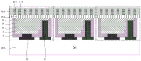
请参阅图1,本申请实施例提供一种发光二极管芯片,包括至少一个发光二极管。发光二极管包括:外延结构1。外延结构1包括:层叠设置的N型半导体叠层、发光层14和P型半导体层15。Referring to FIG. 1 , an embodiment of the present application provides a light emitting diode chip, including at least one light emitting diode. The light emitting diode includes: an epitaxial structure 1 . The epitaxial structure 1 includes: an N-type semiconductor stack, a
N型半导体叠层包括:层叠设置的第一层N型半导体层11、本征半导体层12和第二层N型半导体层13。其中,第一层N型半导体层11位于第二层N型半导体层13背离发光层14的一侧。第一层N型半导体层11包括:具有若干孔洞H的N型半导体基底110,以及填充于孔洞H内的若干散射微粒112。The N-type semiconductor stack includes: a first N-
此处,外延结构1可以采用磊晶工艺外延生长于生长衬底上。生长衬底例如为蓝宝石衬底或氮化镓衬底,但并不仅限于此。Here, the epitaxial structure 1 can be epitaxially grown on the growth substrate by using an epitaxial process. The growth substrate is, for example, a sapphire substrate or a gallium nitride substrate, but not limited thereto.
可选的,第一层N型半导体层11和第二层N型半导体层13为N型氮化镓层。本征半导体层12为本征氮化镓层。发光层14为多量子阱(Multiple Quantum Well,简称MQW)。P型半导体层15为P型氮化镓层。Optionally, the first N-
本申请实施例中,第一层N型半导体层11位于第二层N型半导体层13背离发光层14的一侧,可以使得发光二极管从N型半导体叠层一侧传输的光波在穿过第一层N型半导体层11后再出射。由于第一层N型半导体层11中具有若干孔洞H、以及填充于孔洞H内的若干散射微粒112,因此可以利用多个散射微粒112对光波进行散射,从而有效提升单个发光二极管的出光均匀性和出光效率。In the embodiment of the present application, the first N-
基于此,本申请实施例在发光层14的出光侧设置N型半导体叠层,可以利用第二层N型半导体层13向发光层14提供载流子,以满足发光层14发光的需求;并且,利用第一层N型半导体层11对发光层14出射的光波进行匀光处理,以提升单个发光二极管的出光均匀性和出光效率。同时,本征半导体层12位于第一层N型半导体层11和第二层N型半导体层13之间,可以有效隔离第一层N型半导体层11和第二层N型半导体层13。Based on this, in the embodiment of the present application, an N-type semiconductor stack is arranged on the light-emitting side of the light-emitting
此外,N型半导体叠层中的第一层N型半导体层11和第二层N型半导体层13,可以采用相同的本征半导体材料分别进行掺杂来获得,从而有利于简化发光二极管芯片的制备工艺,以提高生产效率。In addition, the first N-
请参阅图1和图2,在一些实施例中,第一层N型半导体层11中的若干孔洞H均匀分布,且各孔洞H的轴线垂直于N型半导体基底110。这样不仅方便于制备,也有利于进一步提升第一层N型半导体层11的匀光效果。Referring to FIG. 1 and FIG. 2 , in some embodiments, the holes H in the first N-
此处,孔洞H的形状和尺寸,可以根据实际需求选择设置。Here, the shape and size of the hole H can be selected and set according to actual needs.
可选的,请参阅图1,沿第一层N型半导体层11的厚度方向,孔洞H贯穿N型半导体基底110。也即,沿第一层N型半导体层11的厚度方向,孔洞H的深度等于N型半导体基底110厚度。如此,有利于在孔洞H内填充较多的散射微粒112。Optionally, please refer to FIG. 1 , along the thickness direction of the first N-
孔洞H的深度并不仅限于此。例如,请参阅图2,沿第一层N型半导体层11的厚度方向,孔洞H的深度小于N型半导体基底110厚度。The depth of the hole H is not limited to this. For example, referring to FIG. 2 , along the thickness direction of the first N-
此外,上述实施例中,散射微粒112用于对光波进行散射,散射微粒112为纳米级微粒,散射微粒112可以选用具有良好光学性能的材料制备获得,以确保其具有良好的匀光效果。示例的,散射微粒112为氧化物微粒,例如为氧化硅微粒、氧化锌微粒或氧化铝微粒中的至少一种。In addition, in the above embodiments, the scattering
可以理解的是,在一些实施例中,如图1和图2中所示,第一层N型半导体层11的孔洞H内可以仅填充有散射微粒112。例如,本申请实施例可以将若干散射微粒112混合至有机溶剂中,并将混合有散射微粒112的有机溶剂注入孔洞H内,然后去除有机溶剂,仅保留散射微粒112于孔洞H内。有机溶剂例如为甲醇、乙醇、丙酮、甲苯或己烷,如此便于通过蒸发或挥发的方式去除。It can be understood that, in some embodiments, as shown in FIG. 1 and FIG. 2 , the holes H in the first N-
此外,在另一些实施例中,请参阅图3,第一层N型半导体层11还包括微粒载体113。微粒载体113填充于孔洞H内,且散射微粒112掺杂于微粒载体113内。In addition, in some other embodiments, referring to FIG. 3 , the first N-
此处,可选的,微粒载体113为环氧树脂或透明硅胶。Here, optionally, the
如此,本申请实施例可以先将散射微粒112掺杂于微粒载体113内,再将该微粒载体113旋涂注入孔洞H内,以简化第一层N型半导体层11的制备工艺。In this way, in the embodiment of the present application, the scattering
需要补充的是,在发光二极管中,P型半导体层15、发光层14和第二层N型半导体层13通常图形化为台面结构(MESA)。例如,第二层N型半导体层13的背离本征半导体层12的表面呈台阶状。发光层14部分覆盖第二层N型半导体层13,即覆盖第二层N型半导体层13的上台阶面。P型半导体层15覆盖发光层14,且P型半导体层15和发光层14在第二层N型半导体层13上的正投影重叠。What needs to be added is that in light emitting diodes, the P-
请参阅图1~图3,发光二极管还包括:第一反射电极31和第二反射电极32。第一反射电极31位于第二层N型半导体层13的背离本征半导体层12的一侧,且与第二层N型半导体层13连接。第二反射电极32位于P型半导体层15的背离发光层14的一侧,且与P型半导体层15连接。Referring to FIGS. 1-3 , the light emitting diode further includes: a first
此处,第一反射电极31和第二反射电极32位于P型半导体层15所在的一侧,可以对发光层14出射向P型半导体层15的光波进行反射,以提高发光二极管的出光效率。Here, the first
可选的,第一反射电极31和第二反射电极32采用具有良好导电率和良好光反射率的金属制成,例如银、金、铟或锡等。Optionally, the first
可以理解的是,请继续参阅图1~图3,发光二极管还包括:电流扩展层2。电流扩展层2位于P型半导体层15和第二反射电极32之间,且分别连接P型半导体层15和第二反射电极32。也即,第二反射电极32通过电流扩展层2与P型半导体层15连接。It can be understood that, please continue to refer to FIG. 1 to FIG. 3 , the light emitting diode further includes: a current spreading
可选的,电流扩展层2采用可见光透过率高且导电能力强的透明导电材料制备形成。透明导电材料例如为氧化铟锡(ITO)、氧化锌(ZnO)、氧化镉锡(CTO)、氧化铟(InO)、铟(In)掺杂氧化锌(ZnO)、铝(Al)掺杂氧化锌(ZnO)、或镓(Ga)掺杂氧化锌(ZnO)等。Optionally, the current spreading
在一个示例中,电流扩展层2为ITO层。电流扩展层2具有较高的导电率以及较高的可见光透过率,能够有效提高发光层14的出光效率。In one example, the current spreading
需要补充的是,请继续参阅图1~图3,发光二极管还包括:绝缘层4。绝缘层4覆盖电流扩展层2、P型半导体层15、发光层14及第二层N型半导体层13的裸露表面,且具有第一开口K1和第二开口K2。其中,第一开口K1暴露出第二层N型半导体层13的部分表面,第一反射电极31位于第一开口K1内并与第二层N型半导体层13连接。第二开口K2暴露出电流扩展层2的部分表面,第二反射电极32位于第二开口K2内并与电流扩展层2连接。What needs to be added is that please continue to refer to FIG. 1 to FIG. 3 , the light emitting diode further includes: an insulating
此处,绝缘层4可以为单层结构或叠层结构。Here, the insulating
在一个示例中,绝缘层4包括:沿远离电流扩展层2的方向依次设置的分布式布拉格反射镜(Distributed Bragg Reflection,简称DBR)和钝化层。钝化层例如为氧化硅层或氮化硅层。如此可以利用DBR有效提升发光二极管的出光效率,并利用钝化层绝缘保护发光二极管。In one example, the insulating
本申请实施例提供的发光二极管芯片在进行出光效果的测试之后,例如采用对光波变化敏感的光敏材料,以使发光二极管芯片出射的光波照射至该光敏材料上,这样光敏材料中被大能量光波照射的区域会有相对应的损失。在针对多个相同尺寸的发光二极管芯片进行同等电流点亮的测试之后,传统的发光二极管芯片对应的光敏材料容易出现两个比较明显的暗点,然而本申请实施例提供的发光二极管芯片对应的光敏材料整体变化均匀,证明本申请实施例提供的单个发光二极管芯片具有优良的出光均匀性及出光效率。根据测试效果,相较于相同尺寸的传统发光二极管芯片,本申请实施例提供的单个发光二极管芯片的出光强度可以增大3%~9%。After the light-emitting diode chip provided in the embodiment of the application is tested for its light-extracting effect, for example, a photosensitive material sensitive to light wave changes is used, so that the light wave emitted by the light-emitting diode chip irradiates the photosensitive material, so that the light wave emitted by the light-emitting diode chip is irradiated on the photosensitive material. There will be a corresponding loss in the irradiated area. After performing the same current lighting test on multiple LED chips of the same size, the photosensitive material corresponding to the traditional LED chip is prone to two relatively obvious dark spots, but the LED chip provided by the embodiment of the application corresponds to The overall change of the photosensitive material is uniform, which proves that the single light-emitting diode chip provided by the embodiment of the present application has excellent light-emitting uniformity and light-emitting efficiency. According to test results, compared with conventional light emitting diode chips of the same size, the light output intensity of a single light emitting diode chip provided in the embodiment of the present application can be increased by 3% to 9%.
基于同样的发明构思,本申请实施例还提供一种发光二极管芯片的制备方法,用于制备上述一些实施例中的发光二极管。Based on the same inventive concept, the embodiments of the present application also provide a method for manufacturing a light emitting diode chip, which is used to prepare the light emitting diodes in some of the above embodiments.
请参阅图4,发光二极管芯片的制备方法包括以下步骤。Please refer to FIG. 4 , the manufacturing method of the LED chip includes the following steps.
S100,提供生长衬底,在生长衬底上生长外延材料层。S100, providing a growth substrate, and growing an epitaxial material layer on the growth substrate.
外延材料层包括:沿远离生长衬底的方向依次生长的第一层本征半导体材料层、第一层N型半导体材料层、第二层本征半导体材料层、第二层N型半导体材料层、发光材料层和P型半导体材料层。The epitaxial material layer includes: the first intrinsic semiconductor material layer, the first N-type semiconductor material layer, the second intrinsic semiconductor material layer, and the second N-type semiconductor material layer grown sequentially along the direction away from the growth substrate. , a luminescent material layer and a P-type semiconductor material layer.
此处,生长衬底例如为蓝宝石衬底或氮化镓衬底,但并不仅限于此。Here, the growth substrate is, for example, a sapphire substrate or a gallium nitride substrate, but is not limited thereto.
可选的,第一层N型半导体材料层和第二层N型半导体材料层为N型氮化镓材料层。本征半导体材料层为本征氮化镓材料层。发光材料层为多量子阱(Multiple QuantumWell,简称MQW)材料层。P型半导体材料层为P型氮化镓材料层。Optionally, the first N-type semiconductor material layer and the second N-type semiconductor material layer are N-type gallium nitride material layers. The intrinsic semiconductor material layer is an intrinsic gallium nitride material layer. The luminescent material layer is a multiple quantum well (Multiple Quantum Well, MQW for short) material layer. The P-type semiconductor material layer is a P-type gallium nitride material layer.
S200,将第二层N型半导体材料层、发光材料层和P型半导体材料层图形化,形成第二层N型半导体层、发光层和P型半导体层。S200, patterning the second N-type semiconductor material layer, light-emitting material layer and P-type semiconductor material layer to form the second N-type semiconductor layer, light-emitting layer and P-type semiconductor layer.
此处,第二层N型半导体层、发光层和P型半导体层构成发光二极管的台面结构。Here, the second N-type semiconductor layer, the light-emitting layer and the P-type semiconductor layer constitute the mesa structure of the light-emitting diode.
S300,将P型半导体层、发光层、第二层N型半导体层、第二层本征半导体材料层、第一层N型半导体材料层、以及第一层本征半导体材料层,从生长衬底上转移至转移衬底上。S300, forming the P-type semiconductor layer, the light emitting layer, the second N-type semiconductor layer, the second intrinsic semiconductor material layer, the first N-type semiconductor material layer, and the first intrinsic semiconductor material layer from the growth substrate transferred onto the transfer substrate.
此处,转移衬底可以为临时衬底,也可以为永久衬底。Here, the transfer substrate can be either a temporary substrate or a permanent substrate.
S400,去除第一层本征半导体材料层,并抛光第一层N型半导体材料层。S400, removing the first intrinsic semiconductor material layer, and polishing the first N-type semiconductor material layer.
S500,在抛光后的第一层N型半导体材料层中形成若干孔洞。S500, forming several holes in the polished first N-type semiconductor material layer.
可选的,若干孔洞采用电化学刻蚀工艺形成。Optionally, several holes are formed by electrochemical etching process.
可选的,若干孔洞均匀分布,且各孔洞的轴线垂直于抛光后的第一层N型半导体材料层。Optionally, the holes are evenly distributed, and the axis of each hole is perpendicular to the polished first N-type semiconductor material layer.
此外,孔洞的形状和尺寸,可以根据实际需求选择设置。In addition, the shape and size of the hole can be selected and set according to actual needs.
可选的,沿抛光后的第一层N型半导体材料层的厚度方向,孔洞的深度小于或等于抛光后的第一层N型半导体材料层的厚度。Optionally, along the thickness direction of the polished first N-type semiconductor material layer, the depth of the holes is less than or equal to the thickness of the polished first N-type semiconductor material layer.
S600,在孔洞内填充若干散射微粒。S600, filling the hole with some scattering particles.
可选的,在孔洞内填充若干散射微粒,具体有以下三种实施方式。Optionally, a number of scattering particles are filled in the hole, specifically, there are the following three implementation manners.
第一种实施方式,将若干散射微粒混合至有机溶剂中,并将混合有散射微粒的有机溶剂注入孔洞内,然后去除有机溶剂。In the first embodiment, a number of scattering particles are mixed into an organic solvent, and the organic solvent mixed with the scattering particles is injected into the holes, and then the organic solvent is removed.
此处,有机溶剂例如为甲醇、乙醇、丙酮、甲苯或己烷,以便于通过蒸发或挥发的方式去除。如此,抛光后的第一层N型半导体材料层的孔洞内仅填充有散射微粒。Here, the organic solvent is, for example, methanol, ethanol, acetone, toluene or hexane, so as to be removed by evaporation or volatilization. In this way, the holes in the polished first N-type semiconductor material layer are only filled with scattering particles.
第二种实施方式,将若干散射微粒混合至环氧树脂中,并将混合有散射微粒的环氧树脂旋涂注入孔洞内,然后固化环氧树脂。In the second embodiment, a number of scattering particles are mixed into the epoxy resin, and the epoxy resin mixed with the scattering particles is spin-coated and injected into the holes, and then the epoxy resin is cured.
第三种实施方式,将若干散射微粒混合至透明硅胶中,并将混合有散射微粒的透明硅胶旋涂注入孔洞内,然后固化透明硅胶。In the third embodiment, a number of scattering particles are mixed into the transparent silica gel, and the transparent silica gel mixed with the scattering particles is spin-coated and injected into the holes, and then the transparent silica gel is cured.
通过第二种实施方式或第三种实施方式制备的所得结构中,抛光后的第一层N型半导体材料层的孔洞内还填充有微粒载体,散射微粒掺杂于微粒载体中。In the obtained structure prepared through the second embodiment or the third embodiment, the pores of the polished first N-type semiconductor material layer are also filled with particle carriers, and the scattering particles are doped in the particle carriers.
此外,散射微粒用于对光波进行散射,散射微粒为纳米级微粒,散射微粒可以选用具有良好光学性能的材料制备获得,以确保其具有良好的匀光效果。可选的,散射微粒为氧化物微粒,例如为氧化硅微粒、氧化锌微粒或氧化铝微粒中的至少一种。In addition, the scattering particles are used to scatter light waves, and the scattering particles are nanoscale particles. The scattering particles can be prepared from materials with good optical properties to ensure that they have a good uniform light effect. Optionally, the scattering particles are oxide particles, such as at least one of silicon oxide particles, zinc oxide particles or aluminum oxide particles.
S700,将第二层本征半导体材料层、以及填充散射微粒后的第一层N型半导体材料层图形化,形成本征半导体层和第一层N型半导体层。S700, patterning the second intrinsic semiconductor material layer and the first N-type semiconductor material layer filled with scattering particles to form an intrinsic semiconductor layer and a first N-type semiconductor layer.
上述发光二极管芯片的制备方法,用于制备前述一些实施例中的发光二极管芯片。前述发光二极管芯片所能实现的技术效果,该制备方法也均能实现,此处不再详述。The above method for preparing the light emitting diode chip is used to prepare the light emitting diode chip in some of the aforementioned embodiments. The technical effects that can be achieved by the foregoing light-emitting diode chip can also be achieved by this preparation method, and will not be described in detail here.
在一些实施例中,请参阅图5,在执行S300之前,发光二极管的制备方法还包括如下步骤。In some embodiments, referring to FIG. 5 , before performing S300 , the manufacturing method of the light emitting diode further includes the following steps.
S220,在第二层N型半导体层的背离第二层本征半导体材料层的一侧形成第一反射电极,在P型半导体层的背离发光层的一侧形成第二反射电极,以使第一反射电极与第二层N型半导体层连接,第二反射电极与P型半导体层连接。S220, forming a first reflective electrode on the side of the second N-type semiconductor layer away from the second intrinsic semiconductor material layer, and forming a second reflective electrode on the side of the P-type semiconductor layer away from the light-emitting layer, so that the first A reflective electrode is connected with the second N-type semiconductor layer, and the second reflective electrode is connected with the P-type semiconductor layer.
此处,第一反射电极和第二反射电极位于P型半导体层所在的一侧,可以对发光层出射向P型半导体层的光波进行反射,以提高发光二极管的出光效率。Here, the first reflective electrode and the second reflective electrode are located on the side where the P-type semiconductor layer is located, and can reflect light waves emitted from the light-emitting layer to the P-type semiconductor layer, so as to improve the light extraction efficiency of the light-emitting diode.
可选的,第一反射电极和第二反射电极采用具有良好导电率和良好光反射率的金属制成,例如银、金、铟或锡等。Optionally, the first reflective electrode and the second reflective electrode are made of metal with good electrical conductivity and good light reflectivity, such as silver, gold, indium or tin.
相应的,步骤S300包括如下步骤。Correspondingly, step S300 includes the following steps.
S301,将第一反射电极和第二反射电极键合至转移衬底上。S301, bonding the first reflective electrode and the second reflective electrode to the transfer substrate.
此处,转移衬底例如为永久衬底。Here, the transfer substrate is, for example, a permanent substrate.
在一个示例中,转移衬底为发光二极管的驱动背板。转移衬底上设置有用于与第一反射电极对应键合的第一驱动电极,以及与第二反射电极对应键合的第二驱动电极。In one example, the transfer substrate is a drive backplane for light emitting diodes. The transfer substrate is provided with a first driving electrode for corresponding bonding with the first reflective electrode, and a second driving electrode for corresponding bonding with the second reflective electrode.
按照反射电极和驱动电极的材料,第一反射电极与第一驱动电极的键合,以及第二反射电极与第二驱动电极的键合,可以为银-铟键合、银-锡键合、金-金键合、铟-铟键合、金-银键合或铟-锡键合中的一种。According to the materials of the reflective electrode and the driving electrode, the bonding of the first reflective electrode and the first driving electrode, and the bonding of the second reflective electrode and the second driving electrode can be silver-indium bonding, silver-tin bonding, One of gold-gold bonding, indium-indium bonding, gold-silver bonding, or indium-tin bonding.
S302,剥离生长衬底。S302, peeling off the growth substrate.
此处,生长衬底可以采用激光剥离工艺剥离。Here, the growth substrate can be lifted off using a laser lift-off process.
需要补充的是,在一些示例中,在执行步骤S200之前,发光二极管芯片的制备方法还包括如下步骤。What needs to be added is that, in some examples, before step S200 is performed, the method for manufacturing a light emitting diode chip further includes the following steps.
S110,形成覆盖P型半导体层材料层的电流扩展材料层。S110, forming a current spreading material layer covering the material layer of the P-type semiconductor layer.
此处,电流扩展材料层为透明导电材料层。透明导电材料层的材料例如为氧化铟锡(ITO)、氧化锌(ZnO)、氧化镉锡(CTO)、氧化铟(InO)、铟(In)掺杂氧化锌(ZnO)、铝(Al)掺杂氧化锌(ZnO)、或镓(Ga)掺杂氧化锌(ZnO)等。Here, the current spreading material layer is a transparent conductive material layer. The material of the transparent conductive material layer is, for example, indium tin oxide (ITO), zinc oxide (ZnO), cadmium tin oxide (CTO), indium oxide (InO), indium (In) doped zinc oxide (ZnO), aluminum (Al) Doped zinc oxide (ZnO), or gallium (Ga) doped zinc oxide (ZnO), etc.
相应的,S200还包括:将电流扩展材料层图形化,形成电流扩展层。Correspondingly, S200 further includes: patterning the current spreading material layer to form a current spreading layer.
在一些示例中,在执行步骤S220之前,发光二极管芯片的制备方法还包括如下步骤。In some examples, before step S220 is performed, the manufacturing method of the light emitting diode chip further includes the following steps.
S210,形成覆盖电流扩展层、P型半导体层、发光层及第二层N型半导体层的裸露表面的绝缘材料层,并将绝缘材料层图形化,形成具有第一开口和第二开口的绝缘层。其中,第一开口暴露出第二层N型半导体层的部分表面,第二开口暴露出电流扩展层的部分表面。S210, forming an insulating material layer covering the exposed surfaces of the current spreading layer, the P-type semiconductor layer, the light-emitting layer, and the second N-type semiconductor layer, and patterning the insulating material layer to form an insulating layer having a first opening and a second opening. layer. Wherein, the first opening exposes a part of the surface of the second N-type semiconductor layer, and the second opening exposes a part of the surface of the current spreading layer.
此处,绝缘层可以为单层结构或叠层结构。Here, the insulating layer may have a single-layer structure or a stacked-layer structure.
相应的,步骤S220包括,在第一开口内形成第一反射电极,在第二开口内形成第二反射电极,以使第一反射电极与第二层N型半导体层连接,第二反射电极与电流扩展层连接。Correspondingly, step S220 includes forming a first reflective electrode in the first opening, forming a second reflective electrode in the second opening, so that the first reflective electrode is connected to the second N-type semiconductor layer, and the second reflective electrode is connected to the second N-type semiconductor layer. Current spreading layer connection.
为了更清楚的说明本申请实施例中发光二极管芯片的制备方法,以下以图3中所示的发光二极管芯片为例进行详述。In order to more clearly illustrate the method for preparing the light emitting diode chip in the embodiment of the present application, the light emitting diode chip shown in FIG. 3 is taken as an example to describe in detail below.
S100,如图6中所示,提供生长衬底101,在生长衬底101上生长外延材料层10。外延材料层10包括:沿远离生长衬底101的方向依次生长的第一层本征半导体材料层010、第一层N型半导体材料层011、第二层本征半导体材料层012、第二层N型半导体材料层013、发光材料层014和P型半导体材料层015。S100 , as shown in FIG. 6 , a
此处,生长衬底101为蓝宝石衬底。外延材料层10采用磊晶工艺生产形成。其中,第一层N型半导体材料层011和第二层N型半导体材料层013为N型氮化镓材料层,N型氮化镓材料层的掺杂浓度大于或等于4E18/cm3。第一层本征半导体材料层010和第二层本征半导体材料层012为本征氮化镓材料层。发光材料层014为多量子阱(Multiple Quantum Well,简称MQW)材料层。P型半导体材料层015为P型氮化镓材料层。Here, the
S110,如图7中所示,形成覆盖P型半导体层材料层015的电流扩展材料层20。S110 , as shown in FIG. 7 , forming a current spreading
此处,电流扩展材料层20为ITO材料层。Here, the current spreading
S200,如图8中所示,将第二层N型半导体材料层013、发光材料层014、P型半导体材料层015和电流扩展材料层20图形化,形成第二层N型半导体层13、发光层14、P型半导体层15和电流扩展层2。S200, as shown in FIG. 8 , pattern the second N-type semiconductor material layer 013, the
此处,图形化工艺可以采用电感耦合等离子体(Inductively Couple PlasmaEtch,简称ICP)刻蚀实现。P型半导体层15、发光层14和第二层N型半导体层13构成台面结构(MESA)。电流扩展层2部分覆盖P型半导体层15。Here, the patterning process can be implemented by using Inductively Coupled Plasma (Inductively Coupled PlasmaEtch, ICP for short) etching. The P-
S210,如图9中所示,形成覆盖电流扩展层2、P型半导体层15、发光层14及第二层N型半导体层13的裸露表面的绝缘材料层,并将绝缘材料层图形化,形成具有第一开口K1和第二开口K2的绝缘层4。其中,第一开口K1暴露出第二层N型半导体层13的部分表面,第二开口K2暴露出电流扩展层2的部分表面。S210, as shown in FIG. 9, forming an insulating material layer covering the exposed surfaces of the current spreading
可选的,绝缘层4包括:沿远离电流扩展层2的方向依次设置的分布式布拉格反射镜(Distributed Bragg Reflection,简称DBR)和钝化层。钝化层例如为氧化硅层或氮化硅层。Optionally, the insulating
S220,如图10中所示,在第一开口K1内形成第一反射电极31,在第二开口K2内形成第二反射电极32,以使第一反射电极31与第二层N型半导体层13连接,第二反射电极32与电流扩展层2连接。S220, as shown in FIG. 10, form the first
S301,如图11中所示,将第一反射电极31和第二反射电极32键合至转移衬底102上,以将绝缘层4、电流扩展层2、P型半导体层15、发光层14、第二层N型半导体层13、第二层本征半导体材料层012、第一层N型半导体材料层011、第一层本征半导体材料层010以及生长衬底101转移至转移衬底102上。S301, as shown in FIG. 11 , bonding the first
此处,转移衬底102为发光二极管的驱动背板。转移衬底102上设置有用于与第一反射电极31对应键合的第一驱动电极,以及与第二反射电极32对应键合的第二驱动电极。Here, the
按照反射电极和驱动电极的材料,第一反射电极31与第一驱动电极的键合,以及第二反射电极32与第二驱动电极的键合,可以为银-铟键合、银-锡键合、金-金键合、铟-铟键合、金-银键合或铟-锡键合中的一种。According to the materials of the reflective electrode and the driving electrode, the bonding of the first
S302,如图12中所示,剥离生长衬底101。S302, as shown in FIG. 12 , peel off the
此处,生长衬底101采用激光剥离工艺剥离,例如准分子激光面剥离工艺,可以具有较高的剥离良率。可选的,激光波长为194nm;个剥离面的最大面积为500μm×500μm。Here, the
S400,如图13中所示,去除第一层本征半导体材料层010,并抛光第一层N型半导体材料层011。S400, as shown in FIG. 13 , removing the first intrinsic
此处,第一层本征半导体材料层010可以通过干法刻蚀去除,例如采用ICP刻蚀设备完成。并且,第一层N型半导体材料层011的抛光,也可以通过第一层本征半导体材料层010的去除工艺同步实现。也即,刻蚀去除厚度大于第一层本征半导体材料层010的材料。Here, the first intrinsic
S500,如图14中所示,在抛光后的第一层N型半导体材料层011中形成若干孔洞H。S500, as shown in FIG. 14 , forming several holes H in the polished first N-type
此处,孔洞H为纳米级孔洞,可以采用电化学刻蚀工艺形成。Here, the hole H is a nanoscale hole, which can be formed by an electrochemical etching process.
可选的,形成孔洞H的电化学刻蚀溶液为醋酸、盐酸或草酸等酸性溶液中的至少一种。Optionally, the electrochemical etching solution for forming the holes H is at least one of acidic solutions such as acetic acid, hydrochloric acid or oxalic acid.
可选的,形成孔洞H的电化学刻蚀所需的电压范围为10V~40V,例如为10V、15V、20V、25V、30V、35V或40V。Optionally, the voltage range required for the electrochemical etching to form the hole H is 10V-40V, such as 10V, 15V, 20V, 25V, 30V, 35V or 40V.
可选的,孔洞H为柱形孔,孔洞H的孔径的取值范围为:200埃~5000埃。孔洞H的深度的取值范围为:20000埃~40000埃。Optionally, the hole H is a cylindrical hole, and the value range of the pore diameter of the hole H is: 200 angstroms to 5000 angstroms. The depth of the hole H ranges from 20000 angstroms to 40000 angstroms.
S600,如图15中所示,在孔洞H内填充若干散射微粒112。S600, as shown in FIG. 15 , fill the hole H with a number of scattering
可选的,将若干散射微粒112混合至微粒载体(透明硅胶)113中,并采用匀胶工艺将混合有散射微粒112的微粒载体113旋涂注入孔洞H内,然后固化微粒载体113。Optionally, a number of scattering
S700,如图16中所示,将第二层本征半导体材料层012、以及填充散射微粒112后的第一层N型半导体材料层011图形化,形成本征半导体层12和第一层N型半导体层11。S700, as shown in FIG. 16 , pattern the second intrinsic
需要补充的是,在执行步骤S700之后,可以根据实际需求对所得结构进行芯片后端工艺,例如切割,以获得多个独立的发光二极管芯片。It should be added that, after step S700 is performed, chip back-end processes, such as dicing, may be performed on the obtained structure according to actual needs, so as to obtain multiple independent light-emitting diode chips.
基于同样的发明构思,本申请实施例还提供一种显示装置,包括:驱动电路,以及与驱动电路连接的发光单元。其中,发光单元包括如上一些实施例中所述的发光二极管芯片。Based on the same inventive concept, an embodiment of the present application further provides a display device, including: a driving circuit, and a light emitting unit connected to the driving circuit. Wherein, the light emitting unit includes the light emitting diode chip as described in some embodiments above.
可选的,显示装置为发光二极管显示面板或发光二极管背板。Optionally, the display device is a light emitting diode display panel or a light emitting diode backplane.
前述发光二极管芯片所能实现的技术效果,本申请实施例中的显示装置也均能实现,此处不再详述。The technical effects that can be achieved by the aforementioned light emitting diode chips can also be achieved by the display device in the embodiment of the present application, and will not be described in detail here.
应当理解的是,本发明的应用不限于上述的举例,对本领域普通技术人员来说,可以根据上述说明加以改进或变换,所有这些改进和变换都应属于本发明所附权利要求的保护范围。It should be understood that the application of the present invention is not limited to the above examples, and those skilled in the art can make improvements or transformations according to the above descriptions, and all these improvements and transformations should belong to the protection scope of the appended claims of the present invention.
Claims (10)
Priority Applications (1)
| Application Number | Priority Date | Filing Date | Title |
|---|---|---|---|
| CN202111315519.5A CN114050210B (en) | 2021-11-08 | 2021-11-08 | Light-emitting diode chip, manufacturing method thereof, and display device |
Applications Claiming Priority (1)
| Application Number | Priority Date | Filing Date | Title |
|---|---|---|---|
| CN202111315519.5A CN114050210B (en) | 2021-11-08 | 2021-11-08 | Light-emitting diode chip, manufacturing method thereof, and display device |
Publications (2)
| Publication Number | Publication Date |
|---|---|
| CN114050210A CN114050210A (en) | 2022-02-15 |
| CN114050210B true CN114050210B (en) | 2023-04-14 |
Family
ID=80207772
Family Applications (1)
| Application Number | Title | Priority Date | Filing Date |
|---|---|---|---|
| CN202111315519.5A Active CN114050210B (en) | 2021-11-08 | 2021-11-08 | Light-emitting diode chip, manufacturing method thereof, and display device |
Country Status (1)
| Country | Link |
|---|---|
| CN (1) | CN114050210B (en) |
Families Citing this family (4)
| Publication number | Priority date | Publication date | Assignee | Title |
|---|---|---|---|---|
| CN114551693A (en) * | 2022-02-21 | 2022-05-27 | 东莞市中麒光电技术有限公司 | High-efficiency filling method of quantum dots, light-color conversion structure and light-emitting chip |
| CN114664997A (en) * | 2022-03-14 | 2022-06-24 | Tcl华星光电技术有限公司 | Light emitting diode, light emitting substrate and display device |
| CN115332404B (en) * | 2022-08-04 | 2024-11-08 | 中国科学院上海微系统与信息技术研究所 | Preparation method of hybrid integrated quantum light source LED device |
| CN116682912B (en) * | 2023-06-21 | 2024-05-28 | 惠科股份有限公司 | Light emitting chip, display panel, light emitting assembly and manufacturing method thereof |
Citations (3)
| Publication number | Priority date | Publication date | Assignee | Title |
|---|---|---|---|---|
| CN101459209A (en) * | 2007-12-14 | 2009-06-17 | 台达电子工业股份有限公司 | Light emitting diode device and manufacturing method thereof |
| CN104051587A (en) * | 2014-06-19 | 2014-09-17 | 中国科学院半导体研究所 | Preparation method of surface plasmon-enhanced GaN-based nanohole LED |
| WO2016208993A1 (en) * | 2015-06-23 | 2016-12-29 | 엘지이노텍 주식회사 | Light-emitting element and display device comprising same |
Family Cites Families (3)
| Publication number | Priority date | Publication date | Assignee | Title |
|---|---|---|---|---|
| GB0722054D0 (en) * | 2007-11-09 | 2007-12-19 | Photonstar Led Ltd | LED with enhanced light extraction |
| TWI370560B (en) * | 2007-12-14 | 2012-08-11 | Delta Electronics Inc | Light-emitting diode device and manufacturing method thereof |
| US11189757B2 (en) * | 2019-12-12 | 2021-11-30 | Lumileds Llc | Light emitting diodes with reflective sidewalls comprising porous particles |
-
2021
- 2021-11-08 CN CN202111315519.5A patent/CN114050210B/en active Active
Patent Citations (3)
| Publication number | Priority date | Publication date | Assignee | Title |
|---|---|---|---|---|
| CN101459209A (en) * | 2007-12-14 | 2009-06-17 | 台达电子工业股份有限公司 | Light emitting diode device and manufacturing method thereof |
| CN104051587A (en) * | 2014-06-19 | 2014-09-17 | 中国科学院半导体研究所 | Preparation method of surface plasmon-enhanced GaN-based nanohole LED |
| WO2016208993A1 (en) * | 2015-06-23 | 2016-12-29 | 엘지이노텍 주식회사 | Light-emitting element and display device comprising same |
Also Published As
| Publication number | Publication date |
|---|---|
| CN114050210A (en) | 2022-02-15 |
Similar Documents
| Publication | Publication Date | Title |
|---|---|---|
| CN114050210B (en) | Light-emitting diode chip, manufacturing method thereof, and display device | |
| JP7484727B2 (en) | Light emitting device and image display device | |
| US20250275341A1 (en) | Micro led micro-display chip and manufacturing method thereof | |
| CN107210315B (en) | Integrated color LED micro-display | |
| CN101449398B (en) | Light emitting element | |
| US20150194586A1 (en) | Light-emitting device having a plurality of contact parts | |
| TWI495141B (en) | Wafer light emitting structure forming method and light source generating device | |
| CN109417082A (en) | Semiconductor devices and display device including semiconductor devices | |
| US20240258474A1 (en) | Led chip and method for manufacturing the same, and display device | |
| CN109075221A (en) | Luminescent device and display including luminescent device | |
| CN117276304A (en) | Micro light-emitting diode display device and preparation method thereof | |
| CN113169252A (en) | Light-emitting diode | |
| CN101958374B (en) | Light emitting element and manufacturing method thereof | |
| KR101014339B1 (en) | Nitride light emitting device having improved luminous efficiency and manufacturing method thereof | |
| CN113629095B (en) | Light emitting display device and method for manufacturing light emitting display device | |
| CN203607447U (en) | Led chip | |
| JP2024541078A (en) | Light emitting diode array having inactive implanted isolation regions and method of forming same - Patents.com | |
| CN109065689A (en) | A kind of Micro LED encapsulation structure and preparation method thereof | |
| CN110957409B (en) | Light emitting diode epitaxial wafer, light emitting diode module and manufacturing method thereof | |
| CN111613696B (en) | MICRO LED structure and manufacturing method thereof | |
| CN102064251B (en) | High-power SiC substrate vertical structure light-emitting diode and preparation method thereof | |
| KR100936058B1 (en) | Nitride light emitting device manufacturing method and nitride light emitting device with improved luminous efficiency using a gradient incident deposition method | |
| CN1812146A (en) | Highlight extract efficiency LED electrode and producing method thereof | |
| CN1649178A (en) | Light-emitting diode element, flip-chip light-emitting diode packaging structure and light reflection structure | |
| US20160218246A1 (en) | EPITAXIAL TRANSPARENT CONDUCTIVE OXIDE ELECTRODES FOR GaN LEDS |
Legal Events
| Date | Code | Title | Description |
|---|---|---|---|
| PB01 | Publication | ||
| PB01 | Publication | ||
| SE01 | Entry into force of request for substantive examination | ||
| SE01 | Entry into force of request for substantive examination | ||
| GR01 | Patent grant | ||
| GR01 | Patent grant | ||
| CP03 | Change of name, title or address | ||
| CP03 | Change of name, title or address |
Address after: 402760 No.69, Wushan Road, Biquan street, Bishan District, Chongqing Patentee after: Chongqing Kangjia Optoelectronic Technology Co.,Ltd. Country or region after: China Address before: 402760 No.69, Wushan Road, Biquan street, Bishan District, Chongqing Patentee before: Chongqing Kangjia Photoelectric Technology Research Institute Co.,Ltd. Country or region before: China |