CN113779742A - Modeling method and device for simplified model of thermal resistance network and chip junction temperature prediction method - Google Patents
Modeling method and device for simplified model of thermal resistance network and chip junction temperature prediction method Download PDFInfo
- Publication number
- CN113779742A CN113779742A CN202111317957.5A CN202111317957A CN113779742A CN 113779742 A CN113779742 A CN 113779742A CN 202111317957 A CN202111317957 A CN 202111317957A CN 113779742 A CN113779742 A CN 113779742A
- Authority
- CN
- China
- Prior art keywords
- thermal resistance
- chip
- model
- resistance network
- value
- Prior art date
- Legal status (The legal status is an assumption and is not a legal conclusion. Google has not performed a legal analysis and makes no representation as to the accuracy of the status listed.)
- Granted
Links
Images


Classifications
-
- G—PHYSICS
- G06—COMPUTING OR CALCULATING; COUNTING
- G06F—ELECTRIC DIGITAL DATA PROCESSING
- G06F30/00—Computer-aided design [CAD]
- G06F30/10—Geometric CAD
- G06F30/18—Network design, e.g. design based on topological or interconnect aspects of utility systems, piping, heating ventilation air conditioning [HVAC] or cabling
-
- G—PHYSICS
- G06—COMPUTING OR CALCULATING; COUNTING
- G06F—ELECTRIC DIGITAL DATA PROCESSING
- G06F30/00—Computer-aided design [CAD]
- G06F30/20—Design optimisation, verification or simulation
-
- G—PHYSICS
- G06—COMPUTING OR CALCULATING; COUNTING
- G06F—ELECTRIC DIGITAL DATA PROCESSING
- G06F2113/00—Details relating to the application field
- G06F2113/18—Chip packaging
-
- G—PHYSICS
- G06—COMPUTING OR CALCULATING; COUNTING
- G06F—ELECTRIC DIGITAL DATA PROCESSING
- G06F2119/00—Details relating to the type or aim of the analysis or the optimisation
- G06F2119/08—Thermal analysis or thermal optimisation
Landscapes
- Engineering & Computer Science (AREA)
- Physics & Mathematics (AREA)
- Theoretical Computer Science (AREA)
- General Physics & Mathematics (AREA)
- Geometry (AREA)
- Computer Hardware Design (AREA)
- General Engineering & Computer Science (AREA)
- Evolutionary Computation (AREA)
- Computational Mathematics (AREA)
- Pure & Applied Mathematics (AREA)
- Mathematical Optimization (AREA)
- Mathematical Analysis (AREA)
- Computer Networks & Wireless Communication (AREA)
- Investigating Or Analyzing Materials Using Thermal Means (AREA)
Abstract
The application relates to the technical field of thermal reliability, and discloses a thermal resistance network simplified model modeling method, a thermal resistance network simplified model modeling device and a chip junction temperature prediction method. The thermal resistance network simplified model established by the method can be close to the entity chip, and the thermal resistance network simplified model is led into a server device simulating the actual working environment for simulation, so that the high-precision prediction of the junction temperature of the chip can be realized.
Description
Technical Field
The application relates to the technical field of thermal reliability, in particular to a thermal resistance network simplified model modeling method and device and a chip junction temperature prediction method.
Background
The increase of the power consumption of the chip causes the junction temperature of the chip to rise continuously, and the chip can fail due to overheating, so that the prediction of the junction temperature of the chip becomes more and more important.
In order to facilitate the calculation of the junction temperature of the chip under the actual working environment by the technicians, the currently commonly adopted method is as follows: and establishing a thermal resistance network simplified model of the chip, and introducing the thermal resistance network simplified model into a server device simulating an actual working environment for simulation, so as to obtain the junction temperature of the chip in the server device.
When the thermal resistance network simplified model of the chip is established, the thermal resistance network simplified model is generally established through thermal resistance parameters in a data manual, the model cannot be close to an entity chip, and the accuracy of predicting the junction temperature of the chip is not high.
Disclosure of Invention
Therefore, an object of the embodiments of the present application is to provide a modeling method and an apparatus for a simplified model of a thermal resistance network, and a method for predicting chip junction temperature, where the established simplified model of the thermal resistance network can be close to a physical chip, and the simplified model of the thermal resistance network is introduced into a server apparatus simulating an actual working environment for simulation, so as to realize high-precision prediction of the chip junction temperature.
In order to achieve the purpose, the technical scheme is as follows:
the first aspect of the present application provides a modeling method for a simplified model of a thermal resistance network, where the method includes:
selecting a plurality of surface nodes from a detailed model of a chip, and setting a network topological structure of a thermal resistance network simplified model according to the surface nodes;
setting a plurality of boundary conditions according to the application environment requirements of the chip, and calculating the chip thermal parameter values of the detailed model under each boundary condition, wherein the chip thermal parameter values comprise chip nodes and heat flows passing through each surface node;
constructing an objective function according to the thermal resistance network simplified model and the detailed model under each chip thermal parameter value under the boundary condition;
taking the value of the target function as an optimization parameter, taking each thermal resistance value of the thermal resistance network simplified model as a quantity to be solved, obtaining a thermal resistance combination which enables the value of the target function to be minimum through optimization calculation, taking the thermal resistance combination as the value of the quantity to be solved, and establishing the thermal resistance network simplified model according to the thermal resistance combination;
and carrying out simulation comparison verification on the established thermal resistance network simplified model and the detailed model under a preset boundary condition, and outputting the established thermal resistance network simplified model when the difference value of the simulated junction temperatures output by the thermal resistance network simplified model and the detailed model does not exceed a preset temperature difference threshold value.
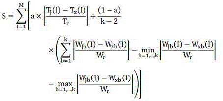
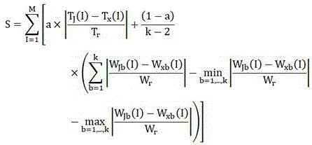
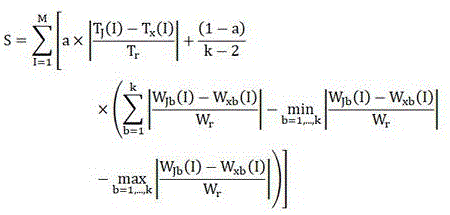
According to an implementable manner of the first aspect of the present application, the objective function is:
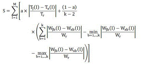
in the formula (I), the compound is shown in the specification, in order to be the objective function, the target function,
 for the number of boundary conditions to be set,
 in order to be the weight coefficient,
 a value range of
 ,
, Simplifying the model for the thermal resistance network in the second place
 The chip junction temperature under the boundary conditions,
 for detailed modeling in
 The chip junction temperature under the boundary conditions,
 for a preset recommended value of the chip junction temperature,
 for the number of surface nodes to be set,
 is at the first
 First in simplified model of thermal resistance network under individual boundary conditions
 The amount of heat flow at each node is,
 is at the first
 Detailed model under boundary conditions
 The amount of heat flow at each node is,
 is a preset difference threshold.
According to one possible implementation of the first aspect of the present application, before selecting the plurality of surface nodes from the detailed model of the chip, the method further comprises:
establishing a detailed model of the chip according to the parameters of the chip;
performing thermal simulation test on the detailed model to obtain a corresponding junction-shell thermal resistance simulation value;
and comparing the obtained junction-shell thermal resistance simulation value with a junction-shell thermal resistance reference value, and if the error between the obtained junction-shell thermal resistance simulation value and the junction-shell thermal resistance reference value exceeds a preset error threshold, correcting the detailed model until the error between the obtained junction-shell thermal resistance simulation value and the junction-shell thermal resistance reference value does not exceed the preset error threshold.
According to an implementable aspect of the first aspect of the present application, the performing thermal simulation testing on the detailed model includes:
setting boundary heat dissipation conditions of junction-shell thermal resistance test simulation;
and carrying out thermal simulation test on the detailed model according to the boundary heat dissipation condition.
According to a manner that can be realized by the first aspect of the present application, the setting of the boundary heat dissipation condition of the junction-case thermal resistance test simulation includes:
establishing a detailed model and a calculation domain of the chip in thermal simulation software, wherein the calculation domain wraps the detailed model, the upper surface of the calculation domain coincides with the upper surface of the chip, the lower surface of the calculation domain coincides with the bottom surface of the chip, and the peripheral surfaces of the calculation domain coincide with the peripheral surfaces of the chip, wherein the upper surface of the calculation domain is set as a boundary with a constant convective heat transfer coefficient, and the peripheral surfaces and the lower surface of the calculation domain are set as adiabatic boundary conditions.
A second aspect of the present application provides a simplified model modeling apparatus for a thermal resistance network, the apparatus including:
the device comprises a setting module, a calculation module and a control module, wherein the setting module is used for selecting a plurality of surface nodes from a detailed model of a chip and setting a network topology structure of a thermal resistance network simplified model according to the surface nodes;
the calculation module is used for setting a plurality of boundary conditions according to the application environment requirements of the chip and calculating the chip thermal parameter values of the detailed model under each boundary condition, wherein the chip thermal parameter values comprise chip nodes and heat flows passing through each surface node;
the construction module is used for constructing an objective function according to the chip thermal parameter values of the thermal resistance network simplified model and the detailed model under each boundary condition;
the thermal resistance network simplified model establishing module is used for taking the value of the target function as an optimization parameter, taking each thermal resistance value of the thermal resistance network simplified model as a quantity to be solved, obtaining a thermal resistance combination which enables the value of the target function to be minimum through optimization calculation, taking the thermal resistance combination as the value of the quantity to be solved, and establishing the thermal resistance network simplified model according to the thermal resistance combination;
and the simulation verification module is used for performing simulation comparison verification on the established thermal resistance network simplified model and the detailed model under a preset boundary condition, and outputting the established thermal resistance network simplified model when the difference value of the simulation junction temperatures output by the thermal resistance network simplified model and the detailed model does not exceed a preset temperature difference threshold value.
According to an implementable manner of the second aspect of the present application, the objective function is:
in the formula (I), the compound is shown in the specification, in order to be the objective function, the target function,
 for the number of boundary conditions to be set,
 in order to be the weight coefficient,
 a value range of
 ,
, Simplifying the model for the thermal resistance network in the second place
 The chip junction temperature under the boundary conditions,
 for detailed modeling in
 The chip junction temperature under the boundary conditions,
 for a preset recommended value of the chip junction temperature,
 for the number of surface nodes to be set,
 is at the first
 First in simplified model of thermal resistance network under individual boundary conditions
 The amount of heat flow at each node is,
 is at the first
 Detailed model under boundary conditions
 The amount of heat flow at each node is,
 is a preset difference threshold.
According to an implementable manner of the second aspect of the present application, the apparatus further comprises:
the detailed model establishing module is used for establishing a detailed model of the chip according to the parameters of the chip;
the detailed model simulation test module is used for carrying out thermal simulation test on the detailed model to obtain a corresponding junction-shell thermal resistance simulation value;
and the detailed model correction module is used for correcting the detailed model when the error between the obtained junction-shell thermal resistance simulation value and the junction-shell thermal resistance reference value exceeds a preset error threshold value until the error between the obtained junction-shell thermal resistance simulation value and the junction-shell thermal resistance reference value does not exceed the preset error threshold value.
According to an implementable manner of the second aspect of the present application, the detailed model simulation test module includes:
the boundary heat dissipation condition setting unit is used for setting boundary heat dissipation conditions of junction-shell thermal resistance test simulation;
and the thermal simulation test unit is used for carrying out thermal simulation test on the detailed model according to the boundary heat dissipation condition.
According to an implementable manner of the second aspect of the present application, the boundary heat dissipation condition setting unit specifically performs:
establishing a detailed model and a calculation domain of the chip in thermal simulation software, wherein the calculation domain wraps the detailed model, the upper surface of the calculation domain coincides with the upper surface of the chip, the lower surface of the calculation domain coincides with the bottom surface of the chip, and the peripheral surfaces of the calculation domain coincide with the peripheral surfaces of the chip, wherein the upper surface of the calculation domain is set as a boundary with a constant convective heat transfer coefficient, and the peripheral surfaces and the lower surface of the calculation domain are set as adiabatic boundary conditions.
A third aspect of the present application provides a thermal resistance network simplified model modeling apparatus, which includes a processor, a memory, and a computer program stored in the memory and configured to be executed by the processor, and the processor implements the thermal resistance network simplified model modeling method according to any one of the above items when executing the computer program.
A fourth aspect of the present application provides a computer-readable storage medium for storing a computer program for executing the simplified model modeling method of a thermal resistance network as described in any one of the above.
A fifth aspect of the present application provides a method for predicting a junction temperature of a chip, where the method includes:
and introducing the simplified model of the thermal resistance network into a server device simulating an actual working environment for simulation, and outputting a junction temperature result of a chip in the server device.
Compared with the prior art, the application has at least the following beneficial technical effects:
according to the method, the target function is constructed according to the thermal resistance network simplified model and the detailed model under the set chip thermal parameter values under each boundary condition, optimization is carried out based on the target function so as to obtain the thermal resistance combination which enables the value of the target function to be minimum, then the thermal resistance network simplified model is established according to the thermal resistance combination and simulation verification is carried out, the obtained thermal resistance network simplified model can be close to a solid chip, and the modeling efficiency and accuracy of the thermal resistance network simplified model are improved; the simplified model of the thermal resistance network is led into a server device simulating the actual working environment for simulation, so that the high-precision prediction of the junction temperature of the chip can be realized.
Drawings
FIG. 1 is a schematic flow chart diagram illustrating an alternative embodiment of a simplified model modeling method for a thermal resistance network provided herein;
FIG. 2 is a schematic diagram of an alternative embodiment of boundary conditions for the case thermal resistance simulation provided herein;
FIG. 3 is a schematic diagram of another alternative embodiment of boundary conditions for a case thermal resistance simulation provided herein;
FIG. 4 is a schematic structural connection diagram of an alternative embodiment of a simplified model modeling apparatus for a thermal resistance network provided by the present application.
Reference numerals:
1. setting a module; 2. a calculation module; 3. building a module; 4. a thermal resistance network simplified model building module; 5. and a simulation verification module.
Detailed Description
The technical solutions in the embodiments of the present application will be clearly and completely described below with reference to the drawings in the embodiments of the present application, and it is obvious that the described embodiments are only a part of the embodiments of the present application, and not all of the embodiments. All other embodiments, which can be derived by a person skilled in the art from the embodiments given herein without making any creative effort, shall fall within the protection scope of the present application.
Fig. 1 is a schematic flow chart of an alternative embodiment of a simplified modeling method for a thermal resistance network according to the present application.
As shown in fig. 1, the method includes:
s1: selecting a plurality of surface nodes from a detailed model of a chip, and setting a network topological structure of a thermal resistance network simplified model according to the surface nodes;
s2: setting a plurality of boundary conditions according to the application environment requirements of the chip, and calculating the chip thermal parameter values of the detailed model under each boundary condition, wherein the chip thermal parameter values comprise chip nodes and heat flows passing through each surface node;
s3: constructing an objective function according to the thermal resistance network simplified model and the detailed model under each chip thermal parameter value under the boundary condition;
s4: taking the value of the target function as an optimization parameter, taking each thermal resistance value of the thermal resistance network simplified model as a quantity to be solved, obtaining a thermal resistance combination which enables the value of the target function to be minimum through optimization calculation, taking the thermal resistance combination as the value of the quantity to be solved, and establishing the thermal resistance network simplified model according to the thermal resistance combination;
s5: and carrying out simulation comparison verification on the established thermal resistance network simplified model and the detailed model under a preset boundary condition, and outputting the established thermal resistance network simplified model when the difference value of the simulated junction temperatures output by the thermal resistance network simplified model and the detailed model does not exceed a preset temperature difference threshold value.
The thermal resistance network simplified model adopts a fixed thermal resistance network expression to represent the thermal performance of the chip under the boundary condition, the thermal resistance value of the thermal resistance network simplified model is determined by setting the objective function, the modeling efficiency of the thermal resistance network simplified model is improved, the junction temperature of the chip is predicted by the thermal resistance network simplified model, and the effective prediction of the junction temperature of the chip can be realized.
When multiple sets of boundary conditions are set according to the application environment requirements of the chip, the boundary conditions corresponding to the application environments that the chip may encounter can be selected from 58 boundary conditions proposed in JEDEC (solid state technology association) standards.
In one embodiment, the network topology structure of the simplified model of the thermal resistance network is a star-shaped structure, the corresponding surface nodes include four nodes representing a top surface, a side surface, a bottom surface and pins, which are connected with the chip nodes, and the nodes are connected with the chip nodes through thermal resistances respectively representing the heat dissipation effect of the top surface, the side surface, the bottom surface and the pins on the chip.
In another embodiment, the network topology of the simplified model of the thermal resistance network is a Delphi node topology, and the corresponding surface nodes include five nodes representing a top surface inner side, a top surface outer side, a bottom surface inner side, a bottom surface outer side and pins connected to the chip nodes. Further, the corresponding surface nodes of the Delphi node topology may also include at least one node representing a side. Each node is connected with the chip node through a thermal resistor, and a thermal resistor can be arranged between the surface nodes.
In one embodiment, the objective function is:
in the formula (I), the compound is shown in the specification, is an objective function,
 For the number of boundary conditions to be set,
 in order to be the weight coefficient,
 a value range of
 ,
, Simplifying the model for the thermal resistance network in the second place
 The chip junction temperature under the boundary conditions,
 for detailed modeling in
 The chip junction temperature under the boundary conditions,
 for a preset recommended value of the chip junction temperature,
 for the number of surface nodes to be set,
 is at the first
 First in simplified model of thermal resistance network under individual boundary conditions
 The amount of heat flow at each node is,
 is at the first
 Detailed model under boundary conditions
 The amount of heat flow at each node is,
 is a preset difference threshold.
According to the thermal resistance network simplified model and the detailed model, the specific function formula of the objective function is designed according to the chip thermal parameter values under the boundary conditions.
In some embodiments, prior to selecting the plurality of surface nodes from the detailed model of the chip, the method further comprises:
establishing a detailed model of the chip according to the parameters of the chip;
performing thermal simulation test on the detailed model to obtain a corresponding junction-shell thermal resistance simulation value;
and comparing the obtained junction-shell thermal resistance simulation value with a junction-shell thermal resistance reference value, and if the error between the obtained junction-shell thermal resistance simulation value and the junction-shell thermal resistance reference value exceeds a preset error threshold, correcting the detailed model until the error between the obtained junction-shell thermal resistance simulation value and the junction-shell thermal resistance reference value does not exceed the preset error threshold.
The parameters of the chip comprise structure size parameters, material parameters and thermal conductivity of the chip.
And if the error between the junction-shell thermal resistance simulation value and the junction-shell thermal resistance reference value does not exceed a preset error threshold value, the detailed model is a verified effective model, and surface nodes can be selected according to the detailed model. The accuracy of the detailed model influences the accuracy of the simplified model of the chip thermal resistance network, and the method and the device verify the detailed model by using the junction-shell thermal resistance to ensure the correctness of the detailed model, thereby laying a good foundation for the accurate modeling of the simplified model of the chip thermal resistance network.
In one embodiment, the performing thermal simulation testing on the detailed model includes:
setting boundary heat dissipation conditions of junction-shell thermal resistance test simulation;
and carrying out thermal simulation test on the detailed model according to the boundary heat dissipation condition.
According to the JEDEC standard, when calculating junction-shell thermal resistance of a chip, a boundary heat dissipation condition is set to promote as much heat generated by the operation of the chip as possible to be transferred to a mounting surface of a heat sink, which is an upper surface case of the chip for the chip, and to dissipate heat to the environment through the surface.
In an alternative embodiment, the setting of the boundary heat dissipation condition of the junction-case thermal resistance test simulation includes:
establishing a detailed model and a calculation domain of the chip in thermal simulation software, establishing a cold plate above a chip shell, wrapping the chip and the cold plate in the calculation domain, enabling the upper surface of the cold plate to be superposed with the upper surface of the calculation domain, enabling the periphery of the cold plate to be superposed with the peripheral surface of the calculation domain, enabling the bottom surface of the chip to be superposed with the lower surface of the calculation domain, and filling the part except the solid in the calculation domain with air, as shown in fig. 2.
The temperature of the cold plate is set to be the same as the ambient temperature, so that the heat conducted to the cold plate by the chip can be absorbed infinitely; the periphery and the bottom surface of the calculation domain are set to be heat insulation boundaries, and at the moment, the heat of the chip cannot be transferred to the outside from the periphery and the bottom surface; through the above boundary arrangement, the heat of the chip can be conducted to the cold plate only through the upper surface for heat dissipation
In another alternative, the setting junction-shell thermal resistance Testing simulated boundary heat dissipation conditions, comprising:
establishing a detailed model and a calculation domain of the chip in thermal simulation software, wherein the calculation domain wraps the detailed model, the upper surface of the calculation domain coincides with the upper surface of the chip, the lower surface of the calculation domain coincides with the bottom surface of the chip, and the peripheral surfaces of the calculation domain coincide with the peripheral surfaces of the chip, wherein the upper surface of the calculation domain is set as a boundary with a constant convective heat transfer coefficient, and the peripheral surfaces and the lower surface of the calculation domain are set as adiabatic boundary conditions, as shown in fig. 3.
The boundary heat dissipation condition can promote the heat of the chip to be conducted to the upper surface of the chip as much as possible.
In one embodiment, the convective heat transfer coefficient is set to a value W/(k·m)。
Wherein W/(k.m) is a unit of thermal conductivity, "k" is an absolute temperature unit and can be replaced by "C", "W" means a unit of thermal power, "m" means a unit of length meter.
The convection heat transfer coefficient magnitude is very large, the periphery and the lower surface of the calculation domain are set to be thermal insulation boundary conditions to prevent the heat of the chip from being transferred to the bottom surface and the periphery, the heat of the chip can be promoted to be conducted to the upper surface as much as possible, and the accuracy of junction-shell thermal resistance testing is improved.
The thermal simulation software described above may employ finite element analysis software.
The embodiment of the second aspect of the application provides a thermal resistance network simplified model modeling device.
Fig. 4 is a schematic structural diagram of an alternative embodiment of the simplified model modeling apparatus for a thermal resistance network provided in the present application, which is capable of implementing the entire process of the simplified model modeling method for a thermal resistance network according to any one of the embodiments.
As shown in fig. 4, the apparatus includes:
the device comprises a setting module 1, a calculation module and a control module, wherein the setting module 1 is used for selecting a plurality of surface nodes from a detailed model of a chip and setting a network topology structure of a thermal resistance network simplified model according to the surface nodes;
the calculation module 2 is configured to set a plurality of boundary conditions according to the application environment requirements of the chip, and calculate chip thermal parameter values of the detailed model under each of the boundary conditions, where the chip thermal parameter values include a chip junction temperature and a thermal flow passing through each surface node;
the building module 3 is used for building an objective function according to the chip thermal parameter values of the thermal resistance network simplified model and the detailed model under each boundary condition;
the thermal resistance network simplified model establishing module 4 is used for taking the value of the target function as an optimization parameter, taking each thermal resistance value of the thermal resistance network simplified model as a quantity to be solved, obtaining a thermal resistance combination which enables the value of the target function to be minimum through optimization calculation, taking the thermal resistance combination as the value of the quantity to be solved, and establishing the thermal resistance network simplified model according to the thermal resistance combination;
and the simulation verification module 5 is used for performing simulation comparison verification on the established thermal resistance network simplified model and the detailed model under a preset boundary condition, and outputting the established thermal resistance network simplified model when the difference value of the simulation junction temperatures output by the thermal resistance network simplified model and the detailed model does not exceed a preset temperature difference threshold value.
In an alternative embodiment, the objective function is:
in the formula (I), the compound is shown in the specification, in order to be the objective function, the target function,
 for the number of boundary conditions to be set,
 in order to be the weight coefficient,
 a value range of
 ,
, Simplifying the model for the thermal resistance network in the second place
 The chip junction temperature under the boundary conditions,
 for detailed modeling in
 The chip junction temperature under the boundary conditions,
 for a preset recommended value of the chip junction temperature,
 for the number of surface nodes to be set,
 is at the first
 First in simplified model of thermal resistance network under individual boundary conditions
 The amount of heat flow at each node is,
 is at the first
 Detailed model under boundary conditions
 The amount of heat flow at each node is,
 is presetAnd (4) a difference threshold value.
In an alternative embodiment, the apparatus further comprises:
the detailed model establishing module is used for establishing a detailed model of the chip according to the parameters of the chip;
the detailed model simulation test module is used for carrying out thermal simulation test on the detailed model to obtain a corresponding junction-shell thermal resistance simulation value;
and the detailed model correction module is used for correcting the detailed model when the error between the obtained junction-shell thermal resistance simulation value and the junction-shell thermal resistance reference value exceeds a preset error threshold value until the error between the obtained junction-shell thermal resistance simulation value and the junction-shell thermal resistance reference value does not exceed the preset error threshold value.
In an alternative embodiment, the detailed model simulation test module includes:
the boundary heat dissipation condition setting unit is used for setting boundary heat dissipation conditions of junction-shell thermal resistance test simulation;
and the thermal simulation test unit is used for carrying out thermal simulation test on the detailed model according to the boundary heat dissipation condition.
In an optional implementation manner, the boundary heat dissipation condition setting unit specifically executes:
establishing a detailed model and a calculation domain of the chip in thermal simulation software, establishing a cold plate above a chip shell, wrapping the chip and the cold plate in the calculation domain, enabling the upper surface of the cold plate to be superposed with the upper surface of the calculation domain, enabling the periphery of the cold plate to be superposed with the peripheral surface of the calculation domain, enabling the bottom surface of the chip to be superposed with the lower surface of the calculation domain, and filling the part except the solid in the calculation domain with air.
In another optional implementation, the boundary heat dissipation condition setting unit specifically executes:
establishing a detailed model and a calculation domain of the chip in thermal simulation software, wherein the calculation domain wraps the detailed model, the upper surface of the calculation domain coincides with the upper surface of the chip, the lower surface of the calculation domain coincides with the bottom surface of the chip, and the peripheral surfaces of the calculation domain coincide with the peripheral surfaces of the chip, wherein the upper surface of the calculation domain is set as a boundary with a constant convective heat transfer coefficient, and the peripheral surfaces and the lower surface of the calculation domain are set as adiabatic boundary conditions.
In a third aspect of the present application, an embodiment provides a thermal resistance network simplified model modeling apparatus, which includes a processor, a memory, and a computer program stored in the memory and configured to be executed by the processor, and when the processor executes the computer program, the thermal resistance network simplified model modeling method as described in any one of the above is implemented.
An embodiment of a fourth aspect of the present application provides a computer-readable storage medium for storing a computer program for executing the simplified modeling method of the thermal resistance network according to any one of the above.
In a fifth aspect of the present application, a method for predicting a junction temperature of a chip is provided, where the method includes:
and introducing the thermal resistance network simplified model into a server system simulating an actual working environment for simulation, and outputting a junction temperature result of a chip in the server system.
It should be noted that the Processor may be a Central Processing Unit (chip), other general-purpose Processor, a Digital Signal Processor (DSP), an Application Specific Integrated Circuit (ASIC), a Field-Programmable Gate Array (FPGA) or other Programmable logic device, a discrete Gate or transistor logic device, a discrete hardware component, and the like. The general processor can be a microprocessor or the processor can be any conventional processor and the like, the processor is a control center of the thermal resistance network simplified model modeling device, and various interfaces and lines are utilized to connect various parts of the whole thermal resistance network simplified model modeling device.
The memory may be used to store the computer program and/or module, and the processor may implement various functions of the thermal resistance network simplified model modeling apparatus by executing or executing the computer program and/or module stored in the memory and calling data stored in the memory. The memory may mainly include a storage program area and a storage data area, wherein the storage program area may store an operating device, an application program required by at least one function (such as a sound playing function, an image playing function, etc.), and the like; the storage data area may store data (such as audio data, a phonebook, etc.) created according to the use of the cellular phone, and the like. In addition, the memory may include high speed random access memory, and may also include non-volatile memory, such as a hard disk, a memory, a plug-in hard disk, a Smart Media Card (SMC), a Secure Digital (SD) Card, a Flash memory Card (Flash Card), at least one magnetic disk storage device, a Flash memory device, or other volatile solid state storage device.
Wherein, the modules/units integrated by the thermal resistance network simplified model modeling device can be stored in a computer readable storage medium if the modules/units are realized in the form of software functional units and sold or used as independent products. Based on such understanding, all or part of the flow in the method of the embodiments described above can be realized by a computer program, which can be stored in a computer-readable storage medium and can realize the steps of the embodiments of the methods described above when the computer program is executed by a processor. Wherein the computer program comprises computer program code, which may be in the form of source code, object code, an executable file or some intermediate form, etc. The computer-readable medium may include: any entity or device capable of carrying the computer program code, recording medium, usb disk, removable hard disk, magnetic disk, optical disk, computer Memory, Read-Only Memory (ROM), Random Access Memory (RAM), electrical carrier wave signals, telecommunications signals, software distribution medium, and the like.
While the foregoing is directed to alternative embodiments of the present application, it will be appreciated by those skilled in the art that various changes and modifications may be made without departing from the principles of the application, and that such changes and modifications are to be considered as within the scope of the application.
Claims (13)
1. A method for modeling a simplified model of a thermal resistance network, the method comprising:
selecting a plurality of surface nodes from a detailed model of a chip, and setting a network topological structure of a thermal resistance network simplified model according to the surface nodes;
setting a plurality of boundary conditions according to the application environment requirements of the chip, and calculating the chip thermal parameter values of the detailed model under each boundary condition, wherein the chip thermal parameter values comprise chip nodes and heat flows passing through each surface node;
constructing an objective function according to the thermal resistance network simplified model and the detailed model under each chip thermal parameter value under the boundary condition;
taking the value of the target function as an optimization parameter, taking each thermal resistance value of the thermal resistance network simplified model as a quantity to be solved, obtaining a thermal resistance combination which enables the value of the target function to be minimum through optimization calculation, taking the thermal resistance combination as the value of the quantity to be solved, and establishing the thermal resistance network simplified model according to the thermal resistance combination;
and carrying out simulation comparison verification on the established thermal resistance network simplified model and the detailed model under a preset boundary condition, and outputting the established thermal resistance network simplified model when the difference value of the simulated junction temperatures output by the thermal resistance network simplified model and the detailed model does not exceed a preset temperature difference threshold value.
2. The method of modeling a simplified model of a thermal resistance network as claimed in claim 1 wherein the objective function is:

in the formula (I), the compound is shown in the specification, in order to be the objective function, the target function,
 for the number of boundary conditions to be set,
 in order to be the weight coefficient,
 a value range of
 ,
, Simplifying the model for the thermal resistance network in the second place
 The chip junction temperature under the boundary conditions,
 for detailed modeling in
 The chip junction temperature under the boundary conditions,
 for a preset recommended value of the chip junction temperature,
 for the number of surface nodes to be set,
 is at the first
 Thermal resistance network simple under boundary conditionChange the model to
 The amount of heat flow at each node is,
 is at the first
 Detailed model under boundary conditions
 The amount of heat flow at each node is,
 is a preset difference threshold.
3. The method of claim 1, wherein prior to selecting the plurality of surface nodes from the detailed model of the chip, the method further comprises:
establishing a detailed model of the chip according to the parameters of the chip;
performing thermal simulation test on the detailed model to obtain a corresponding junction-shell thermal resistance simulation value;
and comparing the obtained junction-shell thermal resistance simulation value with a junction-shell thermal resistance reference value, and if the error between the obtained junction-shell thermal resistance simulation value and the junction-shell thermal resistance reference value exceeds a preset error threshold, correcting the detailed model until the error between the obtained junction-shell thermal resistance simulation value and the junction-shell thermal resistance reference value does not exceed the preset error threshold.
4. The method of claim 3, wherein the performing thermal simulation testing on the detailed model comprises:
setting boundary heat dissipation conditions of junction-shell thermal resistance test simulation;
and carrying out thermal simulation test on the detailed model according to the boundary heat dissipation condition.
5. The modeling method of the thermal resistance network simplified model according to claim 4, wherein the setting of boundary heat dissipation conditions of junction-shell thermal resistance test simulation comprises:
establishing a detailed model and a calculation domain of the chip in thermal simulation software, wherein the calculation domain wraps the detailed model, the upper surface of the calculation domain coincides with the upper surface of the chip, the lower surface of the calculation domain coincides with the bottom surface of the chip, and the peripheral surfaces of the calculation domain coincide with the peripheral surfaces of the chip, wherein the upper surface of the calculation domain is set as a boundary with a constant convective heat transfer coefficient, and the peripheral surfaces and the lower surface of the calculation domain are set as adiabatic boundary conditions.
6. A thermal resistance network simplified model modeling apparatus, the apparatus comprising:
the device comprises a setting module, a calculation module and a control module, wherein the setting module is used for selecting a plurality of surface nodes from a detailed model of a chip and setting a network topology structure of a thermal resistance network simplified model according to the surface nodes;
the calculation module is used for setting a plurality of boundary conditions according to the application environment requirements of the chip and calculating the chip thermal parameter values of the detailed model under each boundary condition, wherein the chip thermal parameter values comprise chip nodes and heat flows passing through each surface node;
the construction module is used for constructing an objective function according to the chip thermal parameter values of the thermal resistance network simplified model and the detailed model under each boundary condition;
the thermal resistance network simplified model establishing module is used for taking the value of the target function as an optimization parameter, taking each thermal resistance value of the thermal resistance network simplified model as a quantity to be solved, obtaining a thermal resistance combination which enables the value of the target function to be minimum through optimization calculation, taking the thermal resistance combination as the value of the quantity to be solved, and establishing the thermal resistance network simplified model according to the thermal resistance combination;
and the simulation verification module is used for performing simulation comparison verification on the established thermal resistance network simplified model and the detailed model under a preset boundary condition, and outputting the established thermal resistance network simplified model when the difference value of the simulation junction temperatures output by the thermal resistance network simplified model and the detailed model does not exceed a preset temperature difference threshold value.
7. The simplified model modeling apparatus for thermal resistance network as claimed in claim 6, wherein said objective function is:

in the formula (I), the compound is shown in the specification, in order to be the objective function, the target function,
 for the number of boundary conditions to be set,
 in order to be the weight coefficient,
 a value range of
 ,
, Simplifying the model for the thermal resistance network in the second place
 The chip junction temperature under the boundary conditions,
 for detailed modeling in
 The chip junction temperature under the boundary conditions,
 for a preset recommended value of the chip junction temperature,
 for the number of surface nodes to be set,
 is at the first
 First in simplified model of thermal resistance network under individual boundary conditions
 The amount of heat flow at each node is,
 is at the first
 Detailed model under boundary conditions
 The amount of heat flow at each node is,
 is a preset difference threshold.
8. The simplified model modeling apparatus for thermal resistance network as claimed in claim 6, wherein said apparatus further comprises:
the detailed model establishing module is used for establishing a detailed model of the chip according to the parameters of the chip;
the detailed model simulation test module is used for carrying out thermal simulation test on the detailed model to obtain a corresponding junction-shell thermal resistance simulation value;
and the detailed model correction module is used for correcting the detailed model when the error between the obtained junction-shell thermal resistance simulation value and the junction-shell thermal resistance reference value exceeds a preset error threshold value until the error between the obtained junction-shell thermal resistance simulation value and the junction-shell thermal resistance reference value does not exceed the preset error threshold value.
9. The thermal resistance network simplified model modeling apparatus of claim 8, wherein the detailed model simulation test module comprises:
the boundary heat dissipation condition setting unit is used for setting boundary heat dissipation conditions of junction-shell thermal resistance test simulation;
and the thermal simulation test unit is used for carrying out thermal simulation test on the detailed model according to the boundary heat dissipation condition.
10. The modeling apparatus of the simplified thermal resistance network model according to claim 9, wherein the boundary heat dissipation condition setting unit specifically performs:
establishing a detailed model and a calculation domain of the chip in thermal simulation software, wherein the calculation domain wraps the detailed model, the upper surface of the calculation domain coincides with the upper surface of the chip, the lower surface of the calculation domain coincides with the bottom surface of the chip, and the peripheral surfaces of the calculation domain coincide with the peripheral surfaces of the chip, wherein the upper surface of the calculation domain is set as a boundary with a constant convective heat transfer coefficient, and the peripheral surfaces and the lower surface of the calculation domain are set as adiabatic boundary conditions.
11. A thermal resistance network simplified model modeling apparatus, comprising a processor, a memory, and a computer program stored in the memory and configured to be executed by the processor, the processor implementing the thermal resistance network simplified model modeling method according to any one of claims 1 to 5 when executing the computer program.
12. A computer-readable storage medium for storing a computer program for executing the simplified modeling method of a thermal resistance network according to any one of claims 1 to 5.
13. A method for predicting chip junction temperature, the method comprising:
the simplified model of the thermal resistance network as claimed in any one of claims 1 to 5 is introduced into a server device for simulating an actual working environment, and a junction temperature result of a chip in the server device is output.
Priority Applications (1)
| Application Number | Priority Date | Filing Date | Title |
|---|---|---|---|
| CN202111317957.5A CN113779742B (en) | 2021-11-09 | 2021-11-09 | Modeling method and device for simplified model of thermal resistance network and chip junction temperature prediction method |
Applications Claiming Priority (1)
| Application Number | Priority Date | Filing Date | Title |
|---|---|---|---|
| CN202111317957.5A CN113779742B (en) | 2021-11-09 | 2021-11-09 | Modeling method and device for simplified model of thermal resistance network and chip junction temperature prediction method |
Publications (2)
| Publication Number | Publication Date |
|---|---|
| CN113779742A true CN113779742A (en) | 2021-12-10 |
| CN113779742B CN113779742B (en) | 2022-03-04 |
Family
ID=78956897
Family Applications (1)
| Application Number | Title | Priority Date | Filing Date |
|---|---|---|---|
| CN202111317957.5A Active CN113779742B (en) | 2021-11-09 | 2021-11-09 | Modeling method and device for simplified model of thermal resistance network and chip junction temperature prediction method |
Country Status (1)
| Country | Link |
|---|---|
| CN (1) | CN113779742B (en) |
Cited By (3)
| Publication number | Priority date | Publication date | Assignee | Title |
|---|---|---|---|---|
| CN114330180A (en) * | 2021-12-30 | 2022-04-12 | 广东芯聚能半导体有限公司 | Chip packaging method and device, computer equipment and storage medium |
| CN115345119A (en) * | 2022-07-29 | 2022-11-15 | 深圳市紫光同创电子有限公司 | Method for predicting cold time of chip |
| CN116484777A (en) * | 2023-06-19 | 2023-07-25 | 湖南大学 | Thermal network model modeling and chip temperature calculation method, equipment and storage medium |
Citations (8)
| Publication number | Priority date | Publication date | Assignee | Title |
|---|---|---|---|---|
| CN101017510A (en) * | 2006-03-13 | 2007-08-15 | 信息产业部电子第五研究所 | Heat resistance network model and method for calculating junction temperature of microelectronics using same |
| CN103345563A (en) * | 2013-07-19 | 2013-10-09 | 郑州大学 | Micro-channel minimum thermal resistance structure optimization method based on access development characteristics |
| WO2015021726A1 (en) * | 2013-08-13 | 2015-02-19 | 杭州远方光电信息股份有限公司 | Thermal resistance analysis method |
| US20190188357A1 (en) * | 2017-12-15 | 2019-06-20 | Industrial Technology Research Institute | Chip temperature computation method and chip temperature computation device |
| CN110416105A (en) * | 2019-07-29 | 2019-11-05 | 闽南师范大学 | A kind of illuminant characterization parameter determination method and system for photoelectric conversion |
| CN110728025A (en) * | 2019-09-16 | 2020-01-24 | 中国振华集团永光电子有限公司(国营第八七三厂) | Method for calculating thermal resistance of Schottky module packaged diode |
| CN112464358A (en) * | 2020-10-27 | 2021-03-09 | 中国运载火箭技术研究院 | Method, device, terminal and medium for evaluating environmental temperature of carrier rocket equipment |
| CN113158601A (en) * | 2021-03-24 | 2021-07-23 | 复旦大学 | High-reliability board-level fan-out SiC MOSFET packaging structure optimization method |
-
2021
- 2021-11-09 CN CN202111317957.5A patent/CN113779742B/en active Active
Patent Citations (8)
| Publication number | Priority date | Publication date | Assignee | Title |
|---|---|---|---|---|
| CN101017510A (en) * | 2006-03-13 | 2007-08-15 | 信息产业部电子第五研究所 | Heat resistance network model and method for calculating junction temperature of microelectronics using same |
| CN103345563A (en) * | 2013-07-19 | 2013-10-09 | 郑州大学 | Micro-channel minimum thermal resistance structure optimization method based on access development characteristics |
| WO2015021726A1 (en) * | 2013-08-13 | 2015-02-19 | 杭州远方光电信息股份有限公司 | Thermal resistance analysis method |
| US20190188357A1 (en) * | 2017-12-15 | 2019-06-20 | Industrial Technology Research Institute | Chip temperature computation method and chip temperature computation device |
| CN110416105A (en) * | 2019-07-29 | 2019-11-05 | 闽南师范大学 | A kind of illuminant characterization parameter determination method and system for photoelectric conversion |
| CN110728025A (en) * | 2019-09-16 | 2020-01-24 | 中国振华集团永光电子有限公司(国营第八七三厂) | Method for calculating thermal resistance of Schottky module packaged diode |
| CN112464358A (en) * | 2020-10-27 | 2021-03-09 | 中国运载火箭技术研究院 | Method, device, terminal and medium for evaluating environmental temperature of carrier rocket equipment |
| CN113158601A (en) * | 2021-03-24 | 2021-07-23 | 复旦大学 | High-reliability board-level fan-out SiC MOSFET packaging structure optimization method |
Non-Patent Citations (1)
| Title |
|---|
| 何成: "典型封装芯片的热阻网络模型研究", 《中国优秀博硕士学位论文全文数据库(硕士)信息科技辑》 * |
Cited By (4)
| Publication number | Priority date | Publication date | Assignee | Title |
|---|---|---|---|---|
| CN114330180A (en) * | 2021-12-30 | 2022-04-12 | 广东芯聚能半导体有限公司 | Chip packaging method and device, computer equipment and storage medium |
| CN115345119A (en) * | 2022-07-29 | 2022-11-15 | 深圳市紫光同创电子有限公司 | Method for predicting cold time of chip |
| CN116484777A (en) * | 2023-06-19 | 2023-07-25 | 湖南大学 | Thermal network model modeling and chip temperature calculation method, equipment and storage medium |
| CN116484777B (en) * | 2023-06-19 | 2023-10-13 | 湖南大学 | Thermal network model modeling and chip temperature calculating method, device and storage medium |
Also Published As
| Publication number | Publication date |
|---|---|
| CN113779742B (en) | 2022-03-04 |
Similar Documents
| Publication | Publication Date | Title |
|---|---|---|
| CN113779742B (en) | Modeling method and device for simplified model of thermal resistance network and chip junction temperature prediction method | |
| CN111125947B (en) | A press-bonded IGBT thermal network model modeling method and related devices | |
| CN112307656B (en) | Method, system and device for acquiring electrothermal parameters of power semiconductor module | |
| US9135383B2 (en) | Table model circuit simulation acceleration using model caching | |
| CN119066878B (en) | A method, apparatus, equipment and medium for constructing a multiphysics proxy model for an electric motor | |
| CN116432571A (en) | Chip thermal simulation method, system, equipment and medium | |
| CN114781201B (en) | A method, system, device and medium for calculating PCB temperature field in radiator | |
| CN117309930A (en) | Method, device, equipment, medium and program product for estimating chip junction temperature | |
| CN112199835A (en) | Method, device and terminal equipment for determining temperature rise of cable group | |
| CN116611181A (en) | Flow thermal coupling analysis method, system, equipment and medium for turbine casing structure | |
| CN113408110B (en) | Solder point temperature prediction method, device, readable storage medium and electronic device | |
| CN113865734B (en) | Temperature sensor model creating method and device and electronic equipment | |
| WO2019176282A1 (en) | Thermal analysis model of resistor, thermal analyzer for same, thermal analysis program and model generation program | |
| CN115048841B (en) | Electrothermal coupling analysis method and simulation terminal for passive circuits | |
| CN117034658B (en) | Calculation method for transient thermal simulation of core particle packaging structure | |
| CN113971341B (en) | Optimization method, device and thermal resistance network model of chip thermal resistance network model | |
| CN119538840A (en) | Printed circuit board electrothermal simulation processing method, device, equipment and storage medium | |
| Maggioni et al. | Fast transient convolution-based thermal modeling methodology for including the package thermal impact in 3D ICs | |
| CN117668412A (en) | A method and device for determining junction temperature | |
| CN116720340A (en) | Correction method and device for convective heat transfer coefficient, terminal and storage medium | |
| CN117494656B (en) | A chip junction temperature and thermal resistance model modeling method and device | |
| CN114330182A (en) | Method and device for simulating chip heating and chip heating simulation system | |
| CN118690720B (en) | Method and system for testing stability of chip modeling component based on production operation | |
| CN120930323A (en) | Thermal simulation method, device and equipment for power device and storage medium | |
| CN114354681B (en) | Device and method for simulating chip thermal resistance |
Legal Events
| Date | Code | Title | Description |
|---|---|---|---|
| PB01 | Publication | ||
| PB01 | Publication | ||
| SE01 | Entry into force of request for substantive examination | ||
| SE01 | Entry into force of request for substantive examination | ||
| GR01 | Patent grant | ||
| GR01 | Patent grant |