CN113711189A - System and method for managing reduced power failure energy requirements on solid state drives - Google Patents
System and method for managing reduced power failure energy requirements on solid state drives Download PDFInfo
- Publication number
- CN113711189A CN113711189A CN202080026771.1A CN202080026771A CN113711189A CN 113711189 A CN113711189 A CN 113711189A CN 202080026771 A CN202080026771 A CN 202080026771A CN 113711189 A CN113711189 A CN 113711189A
- Authority
- CN
- China
- Prior art keywords
- write commands
- ssd
- volatile memory
- unexecuted
- power failure
- Prior art date
- Legal status (The legal status is an assumption and is not a legal conclusion. Google has not performed a legal analysis and makes no representation as to the accuracy of the status listed.)
- Granted
Links
Images


Classifications
-
- G—PHYSICS
- G06—COMPUTING OR CALCULATING; COUNTING
- G06F—ELECTRIC DIGITAL DATA PROCESSING
- G06F11/00—Error detection; Error correction; Monitoring
- G06F11/07—Responding to the occurrence of a fault, e.g. fault tolerance
- G06F11/14—Error detection or correction of the data by redundancy in operation
- G06F11/1402—Saving, restoring, recovering or retrying
- G06F11/1415—Saving, restoring, recovering or retrying at system level
- G06F11/1441—Resetting or repowering
-
- G—PHYSICS
- G06—COMPUTING OR CALCULATING; COUNTING
- G06F—ELECTRIC DIGITAL DATA PROCESSING
- G06F1/00—Details not covered by groups G06F3/00 - G06F13/00 and G06F21/00
- G06F1/26—Power supply means, e.g. regulation thereof
- G06F1/30—Means for acting in the event of power-supply failure or interruption, e.g. power-supply fluctuations
-
- G—PHYSICS
- G06—COMPUTING OR CALCULATING; COUNTING
- G06F—ELECTRIC DIGITAL DATA PROCESSING
- G06F1/00—Details not covered by groups G06F3/00 - G06F13/00 and G06F21/00
- G06F1/26—Power supply means, e.g. regulation thereof
- G06F1/32—Means for saving power
- G06F1/3203—Power management, i.e. event-based initiation of a power-saving mode
- G06F1/3206—Monitoring of events, devices or parameters that trigger a change in power modality
- G06F1/3215—Monitoring of peripheral devices
- G06F1/3225—Monitoring of peripheral devices of memory devices
-
- G—PHYSICS
- G06—COMPUTING OR CALCULATING; COUNTING
- G06F—ELECTRIC DIGITAL DATA PROCESSING
- G06F11/00—Error detection; Error correction; Monitoring
- G06F11/07—Responding to the occurrence of a fault, e.g. fault tolerance
- G06F11/16—Error detection or correction of the data by redundancy in hardware
- G06F11/20—Error detection or correction of the data by redundancy in hardware using active fault-masking, e.g. by switching out faulty elements or by switching in spare elements
- G06F11/2015—Redundant power supplies
-
- G—PHYSICS
- G06—COMPUTING OR CALCULATING; COUNTING
- G06F—ELECTRIC DIGITAL DATA PROCESSING
- G06F11/00—Error detection; Error correction; Monitoring
- G06F11/30—Monitoring
- G06F11/3003—Monitoring arrangements specially adapted to the computing system or computing system component being monitored
- G06F11/3034—Monitoring arrangements specially adapted to the computing system or computing system component being monitored where the computing system component is a storage system, e.g. DASD based or network based
-
- G—PHYSICS
- G06—COMPUTING OR CALCULATING; COUNTING
- G06F—ELECTRIC DIGITAL DATA PROCESSING
- G06F3/00—Input arrangements for transferring data to be processed into a form capable of being handled by the computer; Output arrangements for transferring data from processing unit to output unit, e.g. interface arrangements
- G06F3/06—Digital input from, or digital output to, record carriers, e.g. RAID, emulated record carriers or networked record carriers
- G06F3/0601—Interfaces specially adapted for storage systems
- G06F3/0602—Interfaces specially adapted for storage systems specifically adapted to achieve a particular effect
- G06F3/0614—Improving the reliability of storage systems
- G06F3/0619—Improving the reliability of storage systems in relation to data integrity, e.g. data losses, bit errors
-
- G—PHYSICS
- G06—COMPUTING OR CALCULATING; COUNTING
- G06F—ELECTRIC DIGITAL DATA PROCESSING
- G06F3/00—Input arrangements for transferring data to be processed into a form capable of being handled by the computer; Output arrangements for transferring data from processing unit to output unit, e.g. interface arrangements
- G06F3/06—Digital input from, or digital output to, record carriers, e.g. RAID, emulated record carriers or networked record carriers
- G06F3/0601—Interfaces specially adapted for storage systems
- G06F3/0628—Interfaces specially adapted for storage systems making use of a particular technique
- G06F3/0655—Vertical data movement, i.e. input-output transfer; data movement between one or more hosts and one or more storage devices
- G06F3/0659—Command handling arrangements, e.g. command buffers, queues, command scheduling
-
- G—PHYSICS
- G06—COMPUTING OR CALCULATING; COUNTING
- G06F—ELECTRIC DIGITAL DATA PROCESSING
- G06F3/00—Input arrangements for transferring data to be processed into a form capable of being handled by the computer; Output arrangements for transferring data from processing unit to output unit, e.g. interface arrangements
- G06F3/06—Digital input from, or digital output to, record carriers, e.g. RAID, emulated record carriers or networked record carriers
- G06F3/0601—Interfaces specially adapted for storage systems
- G06F3/0668—Interfaces specially adapted for storage systems adopting a particular infrastructure
- G06F3/0671—In-line storage system
- G06F3/0673—Single storage device
- G06F3/0679—Non-volatile semiconductor memory device, e.g. flash memory, one time programmable memory [OTP]
-
- G—PHYSICS
- G06—COMPUTING OR CALCULATING; COUNTING
- G06F—ELECTRIC DIGITAL DATA PROCESSING
- G06F9/00—Arrangements for program control, e.g. control units
- G06F9/06—Arrangements for program control, e.g. control units using stored programs, i.e. using an internal store of processing equipment to receive or retain programs
- G06F9/30—Arrangements for executing machine instructions, e.g. instruction decode
- G06F9/30003—Arrangements for executing specific machine instructions
- G06F9/3004—Arrangements for executing specific machine instructions to perform operations on memory
-
- H—ELECTRICITY
- H02—GENERATION; CONVERSION OR DISTRIBUTION OF ELECTRIC POWER
- H02J—CIRCUIT ARRANGEMENTS OR SYSTEMS FOR SUPPLYING OR DISTRIBUTING ELECTRIC POWER; SYSTEMS FOR STORING ELECTRIC ENERGY
- H02J9/00—Circuit arrangements for emergency or stand-by power supply, e.g. for emergency lighting
- H02J9/04—Circuit arrangements for emergency or stand-by power supply, e.g. for emergency lighting in which the distribution system is disconnected from the normal source and connected to a standby source
- H02J9/06—Circuit arrangements for emergency or stand-by power supply, e.g. for emergency lighting in which the distribution system is disconnected from the normal source and connected to a standby source with automatic change-over, e.g. UPS systems
-
- Y—GENERAL TAGGING OF NEW TECHNOLOGICAL DEVELOPMENTS; GENERAL TAGGING OF CROSS-SECTIONAL TECHNOLOGIES SPANNING OVER SEVERAL SECTIONS OF THE IPC; TECHNICAL SUBJECTS COVERED BY FORMER USPC CROSS-REFERENCE ART COLLECTIONS [XRACs] AND DIGESTS
- Y02—TECHNOLOGIES OR APPLICATIONS FOR MITIGATION OR ADAPTATION AGAINST CLIMATE CHANGE
- Y02B—CLIMATE CHANGE MITIGATION TECHNOLOGIES RELATED TO BUILDINGS, e.g. HOUSING, HOUSE APPLIANCES OR RELATED END-USER APPLICATIONS
- Y02B70/00—Technologies for an efficient end-user side electric power management and consumption
- Y02B70/30—Systems integrating technologies related to power network operation and communication or information technologies for improving the carbon footprint of the management of residential or tertiary loads, i.e. smart grids as climate change mitigation technology in the buildings sector, including also the last stages of power distribution and the control, monitoring or operating management systems at local level
-
- Y—GENERAL TAGGING OF NEW TECHNOLOGICAL DEVELOPMENTS; GENERAL TAGGING OF CROSS-SECTIONAL TECHNOLOGIES SPANNING OVER SEVERAL SECTIONS OF THE IPC; TECHNICAL SUBJECTS COVERED BY FORMER USPC CROSS-REFERENCE ART COLLECTIONS [XRACs] AND DIGESTS
- Y02—TECHNOLOGIES OR APPLICATIONS FOR MITIGATION OR ADAPTATION AGAINST CLIMATE CHANGE
- Y02P—CLIMATE CHANGE MITIGATION TECHNOLOGIES IN THE PRODUCTION OR PROCESSING OF GOODS
- Y02P80/00—Climate change mitigation technologies for sector-wide applications
- Y02P80/10—Efficient use of energy, e.g. using compressed air or pressurized fluid as energy carrier
-
- Y—GENERAL TAGGING OF NEW TECHNOLOGICAL DEVELOPMENTS; GENERAL TAGGING OF CROSS-SECTIONAL TECHNOLOGIES SPANNING OVER SEVERAL SECTIONS OF THE IPC; TECHNICAL SUBJECTS COVERED BY FORMER USPC CROSS-REFERENCE ART COLLECTIONS [XRACs] AND DIGESTS
- Y04—INFORMATION OR COMMUNICATION TECHNOLOGIES HAVING AN IMPACT ON OTHER TECHNOLOGY AREAS
- Y04S—SYSTEMS INTEGRATING TECHNOLOGIES RELATED TO POWER NETWORK OPERATION, COMMUNICATION OR INFORMATION TECHNOLOGIES FOR IMPROVING THE ELECTRICAL POWER GENERATION, TRANSMISSION, DISTRIBUTION, MANAGEMENT OR USAGE, i.e. SMART GRIDS
- Y04S20/00—Management or operation of end-user stationary applications or the last stages of power distribution; Controlling, monitoring or operating thereof
- Y04S20/20—End-user application control systems
Landscapes
- Engineering & Computer Science (AREA)
- Theoretical Computer Science (AREA)
- Physics & Mathematics (AREA)
- General Engineering & Computer Science (AREA)
- General Physics & Mathematics (AREA)
- Quality & Reliability (AREA)
- Human Computer Interaction (AREA)
- Software Systems (AREA)
- Computing Systems (AREA)
- Mathematical Physics (AREA)
- Business, Economics & Management (AREA)
- Emergency Management (AREA)
- Power Engineering (AREA)
- Computer Security & Cryptography (AREA)
- Techniques For Improving Reliability Of Storages (AREA)
- Memory System Of A Hierarchy Structure (AREA)
- Power Sources (AREA)
Abstract
The present invention relates to a system and method for controlling an SSD in response to a power failure event of a main power supply of the SSD. The method comprises the following steps: receiving and storing a write command and an associated data payload for execution on an SSD in a volatile memory; detecting the power failure event on the SSD; supplying a backup power source to the SSD during the power failure event; and executing one or more write commands stored in the volatile memory by storing the associated data payload in non-volatile memory on the SSD using the backup power supply. In response to the executing, removing the one or more write commands from cache such that one or more unexecuted write commands and the associated data payload remain in cache, and storing a list of the one or more unexecuted write commands but not the associated data payload in non-volatile memory using the backup power supply.
Description
Technical Field
The present invention relates generally to solid state memory drives and more particularly to systems and methods for managing reduced power failure energy requirements on solid state drives.
Background
Non-volatile memory (NVM) is a type of computer memory that retains stored information even after power is cycled-powering the device off and then powering it on again. In contrast, volatile memory is a type of computer memory that requires power to maintain stored information, and stored data is lost when power is turned off or interrupted. A conventional type of non-volatile memory is a Hard Disk Drive (HDD) that uses one or more rotating magnetic disks (platters) coated with a magnetic material to store and access data.
Another type of storage memory is a Solid State Drive (SSD), which differs from an HDD in that electronic circuitry is used to store and retrieve digital data without any moving mechanical parts. SSDs may be used based on both volatile memory, such as Dynamic Random Access Memory (DRAM) or Static Random Access Memory (SRAM), or non-volatile memory, such as NAND flash memory. SSDs with NAND flash memory have been widely adopted for use in consumer products and enterprise data centers.
A typical SSD includes a memory controller and a number of NAND flash memory devices. The memory controller communicates with the host through a host interface on one side and communicates with the NAND flash memory devices through multiple interfaces, commonly referred to as channels, on the other side. A memory controller accesses multiple NAND flash memory devices by sharing a bus interface (channel) in common. When a host writes a write command to an SSD, the memory controller receives the write command, temporarily stores the write command and associated data payload in a buffer or cache in volatile memory, and sends an acknowledgement of the write command to the host. Each write command is then subsequently processed from the cache, and a data payload corresponding to the write command is stored in non-volatile memory, and the write command is removed from the cache.
However, upon loss of power to the SSD, the write commands and their data payloads stored in the cache in volatile memory risk being lost. To prevent possible data loss in the cache memory during an unexpected power loss, SSDs are designed with a backup power source. In previous systems, SSDs have been designed with a limited backup power source (such as a battery, capacitor, or supercapacitor) sized to handle writing all data payloads corresponding to write commands in cache into non-volatile memory. However, in newer SSD systems with higher write command throughput rates, sizing the backup power supply to handle higher throughput rate write commands is challenging; increasing the amount of backup power takes up a larger percentage of circuit board space on the SSD, and increasing the amount of backup power increases the cost of manufacturing the SSD. There is a need for systems and methods for managing reduced power failure energy requirements on solid state drives for systems with high write command throughput and reduced standby power supply sized for smaller caches so that data in the cache is not lost.
Disclosure of Invention
In one aspect, a method for controlling a Solid State Drive (SSD) in response to a power failure event of a primary power supply of the SSD includes: a plurality of write commands and associated data payloads for execution on the SSD are received at a host interface of the SSD. The method further comprises: storing the plurality of write commands and associated data payloads in volatile memory on the SSD; detecting the power failure event on the SSD; supplying power to the SSD from a backup power source on the SSD during the power failure event; and executing one or more write commands stored in the volatile memory during the power failure event by storing associated data payloads of the one or more write commands in non-volatile memory on the SSD using the backup power supply. Also in response to the executing, removing the one or more write commands from cache such that one or more unexecuted write commands and the associated data payload remain in the cache, and storing a list of the one or more unexecuted write commands but not the associated data payload in the non-volatile memory on the SSD during the power failure event using the backup power source.
In another aspect, a system for controlling an SSD in response to a power failure event of a main power supply of the SSD includes: a controller; a backup power source configured to supply power to the SSD during the power failure event; a non-volatile memory; volatile memory and a host interface. The controller is configured to: receiving a plurality of write commands and associated data payloads for execution at the host interface; storing the plurality of write commands and associated data payloads in volatile memory; and detecting the power failure event. After detecting the power failure event, the controller is configured to execute one or more write commands stored in the volatile memory by storing the associated data payload of the one or more commands in the non-volatile memory. Also in response to the executing, the controller is configured to remove the one or more write commands from the volatile memory such that one or more unexecuted write commands and associated data payloads remain in the volatile memory, and to store a list of the unexecuted one or more write commands but not the associated data payloads in the non-volatile memory.
Drawings
FIG. 1A is a block diagram of a solid state drive prior to a power failure event;
FIG. 1B is a block diagram of a solid state drive during a power failure event;
FIG. 1C is a block diagram of a solid state drive after a power failure event; and is
FIG. 2 is a flow diagram of a method for managing reduced power failure energy requirements in a solid state drive.
Detailed Description
Fig. 1A is a diagram of a solid state drive 100 prior to a power failure event, according to an embodiment of the invention. Solid state drive 100 includes, but is not limited to, a bus interface 120 (also referred to as host interface 120) communicatively coupled to a host 110, a memory controller 130, controller firmware 140, volatile memory 150 (which includes cache 132), non-volatile memory devices 160 a-h, DC power conditioning and distribution 180, and a backup power source 182.
The host interface 120 enables the solid state drive 100 to communicate with the host 110. In one embodiment, the host interface 120 is a PCIe connector that can be coupled to a PCIe bus (not shown) or an enterprise server or other computing system host using, for example, NVMe protocol. Other hardware connection types (e.g., SATA and SCSI) are within the scope of the invention.
FIG. 1A shows a host 110 writing a plurality of write commands 112 (e.g., four write commands: Wc 1-Wc 4) to a solid state drive 100 prior to a power failure event on the solid state drive 100. The host 110 transmits a plurality of write commands 112 to the memory controller 130 via the host interface 120. After receiving the plurality of write commands 112, the memory controller 130 responds to the host 110 via the host interface 120 with an acknowledgement of the plurality of write commands 112 (e.g., by transmitting an acknowledgement message to the host 110). After storing the plurality of write commands 112 in the cache 132 in the volatile memory 150, the memory controller 130 responds to the plurality of write commands 112. Once stored in the cache 132, each write command of the plurality of write commands 112 is processed and a data payload corresponding to each write command is stored in one or more locations in the non-volatile memory devices 160 a-h. After storing all the data corresponding to each write command in the non-volatile memory devices 160 a-h, the memory controller 130 removes the write command from the cache 132, indicating that the write command has been executed.
For example, the host 110 may write four write commands (e.g., Wc 1-Wc 4) to the solid state drive 100. The memory controller 130 may store the four write commands in the cache 132 in the volatile memory 150 and respond with an acknowledgement that the four write commands from the host 110 were executed (it is expected that the commands will be executed completely and data will be written to the non-volatile memory devices 160 a-h shortly thereafter). After the four write commands are stored in the cache 132, the first write command Wc1 may be processed. The Wc1 data payload corresponding to Wc1 may be stored in the non-volatile memory device 160 a. After all Wc1 data corresponding to the Wc1 write command is stored in the non-volatile memory device 160a, the Wc1 write command is removed from the cache 132, leaving three write commands (e.g., Wc 2-Wc 4) stored in the cache 132.
Upon the solid state drive 100 experiencing a power failure event and thus the main power source 170 being interrupted, the remaining three write commands (e.g., Wc 2-Wc 4) stored in the cache 132 are at risk of being lost due to the power failure. Once the solid state drive 100 experiences a power loss, the DC power conditioning and distribution 180 detects a power failure after a loss of voltage/current supplied from the primary power source 170 and provides backup power to the solid state drive 100 from the backup power source 182.
In some embodiments, backup power source 182 may be comprised of multiple capacitors, super capacitors, batteries, or any combination thereof. Conventionally, the backup power supply would have a size sufficient to execute all commands, or at least all write commands, stored in the cache 132. However, in some embodiments, the backup power supply 182 may be reduced and may not have the power capacity to write all data payloads corresponding to the plurality of write commands stored in the cache 132 into the non-volatile memory devices 160 a-h. For example, due to solid state drive 100 board size limitations, cost, or any other limiting factor, backup power supply 182 may be sized smaller than the write capacity of the write commands stored in cache 132.
Fig. 1B illustrates the state of the solid state drive 100 of fig. 1A after a loss of power from the primary power source 170 and an interruption of communication with the host 110. In some embodiments, after a power loss, there are a plurality of unexecuted write commands in the plurality of write commands 112 waiting to be processed in the cache 132. With a backup power supply 182 with reduced power capacity, there may only be enough backup power supply to process data corresponding to less than all write commands stored in the cache 132, for example. For example, the cache 132 may be sized to handle a higher maximum write command throughput rate, but may have a reduced backup power supply 182 sized to handle a smaller cache (e.g., a smaller write command throughput rate) to reduce the number of power components (e.g., power capacitors) on a Printed Circuit Board (PCB) of the solid state drive 100.
In this regard, the memory controller 130 may determine that there is not enough reduced backup power 182 to write data payloads corresponding to the remaining one or more unexecuted write commands from the cache 132 into the non-volatile memory devices 160 a-h. As such, the memory controller 130 may compile a list of one or more unexecuted write commands in the cache 132 that includes parameters for each unexecuted write command, but does not include a data payload corresponding to each unexecuted write command. For example, the parameters may include, but are not limited to, a destination logical block address, a number of logical blocks of data to be written, a list of destination logical block addresses and a number of logical blocks of data to be written, and a location in a commit queue in the cache. For example, the parameter data associated with each unexecuted write command may be less than one hundred bytes of data, while the data payload corresponding to each write command may be ten to several hundred MB of data. Thus, there may be sufficient power from the reduced backup power supply 182 to write the list of one or more unexecuted write commands stored in the cache 132 into the non-volatile memory devices 160 a-h, but not enough power to write the data payload itself.
In some embodiments, once a write command has been fully executed (e.g., all data corresponding to the write command has been written to non-volatile memories 160 a-h), memory controller 130 may remove the command from the list of unexecuted write commands. For example, if there are six unexecuted write commands in the cache 132, and the reduced backup power supply 182 can process three of the unexecuted write commands, the controller 130 will initially compile a list of the six unexecuted write commands following the power failure event, and will, upon removal of a successfully executed write command from the cache 132, remove parameter information for the successfully executed write command from the list of unexecuted write commands (i.e., keep the list of parameters for the write command updated to correspond with the current unexecuted write command in the cache 132).
The controller 130 can monitor the remaining write commands in the cache 132 to determine when to reduce full processing of the unexecuted write commands in the cache 132, and save a list of the unexecuted write commands (e.g., parameters associated with the unexecuted write commands) in the non-volatile memory devices 160 a-h. In some embodiments, the controller 130 may write a list of unexecuted write commands to the non-volatile memory devices 160 a-h after the list has been compiled, then write a separate list of executed write commands directly to the non-volatile memory devices 160 a-h when the controller successfully executes each command in the list of unexecuted write commands. By comparing the unexecuted list to the executed list, the controller 130 can determine which commands have not actually been executed yet.
Writing a list of unexecuted write commands to the non-volatile memory devices 160 a-h using the backup power supply 182 allows SSDs to be designed with a reduced amount of power loss protection while still ensuring that the controller 130 remains aware of which commands are still unexecuted despite the permanent loss of data associated with the unexecuted commands in the cache. This advantage allows SSDs to be designed with a smaller PCB footprint. Current backup power systems (e.g., power loss protection systems) occupy approximately 30% of board area; this area can be significantly reduced when using the described system. Moreover, the presently described systems and methods reduce the costs associated with implementing a backup power supply system because fewer power components are required. The presently described systems and methods also increase the security and reliability of SSDs that do not have a sufficient amount of backup power, e.g., sufficient backup power to completely write the data payload associated with an unexecuted write command in cache into non-volatile memory before the power is drained. Additionally, write command throughput to the cache memory may be maximized using the current systems and methods because the write command throughput is no longer limited by the amount of backup power, making the SSD more efficient.
In some embodiments, the controller 130 may dynamically monitor the reduced backup power supply 182. For example, the controller 130 may retrieve the amount of backup power available on the reduced backup power source 182 via a sensor or other comparable measurement means. Once the backup power reaches a particular threshold (e.g., 10% of the backup power remaining), the controller 130 may determine to stop processing data payloads corresponding to the one or more unexecuted write commands 112 on the cache 132 and write a list of the one or more unexecuted write commands to the non-volatile memory devices 160 a-h. As another example, the controller 130 may determine an amount of power required to write a list of write command parameters to the non-volatile memory (e.g., based on the size of the list), and take this amount of power as the threshold amount of power.
In some embodiments, the amount of the backup power source 182 that is reduced is a preset value calculated based on a power equation associated with the backup power source circuitry. For example, if backup power source 182 is comprised of a capacitor (e.g., or super capacitor), power may be determined based on a calculated degradation of the charge of the capacitor, based on the age of the capacitor, usage, composition, and other relevant parameters.
The controller 130 may use the remaining reduced portion of the backup power supply 182 to further save important data, such as any unsaved logical-to-physical mapping updates, in a list in the non-volatile memory devices 160 a-h. The physical addresses associated with the logical addresses of one or more unexecuted write commands in the cache 132 may be marked as invalid in the logical-to-physical tables stored in the non-volatile memory devices 160 a-h by the memory controller 130 only before the reduced backup power supply 182 drains its limited power supply, or in some embodiments, the controller 130 waits until power is restored before reading the list of unexecuted commands from the non-volatile memory devices 160 a-h and marking the physical addresses associated with these commands as invalid. Thus, in the event that the host 110 attempts to read from an address associated with an unexecuted write command upon restoring power to the solid state drive 100, an invalid address (e.g., an error message) may be returned to the host 110.
Fig. 1C shows the state of the solid state drive 100 after power is restored and communication with the host interface 120 is reestablished. For example, upon powering up the solid state drive 100, the host 110 may issue a request for a list of any unexecuted (also referred to as "uncommitted") write commands via the host interface 120. The memory controller 130 may retrieve a list of unexecuted write commands stored in the non-volatile memory devices 160 a-h and return the retrieved list to the host 110 via the host interface 120.
In some embodiments, upon powering up the solid state drive 100 after a power failure event, the memory controller 130 may automatically return a list of unexecuted write commands from the non-volatile memory devices 160 a-h to the host 110 via the host interface 120 without a request from the host 110 for the list.
In response to receiving the retrieved list of one or more unexecuted write commands, the host 110 may act accordingly. For example, in some embodiments, host 110 may request data payloads from different redundant storage sources that correspond to unexecuted write commands (e.g., data payloads that originally should be written to non-volatile memory devices 160 a-h). In some embodiments, the different redundant sources may be local redundant storage sources (e.g., local SSDs), remote redundant storage sources (e.g., remote SSDs), or a combination of both.
In some embodiments, the host 110 may use a Redundant Array of Independent Disks (RAID) or an erase code to reconstruct the data payload corresponding to the unexecuted write command. The host 110 may then rewrite the data payload corresponding to the one or more unexecuted write commands in the non-volatile memory devices 160 a-h.
In some embodiments, the host 110 may do nothing in response to receiving the retrieved list of one or more unexecuted write commands. In the event that data associated with one or more unexecuted write commands is subsequently attempted to be read, the host 110 may return an error. In some embodiments, in response to a read error, the host 110 may request a data payload corresponding to the requested unexecuted write command from the redundant storage device, or may rewrite the data payload after reconstructing the data payload from the RAID or erasure code, or any other suitable data retrieval/reconstruction method.
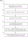
Fig. 2 is a flow diagram of a method for managing reduced power failure energy requirements, according to some embodiments of the invention. The process 200 begins at step 202, where the memory controller 130 receives a plurality of write commands at the host interface 120 of the solid state drive 100 for execution on the solid state drive 100. At step 204, the memory controller 130 stores a plurality of write commands in a cache on the solid state drive 100. For example, the memory controller 130 may store a plurality of write commands in the cache 132 in the volatile memory 130 and may transmit a reply for each write command of the plurality of write commands for execution.
At step 206, the memory controller 130 detects a power failure event on the solid state drive 100. For example, the memory controller 130 may detect a power failure event on the solid state drive 100 by detecting a loss of power from a change in voltage and/or current provided to the solid state drive 100 from the primary power source 170. At step 208, the DC power conditioning and distribution 180 supplies power to the solid state drive 100 from a backup power source (e.g., backup power source 182) on the solid state drive 100 during a power failure event. For example, DC power conditioning and distribution 180 supplies power from a backup power source 182 to the solid state drive 100 during a power failure event.
At step 210, in response to execution, the memory controller 130 removes the one or more write commands from the cache such that the one or more unexecuted write commands remain in the cache. For example, after the corresponding data payload has been written into the non-volatile memory devices 160 a-h, the memory controller 130 removes the one or more executed write commands from the cache 132. The unexecuted write commands remain in cache 132 waiting to be processed. At step 212, the memory controller 130 uses the backup power supply to store the remaining one or more unexecuted write commands, but not its data payload, to the non-volatile memory devices 160 a-h on the solid state drive 100 during the power failure event. For example, the memory controller 130 stores parameters associated with an unexecuted write command to the non-volatile memory devices 160 a-h on the solid state drive 100 before the backup power supply 182 is fully depleted. Thus, when the backup power supply 182 is fully depleted, the data payloads associated with these commands remaining in the cache 132 are lost, but can be reconstructed or recovered from the redundant sources, as previously described.
Other objects, advantages and embodiments of the various aspects of the present invention will be apparent to those skilled in the art and are within the scope of the description and drawings. By way of example, and not limitation, structural or functional elements may be rearranged, or method steps may be reordered, in accordance with the present disclosure. Similarly, a machine may include a single instance or multiple machines, possibly encompassing multiple types of machines that together provide the indicated functionality. The machine types described in various embodiments are not intended to limit the possible machine types that may be used in embodiments of aspects of the invention, and other machines that may accomplish similar tasks may also be implemented. Similarly, principles in accordance with the present invention and methods and systems embodying the same may be applied to other examples which, even if not specifically described herein in detail, would nevertheless be within the scope of the present invention.
Claims (19)
Priority Applications (1)
| Application Number | Priority Date | Filing Date | Title |
|---|---|---|---|
| CN202311659061.4A CN117519450A (en) | 2019-02-13 | 2020-02-05 | Systems and methods for managing reduced power failure energy requirements on solid state drives |
Applications Claiming Priority (3)
| Application Number | Priority Date | Filing Date | Title |
|---|---|---|---|
| US16/274,755 US11048312B2 (en) | 2019-02-13 | 2019-02-13 | Systems and methods for managing reduced power failure energy requirements on a solid state drive |
| US16/274,755 | 2019-02-13 | ||
| PCT/IB2020/000077 WO2020165645A1 (en) | 2019-02-13 | 2020-02-05 | Systems and methods for managing reduced power failure energy requirements on a solid state drive |
Related Child Applications (1)
| Application Number | Title | Priority Date | Filing Date |
|---|---|---|---|
| CN202311659061.4A Division CN117519450A (en) | 2019-02-13 | 2020-02-05 | Systems and methods for managing reduced power failure energy requirements on solid state drives |
Publications (2)
| Publication Number | Publication Date |
|---|---|
| CN113711189A true CN113711189A (en) | 2021-11-26 |
| CN113711189B CN113711189B (en) | 2023-12-26 |
Family
ID=70289821
Family Applications (2)
| Application Number | Title | Priority Date | Filing Date |
|---|---|---|---|
| CN202080026771.1A Active CN113711189B (en) | 2019-02-13 | 2020-02-05 | Systems and methods for managing reduced power failure energy requirements on solid state drives |
| CN202311659061.4A Pending CN117519450A (en) | 2019-02-13 | 2020-02-05 | Systems and methods for managing reduced power failure energy requirements on solid state drives |
Family Applications After (1)
| Application Number | Title | Priority Date | Filing Date |
|---|---|---|---|
| CN202311659061.4A Pending CN117519450A (en) | 2019-02-13 | 2020-02-05 | Systems and methods for managing reduced power failure energy requirements on solid state drives |
Country Status (3)
| Country | Link |
|---|---|
| US (2) | US11048312B2 (en) |
| CN (2) | CN113711189B (en) |
| WO (1) | WO2020165645A1 (en) |
Cited By (1)
| Publication number | Priority date | Publication date | Assignee | Title |
|---|---|---|---|---|
| CN114741037A (en) * | 2022-05-20 | 2022-07-12 | 苏州浪潮智能科技有限公司 | Method, system, terminal and storage medium for reconstructing bitmap structure of disk array |
Families Citing this family (4)
| Publication number | Priority date | Publication date | Assignee | Title |
|---|---|---|---|---|
| WO2019100186A1 (en) * | 2017-11-21 | 2019-05-31 | Intel Corporation | Power management for partial cache line sparing |
| US11221928B2 (en) * | 2019-04-18 | 2022-01-11 | Netapp, Inc. | Methods for cache rewarming in a failover domain and devices thereof |
| US12393244B2 (en) | 2022-12-20 | 2025-08-19 | Samsung Electronics Co., Ltd. | Systems, methods, and apparatus for providing power to storage devices |
| KR20240126300A (en) * | 2023-02-13 | 2024-08-20 | 삼성전자주식회사 | Electronic device resolving sudden power off |
Citations (4)
| Publication number | Priority date | Publication date | Assignee | Title |
|---|---|---|---|---|
| US20140304454A1 (en) * | 2013-04-05 | 2014-10-09 | Sandisk Enterprise Ip Llc | Data hardening in a storage system |
| US20150370700A1 (en) * | 2014-06-23 | 2015-12-24 | Google Inc. | Managing storage devices |
| CN105474192A (en) * | 2013-09-23 | 2016-04-06 | 英特尔公司 | Event-triggered storage of data to non-volatile memory |
| US20170329706A1 (en) * | 2016-05-11 | 2017-11-16 | Seagate Technology Llc | Volatile cache reconstruction after power failure |
Family Cites Families (9)
| Publication number | Priority date | Publication date | Assignee | Title |
|---|---|---|---|---|
| CA2540365C (en) * | 2004-02-05 | 2016-04-05 | Research In Motion Limited | Memory interface controller |
| EP1643506B1 (en) * | 2004-10-04 | 2006-12-06 | Research In Motion Limited | System and method for automatically saving memory contents of a data processing device on power failure |
| JP2012063884A (en) * | 2010-09-14 | 2012-03-29 | Toshiba Corp | Storage device, electronics and control method of storage device |
| US9019067B2 (en) * | 2010-12-30 | 2015-04-28 | Sargent Manufacturing Company | Electronic lock with power failure control circuit |
| US9304901B2 (en) * | 2013-03-14 | 2016-04-05 | Datadirect Networks Inc. | System and method for handling I/O write requests |
| US9372759B2 (en) * | 2014-06-16 | 2016-06-21 | Samsung Electronics Co., Ltd. | Computing system with adaptive back-up mechanism and method of operation thereof |
| US9639287B1 (en) * | 2015-06-29 | 2017-05-02 | Western Digital Technologies, Inc. | Write command reporting |
| US10474532B1 (en) * | 2017-07-28 | 2019-11-12 | EMC IP Holding Company LLC | Automatic fault tolerance in a computing system providing concurrent access to shared computing resource objects |
| US20190243578A1 (en) * | 2018-02-08 | 2019-08-08 | Toshiba Memory Corporation | Memory buffer management for solid state drives |
-
2019
- 2019-02-13 US US16/274,755 patent/US11048312B2/en active Active
-
2020
- 2020-02-05 CN CN202080026771.1A patent/CN113711189B/en active Active
- 2020-02-05 WO PCT/IB2020/000077 patent/WO2020165645A1/en not_active Ceased
- 2020-02-05 CN CN202311659061.4A patent/CN117519450A/en active Pending
-
2021
- 2021-06-22 US US17/354,678 patent/US11803222B2/en active Active
Patent Citations (6)
| Publication number | Priority date | Publication date | Assignee | Title |
|---|---|---|---|---|
| US20140304454A1 (en) * | 2013-04-05 | 2014-10-09 | Sandisk Enterprise Ip Llc | Data hardening in a storage system |
| CN105103140A (en) * | 2013-04-05 | 2015-11-25 | 桑迪士克企业知识产权有限责任公司 | Data hardening in storage systems |
| CN105474192A (en) * | 2013-09-23 | 2016-04-06 | 英特尔公司 | Event-triggered storage of data to non-volatile memory |
| US20150370700A1 (en) * | 2014-06-23 | 2015-12-24 | Google Inc. | Managing storage devices |
| CN106575271A (en) * | 2014-06-23 | 2017-04-19 | 谷歌公司 | Managing storage devices |
| US20170329706A1 (en) * | 2016-05-11 | 2017-11-16 | Seagate Technology Llc | Volatile cache reconstruction after power failure |
Cited By (1)
| Publication number | Priority date | Publication date | Assignee | Title |
|---|---|---|---|---|
| CN114741037A (en) * | 2022-05-20 | 2022-07-12 | 苏州浪潮智能科技有限公司 | Method, system, terminal and storage medium for reconstructing bitmap structure of disk array |
Also Published As
| Publication number | Publication date |
|---|---|
| US11803222B2 (en) | 2023-10-31 |
| US20210318739A1 (en) | 2021-10-14 |
| WO2020165645A1 (en) | 2020-08-20 |
| US20200257346A1 (en) | 2020-08-13 |
| CN113711189B (en) | 2023-12-26 |
| US11048312B2 (en) | 2021-06-29 |
| CN117519450A (en) | 2024-02-06 |
Similar Documents
| Publication | Publication Date | Title |
|---|---|---|
| CN113711189B (en) | Systems and methods for managing reduced power failure energy requirements on solid state drives | |
| US7441081B2 (en) | Write-back caching for disk drives | |
| US8862808B2 (en) | Control apparatus and control method | |
| US10776153B2 (en) | Information processing device and system capable of preventing loss of user data | |
| US10289408B2 (en) | Managing wear of system areas of storage devices | |
| US9158700B2 (en) | Storing cached data in over-provisioned memory in response to power loss | |
| US9075733B1 (en) | Selective storage of address mapping metadata in a system having multiple memories | |
| US8489806B2 (en) | Storage apparatus and method of managing data storage area | |
| US10824344B2 (en) | Solid-state drive with non-volatile random access memory | |
| US20150331624A1 (en) | Host-controlled flash translation layer snapshot | |
| US8909855B2 (en) | Storage system employing MRAM and physically addressed solid state disk | |
| US20190324859A1 (en) | Method and Apparatus for Restoring Data after Power Failure for An Open-Channel Solid State Drive | |
| US20130205065A1 (en) | Methods and structure for an improved solid-state drive for use in caching applications | |
| US9696922B2 (en) | Storage system | |
| US20170060436A1 (en) | Technologies for managing a reserved high-performance memory region of a solid state drive | |
| US8411526B2 (en) | Storage device, electronic device, and storage device control method | |
| CN104050056A (en) | File system backup of multi-storage-medium device | |
| KR20230127934A (en) | Persistent memory device with cache coherent interconnect interface | |
| JP7318367B2 (en) | Storage control device and storage control program | |
| US20130179634A1 (en) | Systems and methods for idle time backup of storage system volumes | |
| US20240264750A1 (en) | Atomic Operations Implemented using Memory Services of Data Storage Devices | |
| WO2016006108A1 (en) | Storage and control method therefor | |
| JP2006099802A (en) | Storage controller and cache memory control method | |
| US20140019678A1 (en) | Disk subsystem and method for controlling memory access |
Legal Events
| Date | Code | Title | Description |
|---|---|---|---|
| PB01 | Publication | ||
| PB01 | Publication | ||
| SE01 | Entry into force of request for substantive examination | ||
| SE01 | Entry into force of request for substantive examination | ||
| GR01 | Patent grant | ||
| GR01 | Patent grant |