Detailed Description
Various features will be described below with reference to the drawings. It should be noted that the figures may or may not be drawn to scale and that elements of similar structure or function are represented by like reference numerals throughout the figures. It should be noted that these figures are only for convenience of description of the features. They are not intended as an exhaustive description of the specification or as a limitation on the scope of the claims. Moreover, the illustrated examples need not have all of the aspects or advantages shown. Aspects or advantages described in connection with a particular example are not necessarily limited to that example and may be practiced in any other example, even if not so illustrated, or if not so explicitly described.
Examples herein describe a peripheral I/O device having a hybrid gateway that allows the device to have an I/O domain and a coherent domain. That is, the I/O device can enjoy the benefits of a traditional I/O model, where the I/O device driver manages some of the computing resources in the I/O device, as well as adding other computing resources in the I/O device to the benefits of the same coherent domain used by a processor (e.g., Central Processing Unit (CPU)) in the host computing system. Thus, the computing resources in the coherent domain of the peripheral I/O device may communicate with the host in a manner similar to CPU-to-CPU communication in the host. This means that the computing resources can utilize coherent types of functionality, such as direct communication (without address translation), more efficient memory usage, non-uniform memory access (NUMA) awareness, and so forth. At the same time, computing resources in the I/O domain may benefit from the advantages of a traditional I/O device model that provides efficiencies when large memory transfers (e.g., Direct Memory Access (DMA)) are made between a host and an I/O device.
To support both I/O and coherent domains in the same peripheral I/O device, the device includes a hybrid gateway that mediates between the host and the I/O device. In one embodiment, the hybrid gateway receives data traffic (e.g., PCIe data traffic) from the host and then splits it into I/O data traffic and coherent data traffic. The I/O data traffic is forwarded to the computing resources in the I/O domain, and the coherent data traffic is forwarded to the computing resources in the coherent domain. For example, a peripheral I/O device may include a Programmable Logic (PL) array, where some blocks of PL in the array are assigned to the I/O domain, while the remaining blocks of PL are assigned to the coherent domain.
Furthermore, the allocation of computing resources to the I/O domain and the coherent domain may be dynamic. For example, a system administrator may determine that there are insufficient resources in the I/O domain and reconfigure the peripheral I/O devices such that computing resources previously allocated to the coherent domain are now allocated to the I/O domain. The I/O devices may be reconfigured with the new allocation scheme and the hybrid gateway may support operation of both the I/O domain and the coherent domain.
FIG. 1 is a block diagram of a host 105 coupled to a peripheral I/O device 135 having an I/O domain and a coherent domain, according to an example. The computing system 100 in fig. 1 includes a host 105 communicatively coupled to a peripheral I/O device 135 using a PCIe connection 130. Host 105 may represent a single computer (e.g., a server) or multiple physical computing systems associated with each other. In any case, host 105 includes operating system 110, multiple CPUs 115, and memory 120. The OS 110 may be any OS capable of performing the functions described herein. In one embodiment, OS 110 (or hypervisor or kernel) establishes a cache-coherent, shared-memory, multi-processor paradigm for CPU 115 and memory 120. In one embodiment, CPU 115 and memory 120 are OS managed (or kernel/hypervisor managed) to form a coherent domain that follows the cache coherent, shared memory, multiprocessor paradigm. However, as described above, the conventional I/O model means that the peripheral I/O devices 135 (and all of their computing resources 150) are excluded from the coherent domain established in the host 105. Instead, the host 105 relies on the I/O device drivers 125 stored in its memory 120, which manage the computing resources 150 in the I/O device 135. That is, the peripheral I/O devices 135 are controlled by the I/O device drivers 125 and are accessible through the I/O device drivers 125.
In embodiments herein, a shared-memory multiprocessor paradigm, along with all of the performance advantages, software flexibility, and reduced overhead of that paradigm, may be used for peripheral I/O devices 135. Furthermore, adding the computing resources in I/O devices 135 to the same coherent domain as CPU 115 and memory 120 allows for a common, ISA-independent development environment. As shown in fig. 1, some of the computing resources 150 in the peripheral I/O devices 135 are allocated to a coherent domain 160, which coherent domain 160 is the same coherent domain 160 used by the computing resources (e.g., CPU 115 and memory 120) in the host 105.
While computing resources 150C and 150D are logically allocated to coherent domain 160, computing resources 150A and 150B are allocated to I/O domain 145. Thus, the I/O devices 135 benefit from the allocation of computing resources 150 to the two domains 145, 160. While the I/O domain 145 provides efficiency in large memory transfers between the host 105 and the I/O device 135, the coherent domain 160 provides the performance advantages, software flexibility, and reduced overhead described above. By logically partitioning hardware computing resources 150 (e.g., programmable logic, network on chip (NoC), data processing engines, and/or memory) into I/O domains 145 and coherent domains 160, I/O devices 135 may benefit from both paradigms.
To enable host 105 to send and receive I/O data traffic and coherent data traffic, peripheral I/O device 135 includes hybrid gateway 140 that splits data received over PCIe connection 130 into I/O data traffic and coherent data traffic the I/O data traffic is forwarded to computing resources 150A and 150B in I/O domain 145 and the coherent data traffic is forwarded to computing resources 150C and 150D in coherent domain 160. In one embodiment, hybrid gateway 140 may process I/O data traffic and coherent data traffic in parallel such that computing resources 150 in I/O domain 145 may execute in parallel with computing resources 150 in coherent domain 160. That is, the host 105 may assign tasks to the computing resources 150 in the I/O domain 145 and the coherent domain 160, which may execute those tasks in parallel.
The peripheral I/O devices 135 may be many different types of I/O devices, such as a pluggable card (plugged into an expansion slot of the host 105), a system on a chip (SoC), a Graphics Processing Unit (GPU), a Field Programmable Gate Array (FPGA), and so forth. Thus, while the remaining embodiments discuss I/O devices 135 including programmable logic (e.g., a programmable logic array), the embodiments may be applied to devices that do not have programmable logic but only contain hardened circuitry (which may be software programmable). Further, while embodiments herein discuss partitioning the computing resources 150 into two domains, in other embodiments, the hybrid gateway 140 may be modified to support additional domains or multiple subdomains within the I/O domain 145 and the coherent domain 160.
FIG. 2 is a block diagram of a peripheral I/O device 135 according to an example in which a Programmable Logic (PL) array 205, a memory block 220, and a NoC 230 are logically divided into an I/O domain 145 and a coherent domain 160. In this example, PL array 205 is formed from a plurality of PL blocks 210. These blocks may be individually assigned to the I/O domain 145 or the coherent domain 160. That is, PL blocks 210A and 210B are assigned to I/O domain 145, while PL blocks 210C and 210D are assigned to coherent domain 160. In one embodiment, the set of PL blocks 210 assigned to the I/O domain and the set of PL blocks 210 assigned to the coherent domain are mutually exclusive such that there is no overlap between the blocks (e.g., no PL blocks 210 are assigned to both the I/O domain and the coherent domain).
In one embodiment, the allocation of hardware resources to the I/O domain 145 or the coherent domain 160 does not affect (or indicate) the physical location of the hardware resources in the I/O device 135. For example, blocks 210A and 210C of PL may be assigned to different domains, even though these blocks are adjacent to each other in PL array 205. Thus, while the physical location of hardware resources in the I/O device 135 may be considered when logically allocated to the I/O domain 145 and the coherent domain 160, this is not required.
The I/O device 135 also includes a memory controller 215 assigned to the I/O domain 145 and the coherent domain 160. In one embodiment, due to the physical interconnection between the memory controllers 215 and the corresponding memory blocks 220, assigning one of the memory controllers 215 to either the I/O domain 145 or the coherent domain 160 means that all of the memory blocks 220 connected to the memory controller 215 are also assigned to the same domain. For example, the memory controller 215 may be coupled to a fixed set of memory blocks 220 (which are not coupled to any other memory controller 215). Thus, the memory blocks 220 may be assigned to the same domain as the memory controller 215 to which they are coupled. However, in other embodiments, memory blocks 220 coupled to the same memory controller 215 may be assigned to different domains.
In one embodiment, the NoC includes interface elements that allow hardware elements (e.g., configurable data processing engines, memory blocks 220, PL blocks 210, etc.) in the I/O devices 135 to send and receive data using the NoC 230. In one embodiment, rather than using programmable logic to form the NoC 230, some or all of the components of the NoC are hardened. In any case, the NoC 230 may logically divide between the I/O domain 145 and the coherent domain 160. In one embodiment, rather than assigning different portions of NoC 230 to the two domains, parameters of the NoC are configured to provide different levels of service for data traffic corresponding to I/O domain 145 and coherence domain 160. That is, data traffic of two domains flowing in the NoC 230 may use the same hardware elements (e.g., switches and communication links), but the hardware elements may have different processing manners. For example, NoC 230 may provide different quality of service (QoS), delay, and bandwidth for two different domains. In addition, NoC 230 may also isolate I/O domain 145 traffic from coherent domain 160 traffic for security reasons.
In another embodiment, NoC 230 may prevent computing resources in I/O domain 145 from communicating with computing resources in coherent domain 160. However, in one embodiment, it may be advantageous to allow the computing resources allocated to the I/O domain 145 to communicate with the computing resources allocated to the coherent domain 160. Previously, such communication would have occurred between the I/O device driver 125 and the OS in the host 105. In contrast, inter-domain communication can occur within I/O devices 135 using NoC 230 (if computing resources are far apart in devices 135) or fabric-to-fabric connections in PL array 205 (if two PL blocks 210 assigned to two different domains are close together and need to communicate).
FIG. 3 is a flow diagram of a method 300 for logically partitioning computing resources in a peripheral device into an I/O domain and a coherent domain, according to an example. The method 300 begins at block 305, where a host receives an indication of an amount of computing resources in a peripheral device for an I/O domain. In one embodiment, the host may provide a Graphical User Interface (GUI) for a user that selects an amount of computing resources in a peripheral device to be allocated to an I/O domain. For example, the GUI may include a text box and the user may enter the percentage of blocks of PL or memory controllers/blocks to assign to the I/O domain. In another embodiment, the GUI allows the user to list the specific resources (e.g., 256kB of memory) that should be allocated to the I/O domain.
At block 310, the host receives an indication of an amount of computing resources in the peripheral device for the coherent domain. As described above, the host may display a separate GUI that enables the user to select the percentage or amount of computing resources allocated to the coherent domain. In another embodiment, the host may include a wizard tool that displays a single GUI that enables a user to divide computing resources between the I/O domain and the coherent domain. For example, the GUI may include a slider that allows a user to divide computing resources such as PL blocks, memory controllers, and memory blocks between two domains. The wizard may include another GUI that allows the user to select parameters for the NoC (e.g., allocate its bandwidth to two domains, establish QoS, establish security/isolation, etc.).
At block 315, the host determines whether the I/O device has sufficient resources to satisfy the requests issued at blocks 305 and 310. For example, a user may request that 500MB of memory be allocated to the I/O domain and 600MB of memory be allocated to the coherent domain, but an I/O device may only have 1GB of memory. Alternatively, the user may have requested that more than 50% of the blocks of PL in the PL array be allocated for the I/O domain and the coherent domain. In those cases, method 300 proceeds to block 320, where the host outputs an error to the user. Method 300 may repeat blocks 305 and 310 so the user may select computing resources that satisfy the hardware constraints in the I/O device. The method 300 may further subdivide the resources allocated at each of the blocks 305 and 310. For example, PL blocks 210A and 210B are assigned to the I/O domain 145 at block 305, while PL blocks 210C and 210D are assigned to the coherent domain 160 at block 310.
However, if the allocation provided by the user satisfies the hardware constraints of the I/O device, then the method 300 proceeds to block 325, where the host configures the peripheral device to have an I/O domain and a coherent domain. In one embodiment, the coherent domain is a shared domain having computational resources in the host. For example, the computing resources selected at block 310 form a coherent domain that follows the cache coherent, shared memory multiprocessor paradigm with CPU, memory, and other hardware elements in the host. At the same time, the computing resources indicated by block 305 form an I/O domain. In one embodiment, the computing resources in the host are located in a different domain than the I/O domain, as opposed to the computing resources in the coherent domain. Thus, the host may still rely on the installed device drivers to communicate with the computing resources in the I/O domain (although communication between the coherent domain and the I/O domain is facilitated by using the fabric in the NoC or PL array as described above).
In one embodiment, the host configures the peripheral device by using a bitstream and/or binary code. The bit stream and binary code configure the computing resources in the peripheral device so that these resources can run in two different domains. For example, blocks of PL selected for coherent domains may be interconnected to each other using structures in the PL array while isolated from blocks of PL assigned to I/O domains. Furthermore, the memory controller may only perform read and write requests received from other hardware elements in the same domain. Furthermore, nocs may use data isolation techniques to ensure that I/O data traffic is managed separately from coherent data traffic. That is, the NoC may identify a difference between data traffic of the two domains. Thus, nocs may provide different bandwidth and QoS levels for data traffic.
At block 330, the peripheral device operates in parallel using the I/O domain and the coherent domain. The peripheral device may perform tasks (possibly assigned by the host) in parallel using computing resources in the I/O domain and the coherent domain. In other words, the peripheral device may support two different domains running in parallel. Thus, hosts can assign different tasks to domains that utilize their respective configurations. For example, tasks that require large amounts of data transfer may be allocated to computing resources in the I/O domain, while tasks that benefit from tight integration or communication with computing resources in the host may be allocated to computing resources in the coherent domain of the peripheral device.
At block 335, the host determines whether it has received a request to reconfigure the domains. In this example, the domains in the peripheral are reconfigurable so that the computing resources originally allocated to the I/O domain may be reallocated to the coherent domain and vice versa. For example, after operating a peripheral device, a user (or monitoring software on a host) may determine that computing resources in one domain are much more idle than computing resources in another domain. For example, a host may assign tasks to one domain more frequently than another domain. In response, the user or monitoring software may request that some of the computing resources in the underutilized domain be reallocated to the overutilized domain by repeating method 300. This may improve the overall ability of the peripheral device to perform tasks assigned by the host.
Fig. 4 is a flow diagram of a method 400 for processing I/O data traffic and coherent data traffic using a hybrid gateway in a peripheral device, according to an example. In one embodiment, method 400 describes a technique for operating a hybrid gateway to support multiple domains in a peripheral device that has been established using, for example, method 300 in fig. 3. For clarity, the blocks of method 400 are discussed in parallel in conjunction with fig. 5, where fig. 5 is a block diagram of a hybrid gateway in a peripheral device according to an example.
At block 405, hybrid gateway 140 receives data traffic from host 105, which includes I/O data traffic and coherent data traffic. That is, the hybrid gateway 140 may use the same connection to receive data traffic destined for the I/O domain and the coherent domain. For example, host 105 may be coupled to peripheral I/O device 135 using one or more PCIe connections 130.
At block 410, hybrid gateway 140 separates the I/O data traffic and the coherent data traffic. For example, coherent data traffic may have special header or header values that indicate to hybrid gateway 140 that the corresponding data is part of the coherent domain, while traffic without these header or header values is identified as I/O data traffic. In this example, the I/O data traffic and the coherent data traffic may be sent using the same protocol (e.g., PCIe) but then separated from each other by hybrid gateway 140.
To this end, the hybrid gateway 140 includes one or more hybrid PCI controllers 505 that can receive data from the host 105 and transmit data to the host 105. Each hybrid PCI controller 505 includes a physical layer 510, a link layer 515, an I/O interconnect layer 520, and a coherent interconnect layer 525. In one embodiment, PCI data (whether it contains I/O data traffic or coherent data traffic) is processed by the physical layer 510 and the link layer 515. However, the hybrid PCI controller 505 then splits the data such that I/O data traffic is handled by the I/O interconnect layer 520 and coherent data traffic is handled by the coherent interconnect layer 525. In this manner, the hybrid PCI controller 505 has I/O hardware components that make the controller 505 compatible with the I/O domain and coherent hardware components that make the controller 505 compatible with the coherent domain.
At block 415, hybrid gateway 140 processes the coherent data using coherent processing engine 540. As shown in fig. 5, the coherent interconnect layer 525 is connected to a coherent processing engine 540, the coherent processing engine 540 serving as an intermediary between the hybrid PCI controller 505 and the computing resources in the peripheral I/O devices 135 assigned to the coherent domain. Coherent processing engine 540 may be implemented using any of a number of different protocols that allow computing resources on peripheral I/O devices to be added to a coherent domain that includes computing resources on a host. For example, the coherent processing engine 540 may form the coherence domain using a cache coherent interconnect for accelerators (CCIX). CCIX is a high-performance chip-to-chip interconnect architecture that provides a cache coherence framework for heterogeneous system architectures. CCIX brings kernel management semantics to peripheral devices. Cache coherency may be automatically maintained at any time between the CPU of the host 105 and various other accelerators in the system, which may be provided in any number of peripheral I/O devices.
However, other coherent interconnect protocols, such as Quick Path Interconnect (QPI) or Omni-Path, may be used in addition to CCIX to extend the coherent domain in host 105 to include computing resources in peripheral I/O device 135. That is, coherent processing engine 540 may be customized to support any type of coherent interconnect protocol that facilitates forming a coherent domain that includes computing resources in I/O device 135.
In one embodiment, the components in
coherent processing engine 540 are hardened (e.g., not formed by using programmable logic), which may improve its performance, as the tasks of
engine 540 may not only perform coherent operations for its domains, but may also perform service requests to ensure coherency is maintained in a multiprocessor system. In the embodiment illustrated in fig. 5,
coherent processing engine 540 comprises a bridge 545 coupled to one of hybrid PCI controller 505,
grid 550, and buffer 555, respectively. The bridge may translate from a coherent interconnect protocol (e.g., CCIX, QPI, Omni-Path, etc.) to an ISA-specific interconnect protocol (e.g., x86, ARM, A,
) The data of (1). In other words, bridge 545 manages protocol semantics over the interface and manages memory actions related to coherent actions.
Grid 550 is a multiprocessor interconnect that routes data to an appropriate cache 555 (or bridge 545 when transferring coherent data from computing resources in I/O device 135 to host 105).
At block 420, coherent processing engine 540 transmits coherent data traffic to computing resources in the coherent domain in the I/O device by using ISA-specific interconnect protocols. As described above, bridge 545 converts coherent data traffic from the coherent interconnect protocol to an ISA-specific interconnect protocol, and then forwards from coherent processing engine 540 to PL array 205 in FIG. 5. That is, buffer 555 is coupled to local buffer 560 in PL array 205, and local buffer 560 is in turn coupled to address translation buffer (ATC)565 for translating memory addresses to local memory addresses. Coherent data traffic may then be processed by the PL blocks in array 205 assigned to the coherent domain.
At block 425, the hybrid gateway 140 transmits the I/O data traffic using a non-coherent interconnect protocol, such as the advanced extensible interface (AXI) protocol. To this end, the hybrid PCI controller 505 in the gateway 140 uses the I/O interconnect layer 520 to convert the received I/O data traffic from the PCI protocol to the non-coherent interconnect protocol. The data may then be forwarded to DMA engine 530 for processing by the Pl blocks assigned to the I/O domain. If the data is forwarded to DMA engine 530, engine 530 may use gateway NoC 535 (which is in hybrid gateway 140 and may be separate from NoC 230) to transfer the data to one of memory controllers 215. That is, gateway NoC 535 is communicatively coupled to NoC 230 so that DMA read and write requests may be performed using memory controller 215 and corresponding memory blocks (not shown in fig. 5).
Thus, using the method 400, the hybrid gateway 140 can receive I/O data traffic and coherent data traffic from the host 105, split and process the data traffic using different hardware components, and forward the data to the appropriate computing elements for processing. Furthermore, the process may also work in reverse, where data processed by computing resources in PL, memory, etc. is transmitted to hybrid gateway 140 and then to host 105 using PCIe connection 130.
In one embodiment, data flows from host 105 to hybrid gateway 140, to the interconnect layers (I/O interconnect layer 520 and coherent interconnect layer 525), to PL array 205 (PL blocks assigned to the I/O domain and PL blocks assigned to the coherent domain), and then to memory blocks (memory blocks assigned to the I/O domain and memory blocks assigned to the coherent domain). However, in another embodiment, data flows from host 105 to hybrid gateway 140, to the interconnect layer (I/O and coherent), to the memory blocks (I/O and coherent memory blocks), and then to PL array 205(I/O and coherent PL blocks). In one embodiment, the transfer of data from PL array 205 to memory blocks, or from memory blocks to PL array 205, is through connections between memory controller 215, NoC 230 and PL array 205.
FIG. 6 illustrates a computing system 600 having computing resources logically divided into I/O domains and coherent domains, according to an example. The system 600 includes a SoC 620 that participates as a peripheral in terms of protocol, discovery, and configuration. Meanwhile, hardware elements that are part of the coherent domain 670 are managed in the host 135 by an OS/kernel (not shown) as processor-memory peers of the host 135 processor-memory complex. Programmable logic and nocs in SoC 620 provide on-device communication, traffic flow, and interfaces between I/O domain 675 and coherent domain 670 when performing heterogeneous acceleration functions by using I/O PL640, coherent PL 645, logic 655, and accelerator logic 650.
Further, the system 600 provides flexibility to locate a compute data set, a compute result, or any communication handshake (doorbell, I/O interrupt, DMA descriptor, semaphore, etc.) between the control processor and the heterogeneous device in the I/O domain 675 or the coherent domain 670.
System components, such as CPUs, I/O devices, accelerators, PL components and memory, may perform functions in any domain using the embodiments described herein. Also within system 600, components such as PL elements, NoC configuration and bandwidth, and on-chip memory (e.g., I/O managed memory 660 and coherent memory 665) and host-attached memory 605 may be logically differentiated between I/O domain 675 and coherent domain 670 to accommodate the particular system and/or application requirements of hybrid gateway 140 acting as a common gateway to the servers/hosts of both domains.
The hardware resources in hybrid gateway 140 may be divided into I/O hardware 630 (e.g., I/O interconnect layer 520 and DMA engine 530 in fig. 5) and coherent hardware 635 (e.g., coherent interconnect layer 525 and coherent processing engine 540). Further, the I/O managed memory 660 and the I/O device driver management memory 610 are allocated to the I/O domain 675, while the coherent memory 615 and the host-attached memory 605 and the coherent memory 665 in the SoC 620 are allocated to the coherent domain 670.
One advantage of embodiments herein is that peripheral I/O devices can be controlled and communicate by PLs (rather than I/O device drivers running on the host CPU-memory complex), which are customized to perform control and communication with peripheral devices and offload I/O device drivers running on the host CPU-memory complex. The PL in turn communicates/cooperates with the host CPU-memory complex as a peer through the coherent domain.
Another advantage of embodiments herein is that the coprocessor/accelerator model and all software and performance efficiencies provided by the model can be utilized without requiring heterogeneous devices to contain the same ISA, the same memory peers of a CPU-memory complex. Instead, coherent acceleration and communication with peripheral connections allows the same processor-to-processor shared-memory model, which is also used for CPU-to-device-accelerator communication, using the same processor-to-processor, shared-memory model as a multiprocessor system.
Another advantage of embodiments herein is that they provide an integrated solution with a shared NoC having QoS attributes, QoS controlled shared resources/buffers, and each part that can be divided into I/O peripheral functions and coherent memory accelerator/remembering functions according to user needs.
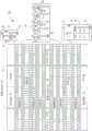
Fig. 7 illustrates an FPGA 700 implementation of I/O peripheral 135, and more particularly with PL array 205 of fig. 2, that includes a number of different programmable blocks, including transceiver 37, CLB 33, BRAM 34, input/output block ("IOB") 36, configuration and clock logic ("CONFIG/CLOCKS") 42, DSP block 35, dedicated input/output block ("IO") 41 (e.g., configuration port and clock port), and other programmable logic 39, such as a digital clock manager, analog-to-digital converter, system monitoring logic, etc. The FPGA may also include a PCIe interface 40, an analog-to-digital converter (ADC)38, and the like.
In some FPGAs, each programmable block may include at least one programmable interconnect element ("INT") 43 having connections to the input and output terminals 48 of the programmable logic elements within the same block, as shown in the example contained at the top of fig. 7. Each programmable interconnect element 43 may also include connections to interconnect segments 49 of adjacent programmable interconnect elements in the same block or other blocks. Each programmable interconnect element 43 may also include connections to interconnect segments 50 of a common routing resource between logic blocks (not shown). The common routing resources may include routing channels between logic blocks (not shown) that include tracks of interconnect segments (e.g., interconnect segment 50) and switch blocks (not shown) for connecting the interconnect segments. An interconnect segment of the generic routing resource (e.g., interconnect segment 50) may span one or more logical blocks. Programmable interconnect elements 43, along with general routing resources, implement a programmable interconnect fabric ("programmable interconnect") for the FPGA shown.
In an example implementation, the CLB 33 may include a configurable logic element ("CLE") 44 that may be programmed to implement user logic, plus a single programmable interconnect element ("INT") 43. BRAM 34 may include a BRAM logic element ("BRL") 45 in addition to one or more programmable interconnect elements. In one embodiment, BRAM 34 is a portion of memory 140 that can retain stored data during reconfiguration as described above. Typically the number of interconnect elements contained in a block depends on the height of the block. In the illustrated example, a BRAM block has the same height as five CLBs, but other numbers (e.g., four) may also be used. In addition to a suitable number of programmable interconnect elements, the DSP block 35 may include a DSP logic element ("DSPL") 46. In addition to one instance of programmable interconnect element 43, IOB 36 may include two instances of an input/output logic element ("IOL") 47, for example. It will be clear to those skilled in the art that the actual IO pads connected to the IO logic elements 47 are generally not limited to the area of the input/output logic elements 47.
In the illustrated example, a horizontal region near the center of the die (as shown in fig. 7) is used for configuration, clock, and other control logic. Vertical columns 51 extending from this horizontal area or column are used to distribute the clock and configuration signals across the width of the FPGA.
Some FPGAs utilizing the architecture shown in fig. 7 include additional logic blocks that disrupt the conventional columnar structure making up a large part of the FPGA. The additional logic blocks may be programmable blocks and/or dedicated logic.
It should be noted that fig. 7 is merely illustrative of an exemplary FPGA architecture. For example, the number of logic blocks in a row, the relative width of the rows, the number and order of rows, the types of logic blocks contained in the rows, the relative sizes of the logic blocks, and the interconnect/logic implementation included at the top of FIG. 7 are purely exemplary. For example, in an actual FPGA, more than one adjacent row of CLBs 102 may be included wherever the CLBs appear, to facilitate efficient implementation of user logic, but the number of adjacent CLB rows varies with the overall size of the FPGA.
In the foregoing, reference is made to the embodiments presented in the present disclosure. However, the scope of the present disclosure is not limited to the specifically described embodiments. Rather, any combination of the described features and elements, whether related to different embodiments or not, is intended to be used in the practice and practice of the intended embodiments. Moreover, although embodiments disclosed herein may achieve advantages over other possible solutions or over the prior art, whether or not a particular advantage is achieved by a given embodiment is not limiting of the scope of the disclosure. Accordingly, the foregoing aspects, features, embodiments and advantages are merely illustrative and are not considered elements or limitations of the appended claims except where explicitly recited in a claim(s).
As will be appreciated by one skilled in the art, the embodiments disclosed herein may be embodied as a system, method or computer program product. Accordingly, aspects may take the form of an entirely hardware embodiment, an entirely software embodiment (including firmware, resident software, micro-code, etc.) or an embodiment combining software and hardware aspects that may all generally be referred to herein as a "circuit," module "or" system. Furthermore, aspects may take the form of a computer program product embodied in one or more computer-readable media having computer-readable program code embodied thereon.
Any combination of one or more computer-readable media may be utilized. The computer readable medium may be a computer readable signal medium or a computer readable storage medium. A computer readable storage medium may be, for example, but not limited to, an electronic, magnetic, optical, electromagnetic, infrared, or semiconductor system, apparatus, or device, or any suitable combination of the foregoing. More specific examples (a non-exhaustive list) of the computer readable storage medium would include the following: an electrical connection having one or more wires, a portable computer diskette, a hard disk, a Random Access Memory (RAM), a read-only memory (ROM), an erasable programmable read-only memory (EPROM or flash memory), an optical fiber, a portable compact disc read-only memory (CD-ROM), an optical storage device, a magnetic storage device, or a suitable combination of any of the foregoing. In the context of this document, a computer readable storage medium is any tangible medium that can contain, or store a program for use by or in connection with an instruction execution system, apparatus, or device.
A computer readable signal medium may include a propagated data signal with computer readable program code embodied therein, for example, in baseband or as part of a carrier wave. Such a propagated signal may take any of a variety of forms, including, but not limited to, electro-magnetic, optical, or any suitable combination thereof. A computer readable signal medium may not be a computer readable storage medium, but may be any computer readable medium that can communicate, propagate, or transport a program for use by or in connection with an instruction execution system, apparatus, or device.
Program code embodied on a computer readable medium may be transmitted using any appropriate medium, including but not limited to wireless, wireline, optical fiber cable, RF, etc., or any suitable combination of the foregoing.
Computer program code for carrying out operations for aspects of the present disclosure may be written in any combination of one or more programming languages, including an object oriented programming language such as Java, Smalltalk, C + + or the like and conventional procedural programming languages, such as the "C" programming language or similar programming languages. The program code may execute entirely on the user's computer, partly on the user's computer, as a stand-alone software package, partly on the user's computer and partly on a remote computer or entirely on the remote computer or server. In the latter scenario, the remote computer may be connected to the user's computer through any type of network, including a Local Area Network (LAN) or a Wide Area Network (WAN), or the connection may be made to an external computer (for example, through the Internet using an Internet service provider).
Aspects of the present disclosure are described below with reference to flowchart illustrations and/or block diagrams of methods, apparatus (systems) and computer program products according to embodiments presented in the disclosure. It will be understood that each block of the flowchart illustrations and/or block diagrams, and combinations of blocks in the flowchart illustrations and/or block diagrams, can be implemented by computer program instructions. These computer program instructions may be provided to a processor of a general purpose computer, special purpose computer, or other programmable data processing apparatus to produce a machine, such that the instructions, which execute via the processor of the computer or other programmable data processing apparatus, create means for implementing the functions/acts specified in the flowchart and/or block diagram block or blocks.
These computer program instructions may also be stored in a computer readable medium that can direct a computer, other programmable data processing apparatus, or other devices to function in a particular manner, such that the instructions stored in the computer readable medium produce an article of manufacture including instructions which implement the function/act specified in the flowchart and/or block diagram block or blocks.
The computer program instructions may also be loaded onto a computer, other programmable data processing apparatus, or other devices to cause a series of operational steps to be performed on the computer, other programmable apparatus or other devices to produce a computer implemented process such that the instructions which execute on the computer or other programmable apparatus provide processes for implementing the functions/acts specified in the flowchart and/or block diagram block or blocks.
The flowchart and block diagrams in the figures illustrate the architecture, functionality, and operation of possible implementations of systems, methods and computer program products according to various examples of the present invention. In this regard, each block in the flowchart or block diagrams may represent a module, segment, or portion of instructions, which comprises one or more executable instructions for implementing the specified logical function(s). In some alternative implementations, the functions noted in the block may occur out of the order noted in the figures. For example, two blocks shown in succession may, in fact, be executed substantially concurrently, or the blocks may sometimes be executed in the reverse order, depending upon the functionality involved. It will also be noted that each block of the block diagrams and/or flowchart illustration, and combinations of blocks in the block diagrams and/or flowchart illustration, can be implemented by special purpose hardware-based systems which perform the specified functions or acts, or combinations of special purpose hardware and computer instructions.
While the foregoing is directed to particular examples, other and further examples may be devised without departing from the basic scope thereof, and the scope thereof is determined by the claims that follow.