CN1136615C - Semiconductor device and method for manufacturing the same - Google Patents
Semiconductor device and method for manufacturing the same Download PDFInfo
- Publication number
- CN1136615C CN1136615C CNB971255245A CN97125524A CN1136615C CN 1136615 C CN1136615 C CN 1136615C CN B971255245 A CNB971255245 A CN B971255245A CN 97125524 A CN97125524 A CN 97125524A CN 1136615 C CN1136615 C CN 1136615C
- Authority
- CN
- China
- Prior art keywords
- insulating film
- protective layer
- capacitor
- interlayer insulating
- semiconductor substrate
- Prior art date
- Legal status (The legal status is an assumption and is not a legal conclusion. Google has not performed a legal analysis and makes no representation as to the accuracy of the status listed.)
- Expired - Fee Related
Links
- 238000000034 method Methods 0.000 title claims abstract description 42
- 238000004519 manufacturing process Methods 0.000 title claims description 71
- 239000004065 semiconductor Substances 0.000 title claims description 42
- 239000003990 capacitor Substances 0.000 claims abstract description 71
- 239000011229 interlayer Substances 0.000 claims abstract description 49
- 239000000758 substrate Substances 0.000 claims abstract description 44
- 238000005530 etching Methods 0.000 claims abstract description 38
- 239000010410 layer Substances 0.000 claims description 78
- 239000011241 protective layer Substances 0.000 claims description 47
- 150000004767 nitrides Chemical group 0.000 claims description 13
- 238000005260 corrosion Methods 0.000 claims description 3
- 230000007797 corrosion Effects 0.000 claims description 3
- 239000002245 particle Substances 0.000 claims description 3
- 230000004888 barrier function Effects 0.000 claims 5
- 238000009413 insulation Methods 0.000 claims 5
- 230000015572 biosynthetic process Effects 0.000 claims 2
- 239000011248 coating agent Substances 0.000 claims 1
- 238000000576 coating method Methods 0.000 claims 1
- 229910021420 polycrystalline silicon Inorganic materials 0.000 description 30
- 229920005591 polysilicon Polymers 0.000 description 30
- 239000005380 borophosphosilicate glass Substances 0.000 description 29
- 238000005229 chemical vapour deposition Methods 0.000 description 26
- 238000000206 photolithography Methods 0.000 description 14
- 229920002120 photoresistant polymer Polymers 0.000 description 14
- 239000007789 gas Substances 0.000 description 9
- 230000003647 oxidation Effects 0.000 description 8
- 238000007254 oxidation reaction Methods 0.000 description 8
- 229910052581 Si3N4 Inorganic materials 0.000 description 5
- 238000010586 diagram Methods 0.000 description 4
- 230000000694 effects Effects 0.000 description 4
- 230000001747 exhibiting effect Effects 0.000 description 4
- 239000000203 mixture Substances 0.000 description 4
- 238000005121 nitriding Methods 0.000 description 4
- ZOXJGFHDIHLPTG-UHFFFAOYSA-N Boron Chemical compound [B] ZOXJGFHDIHLPTG-UHFFFAOYSA-N 0.000 description 3
- OAICVXFJPJFONN-UHFFFAOYSA-N Phosphorus Chemical compound [P] OAICVXFJPJFONN-UHFFFAOYSA-N 0.000 description 3
- 229910052796 boron Inorganic materials 0.000 description 3
- 239000013078 crystal Substances 0.000 description 3
- 238000000059 patterning Methods 0.000 description 3
- 229910052698 phosphorus Inorganic materials 0.000 description 3
- 239000011574 phosphorus Substances 0.000 description 3
- XUIMIQQOPSSXEZ-UHFFFAOYSA-N Silicon Chemical compound [Si] XUIMIQQOPSSXEZ-UHFFFAOYSA-N 0.000 description 2
- 229910021421 monocrystalline silicon Inorganic materials 0.000 description 2
- 229910052710 silicon Inorganic materials 0.000 description 2
- 239000010703 silicon Substances 0.000 description 2
- 239000011521 glass Substances 0.000 description 1
- 239000012528 membrane Substances 0.000 description 1
- 229910044991 metal oxide Inorganic materials 0.000 description 1
- 150000004706 metal oxides Chemical class 0.000 description 1
- 230000000149 penetrating effect Effects 0.000 description 1
- 230000001681 protective effect Effects 0.000 description 1
- 230000003746 surface roughness Effects 0.000 description 1
Images


Classifications
-
- H—ELECTRICITY
- H10—SEMICONDUCTOR DEVICES; ELECTRIC SOLID-STATE DEVICES NOT OTHERWISE PROVIDED FOR
- H10B—ELECTRONIC MEMORY DEVICES
- H10B12/00—Dynamic random access memory [DRAM] devices
- H10B12/30—DRAM devices comprising one-transistor - one-capacitor [1T-1C] memory cells
- H10B12/31—DRAM devices comprising one-transistor - one-capacitor [1T-1C] memory cells having a storage electrode stacked over the transistor
- H10B12/315—DRAM devices comprising one-transistor - one-capacitor [1T-1C] memory cells having a storage electrode stacked over the transistor with the capacitor higher than a bit line
-
- H—ELECTRICITY
- H10—SEMICONDUCTOR DEVICES; ELECTRIC SOLID-STATE DEVICES NOT OTHERWISE PROVIDED FOR
- H10B—ELECTRONIC MEMORY DEVICES
- H10B12/00—Dynamic random access memory [DRAM] devices
- H10B12/01—Manufacture or treatment
- H10B12/02—Manufacture or treatment for one transistor one-capacitor [1T-1C] memory cells
- H10B12/03—Making the capacitor or connections thereto
- H10B12/033—Making the capacitor or connections thereto the capacitor extending over the transistor
-
- H—ELECTRICITY
- H10—SEMICONDUCTOR DEVICES; ELECTRIC SOLID-STATE DEVICES NOT OTHERWISE PROVIDED FOR
- H10D—INORGANIC ELECTRIC SEMICONDUCTOR DEVICES
- H10D1/00—Resistors, capacitors or inductors
- H10D1/01—Manufacture or treatment
- H10D1/041—Manufacture or treatment of capacitors having no potential barriers
- H10D1/042—Manufacture or treatment of capacitors having no potential barriers using deposition processes to form electrode extensions
-
- H—ELECTRICITY
- H10—SEMICONDUCTOR DEVICES; ELECTRIC SOLID-STATE DEVICES NOT OTHERWISE PROVIDED FOR
- H10D—INORGANIC ELECTRIC SEMICONDUCTOR DEVICES
- H10D1/00—Resistors, capacitors or inductors
- H10D1/60—Capacitors
- H10D1/68—Capacitors having no potential barriers
- H10D1/692—Electrodes
- H10D1/711—Electrodes having non-planar surfaces, e.g. formed by texturisation
- H10D1/712—Electrodes having non-planar surfaces, e.g. formed by texturisation being rough surfaces, e.g. using hemispherical grains
-
- H—ELECTRICITY
- H10—SEMICONDUCTOR DEVICES; ELECTRIC SOLID-STATE DEVICES NOT OTHERWISE PROVIDED FOR
- H10D—INORGANIC ELECTRIC SEMICONDUCTOR DEVICES
- H10D1/00—Resistors, capacitors or inductors
- H10D1/60—Capacitors
- H10D1/68—Capacitors having no potential barriers
- H10D1/692—Electrodes
- H10D1/711—Electrodes having non-planar surfaces, e.g. formed by texturisation
- H10D1/716—Electrodes having non-planar surfaces, e.g. formed by texturisation having vertical extensions
-
- H—ELECTRICITY
- H10—SEMICONDUCTOR DEVICES; ELECTRIC SOLID-STATE DEVICES NOT OTHERWISE PROVIDED FOR
- H10D—INORGANIC ELECTRIC SEMICONDUCTOR DEVICES
- H10D84/00—Integrated devices formed in or on semiconductor substrates that comprise only semiconducting layers, e.g. on Si wafers or on GaAs-on-Si wafers
- H10D84/01—Manufacture or treatment
- H10D84/0123—Integrating together multiple components covered by H10D12/00 or H10D30/00, e.g. integrating multiple IGBTs
- H10D84/0126—Integrating together multiple components covered by H10D12/00 or H10D30/00, e.g. integrating multiple IGBTs the components including insulated gates, e.g. IGFETs
- H10D84/0149—Manufacturing their interconnections or electrodes, e.g. source or drain electrodes
-
- H—ELECTRICITY
- H10—SEMICONDUCTOR DEVICES; ELECTRIC SOLID-STATE DEVICES NOT OTHERWISE PROVIDED FOR
- H10B—ELECTRONIC MEMORY DEVICES
- H10B12/00—Dynamic random access memory [DRAM] devices
- H10B12/01—Manufacture or treatment
- H10B12/02—Manufacture or treatment for one transistor one-capacitor [1T-1C] memory cells
- H10B12/03—Making the capacitor or connections thereto
- H10B12/033—Making the capacitor or connections thereto the capacitor extending over the transistor
- H10B12/0335—Making a connection between the transistor and the capacitor, e.g. plug
Landscapes
- Engineering & Computer Science (AREA)
- Manufacturing & Machinery (AREA)
- Semiconductor Memories (AREA)
- Internal Circuitry In Semiconductor Integrated Circuit Devices (AREA)
- Electrodes Of Semiconductors (AREA)
- Semiconductor Integrated Circuits (AREA)
Abstract
Description
本发明一般涉及半导体器件及其制造方法,特别涉及具有关于电容器结构和关于制造该电容器方法的特征的半导体器件及其制造方法。The present invention relates generally to a semiconductor device and a method of manufacturing the same, and more particularly to a semiconductor device and a method of manufacturing the same having features related to the structure of a capacitor and to a method of manufacturing the same.
动态DRAM含有存储信息的电容器。这些电容器在存储器件中排列成矩形,根据外部提供的地址信息在这些电容器中选择位于预定位置的一个电容器。通过写控制系统将信息转换成电荷提供给所选择的电容器。Dynamic DRAM contains capacitors that store information. The capacitors are arranged in a rectangular shape in the memory device, and one capacitor located at a predetermined position is selected among the capacitors based on address information provided from the outside. The information is converted into electrical charges to the selected capacitors by the write control system.
在读的过程中,根据地址信息选择预定位置中的电容器,将被选电容器的电荷读到预先由读控制系统充电的位线。通过读出放大器放大电荷,然后输出到外部。During reading, a capacitor in a predetermined position is selected based on address information, and the charge of the selected capacitor is read to a bit line previously charged by a read control system. The charge is amplified by a sense amplifier and then output to the outside.
图2为DRAM存储单元掩模图形的一个例子,显示了具有常规COB结构的DRAM中的电容器结构。在图2中AC区y1倾斜地形成,位线y2沿X方向延伸,而字线y3沿Y方向延伸。下面结合图3、5和7主要介绍X方向的结构及其制造方法,同时Y方向的结构显示在图4、6和8中。FIG. 2 is an example of a DRAM memory cell mask pattern, showing a capacitor structure in a DRAM having a conventional COB structure. In FIG. 2, the AC region y1 is formed obliquely, the bit line y2 extends in the X direction, and the word line y3 extends in the Y direction. The structure in the X direction and its manufacturing method are mainly introduced below in conjunction with FIGS. 3 , 5 and 7 , while the structure in the Y direction is shown in FIGS. 4 , 6 and 8 .
图3显示的是在制造图2所示的电容器的工艺中的X方向部分。图4显示的是图2中的Y方向部分。在由如Si单晶或类似的半导体组成的衬底51上形成厚度为2000-4000埃数量级的场氧化膜52和厚度约为50-150埃的MOS晶体管(Tr)栅氧化膜53,这两种膜通常通过LOCS(局部硅氧化:选择性氧化)法形成。FIG. 3 shows an X-direction portion in the process of manufacturing the capacitor shown in FIG. 2 . FIG. 4 shows the Y direction part in FIG. 2 . Form a
形成栅氧化膜53和场氧化膜52之后,为电容器提供信号的多个电极54形成在这些膜上。然后,绝缘氧化膜55形成在这些电极54的两侧。由多晶硅或多硅化物(polycide)组成的电极54形成的厚度约为1000-2000埃,通过通常的光刻在Y方向构图并腐蚀。After the gate oxide film 53 and the
形成电极54和氧化膜55后,通过CVD(化学汽相淀积)法在其上形成BPSG(硼磷硅玻璃)膜56。在BPSG膜56上形成贯穿BPSG膜56和栅氧化膜53直达衬底51的孔57。再将电极58连接到通过孔57暴露的衬底51上。通过通常的光刻和腐蚀对由多晶硅或多硅化物组成的电极58进行X方向构图,因而形成电极58。After forming the
此后,如图5所示,通过通常的光刻形成光刻胶图形60,通过腐蚀得到孔61(Y方向部分显示在图6中)。接下来,如图7所示,厚度约为5000-10000埃的多晶硅层62作为电极层形成,用作电容器的一个极板。此后,在电极层62的表面上形成厚度为30-100埃数量级的Si3N膜63,作为电容器的介质层,在Si3N膜63上形成厚度约为1000-2000埃的多晶硅层64,作为电容器的另一个极板。因此完成电容器的制造。图8显示了该电容器的Y方向部分。Thereafter, as shown in FIG. 5, a
然而,在以上介绍的结构中,当减小器件时,DRAM的存储单元触点61的面积不能增大,因此产生为增大电容器的面积使步骤数量增加的问题。另一个问题是存储单元触点的光刻的孔余量很小。However, in the structure described above, when reducing the device, the area of the
本发明的首要目的是设法消除以上提到的问题,提供一种半导体器件及其制造方法,能够增大DRAM的存储单元触点的面积。A primary object of the present invention is to try to eliminate the above-mentioned problems and to provide a semiconductor device and its manufacturing method capable of increasing the contact area of a memory cell of a DRAM.
本发明的另一目的是提供一种半导体器件及其制造方法,能够增大存储单元触点的光刻的孔余量。Another object of the present invention is to provide a semiconductor device and its manufacturing method, which can increase the hole margin of the photolithography of the contact of the memory cell.
根据本发明的半导体器件包括半导体衬底、形成在半导体衬底上并在第一方向内延伸的栅电极、沿栅电极的侧壁在栅电极上形成并显示绝缘特性的第一保护层、形成在包括第一保护层的半导体衬底上的层间绝缘层、具有延伸到第一保护层和半导体衬底的开口部分,在腐蚀工艺中显示出对第一保护层的选择性,还包括开口部分内形成的电容器。A semiconductor device according to the present invention includes a semiconductor substrate, a gate electrode formed on the semiconductor substrate and extending in a first direction, a first protective layer formed on the gate electrode along a side wall of the gate electrode and exhibiting insulating properties, formed An interlayer insulating layer on a semiconductor substrate including a first protective layer, having an opening portion extending to the first protective layer and the semiconductor substrate, exhibiting selectivity to the first protective layer in an etching process, and including the opening part of the capacitor formed within.
第一保护层可以是例如氮化物层,层间绝缘层可以是例如氧化物层。The first protective layer may be, for example, a nitride layer, and the interlayer insulating layer may be, for example, an oxide layer.
此外,电容器可以由连接到半导体衬底并具有粗糙的表面的第一导电层、形成在第一导电层上的电容器绝缘膜、形成在电容器绝缘膜上的第二导电层构成。In addition, the capacitor may be composed of a first conductive layer connected to the semiconductor substrate and having a rough surface, a capacitor insulating film formed on the first conductive layer, and a second conductive layer formed on the capacitor insulating film.
作为选择,层间绝缘层可以由第一绝缘层和形成在第一绝缘层上的第二绝缘层构成。层间绝缘层包含形成在第一绝缘层和第二绝缘层之间的位线,该位线在基本垂直于第一方向的方向内延伸,以及第二保护层,沿位线的侧壁形成在位线上,在腐蚀工艺中显示出对层间绝缘层的选择性及绝缘特性。开口部分延伸到第二保护层。Alternatively, the interlayer insulating layer may be composed of a first insulating layer and a second insulating layer formed on the first insulating layer. The interlayer insulating layer includes a bit line formed between the first insulating layer and the second insulating layer, the bit line extending in a direction substantially perpendicular to the first direction, and a second protective layer formed along a sidewall of the bit line On the bit line, selectivity to the interlayer insulating layer and insulating properties are exhibited in the etching process. The opening portion extends to the second protective layer.
本发明的半导体器件的制造方法可用于制造本发明的半导体器件。The manufacturing method of the semiconductor device of the present invention can be used to manufacture the semiconductor device of the present invention.
该制造方法包括在半导体衬底上形成在第一方向内延伸的栅绝缘膜和栅电极的步骤,在栅电极的上部沿其侧壁形成显示绝缘特性的保护层的步骤,在包括保护层的半导体衬底上形成层间绝缘层的步骤,通过选择性腐蚀层间绝缘层形成延伸到保护层和半导体衬底的开口部分的步骤,和形成开口部分内的电容器的步骤。The manufacturing method includes the steps of forming a gate insulating film and a gate electrode extending in a first direction on a semiconductor substrate, forming a protective layer exhibiting insulating properties on an upper portion of the gate electrode along side walls thereof, and forming a protective layer including the protective layer. A step of forming an interlayer insulating layer on the semiconductor substrate, a step of forming an opening portion extending to the protective layer and the semiconductor substrate by selectively etching the interlayer insulating layer, and a step of forming a capacitor in the opening portion.
在下面结合附图的讨论期间,本发明的其它目的和优点将变得更加明显,其中:Other objects and advantages of the present invention will become more apparent during the following discussion in conjunction with the accompanying drawings, in which:
图1为根据本发明第一实施例的DRAM的基本部分的结构平面图;1 is a structural plan view of an essential part of a DRAM according to a first embodiment of the present invention;
图2为显示现有技术DRAM的结构平面图;FIG. 2 is a structural plan view showing a prior art DRAM;
图3为显示制造现有技术DRAM的步骤剖面图;3 is a sectional view showing steps of manufacturing a prior art DRAM;
图4为显示制造现有技术DRAM的步骤剖面图;4 is a cross-sectional view showing steps of manufacturing a prior art DRAM;
图5为显示制造现有技术DRAM的步骤剖面图;5 is a cross-sectional view showing steps of manufacturing a prior art DRAM;
图6为显示制造现有技术DRAM的步骤剖面图;6 is a sectional view showing steps of manufacturing a prior art DRAM;
图7为显示现有技术DRAM的结构剖面图;7 is a cross-sectional view showing a structure of a prior art DRAM;
图8为显示现有技术DRAM的结构剖面图;8 is a cross-sectional view showing a structure of a prior art DRAM;
图9为显示本发明第一实施例的DRAM的基本部分的结构剖面图;FIG. 9 is a sectional view showing the structure of an essential part of a DRAM according to a first embodiment of the present invention;
图10为显示以上介绍的DRAM的基本部分的结构剖面图;FIG. 10 is a sectional view showing the structure of the essential part of the DRAM introduced above;
图11为显示在本发明第二实施例制造DRAM的方法中制造步骤的剖面图;11 is a sectional view showing manufacturing steps in a method of manufacturing a DRAM according to a second embodiment of the present invention;
图12为显示在制造以上DRAM的方法中制造步骤的剖面图;12 is a sectional view showing manufacturing steps in a method of manufacturing the above DRAM;
图13为显示在制造以上DRAM的方法中制造步骤的剖面图;13 is a sectional view showing manufacturing steps in a method of manufacturing the above DRAM;
图14为显示在制造以上DRAM的方法中制造步骤的剖面图;14 is a sectional view showing manufacturing steps in a method of manufacturing the above DRAM;
图15为显示在制造以上DRAM的方法中制造步骤的剖面图;15 is a sectional view showing manufacturing steps in a method of manufacturing the above DRAM;
图16为显示在制造以上DRAM的方法中制造步骤的剖面图;16 is a sectional view showing manufacturing steps in a method of manufacturing the above DRAM;
图17为显示在制造以上DRAM的方法中制造步骤的剖面图;17 is a sectional view showing manufacturing steps in a method of manufacturing the above DRAM;
图18为显示在制造以上DRAM的方法中制造步骤的剖面图;18 is a sectional view showing manufacturing steps in a method of manufacturing the above DRAM;
图19为显示在制造以上DRAM的方法中制造步骤的剖面图;19 is a sectional view showing manufacturing steps in a method of manufacturing the above DRAM;
图20为显示在制造以上DRAM的方法中制造步骤的剖面图;20 is a sectional view showing manufacturing steps in a method of manufacturing the above DRAM;
图21为显示在制造以上DRAM的方法中制造步骤的剖面图;21 is a sectional view showing manufacturing steps in a method of manufacturing the above DRAM;
图22为显示在制造以上DRAM的方法中制造步骤的剖面图;22 is a sectional view showing manufacturing steps in a method of manufacturing the above DRAM;
图23为根据本发明第三实施例的DRAM的基本部分的结构剖面图;FIG. 23 is a structural sectional view of an essential part of a DRAM according to a third embodiment of the present invention;
图24为显示在本发明第四实施例制造DRAM的方法中制造步骤的剖面图;24 is a sectional view showing manufacturing steps in a method of manufacturing a DRAM according to a fourth embodiment of the present invention;
图25为根据本发明第五实施例的DRAM的基本部分的结构平面图;25 is a structural plan view of an essential part of a DRAM according to a fifth embodiment of the present invention;
图26为以上DRAM的基本部分的结构剖面图;Fig. 26 is a structural sectional view of the basic part of the above DRAM;
图27为DRAM的基本部分的结构剖面图;Fig. 27 is a structural cross-sectional view of a basic part of a DRAM;
图28为显示在本发明第六实施例制造DRAM的方法中制造步骤的剖面图;28 is a cross-sectional view showing manufacturing steps in a method of manufacturing a DRAM according to a sixth embodiment of the present invention;
图29为制造以上DRAM的方法中制造步骤的剖面图;29 is a sectional view of a manufacturing step in a method of manufacturing the above DRAM;
图30为制造以上DRAM的方法中制造步骤的剖面图;30 is a cross-sectional view of a manufacturing step in a method for manufacturing the above DRAM;
图31为制造以上DRAM的方法中制造步骤的剖面图;31 is a cross-sectional view of a manufacturing step in a method for manufacturing the above DRAM;
图32为制造以上DRAM的方法中制造步骤的剖面图;32 is a sectional view of a manufacturing step in a method for manufacturing the above DRAM;
图33为制造以上DRAM的方法中制造步骤的剖面图;33 is a cross-sectional view of a manufacturing step in a method for manufacturing the above DRAM;
图34为制造以上DRAM的方法中制造步骤的剖面图;34 is a sectional view of a manufacturing step in a method for manufacturing the above DRAM;
图35为根据本发明第七实施例的DRAM的基本部分的结构剖面图;35 is a structural sectional view of an essential part of a DRAM according to a seventh embodiment of the present invention;
图36为根据本发明第八实施例制造DRAM的方法中制造步骤的剖面图;36 is a cross-sectional view of manufacturing steps in a method of manufacturing a DRAM according to an eighth embodiment of the present invention;
(第一实施例)(first embodiment)
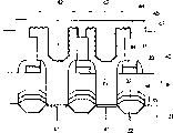
图1、9和10图示了根据本发明第一实施例的DRAM的电容器结构。图1为DRAM的俯视图。图9和10分别为X-X部分和Y-Y部分的示意图。1, 9 and 10 illustrate a capacitor structure of a DRAM according to a first embodiment of the present invention. Figure 1 is a top view of a DRAM. 9 and 10 are schematic diagrams of X-X part and Y-Y part, respectively.
在衬底(半导体衬底)1上形成场氧化膜2,该场氧化膜用于将元件和对应于MOS(金属氧化物半导体)晶体管(Tr)的栅的栅氧化膜3隔开。在该栅氧化膜3上形成电极(栅电极)4,在电极4上形成Si3N4膜(保护层)5。此外,形成由电极4的侧表面延伸到Si3N4膜5的侧表面的侧壁6。On a substrate (semiconductor substrate) 1 is formed a
进一步在场氧化膜2、Si3N4膜5和侧壁6上形成的是层间膜(层间绝缘层)7,用于将这些层与其上形成的层隔开。形成的该层间膜7有一个孔8,露出衬底1用于位线接触。再形成连接到孔8露出的衬底1的电极9和将电极9与其上形成的层隔开的层间膜(层间绝缘层)10。注意在图1和9中示出的孔8和电极9在图1的X-X部分上不存在。Further formed on the
然后,形成穿过层间膜10、7的孔(开口)12。露出衬底1未被保护层5、6覆盖的部分的孔11形成在孔12的底部。积累对应于要保持数据的电荷的电容器向内地形成在该孔12中。Then, holes (openings) 12 are formed through the
该电容器包括形成在层间膜10表面上的电极(第一导电层)13,该电极由孔11沿孔12的外围延伸,并连接到孔11露出的衬底1上。电容器也包括形成在该电极13表面上的电容器绝缘膜14,和进一步形成于其上的电极(第二导电层)15。即,孔11作为存储单元触点,用于将衬底1连接到电极13上。The capacitor includes an electrode (first conductive layer) 13 formed on the surface of the
衬底1由单晶硅(Si)组成。通过通常的LOCOS(局部硅氧化:选择性氧化)法形成厚度为2000-4000埃数量级的场氧化膜2。栅氧化膜3厚度约为50-150埃。电极4由多晶硅或多硅化物组成,厚度约为1000-3000埃。和Si3N4膜5一样,侧壁6由Si3N4形成。电极4由厚度约为1000-3000埃的侧壁(Si3N4膜)6和Si3N4膜5覆盖。层间膜7由BPSG(硼磷硅玻璃:加入硼和磷的氧化膜)组成,约为3000-5000埃厚。和电极4一样,电极9由多晶硅或多硅化物组成,宽度约为1000-2000埃。The
和层间膜7一样,层间膜10由BPSG组成,厚度约为3000-5000埃。电极13由厚度小于1/2孔12宽度的多晶硅组成。通过高选择腐蚀速率,相对于Si3N4膜5、6选择性腐蚀层间BPSG膜7、10形成孔11。因此,Si3N4膜5、6留在孔11的底部,孔11的孔径区域小于孔12的上部的孔径区域。这种形成保护层(Si3N4膜5、6)并仅保留未被保护层覆盖的区域的方法称做自对准。Like the
如上所述,根据第一实施例,使用自对准形成存储单元触点可以增大存储单元触点(孔12)的孔径区域,同时保持存储单元触点的下表面(孔11)的小孔径区域。因此,存储单元触点可形成在栅电极上,因而触点(孔12)的侧壁可用做电容器表面区域。因此,单元芯片区域上的电容器表面积比现有技术的更大。在保持电容器的容量的同时,可减少芯片上的占用面积。As described above, according to the first embodiment, the use of self-alignment to form the memory cell contact can increase the aperture area of the memory cell contact (hole 12) while maintaining the small aperture of the lower surface of the memory cell contact (hole 11) area. Accordingly, a memory cell contact can be formed on the gate electrode, so that the sidewall of the contact (hole 12) can be used as a capacitor surface area. Therefore, the surface area of the capacitor on the unit chip area is larger than that of the prior art. While maintaining the capacity of the capacitor, the footprint on the chip can be reduced.
此外,孔12的孔面积变大,因此在光刻中开孔存储单元触点时,通过图形传递在光刻胶层上开孔时,余量增大。In addition, since the hole area of the
(第二实施例)(second embodiment)
本发明的第二实施例是关于具有图1、9和10中所示结构的DRAM的制造方法。图11-22显示了该制造方法的各个步骤。The second embodiment of the present invention relates to a method of manufacturing a DRAM having the structure shown in FIGS. 1, 9 and 10. Figures 11-22 show the various steps of the manufacturing method.
根据该制造方法,开始,厚度约为2000-4000埃的场氧化膜2形成在Si单晶半导体衬底1上。该步骤通常使用LOCOS法。此后,如图11所示,形成厚度约为50-150埃的MOS-Tr的栅氧化膜3。According to this manufacturing method, initially,
接下来,通过CVD(化学汽相淀积)法在场氧化膜2和栅氧化膜3上形成厚度约为1000-3000埃数量级的层X1,该层X1由多晶硅或多硅化物组成,此后将成为电极4。然后,如图12所示,在该层X1上形成厚度约为1000-3000埃的Si3N4层X2,此后层X2将成为Si3N4膜5。Next, form a layer X1 with a thickness of about 1000-3000 angstroms on the
之后,光刻胶层X3形成在层X2上,如图13所示,当进行腐蚀工艺去掉除必要图形以外的光刻胶时,形成如图14所示的电极4和Si3N4膜5。此后,如图15所示,通过CVD法形成以后将为侧壁6的Si3N4层X4,进行腐蚀工艺。在图15中,该腐蚀为显示出高上-下方向性的各向异性腐蚀。随着该腐蚀的进行,如图16的虚线所示,仅在上-下方向均匀地腐蚀Si3N4层X4,残留的Si3N4层X4成为侧壁6。Afterwards, a photoresist layer X3 is formed on the layer X2, as shown in Figure 13, when an etching process is performed to remove the photoresist except for the necessary pattern, an
接下来,如图17所示,通过CVD法形成厚度约为3000-5000埃的BPSG膜7,通过控制流量使表面平坦。此后,如图18所示,在BPSG膜7上形成光刻胶层X5,在孔8要形成的位置X6除去光刻胶。Next, as shown in FIG. 17, a
此后,进行腐蚀工艺形成孔8,通过CVD法进一步形成一层多晶硅或多硅化物。此外,如图19所示,在垂直于层表面的方向即,在平行于衬底1表面的方向进行构图时,形成电极9。随后,通过CVD法在该电极9上形成厚度约为3000-5000埃的BPSG膜10,通过控制流量使表面平坦。Thereafter, an etching process is performed to form
接下来,如图20所示,在该BPSG膜10上形成光刻胶层11,进行选择性腐蚀工艺去掉对应于以后的孔12位置处的光刻胶。在该选择性腐蚀工艺中,相对于氮化膜(Si3N4膜5、6)选择性腐蚀氧化膜(BPSG膜7、10),因此,如图21所示,Si3N4膜5、6留在孔12的底部没有被腐蚀。该腐蚀工艺包括使用混有C4F2、CO、Ar和O2的气体或加入CH2F2和CHF3的气体。注意该气体的组分比根据器件的尺寸(例如孔12的宽度)适当变化。使用以上介绍的气体进行腐蚀工艺相对于氮化膜(Si3N4膜5、6)选择性腐蚀氧化膜(BPSG膜7、10)。Next, as shown in FIG. 20 , a
形成对氮化膜的腐蚀显示出耐久性的保护层,通过控制选择性腐蚀,采用形成孔11的自对准,形成孔12,因而孔11的宽度可以设定小于孔12上部分的宽度。A protective layer exhibiting durability against etching of the nitride film is formed, and the
此外,通过CVD法形成厚度小于孔12宽度1/2的多晶硅电极层,使用光刻法除去不需要的多晶硅,最终形成的电极13显示在图22中。In addition, a polysilicon electrode layer having a thickness less than 1/2 of the width of the
此后,通过热氮化、热氧化或CVD法等,在电极13的表面上形成如氧化膜和氮化膜的绝缘膜(电容器绝缘膜)14,最后通过CVD法等形成包括多晶硅或类似物的电极15。因此完成具有图1、9和10所示结构的DRAM。Thereafter, an insulating film (capacitor insulating film) 14 such as an oxide film and a nitride film is formed on the surface of the
如上所述,根据第二实施例,使用自对准形成存储单元触点,因而可使存储单元触点(孔12)的孔径区域增大,同时保持存储单元触点底面(孔11)的小孔径区域。因此,可在栅电极上形成存储单元触点,从而接触(孔12)的侧壁可用做电容器表面区域。因此,每单位芯片面积上的电容器表面积比现有技术的更大。As described above, according to the second embodiment, the memory cell contact is formed using self-alignment, thereby enabling the aperture area of the memory cell contact (hole 12) to be enlarged while keeping the bottom surface of the memory cell contact (hole 11) small. aperture area. Thus, a memory cell contact can be formed on the gate electrode so that the sidewall of the contact (hole 12) can be used as a capacitor surface area. Consequently, the capacitor surface area per unit chip area is larger than in the prior art.
此外,孔12的孔径区域可以变大,因此在光刻中开孔存储单元触点时,通过图形传递在光刻胶层上开孔时,余量可以增大。In addition, the aperture area of the
注意在以上讨论的第一和第二实施例中,使用BPSG(硼磷硅玻璃:加入硼和磷的氧化膜)作为层间膜7、10,但也可以使用氧化膜。此时,在以上介绍的情况中,通过改变腐蚀使用的气体的组分进行高选择性的腐蚀工艺。Note that in the first and second embodiments discussed above, BPSG (borophosphosilicate glass: boron and phosphorus added oxide film) is used as the
(第三实施例)(third embodiment)
图23为根据本发明第三实施例的DRAM的电容器结构图。图23为图1的X-X部分,即对应于图9的剖面图。在图23中,与图9中相比,相同或对应的元件使用相同的数字表示。此外,除了电极13′、15′的构形,对应于Y-Y的部分与图1相同,因此进行了省略。同样,平面图与图1相同。FIG. 23 is a diagram of a capacitor structure of a DRAM according to a third embodiment of the present invention. FIG. 23 is the X-X part of FIG. 1 , that is, the cross-sectional view corresponding to FIG. 9 . In FIG. 23 , the same or corresponding elements are denoted by the same numerals as compared with those in FIG. 9 . In addition, except for the configuration of the electrodes 13', 15', the parts corresponding to Y-Y are the same as those in FIG. 1 and thus omitted. Again, the floor plan is the same as in Figure 1.
在图1、9和10所示的DRAM中,电容器的电极13为平面。然而,在第三实施例中,如图2 3所示,电极13′为粗糙表面。和图1、9和10所示的电极13一样,电极13′由多晶硅组成,厚度小于1/2的孔12宽度。电容器绝缘膜14′和电极15′也有粗糙表面,与电极13′的粗糙表面相对应。In the DRAM shown in FIGS. 1, 9 and 10, the
第三实施例显示出与以上讨论的第一实施例相同的效果。此外,在第三实施例中的电极13′、15′都具有粗糙表面,因此比表面平坦的电极有更大的表面积。这可进一步增大每单位芯片面积上的电容器表面积。The third embodiment exhibits the same effects as the first embodiment discussed above. Furthermore, the electrodes 13', 15' in the third embodiment both have rough surfaces and thus have a larger surface area than electrodes with flat surfaces. This can further increase the capacitor surface area per unit chip area.
(第四实施例)(fourth embodiment)
本发明的第四实施例涉及具有图22所示构形的DRAM的制造方法。根据该制造方法,采用以上图11-22中相同的工艺步骤开始,因此得到图21中所示的结构。A fourth embodiment of the present invention relates to a method of manufacturing a DRAM having the configuration shown in FIG. 22 . According to this fabrication method, the same process steps as above in FIGS. 11-22 are used to start, thus resulting in the structure shown in FIG. 21 .
接下来,使用CVD法,形成厚度小于1/2的孔12宽度的多晶硅等的电极层。此时,通过通常的CVD法形成平坦的层后,如多晶硅等的颗粒粘附到该层上,从而形成颗粒状的粗糙表面。然后,通过光刻除去不需要的多晶硅,因此,如图24所示,形成具有粗糙表面的电极13′。Next, using a CVD method, an electrode layer of polysilicon or the like having a thickness less than 1/2 the width of the
此后,通过热氮化、热氧化或CVD法等,在电极13′的表面上形成如氧化膜和氮化膜的绝缘膜(电容器绝缘膜)14′,电容器绝缘膜14′的粗糙度对应于电极13′的粗糙度。最后通过CVD法形成包括多晶硅或类似物的电极15,因此完成具有图23所示结构的DRAM。Thereafter, an insulating film (capacitor insulating film) 14' such as an oxide film and a nitride film is formed on the surface of the electrode 13' by thermal nitriding, thermal oxidation, or CVD method, and the roughness of the capacitor insulating film 14' corresponds to The roughness of the electrode 13'. Finally,
第四实施例显示出与以上讨论的第二实施例相同的效果。此外,在第四实施例中的电极13′、15′都具有粗糙表面,因此比表面平坦的电极有更大的表面积。这可进一步增大每单位芯片面积上的电容器表面积。The fourth embodiment exhibits the same effects as the second embodiment discussed above. Furthermore, the electrodes 13', 15' in the fourth embodiment both have rough surfaces and thus have a larger surface area than electrodes with flat surfaces. This can further increase the capacitor surface area per unit chip area.
(第五实施例)(fifth embodiment)
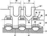
图25-27为根据本发明第五实施例的DRAM的电容器结构图。图25为DRAM的俯视图。图26和27分别显示了X-X部分和Y-Y部分的示意图。25-27 are capacitor structure diagrams of a DRAM according to a fifth embodiment of the present invention. Fig. 25 is a top view of a DRAM. Figures 26 and 27 show schematic views of part X-X and part Y-Y, respectively.
在具有图1、9和10或23所示构形的DRAM中,保护层(Si3N4膜5、6和保护层)仅形成在最底层的电极(栅电极)4上,在自对准的基础上开孔形成存储单元触点(孔11)。然而,根据第五实施例,保护层(Si3N4膜38、39和第二保护层)形成在上层的电极(位线)37上,在自对准的基础上开孔形成存储单元接触(孔41)。In the DRAM having the configuration shown in FIGS. 1, 9 and 10 or 23, the protective layer (Si 3 N 4 films 5, 6 and protective layer) is formed only on the bottommost electrode (gate electrode) On the basis of alignment, holes are opened to form memory cell contacts (holes 11). However, according to the fifth embodiment, the protective layer (Si 3 N 4 films 38, 39 and the second protective layer) is formed on the electrode (bit line) 37 of the upper layer, and the memory cell contact is formed by opening a hole on the basis of self-alignment. (hole 41).
在衬底(半导体衬底)31上形成场氧化膜32,该场氧化膜用于将元件和形成在场氧化膜32上的电极(栅电极)33隔开。在电极33上形成Si3N4膜(第一保护层)34。此外,形成由电极33的侧表面延伸到Si3N4膜34的侧表面的侧壁35。On a substrate (semiconductor substrate) 31 is formed a
进一步在Si3N4膜和侧壁35上形成层间膜(层间绝缘层)36,用于将这些层与其上形成的层隔开。在该层间绝缘膜36上形成的是电极(第二信号线)37、Si3N4膜(第二保护层)38和侧壁39,这与显示在图1、9和10中的电极4、Si3N4膜5和侧壁6具有相同的结构。在Si3N4膜38和侧壁39上再形成层间膜(层间绝缘层)40,用于隔开其上形成的层。注意图25和27中图示的电极37和保护层38,39在图25中的Y-Y部分上不存在。An interlayer film (interlayer insulating layer) 36 is further formed on the Si 3 N 4 film and
然后,形成穿过层间膜40、36的孔(开口)42。露出衬底41未被保护层34、35覆盖的部分的孔41形成在孔42的底部。积累对应于要保持数据的电荷的电容器向内地形成在该孔42中。Then, holes (openings) 42 are formed through the
该电容器包括形成在层间膜36、40表面上的电极(第一导电层)43,该电极由孔41沿孔42的外围延伸,并连接到孔41露出的衬底31。电容器也包括形成在该电极33表面上的电容器绝缘膜44,和进一步形成于其上的电极(第二导电层)45。即,孔41作为存储单元触点,用于将衬底3连接到电极43。The capacitor includes an electrode (first conductive layer) 43 formed on the surface of the
衬底31由单晶硅组成。通过通常的LOCOS法在衬底31上形成厚度为2000-4000埃数量级的场氧化膜32。电极33由多晶硅或多硅化物组成,厚度约为1000-3000埃。和Si3N4膜34一样,侧壁35由Si3N4形成,厚度约为1000-3000埃数量级。The
层间膜36由BPSG组成,厚度约为3000-5000埃。电极37由多晶硅或多硅化物组成,厚度约为1000-2000埃。该电极37被厚度约为1000-3000埃的侧壁Si3N4膜38和Si3N4膜39覆盖。和层间膜36一样,层间膜40由BPSG组成,厚度约为3000-5000埃。电极43由多晶硅等组成,厚度小于1/2的孔12宽度。The
通过高选择腐蚀速率,相对于Si2N4膜38、39选择性腐蚀层间BPSG膜36、40形成孔41。此外,在图27中,该腐蚀显示出高上-下方向性,即在垂直于图25的薄片表面的方向中,如图26所示,用Si3N4膜38、39覆盖的层间膜36未被腐蚀。因此,孔41的孔径区域小于孔42的上部分的孔径区域。 The
如上所述,根据第五实施例,使用自对准形成存储单元触点,可以适当地放大存储单元触点(孔42)的孔径区域,同时保持小的存储单元触点的底面的孔径区域(孔41)。因而在栅电极上形成存储单元触点,通过形成厚度小于存储单元触点的向内1/2孔宽度接触(孔42)的侧壁可用做电容器表面。因此,每单位芯片面积的电容器表面积可设置得比现有技术更大,因此可在保持电容器容量的同时,减小在芯片上所占据的面积。As described above, according to the fifth embodiment, the memory cell contact is formed using self-alignment, and the aperture area of the memory cell contact (hole 42) can be appropriately enlarged while maintaining the small aperture area of the bottom surface of the memory cell contact ( hole 41). Thus forming a memory cell contact on the gate electrode, the sidewall of the contact (hole 42 ) can be used as a capacitor surface by forming an inward 1/2 hole width contact (hole 42 ) with a thickness less than that of the memory cell contact. Therefore, the surface area of the capacitor per unit chip area can be set larger than in the prior art, and thus the area occupied on the chip can be reduced while maintaining the capacity of the capacitor.
此外,孔12的孔面积可以做大,因此在光刻中开孔存储单元触点时,通过图形传递在光刻胶上形成孔时,余量可以增大。In addition, the hole area of the
(第六实施例)(sixth embodiment)
本发明的第六实施例涉及具有图25-27所示构形的DRAM的制造方法。图28-34显示了该制造方法的各个步骤。A sixth embodiment of the present invention relates to a method of manufacturing a DRAM having the configuration shown in FIGS. 25-27. Figures 28-34 show the various steps of the manufacturing method.
根据该制造方法,开始,厚度约为2000-4000埃的场氧化膜32形成在Si单晶半导体衬底31上。该步骤通常使用LOCOS法。此后,如图28所示,形成厚度约为50-150埃的MOS-Tr的栅氧化膜X10。According to this manufacturing method, initially,
接下来,通过CVD(化学汽相淀积)法在场氧化膜32和栅氧化膜x10上形成厚度为1000-3000埃数量级的层X11,该层由多晶硅或多硅化物组成,此后将成为电极33。然后,如图29所示,在该层X11上形成厚度约为1000-3000埃的Si3N4层X12,此后层X12将变为Si3N4膜34。Next, form a layer X11 with a thickness of 1000-3000 angstroms on the
此后,通过进行与图13-16中相同的构图工艺,形成电极33、Si3N4膜34和侧壁35。该工艺后,如图30所示,通过CVD法在其上形成厚度约为3000-5000埃的BPSG膜36,通过控制流量使表面平坦。Thereafter, by performing the same patterning process as in FIGS. 13-16,
在平坦工艺末尾,在BPSG膜36上形成一层多晶硅或多硅化物和Si3N4层。然后,进行以上介绍的相同图形化工艺,如图31所示,形成电极37、Si3N4膜38和侧壁39。At the end of the planarization process, a layer of polysilicon or polysilicide and Si 3 N 4 is formed on the
此后,如图32所示,通过CVD法在其上形成厚度约为3000-5000埃的BPSG膜40,通过控制流量使表面平坦。当平坦工艺结束时,在BPSG膜40上形成光刻胶层X13,除去对应孔42的光刻胶部分。Thereafter, as shown in FIG. 32, a
除去光刻胶后,进行选择性腐蚀。相对于氮化膜(Si3N4膜35,36,38,39),该选择性腐蚀为选择性腐蚀氧化膜(BPSG膜36,40)的工艺。此外,该腐蚀显示出垂直于图33中层表面的高方向性,如图所示,用Si3N4膜38、39覆盖的层间膜36未被腐蚀。该腐蚀工艺涉及使用混有C4F8、CO、Ar、O2的气体,或加入CH2F2、CHF3得到的气体。注意气体的组分比根据器件的尺寸(例如孔12的宽度)适当变化。相对于氮化膜(Si3N4膜5、6)选择性腐蚀氧化膜(BPSG膜7、10)。After removing the photoresist, a selective etch is performed. This selective etching is a process of selectively etching the oxide films (
形成对氮化膜(Si3N4膜38、39)的腐蚀显示出耐久性的保护层,通过进行选择性腐蚀,采用形成孔41的自对准,形成孔42,因而孔41的宽度可以设定小于孔12上部分的宽度。A protective layer showing durability against the corrosion of the nitride film (Si 3 N 4 films 38, 39) is formed, and by performing selective etching, the
此外,通过CVD法形成厚度小于孔12宽度1/2的多晶硅电极层,使用光刻法除去不需要的多晶硅,最终形成的电极43显示在图34中。In addition, a polysilicon electrode layer having a thickness less than 1/2 of the width of the
此后,通过热氮化、热氧化或CVD法等,在电极43的表面上形成如氧化膜和氮化膜的绝缘膜(电容器绝缘膜)44,最后通过CVD法等形成包括多晶硅或类似物的电极45。因此完成具有图25-27所示结构的DRAM。Thereafter, an insulating film (capacitor insulating film) 44 such as an oxide film and a nitride film is formed on the surface of the
如上所述,根据第六实施例,使用自对准形成存储单元触点,因而可使存储单元触点(孔12)的孔径区域增大,同时保持存储单元触点底面(孔11)的小孔径区域。因此,可将栅电极形成于存储单元触点(孔12)内部,从而触点(孔12)的侧壁可用做电容器表面区域。因此,每单位芯片面积上的电容器表面积比现有技术的更大。As described above, according to the sixth embodiment, the memory cell contact is formed using self-alignment, so that the aperture area of the memory cell contact (hole 12) can be enlarged while keeping the bottom surface of the memory cell contact (hole 11) small. aperture area. Therefore, the gate electrode can be formed inside the memory cell contact (hole 12), so that the sidewall of the contact (hole 12) can be used as a capacitor surface area. Consequently, the capacitor surface area per unit chip area is larger than in the prior art.
此外,孔12的孔面积可以做得大,因此在光刻中开孔存储单元触点时,通过图形传递在光刻胶层上开孔时,余量可以增大。In addition, the hole area of the
注意在以上讨论的第五和第六实施例中,使用BPSG(硼磷硅玻璃:加入硼和磷的氧化膜)作为层间膜36、40,但也可以使用氧化膜。此时,在以上介绍的情况中,通过改变腐蚀使用的气体的组分进行高选择性的腐蚀工艺。Note that in the fifth and sixth embodiments discussed above, BPSG (borophosphosilicate glass: oxide film added with boron and phosphorus) is used as the
(第七实施例)(seventh embodiment)
图35为根据本发明第七实施例的DRAM的电容器结构图。图35为图25的X-X部分,即对应于图26的剖面图。在图35中,与图26中相比,相同或对应的元件使用相同的数字表示。此外,除了电极43′、45′的构形,对应于Y-Y的部分与图27相同,因此进行了省略。同样,平面图与图25相同。FIG. 35 is a diagram of a capacitor structure of a DRAM according to a seventh embodiment of the present invention. Fig. 35 is a section X-X of Fig. 25, that is, a sectional view corresponding to Fig. 26 . In FIG. 35 , the same or corresponding elements are denoted by the same numerals as compared with those in FIG. 26 . In addition, except for the configuration of the electrodes 43', 45', the part corresponding to Y-Y is the same as that of FIG. 27, and thus omitted. Also, the plan view is the same as in Fig. 25 .
在图25-27所示的DRAM中,电容器的电极43为平面。然而,在第七实施例中,如图35所示,电极43′为粗糙表面。和图25-27所示的电极43一样,电极43′由多晶硅组成,厚度小于1/2的孔42宽度。电容器绝缘膜44′和电极45′也有粗糙表面,与电极43′的粗糙表面相对应。In the DRAM shown in FIGS. 25-27, the
第七实施例显示出与以上讨论的第五实施例相同的效果。此外,该实施例中的电极43′、45′都具有粗糙表面,因此比表面平坦的电极有更大的表面积。这可进一步增大每单位芯片面积上的电容器表面积。The seventh embodiment exhibits the same effects as the fifth embodiment discussed above. Furthermore, the electrodes 43', 45' in this embodiment both have rough surfaces and thus have a larger surface area than flat-surfaced electrodes. This can further increase the capacitor surface area per unit chip area.
(第八实施例)(eighth embodiment)
本发明的第八实施例涉及具有图35所示构形的DRAM的制造方法。根据该制造方法,采用以上图28-33中相同的工艺步骤开始,因此得到图33中所示的结构。An eighth embodiment of the present invention relates to a method of manufacturing a DRAM having the configuration shown in FIG. 35 . According to this fabrication method, the same process steps as above in FIGS. 28-33 are used to start, thus resulting in the structure shown in FIG. 33 .
接下来,使用CVD法,形成厚度小于1/2的孔12宽度的多晶硅等的电极层。此时,通过通常的CVD法形成平坦的层后,如多晶硅等的颗粒粘附到该层上,从而形成颗粒状的粗糙表面。然后,通过光刻除去不需要的多晶硅,因此,如图36所示,形成具有粗糙表面的电极43′。Next, using a CVD method, an electrode layer of polysilicon or the like having a thickness less than 1/2 the width of the
此后,通过热氮化、热氧化或CVD法等,在电极43的表面上形成如氧化膜和氮化膜的绝缘膜(电容器绝缘膜)44′,电容器绝缘膜44′的粗糙度对应于电极43′表面的粗糙度。最后通过CVD法形成包括多晶硅或类似物的电极45,因此完成具有图35所示结构的电容器。Thereafter, an insulating film (capacitor insulating film) 44' such as an oxide film and a nitride film is formed on the surface of the
第八实施例显示出与以上讨论的第六实施例相同的效果。此外,该实施例中的电极43′、45′都具有粗糙表面,因此比表面平坦的电极有更大的表面积。这可进一步增大每单位芯片面积上的电容器表面积。The eighth embodiment exhibits the same effects as the sixth embodiment discussed above. Furthermore, the electrodes 43', 45' in this embodiment both have rough surfaces and thus have a larger surface area than flat-surfaced electrodes. This can further increase the capacitor surface area per unit chip area.
注意在以上讨论的每个实施例,保护膜由氮化膜形成,中间层由BPSG形成。然而,既使保护层由氧化膜或如BPSG的玻璃形成,通过控制以上介绍的用于腐蚀工艺的气体的混合比例,调节腐蚀的选择比例,从而用以上介绍的相同方式可形成上部分的孔径区域大于暴露的衬底(半导体衬底)的面积的孔。Note that in each of the embodiments discussed above, the protective film is formed of a nitride film, and the intermediate layer is formed of BPSG. However, even if the protective layer is formed of an oxide film or glass such as BPSG, by controlling the mixing ratio of the gases used in the etching process described above, the selective ratio of etching can be adjusted, thereby forming the aperture of the upper part in the same manner as described above. A hole whose area is larger than the area of the exposed substrate (semiconductor substrate).
根据本发明,当形成开口部分时,可设定孔的上部分的区域大于暴露到孔的底部的半导体衬底的区域。形成该孔内电容器,因此可增大DRAM的存储单元触点的面积。此外,由于可增大孔的上部分的面积,可增加光刻中用于存储单元触点的孔径余量。According to the present invention, when forming the opening portion, the area of the upper portion of the hole can be set larger than the area of the semiconductor substrate exposed to the bottom of the hole. Forming this in-hole capacitor increases the contact area of the memory cell of the DRAM. In addition, since the area of the upper portion of the hole can be increased, the aperture margin for the memory cell contact in photolithography can be increased.
显然,在该发明中,在本发明的基础上可形成宽范围的不同的工作模式,但未脱离本发明的精神和范围。本发明不受它的具体的工作模式的限定,而受附带的权利要求的限制。Obviously, in this invention, a wide range of different working modes can be formed on the basis of the present invention without departing from the spirit and scope of the present invention. The invention is not limited by its specific mode of operation, but only by the appended claims.
Claims (7)
Applications Claiming Priority (3)
| Application Number | Priority Date | Filing Date | Title |
|---|---|---|---|
| JP9117956A JPH10308498A (en) | 1997-05-08 | 1997-05-08 | Semiconductor device and manufacturing method thereof |
| JP117956/1997 | 1997-05-08 | ||
| JP117956/97 | 1997-05-08 |
Publications (2)
| Publication Number | Publication Date |
|---|---|
| CN1199247A CN1199247A (en) | 1998-11-18 |
| CN1136615C true CN1136615C (en) | 2004-01-28 |
Family
ID=14724412
Family Applications (1)
| Application Number | Title | Priority Date | Filing Date |
|---|---|---|---|
| CNB971255245A Expired - Fee Related CN1136615C (en) | 1997-05-08 | 1997-12-16 | Semiconductor device and method for manufacturing the same |
Country Status (5)
| Country | Link |
|---|---|
| US (2) | US20020000599A1 (en) |
| JP (1) | JPH10308498A (en) |
| KR (1) | KR100338275B1 (en) |
| CN (1) | CN1136615C (en) |
| TW (1) | TW365016B (en) |
Families Citing this family (10)
| Publication number | Priority date | Publication date | Assignee | Title |
|---|---|---|---|---|
| JP3577195B2 (en) | 1997-05-15 | 2004-10-13 | 株式会社ルネサステクノロジ | Semiconductor device and manufacturing method thereof |
| KR100527592B1 (en) * | 2000-12-12 | 2005-11-09 | 주식회사 하이닉스반도체 | A method for forming a semiconductor device |
| KR100505667B1 (en) * | 2003-01-16 | 2005-08-03 | 삼성전자주식회사 | Method for manufacturing semiconductor device including contact body expanded along bit line direction to contact with storage node |
| KR100497609B1 (en) * | 2003-02-28 | 2005-07-01 | 삼성전자주식회사 | Method of etching silicon nitride film |
| US7288482B2 (en) * | 2005-05-04 | 2007-10-30 | International Business Machines Corporation | Silicon nitride etching methods |
| CN101452905B (en) * | 2007-11-30 | 2012-07-11 | 上海华虹Nec电子有限公司 | Self-alignment contact hole interlayer film, manufacturing method, and contact hole etching method |
| US8369125B2 (en) | 2010-04-16 | 2013-02-05 | SK Hynix Inc. | Semiconductor integrated circuit device capable of securing gate performance and channel length |
| KR20130007375A (en) * | 2011-07-01 | 2013-01-18 | 에스케이하이닉스 주식회사 | Semiconductor device and method for manufacturing the same |
| JP2015211108A (en) * | 2014-04-25 | 2015-11-24 | ルネサスエレクトロニクス株式会社 | Semiconductor device |
| CN114725103B (en) * | 2021-01-05 | 2024-05-17 | 长鑫存储技术有限公司 | Forming method of bit line contact structure and semiconductor structure |
Family Cites Families (10)
| Publication number | Priority date | Publication date | Assignee | Title |
|---|---|---|---|---|
| US5100826A (en) * | 1991-05-03 | 1992-03-31 | Micron Technology, Inc. | Process for manufacturing ultra-dense dynamic random access memories using partially-disposable dielectric filler strips between wordlines |
| US5150276A (en) * | 1992-01-24 | 1992-09-22 | Micron Technology, Inc. | Method of fabricating a vertical parallel cell capacitor having a storage node capacitor plate comprising a center fin effecting electrical communication between itself and parallel annular rings |
| KR960005251B1 (en) * | 1992-10-29 | 1996-04-23 | 삼성전자주식회사 | Manufacturing Method of Semiconductor Memory Device |
| KR940016805A (en) * | 1992-12-31 | 1994-07-25 | 김주용 | Manufacturing method of laminated capacitor of semiconductor device |
| JPH08250677A (en) * | 1994-12-28 | 1996-09-27 | Nippon Steel Corp | Semiconductor memory device and manufacturing method thereof |
| US5658381A (en) * | 1995-05-11 | 1997-08-19 | Micron Technology, Inc. | Method to form hemispherical grain (HSG) silicon by implant seeding followed by vacuum anneal |
| US5940713A (en) * | 1996-03-01 | 1999-08-17 | Micron Technology, Inc. | Method for constructing multiple container capacitor |
| US5789289A (en) * | 1996-06-18 | 1998-08-04 | Vanguard International Semiconductor Corporation | Method for fabricating vertical fin capacitor structures |
| JPH10313102A (en) * | 1997-05-12 | 1998-11-24 | Nec Corp | Semiconductor device and manufacturing method thereof |
| TW417245B (en) * | 1999-07-16 | 2001-01-01 | Taiwan Semiconductor Mfg | Method of producing bitline |
-
1997
- 1997-05-08 JP JP9117956A patent/JPH10308498A/en not_active Withdrawn
- 1997-09-30 US US08/941,065 patent/US20020000599A1/en not_active Abandoned
- 1997-10-28 TW TW086115902A patent/TW365016B/en not_active IP Right Cessation
- 1997-11-27 KR KR1019970063427A patent/KR100338275B1/en not_active IP Right Cessation
- 1997-12-16 CN CNB971255245A patent/CN1136615C/en not_active Expired - Fee Related
-
1999
- 1999-04-12 US US09/289,610 patent/US6383866B1/en not_active Expired - Lifetime
Also Published As
| Publication number | Publication date |
|---|---|
| US20020000599A1 (en) | 2002-01-03 |
| US6383866B1 (en) | 2002-05-07 |
| CN1199247A (en) | 1998-11-18 |
| KR100338275B1 (en) | 2002-08-22 |
| TW365016B (en) | 1999-07-21 |
| KR19980086441A (en) | 1998-12-05 |
| JPH10308498A (en) | 1998-11-17 |
Similar Documents
| Publication | Publication Date | Title |
|---|---|---|
| CN1152433C (en) | Semiconductor device and method for manufacturing thereof | |
| CN1525570A (en) | Semiconductor device and manufacturing method thereof | |
| CN1173394C (en) | Method for manufacturing semiconductor integrated circuit device | |
| CN1767171A (en) | Etch stop structure and manufacture method, and semiconductor device and manufacture method | |
| CN1145208C (en) | Manufacturing method of semiconductor device and semiconductor device | |
| CN1136615C (en) | Semiconductor device and method for manufacturing the same | |
| CN1124407A (en) | Semiconductor integrated circuit device and process for fabricating the same | |
| CN100336199C (en) | Process for producing semiconductor device | |
| CN1512272A (en) | Method for producing semiconductor device using argon fluoride exposure light source | |
| CN1967809A (en) | Method for manufacturing capacitor | |
| CN1623236A (en) | A method of forming a metal pattern and a method of fabricating tft array panel by using the same | |
| CN1240133C (en) | Semiconductor device and its mfg. method | |
| CN1819126A (en) | Method of manufacturing semiconductor device having side wall spacers | |
| CN1797746A (en) | SOI device with different crystallographic orientations | |
| CN1149672C (en) | Semiconductor device and manufacturing method thereof | |
| CN1519914A (en) | Capacitor and its preparation method | |
| CN1276501C (en) | Semiconductor device and method for manufacturing the same | |
| CN1192045A (en) | Manufacturing method of semiconductor device and semiconductor device | |
| CN101047184A (en) | Capacitor structure and manufacturing method thereof | |
| CN1763959A (en) | Semiconductor device and manufacturing method thereof | |
| CN1503329A (en) | Manufacturing method of semiconductor device | |
| CN1440049A (en) | Manufacture for semiconductor devices | |
| CN1129963C (en) | Method of manufacturing semiconductor device | |
| CN1707771A (en) | Method for forming contact plug of semiconductor device | |
| CN1199928A (en) | Semiconductor device and method for manufacturing the same |
Legal Events
| Date | Code | Title | Description |
|---|---|---|---|
| C06 | Publication | ||
| PB01 | Publication | ||
| C10 | Entry into substantive examination | ||
| SE01 | Entry into force of request for substantive examination | ||
| C14 | Grant of patent or utility model | ||
| GR01 | Patent grant | ||
| ASS | Succession or assignment of patent right |
Owner name: OKI SEMICONDUCTOR CO., LTD. Free format text: FORMER OWNER: OKI ELECTRIC INDUSTRY CO., LTD. Effective date: 20090508 |
|
| C41 | Transfer of patent application or patent right or utility model | ||
| TR01 | Transfer of patent right |
Effective date of registration: 20090508 Address after: Tokyo, Japan Patentee after: OKI Semiconductor Co., Ltd. Address before: Tokyo, Japan Patentee before: Oki Electric Industry Co., Ltd. |
|
| C17 | Cessation of patent right | ||
| CF01 | Termination of patent right due to non-payment of annual fee |
Granted publication date: 20040128 Termination date: 20101216 |