CN113543087A - Method and device for determining equipment information - Google Patents
Method and device for determining equipment information Download PDFInfo
- Publication number
- CN113543087A CN113543087A CN202010291993.8A CN202010291993A CN113543087A CN 113543087 A CN113543087 A CN 113543087A CN 202010291993 A CN202010291993 A CN 202010291993A CN 113543087 A CN113543087 A CN 113543087A
- Authority
- CN
- China
- Prior art keywords
- signal
- equipment
- impulse response
- uplink signal
- channel impulse
- Prior art date
- Legal status (The legal status is an assumption and is not a legal conclusion. Google has not performed a legal analysis and makes no representation as to the accuracy of the status listed.)
- Granted
Links
Images


Classifications
-
- H—ELECTRICITY
- H04—ELECTRIC COMMUNICATION TECHNIQUE
- H04W—WIRELESS COMMUNICATION NETWORKS
- H04W4/00—Services specially adapted for wireless communication networks; Facilities therefor
- H04W4/80—Services using short range communication, e.g. near-field communication [NFC], radio-frequency identification [RFID] or low energy communication
-
- G—PHYSICS
- G06—COMPUTING OR CALCULATING; COUNTING
- G06K—GRAPHICAL DATA READING; PRESENTATION OF DATA; RECORD CARRIERS; HANDLING RECORD CARRIERS
- G06K7/00—Methods or arrangements for sensing record carriers, e.g. for reading patterns
- G06K7/10—Methods or arrangements for sensing record carriers, e.g. for reading patterns by electromagnetic radiation, e.g. optical sensing; by corpuscular radiation
- G06K7/10009—Methods or arrangements for sensing record carriers, e.g. for reading patterns by electromagnetic radiation, e.g. optical sensing; by corpuscular radiation sensing by radiation using wavelengths larger than 0.1 mm, e.g. radio-waves or microwaves
- G06K7/10118—Methods or arrangements for sensing record carriers, e.g. for reading patterns by electromagnetic radiation, e.g. optical sensing; by corpuscular radiation sensing by radiation using wavelengths larger than 0.1 mm, e.g. radio-waves or microwaves the sensing being preceded by at least one preliminary step
Landscapes
- Engineering & Computer Science (AREA)
- Toxicology (AREA)
- Physics & Mathematics (AREA)
- Health & Medical Sciences (AREA)
- Artificial Intelligence (AREA)
- General Health & Medical Sciences (AREA)
- Electromagnetism (AREA)
- Computer Vision & Pattern Recognition (AREA)
- General Physics & Mathematics (AREA)
- Theoretical Computer Science (AREA)
- Computer Networks & Wireless Communication (AREA)
- Signal Processing (AREA)
- Mobile Radio Communication Systems (AREA)
Abstract
The application discloses a method and a device for determining equipment information, relates to the technical field of signal processing, and solves the problem that the information efficiency of a tag reader for identifying a plurality of RFID tags in the existing radio frequency identification RFID technology is low. The specific scheme is as follows: for each second device in the plurality of second devices, the first device performs time reversal on the channel impulse response of the second device to obtain a time reversal signal of the second device; the first equipment sends a first downlink signal to the plurality of second equipment according to the time reversal signal of each second equipment; the first device receives a first uplink signal from each second device. And the first equipment determines the equipment information of each second equipment according to the first uplink signal of each second equipment. The method and the device are used for the process that the tag reader identifies the information of the plurality of RFID tags.
Description
Technical Field
The present application relates to the field of signal processing technologies, and in particular, to a method and an apparatus for determining device information.
Background
With the increasing maturity of the internet of things technology, the backscatter communication technology is widely applied, such as a Radio Frequency Identification (RFID) technology. At present, the RFID technology is widely applied to various links of daily life such as library book management, logistics systems, access control systems, food safety tracing and the like.
The RFID technology is implemented as follows: the tag reader transmits a radio frequency signal of a specific frequency, such as a carrier signal, to the electronic device provided with the RFID tag. After receiving the radio frequency signal, the electronic device provided with the RFID tag generates an induced current, enters a working state, triggers the electronic device to modulate information (such as an Identity (ID)) of the RFID tag, and transmits the modulated information of the RFID tag. After receiving the modulated information of the RFID tag, the tag reader transmits the modulated information to a signal processing module of the tag reader, and the signal processing module performs signal processing (such as demodulation and decoding of a signal) and transmits the processed information of the RFID tag to the host. The host machine identifies the information of the RFID label, performs corresponding processing and control aiming at the setting of the information of the RFID label, and sends out a control signal, wherein the control signal is used for controlling the label reader to complete different read-write operations on the information of the RFID label.
In the existing RFID technology, a tag reader can generally acquire information of an RFID tag of only one electronic device at a time and send the information of the RFID tag of the electronic device to a host, that is, the above process is performed once to identify the RFID tag of only one electronic device. When the tag reader needs to acquire information of the RFID tags of the plurality of electronic devices, the tag reader needs to perform the above process for a plurality of times, which reduces the efficiency of identifying the information of the plurality of RFID tags.
Disclosure of Invention
The application provides a method and a device for determining equipment information, and solves the problem that the information efficiency of a tag reader for identifying a plurality of RFID tags in the prior RFID technology is low.
In order to achieve the purpose, the technical scheme is as follows:
in a first aspect, the present application provides a method for determining device information, where the method may be performed by a first device, or may be performed by a determining apparatus supporting the first device to implement the method, where the determining apparatus includes a chip system, and the method includes: for each second device in the plurality of second devices, the first device performs time reversal on the channel impulse response impact of the second device to obtain a time reversal signal of the second device, wherein the time reversal signal is used for focusing the multipath uplink signal of the second device at the first device; the first equipment sends a first downlink signal obtained by superposing the time reversal signal of the second equipment and a plurality of first signals obtained by convolving excitation signals sent by the first equipment to the second equipment to the plurality of second equipment according to the time reversal signal of each second equipment in the plurality of second equipment; the first device receives a first uplink signal from each second device that is a multiplication of the first downlink signal convolved with the channel impulse response of the second device with a backscatter signal indicative of device information of the second device. And the first equipment determines the equipment information of each second equipment according to the first uplink signal of each second equipment.
Based on the method for determining the device information provided by the present application, for each device in the plurality of second devices, the first device performs time reversal on the channel impulse response of the second device to obtain a time reversal signal of the second device, and since the time reversal signal of the second device can focus the multipath uplink signal sent by the second device to the first device at the first device, the first device can send the time reversal signal of each second device in the plurality of second devices to the plurality of second devices, and the time reversal signal is convolved with the excitation signal and then superimposes the first downlink signal, so that the excitation signal sent by the first device to each second device can be focused at the corresponding second device, so that each second device can generate an induced current after receiving the first downlink signal, and enter an operating state to trigger each second device to send the first uplink signal obtained after the device information of the device passes through the channel impulse response of the second device to the first device, that is, the first device may wake up the plurality of second devices to operate by sending a signal to the plurality of second devices once. Because the first uplink signal of each second device received by the first device is obtained by multiplying the first downlink signal after convolving with the channel impulse response of the second device by the backscatter signal of the second device, the backscatter signal of the second device is used for indicating the device information of the second device. In this way, after receiving the first uplink signal from each second device, the first device may determine the device information of each second device according to the first uplink signal of each second device.
Compared with the prior art, in the technical scheme provided in the embodiment of the present application, after the first device may send a signal to the plurality of second devices once, the first device may receive the uplink signal of each of the plurality of second devices, and determine the device information of each of the second devices according to the uplink signal of each of the second devices, so that efficiency of the first device acquiring the device information of the plurality of second devices is improved.
In a possible implementation manner, with reference to the first aspect, the first device sends, to the second device, a second downlink signal for measuring a channel impulse response of the second device; the first device receives a second uplink signal from the second device, the second uplink signal being a second downlink signal reflected back by the second device, and determines a channel impulse response of the second uplink signal. In this way, the first device may determine the first channel impulse response of the second device according to the channel impulse responses of the second downlink signal and the second uplink signal.
Based on the possible implementation manner, the first device may send a probe signal for measuring the channel impulse response of the second device to each second device, so that the first device may determine the channel impulse response of the second device according to the uplink signal reflected back by the second device, which is simple and easy to implement.
In a possible implementation manner, with reference to the first aspect or any one of the possible designs of the first aspect, the first device receives a third uplink signal, which is sent by the excitation source and reflected by the second device, from the second device, and determines a channel impulse response of the third uplink signal. In this way, the first device may determine the first channel impulse response of the second device according to the channel impulse responses of the third downlink signal and the third uplink signal.
Based on the possible implementation, the excitation source sends the second device a detection signal for measuring the channel impulse response of the second device, so that the first device does not need to send a signal to the second device any more, and therefore, the energy consumption of the first device can be reduced.
In a possible implementation manner, with reference to the first aspect or any possible design of the first aspect, after determining a second channel impulse response of a third device other than the second device, the first device determines a channel impulse response of the second device according to a difference between the first channel impulse response and the second channel impulse response.
Based on the possible implementation manner, in order to eliminate the channel impulse response of other interfering devices or interfering paths unrelated to the second device, after determining the channel impulse response of the other devices, the first device subtracts the channel impulse response of the second device from the channel impulse response of the other devices, and the obtained channel impulse response is the channel impulse response of the second device. Therefore, the technical scheme can eliminate the channel impulse response of other interference equipment or interference paths which are not related to the second equipment, so that the channel impulse response of the second equipment can be accurately determined.
In a possible implementation manner, with reference to the first aspect or any possible design of the first aspect, the first device receives an uplink signal that the device other than the second device reflects a downlink signal sent to the second device in a non-signal-reflection state to the first device, and determines a channel impulse response of the device other than the second device according to the uplink signal.
Based on the possible implementation manner, after the downlink signal is sent to the second device in the state of not reflecting the signal, if the first device can also receive an uplink signal that is reflected back by other devices from the downlink signal, the first device may determine that the uplink signal is a signal of the interfering device or the interfering path, and thus the first device may determine the channel impulse response corresponding to the interfering device or the interfering path according to the uplink signal.
In a possible implementation manner, in combination with the first aspect or any one of the possible designs of the first aspect, the excitation signals corresponding to each of the plurality of second devices are orthogonal signals to each other.
Based on the possible implementation manner, when the excitation signals corresponding to each second device are orthogonal signals to each other, since the integral value of the two orthogonal signals within a certain interval is zero, the first device demodulates the first uplink signal of the second device according to the excitation signal of the second device, so that the device information of the second device can be determined.
In a second aspect, the present application further provides a device for determining device information, and for beneficial effects, reference may be made to the description of the first aspect, which is not described herein again. The determining means has the functionality to implement the actions in the method instance of the first aspect described above. The functions can be realized by hardware, and the functions can also be realized by executing corresponding software by hardware. The hardware or software includes one or more modules corresponding to the above-described functions. In one possible design, the determining means includes: a processing unit and a communication unit. The processing unit is used for carrying out time reversal on the channel impulse response impact of the second equipment by the first equipment for each second equipment in the plurality of second equipment to obtain a time reversal signal, used for focusing the multipath uplink signal sent by the second equipment to the first equipment, of the second equipment at the first equipment. And the communication unit is used for sending a plurality of first downlink signals obtained by superposing the time reversal signals of the second equipment and the first signals obtained by convolving the excitation signals sent by the first equipment to the plurality of second equipment according to the time reversal signals of each second equipment, wherein one excitation signal corresponds to one second equipment. And the communication unit is also used for receiving the first uplink signals from the devices of each second device, wherein the first uplink signals are obtained by multiplying the first downlink signals after convolution of the channel impact responses of the second devices and the backscatter signals used for indicating the device information of the second devices. And the processing unit is further used for determining the equipment information of each second equipment according to the first uplink signal of each second equipment.
The units may perform corresponding functions in the method example of the first aspect, for specific reference, detailed description of the method example is given, and details are not repeated here.
In a third aspect, a device information determining apparatus is provided, where the device information determining apparatus may be the first device in the above method embodiment, or a chip disposed in the first device. The determining device comprises a communication interface, a processor and optionally a memory. Wherein the memory is adapted to store a computer program or instructions, and the processor is coupled to the memory and the communication interface, and when the processor executes the computer program or instructions, the determining means is adapted to perform the method performed by the first device in the above-mentioned method embodiments.
In a fourth aspect, there is provided a computer program product comprising: computer program code which, when run, causes the method performed by the first device in the above aspects to be performed.
In a fifth aspect, the present application provides a chip system, which includes a processor, and is configured to implement the functions of the first device in the methods of the above aspects. In one possible design, the system-on-chip further includes a memory for storing program instructions and/or data. The chip system may be formed by a chip, or may include a chip and other discrete devices.
In a seventh aspect, the present application provides a computer-readable storage medium storing a computer program which, when executed, implements the method in the above aspects performed by the first device.
In an eighth aspect, the present application provides a communication system comprising a first device operable to perform the method for determining device information according to the first aspect or any of the possible designs of the first aspect, and a plurality of second devices operable to perform the method for determining device information according to the first aspect or any of the possible designs of the first aspect.
In the present application, the names of the first device, the second device and the determining means do not constitute a limitation on the devices themselves, which may appear under other names in a practical implementation. Provided that the function of each device is similar to that of the present application, and that the devices are within the scope of the claims of the present application and their equivalents.
Drawings
Fig. 1 is a simplified schematic diagram of a communication system based on time reversal provided by the prior art;
FIG. 2 is a simplified schematic diagram of an RFID system provided herein;
fig. 3 is a schematic diagram of a communication system provided herein;
FIG. 4 is a schematic diagram of another communication system provided herein;
FIG. 5 is a schematic diagram of a first apparatus configuration provided herein;
fig. 6 is a flowchart of a method for determining device information provided in the present application;
FIG. 7 is a schematic diagram of an excitation signal provided herein;
fig. 8 is a schematic diagram of a first uplink signal of a second apparatus provided in the present application;
fig. 9a is a flowchart of another method for determining device information provided herein;
fig. 9b is a flowchart of another method for determining device information provided herein;
fig. 10 is a schematic diagram of signal transmission between a first device and a second device provided herein;
fig. 11 is a schematic structural diagram of another first apparatus provided in the present application.
Detailed Description
Before describing the embodiments of the present application, some terms referred to in the embodiments of the present application are explained:
channel impulse response: the channel impulse response is a response signal output at the output terminal of the communication channel after a unit pulse signal passes through the communication channel when the unit pulse signal is input from the input terminal of the communication channel. In a communication system, since a communication channel may affect a passing signal, for example: weakening the energy of the signal, changing the frequency of the signal, etc., different communication channels will affect the signal differently. That is, the channel impulse responses of different communication channels may also be different. Thus, the channel impulse response may be used to represent the fundamental characteristics of the communication channel.
Time Reversal (TR): time reversal can take advantage of the rich multipath radio propagation environment to produce space-time resonance effects, so-called focusing effects, to improve received signal strength while reducing interference.
In one example, as shown in (a) of fig. 1, 3 paths, such as path 1, path 2, and path 3, are included between the receiving end and the transmitting end. The receiving end and the transmitting end can perform signal transmission through a path 1, a path 2 or a path 3.
Referring to fig. 1, the time reversal mainly includes the following three steps:
And 2, the receiving end determines the channel impact response corresponding to each path in a plurality of paths between the receiving end and the sending end, and performs time reversal and conjugation processing on the channel impact response corresponding to each path to obtain a time reversal signal corresponding to each path.
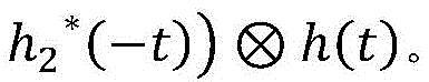
Wherein the time-reversed signal can be used to focus the signal transmitted from the transmitting end to the receiving end at the receiving end. The convolution value of the channel impulse response corresponding to each path and the time reversal signal of the channel impulse response is 1. The convolution value of the channel impulse response corresponding to each path and the time reversal signal of other channel impulse responses is far less than 1.
For example, path 1 corresponds to a channel impulse response of h1(t) path 2 corresponds to a channel impulse response of h2(t)。h1(t) has a time reversal signal of h1 *(-t),h2(t) has a time reversal signal of h2 *(-t). Then

And 3, the receiving end transmits a first transmitting signal to the transmitting end.
The first transmission signal is a signal obtained by convolving and combining a signal to be transmitted and a time reversal signal. The signal to be transmitted is a signal which needs to be transmitted to the transmitting end by the receiving end through a plurality of paths between the receiving end and the transmitting end.
As shown in fig. 1 (b), the receiving end may transmit a first transmission signal to the transmitting end through path 1, path 2, and path 3, respectively.
Wherein the first transmission signal may be gathered at the transmitting end after passing through the path 1, the path 2 and the path 3.
For a scene with a plurality of transmitting terminals, each transmitting terminal transmits a signal to perform channel detection, and a receiving terminal determines that the channel impact response corresponding to each transmitting terminal is hi(t), i ═ 1, 2, …, M. Wherein, M is the number of the sending ends, and M is a positive integer greater than 1. h isiAnd (t) is a channel impulse response corresponding to the ith sending end in the M sending ends. The receiving end carries out time reversal on the channel impact response of each sending end to obtain a time reversal signal h corresponding to the channel impact response of each sending endi *(-t), i ═ 1, 2, …, M. The receiving end respectively convolves and combines a plurality of signals to be transmitted with the time reversal signals to obtain Wherein x iskAnd (t) is a signal sent by the receiving end to the kth sending end. And the receiving end transmits the convolved and combined signals to a plurality of receiving ends, and k is a positive integer less than or equal to M.
For the ith receiving end, the received signal may be:

wherein r isiThe signal received by the ith receiving end is n (t), which is an interference signal.
It should be noted that, the signal received by the ith receiving end is divided into three parts by "+". The first part represents the aggregate signal at the ith receiver of the receiver's transmitted signal to the ith receiver. The second part represents a superimposed signal of the signal transmitted from the receiving end to the other receiving end at the i-th receiving end. The third part is an interference signal. Due to the fact that Much smaller than 1, and therefore the second part can also act as an interference signal. That is, the receiving end may transmit different signals to different transmitting ends through time reversal. For example, the receiving end may transmit
 signal 1 to transmitting end 1 and signal 2 to transmitting end 2.
An RFID system: an RFID system includes an RFID tag and a tag reader.
Wherein the RFID tag: also called electronic tags, smart tags, RFID transponders or RFID data carriers, etc. Typically consisting of a coupling element and a chip, each RFID tag has a unique electronic code. In some scenarios, an RFID tag may be attached to an object for identifying the object.
A tag reader: also known as a reader, a scanner, a reader, a communicator, a reader/writer, or the like. Tag readers are commonly used to read or write information to RFID tags. For example, the tag reader may be a handheld or stationary device.
Fig. 2 shows a schematic diagram of an RFID system provided in an embodiment of the present application. As shown in fig. 2, the RFID system includes a tag reader 110 and an RFID tag 120.
Wherein the tag reader 110 may be provided with at least one antenna that may be used to transmit signals or receive signals. For example, when the tag reader 110 is provided with one antenna, the one antenna can transmit a signal as well as receive a signal. When the tag reader 110 is provided with a plurality of antennas, at least one of the plurality of antennas may be used to transmit signals, and the other antennas except the at least one antenna among the plurality of antennas may be used to receive signals. Without limitation.
In FIG. 2, a tag reader 110 may transmit a radio frequency signal to an electronic device having an RFID tag 120. After receiving the radio frequency signal, the electronic device provided with the RFID tag 120 generates an induced current, enters a working state, triggers the electronic device to modulate the information of the RFID tag 120, and transmits the modulated information of the RFID tag 120 in a form of a modulated signal. After receiving the modulated signal, the tag reader 110 may process the modulated signal to obtain information about the RFID tag.
In the embodiment of the present application, information of the RFID tag may also be referred to as device information. An electronic device may be provided with one or more RFID tags.
In the existing RFID technology, a tag reader can generally acquire information of an RFID tag of only one electronic device at a time and send the information of the RFID tag of the electronic device to a host, that is, the above process is performed once to identify the RFID tag of only one electronic device. When the tag reader needs to acquire information of the RFID tags of the plurality of electronic devices, the tag reader needs to perform the above process for a plurality of times, which reduces the efficiency of identifying the information of the plurality of RFID tags.
In order to solve the above problem, an embodiment of the present application provides a method for determining device information, where the method may include: for each second device in the plurality of second devices, the first device performs time reversal on the channel impulse response of the second device to obtain a time reversal signal, used for focusing the multipath uplink signal sent by the second device to the first device, of the second device at the first device; the first equipment sends first downlink signals to the plurality of second equipment according to the time reversal signals of each second equipment, wherein the first signals are obtained by superposing a plurality of first signals obtained by convolving the time reversal signals of the second equipment with the excitation signals sent by the first equipment; the first device receives a first uplink signal from each second device that is a product of a convolution of the first downlink signal with the channel impulse response of the second device and a backscatter signal carrying device information for the second device. And the first equipment determines the equipment information of each second equipment according to the first uplink signal of each second equipment.
Embodiments of the present application will be described in detail below with reference to the accompanying drawings.
Fig. 3 is a schematic diagram of a communication system to which an embodiment of the present application is applied. As shown in fig. 3, the communication system may include a first device 110, a plurality of second devices 120. The communication system can be applied to the fields of logistics, traffic, identity recognition, anti-counterfeiting, asset management, food, information statistics, transaction, reference application, safety control and the like. For example, the system is applied to book management, logistics management, water, electricity, gas charging, access control management, shelf management, industrial production line management and the like. The application is not limited to a specific application scenario.
The first device may be the tag reader in fig. 2, and is configured to send a downlink signal to the second device 120, for example: probe signals, excitation signals, etc.; and may also be used to receive an upstream signal from the second device, which is a signal from the downstream signal reflected by the second device 120. The first device 110 may be fixed in position or may be mobile.
The second device may have the RFID tag of fig. 2. The information of the RFID tag of each second device may be the same or different, without limitation. The embodiment of the present application does not limit the number of the second devices in the communication system. For example, only 2 second devices 120 (second device 121 and second device 122) are shown in fig. 3.
In fig. 3, a solid line pointing to the second device 120 from the first device 110 indicates that the first device 110 transmits a downlink signal to the second device 120, and a solid line pointing to the first device 110 from the second device 120 indicates that the second device 120 reflects the downlink signal back to the first device 110, that is, a solid line pointing to the first device 110 from the second device 120 indicates that the second device 120 transmits an uplink signal to the first device 110. For example, a solid line 1 represents a downlink signal transmitted from the first device 110 to the second device 121, and a solid line 2 represents the uplink signal transmitted from the second device 121 to the first device 110.
It should be noted that fig. 3 is a schematic diagram, and the communication system may further include other devices, as shown in fig. 4, when the first device 110 does not have to transmit the probe signal to the second device 120, the communication system may further include an excitation source 130, where the excitation source 130 is configured to transmit the probe signal to a plurality of second devices. The stimulus 130 may also be referred to as a stimulus device or have other nomenclature, without limitation. Wherein one detection signal corresponds to one second device.
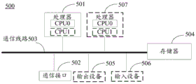
In one specific implementation, each of the devices shown in fig. 3 or 4, such as the first device, may employ the component structure shown in fig. 5 or include the components shown in fig. 5. Fig. 5 is a schematic composition diagram of a device information determining apparatus 500 provided in this embodiment, where when the determining apparatus 500 has the function of the first device described in this embodiment, the determining apparatus 500 may be the first device or a chip or a system on chip in the first device. When the determining apparatus 500 has the functions of the first device described in the embodiments of the present application, the determining apparatus 500 may be a chip or a system on a chip in the first device. As shown in fig. 5, the determining means 500 comprises a processor 501, a communication interface 502 and a communication line 503.
Further, the determining apparatus 500 may further include a memory 504. The processor 501, the memory 504 and the communication interface 502 may be connected by a communication line 503.
The processor 501 is a Central Processing Unit (CPU), a Network Processor (NP), a Digital Signal Processor (DSP), a microprocessor, a microcontroller, a Programmable Logic Device (PLD), or any combination thereof. The processor 501 may also be other devices with processing functions, such as, without limitation, a circuit, a device, or a software module.
A communication interface 502 for communicating with other devices or other communication networks. The other communication network may be an ethernet, a Radio Access Network (RAN), a Wireless Local Area Network (WLAN), or the like. The communication interface 502 may be a module, a circuit, a communication interface, or any device capable of enabling communication.
A communication line 503 for transmitting information between the respective components included in the determination apparatus 500.
A memory 504 for storing instructions. Wherein the instructions may be a computer program.
The memory 504 may be a read-only memory (ROM) or other types of static storage devices that can store static information and/or instructions, a Random Access Memory (RAM) or other types of dynamic storage devices that can store information and/or instructions, an electrically erasable programmable read-only memory (EEPROM), a compact disc read-only memory (CD-ROM) or other optical disc storage, optical disc storage (including compact disc, laser disc, optical disc, digital versatile disc, blu-ray disc, etc.), a magnetic disc storage medium or other magnetic storage devices, and the like, without limitation.
It is to be noted that the memory 504 may exist independently of the processor 501 or may be integrated with the processor 501. The memory 504 may be used for storing instructions or program code or some data etc. The memory 504 may be located inside the determination apparatus 500, or may be located outside the determination apparatus 500, without limitation. The processor 501 is configured to execute the instructions stored in the memory 504 to implement the method for determining device information provided in the following embodiments of the present application.
In one example, processor 501 may include one or more CPUs, such as CPU0 and CPU1 in FIG. 5.
As an alternative implementation, the determining means 500 comprises a plurality of processors, for example, the processor 507 may be included in addition to the processor 501 in fig. 5.
As an alternative implementation, the determining apparatus 500 further includes an output device 505 and an input device 506. Illustratively, the input device 506 is a keyboard, mouse, microphone, or joystick, among other devices, and the output device 505 is a display screen, speaker (spaker), among other devices.
It is noted that the determining apparatus 500 may be a desktop computer, a portable computer, a network server, a mobile phone, a tablet computer, a wireless terminal, an embedded device, a chip system or a device with a similar structure as in fig. 5. Further, the constituent structure shown in fig. 5 does not constitute a limitation of the first device, and the first device may include more or less components than those shown in fig. 5, or combine some components, or a different arrangement of components, in addition to the components shown in fig. 5.
In the embodiment of the present application, the chip system may be composed of a chip, and may also include a chip and other discrete devices.
In addition, acts, terms, and the like referred to between the embodiments of the present application may be mutually referenced and are not limited. In the embodiment of the present application, the name of the message exchanged between the devices or the name of the parameter in the message, etc. are only an example, and other names may also be used in the specific implementation, which is not limited.
The terms "first," "second," and "third," etc. in the description and claims of this application and the above-described drawings are used for distinguishing between different objects and not for limiting a particular order.
In the embodiments of the present application, words such as "exemplary" or "for example" are used to mean serving as an example, instance, or illustration. Any embodiment or design described herein as "exemplary" or "e.g.," is not necessarily to be construed as preferred or advantageous over other embodiments or designs. Rather, use of the word "exemplary" or "such as" is intended to present concepts related in a concrete fashion.
The following describes a method for determining device information provided in an embodiment of the present application with reference to the communication systems shown in fig. 3 and 4. In the embodiment of the present application, the name of the message exchanged between the devices or the name of the parameter in the message, etc. are only an example, and other names may also be used in the specific implementation, which is not limited. The actions related to the embodiments of the present application are only an example, and other names may also be used in the specific implementation, for example: the "carried on" or "included" in the embodiments of the present application may also be replaced by "carried on" or "included" or the like.
Fig. 6 is a flowchart of a method for determining device information according to an embodiment of the present application, and as shown in fig. 6, the method includes:
step 601, for each second device in the plurality of second devices, the first device performs time reversal on the channel impulse response of the second device to obtain a time reversal signal of the second device.
Wherein, the first device may be the first device in fig. 3 or fig. 4, and the second device may be any one of the second devices in fig. 3 or fig. 4.
The channel impulse response of the second device may refer to a response signal of an uplink signal sent by the second device to the first device at the first device, and the detailed description thereof may refer to the above. The determination of the channel impulse response of the second device may be as described with reference to fig. 9a or fig. 9b below.
Wherein the time reversed signal of the second device may be used to focus the multipath uplink signal transmitted by the second device to the first device at the first device. For example, the time reversal of the channel impulse response of the second device by the first device to obtain the time reversal signal of the second device may include: the first equipment sends a detection signal to the second equipment; after receiving the detection signal, the second device may send an uplink signal to the first device through a plurality of paths, where the uplink signal corresponding to each of the plurality of paths is a signal reflected by the detection signal sent by the second device to the second device by the first device; after receiving an uplink signal from the second device, the first device determines a channel impulse response of the uplink signal, that is, a channel impulse response of the second device; and the first equipment performs time reversal on the channel impact response of the second equipment to obtain a time reversal signal of the second equipment.
In a possible implementation manner, in order to reduce energy consumption of the first device, when a distance between the first device and the second device is smaller than a preset length, or the second device moves to a preset detection range of the first device, the first device may be triggered to perform time reversal on a channel impulse response of the second device. Therefore, the first device does not need to send the detection information periodically or in advance, and the energy consumption of the first device is reduced.
The preset length and the preset detection range may be values pre-configured by the first device according to needs, and are not limited.
Step 602, the first device sends a first downlink signal to the plurality of second devices according to the time reversal signal of each of the plurality of second devices.
The first downlink signal may be obtained by adding a plurality of first signals or may be described as a signal obtained by adding a plurality of first signals. The plurality of first signals correspond to the plurality of second devices one to one, that is, one second device corresponds to one first signal. The first signal corresponding to the second device may be obtained by convolving a time-reversed signal of the second device with an excitation signal sent by the first device to the second device. Only one second device is illustrated in fig. 6 as an example, and the description of the plurality of second devices may refer to step 602, which is not repeated.
Wherein one excitation signal corresponds to one second device. The excitation signal may be a carrier signal. For example, as shown in fig. 7, (a) in fig. 7 shows a carrier signal s1(t)=cos(2πf1t), and (b) in fig. 7 shows the carrier type number s2(t)=cos(2πf2t) is shown schematically. Wherein the excitation signal s1(t)=cos(2πf1t) and an excitation signal s2(t)=cos(2πf2t) are all 1. T in FIG. 7 (a)1=1/4f1,t2=3/4f1. T in FIG. 7 (b)3=1/4f2,t4=3/4f2。
For example, the first device may transmit the first downlink signal to the second device through a channel between the first device and the second device.
Take the example of fig. 3 and 4 as an example where the communication system includes 2 second devices. The channel impulse response of the second device 121 is h1(t) the channel impulse response of the second device 122 is h2(t) of (d). The time-reversal signal of the second device 121 is h1 *(-t), the time-reversal signal of the second device 122 is h2 *(-t). The excitation signal sent by the first device to the second device 121 is s1(t), the excitation signal sent by the first device to the second device 122 is s2(t)。
Wherein the first signal corresponding to the second device 121 is The first signal corresponding to the
 second device 122 is
For example, the excitation signal sent by the first device to the second device 121 may be s1(t)=cos(2πf1t), the excitation signal sent by the first device to the second device 122 may be s2(t)=cos(2πf2t). The first downlink signal may be

In order to distinguish the first uplink signal of each second device, the excitation signals corresponding to each second device in the plurality of second devices are orthogonal signals to each other. The two excitation signals are orthogonal to each other, which means that the product of the two excitation signals is 0, e.g. the excitation signal is s1(t) and s2(t) is an example, if s1(t) and s2(t) is orthogonal, then s1(t) and s2(t) the integral over a preset interval is 0, in this way, after the first device receives the first uplink signals of the plurality of second devices, the first device may integrate the first uplink signals, including the excitation signal, of the plurality of second devices respectively by using the excitation signal of the second device, and if the integrated first uplink signals are not eliminated, the first uplink signals are the uplink signals of the second device. And the equipment information of each second equipment is convenient to be determined according to the first uplink signal of each second equipment.
Step 603: the second device receives the first downlink signal from the first device and transmits the first uplink signal to the first device.
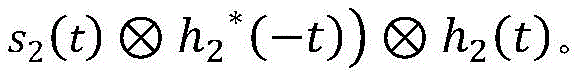
Wherein the second device may receive the first downlink from the first device through a channel between the second device and the first deviceThe first downlink signal received by the second device via the channel between the second device and the first device may be: a convolution between the first downlink signal and a channel impulse response of the second device. For example, the first downlink signal may be
 Wherein the first uplink signal may be
 Where h (t) represents the channel impulse response of the second device.
The first uplink signal may be a product of a first downlink signal transmitted by the first device to the second device and a backscatter signal of the second device.
For example, the sending, by the second device, the first uplink signal to the first device may include:
 wherein b (t) represents the backscatter signal of the second device.
The backscattered signal of the second device may be used to indicate device information of the second device, such as: the backscatter signal of the second device may carry the device information of the second device, or there is a correspondence between the backscatter signal of the second device and the device information of the second device, for example, there is a correspondence shown in table 1 below.
Wherein the first device has a correspondence between the device information of the second device and the backscatter signal of the second device in a case where there is a correspondence between the backscatter signal of the second device and the device information of the second device. The correspondence of the device information of the second device to the backscatter signal of the second device may be presented in the form of a table, i.e. table 1 presents the correspondence. The first device may determine the device information of each second device according to the backscatter signal of each second device and the correspondence.
TABLE 1
| Device information | Backscatter signal |
| Device information of the |
|
| Device information of the |
|
| Device information of the second device 3 | Backscatter signal 3 |
| Device information of the second device 4 | Backscatter signal 4 |
| Device information of the second device 5 | Backscatter signal 5 |
It should be noted that table 1 only shows the storage form of the corresponding relationship in the storage device in a table form, and is not limited to the storage form of the corresponding relationship in the storage device, and of course, the storage form of the corresponding relationship in the storage device may also be stored in other forms, which is not limited in the embodiment of the present application. Table 1 may also include, without limitation, correspondence between device information of other devices and the backscatter signal.
It should be noted that step 603 is described as an example of one second device executing, and it is understood that each of the plurality of second devices needs to execute the process described in step 603.
Step 604, the first device receives the first uplink signal from each second device.
The first uplink signal of one second device is an uplink signal which is reflected by the second device from the first downlink signal received from the first device and includes device information of the second device.
For example, in connection with the example of step 603, the channel impulse response of the second device 121 is h1(t) the channel impulse response of the second device 122 is h2(t) of (d). The backscatter signal of the second device 121 is b1(t) the backscatter signal of the second device 122 is b2(t) of (d). The second device 121 receives the first downlink signal of the first device as
 The first downlink signal of the
 second device 122 received to the first device is
Wherein the first uplink signal of the second device 121 is

The first uplink signal of the second device 122 is

For example, in connection with the example of step 602, the excitation signal s sent by the first device to the second device 1211(t)=cos(2πf1t) and the first device excites the signal s to the second device 1222(t)=cos(2πf2t). First upstream signal s of first device 1211(t)*b1(t)=cos(2πf1t)*b1(t) of (d). First upstream signal s of first device 1222(t)*b2(t)=cos(2πf2t)*b2(t)。
Wherein the multiplication of the excitation signal with the backscatter signal of the second device may result in the amplitude of the excitation signal being reduced but the frequency being kept constant.
For example, the first upstream signal cos (2 π f) of the second device 1211t)*b1(t) the schematic diagram can be shown in FIG. 8 (a), the first uplink signal cos (2 π f) of the second device 1222t)*b2The schematic diagram of (t) may be as shown in (b) of fig. 8. The amplitudes of the first upstream signals of (a) and (b) in fig. 8 are both smaller than 1.
Step 605, the first device determines the device information of each second device according to the first uplink signal of each second device.
For each of the plurality of second devices, the first device may demodulate the first uplink signal of each of the plurality of second devices by using the excitation signal sent by the first device to the second device, and obtain the device information of the second device included in the successfully demodulated first uplink signal of the second device.
For example, the first device may demodulate the excitation signal of the second device 121 with the first uplink signal of each second device, and determine that the first uplink signal, which has the same frequency as the excitation signal of the second device 121, in the successfully demodulated first uplink signals of the plurality of second devices is the first uplink signal of the second device 121.
For example, the first device will excite signal s1(t)=cos(2πf1t) for the first up-going signal cos (2 π f) respectively1t)*b1(t), and a first uplink signal cos (2 π f)2t)*b2(t) demodulating to determine the successfully demodulated first uplink signal cos (2 π f)1t)*b1Frequency and excitation signal s in (t)1(t)=cos(2πf1t) are identical. Thus, the first device may determine the first uplink signal cos (2 π f)1t)*b1(t) is the first upstream signal of the second device 121.
For the method for the second device to demodulate the first uplink signal of each second device by using the excitation signal of the second device, reference may be made to the prior art, and details are not described here.
Based on the method for determining the device information provided by the application, the first device sends the first downlink signal obtained by superimposing the time reversal signal of each second device in the plurality of second devices with the first signal obtained by convolving the excitation signal to the plurality of second devices, so that the excitation signal sent by the first device to each second device can be focused on the corresponding second device, so that each second device can generate an induced current after receiving the first downlink signal and enter a working state, and each second device is triggered to send the device information of the device to the first device in the form of the first uplink signal, that is, the first device can wake up the plurality of second devices to work by sending a signal to the plurality of second devices once. Since the first uplink signal of each second device received by the first device is obtained by multiplying the first downlink signal after convolving with the channel impulse response of the second device by the backscatter signal of the second device, the backscatter signal of the second device can be used to indicate the device information of the second device. In this way, after receiving the first uplink signal from each second device, the first device may determine the device information of each second device according to the first uplink signal of each second device. Compared with the prior art, in the technical scheme provided in the embodiment of the present application, after the first device may send a signal to the plurality of second devices once, the first device may receive the uplink signal of each of the plurality of second devices, and determine the device information of each of the second devices according to the uplink signal of each of the second devices, so that efficiency of the first device acquiring the device information of the plurality of second devices is improved.
For example, the tag reader may transmit a down signal to the device 1 provided with the RFID tag 1 and the device 2 provided with the RFID tag 2. The device 1 provided with the RFID tag 1 returns an uplink signal to the tag reader after receiving the downlink signal, and the device 1 provided with the RFID tag 1 returns an uplink signal to the tag reader after receiving the downlink signal. The tag reader receives an uplink signal of the device 1 provided with the RFID tag 1 and an uplink signal of the device 2 provided with the RFID tag 2, and determines device information of the device 1 according to the uplink signal of the device 1 of the RFID tag 1 and determines device information of the device 2 according to the uplink signal of the device 2 of the RFID tag 2. Therefore, the tag reader can send a signal to the device 1 provided with the RFID tag 1 and the device 2 provided with the RFID tag 2, so that the device information of the device 1 provided with the RFID tag 1 and the device information of the device 2 provided with the RFID tag 2 can be acquired, and the efficiency of identifying the device information of a plurality of devices provided with the RFID tags by the tag reader is improved.
In one possible embodiment, in the method shown in fig. 6, the first device may determine the first channel impulse response of each second device by using the method shown in fig. 9a or the method shown in fig. 9b described below.
The method shown in fig. 9a may include:
step 9011, the first device sends a second downlink signal to the second device. Accordingly, the second device receives a second downlink signal from the first device.
Wherein the first device may be the first device in fig. 3. The second device may be any of the second devices in fig. 3. The second downlink signal is used to measure a channel impulse response of the second device. The second device is in a reflected signal state.
The state that the second device is in the reflected signal state refers to a state that the second device can reflect the downlink signal sent by the first device.
And step 9012, the second device sends a second uplink signal to the first device. Accordingly, the first device receives a second uplink signal from the second device.
The second uplink signal is an uplink signal which is transmitted back by the second downlink signal through the second device.
Step 9013, the first device determines a first channel impulse response of the second device according to the second uplink signal of the second device.
The method shown in fig. 9b may include:
and step 9014, the excitation source sends a third downlink signal to the second device. Accordingly, the second device receives a third downstream signal from the excitation source.
The excitation source may be the excitation source in fig. 4, and the second device may be any one of the second devices in fig. 4. The third downlink signal is used for measuring a channel impulse response of the second device.
And step 9015, the second device sends a third uplink signal to the first device. Accordingly, the first device receives a third uplink signal from the second device.
The third uplink signal is an uplink signal reflected by the second device from the third downlink signal.
Step 9016, the first device determines a first channel impulse response of the second device according to the third uplink signal of the second device.
In a possible embodiment, in order to eliminate an influence of a channel impulse response of another interfering device on a channel impulse response of a second device, the method for determining device information provided in this embodiment may further include: the first device determines a second channel impulse response of the third device. And the first equipment determines the channel impact response of the second equipment according to the difference value of the first channel impact response and the second channel impact response.
Wherein the third device is other interfering devices than the second device. The second channel impulse response is a channel impulse response of the interfering device or the interfering path.
For example, the first channel has an impulse response of hbsc(t) the second channel impulse response is hb(t) of (d). The channel impulse response h of the second device1(t)=hbsc(t)-hb(t)。
In one possible implementation, the first device may determine the second channel impulse response of the third device by the following manner.
The first device or the excitation source sends a fourth downlink signal to the second device in a state of no reflected signal. The first device receives a fourth uplink signal. And the first equipment determines a second channel impact response according to the fourth downlink signal.
The fourth uplink signal is an uplink signal transmitted by the third device to the first device from the fourth downlink signal. The method for determining the second channel impulse response according to the fourth downlink signal by the first device may refer to the method for determining the channel impulse response, which is not described herein again. The second device in the state of not reflecting the signal means that the second device can absorb the downstream signal sent by the first device.
In one example, as shown in fig. 10 (a), after the first device sends a downlink signal to the second device in a state of reflecting a signal, the uplink signal that the first device may receive may be a signal that the second device and the third device reflect the downlink signal sent by the first device back. The first device determines a channel impulse response of the uplink signal, i.e., a first channel impulse response.
In fig. 10 (a), a solid line with double arrows indicates a path through which a downlink signal transmitted from the first device to the second device in the reflected signal state is reflected by the second device in the reflected signal state. The dashed line marked with a single arrow indicates the path along which the downstream signal sent by the first device is reflected back by the third device.
In yet another example, as shown in (b) of fig. 10, when the first device sends a downlink signal to the second device in a state of not reflecting a signal, the uplink signal received by the first device is a signal that is reflected back by the third device from the downlink signal sent by the first device. And the first equipment determines the channel impact response determined by the uplink signal, namely the second channel impact response.
In fig. 10 (b), a solid line with a single-headed arrow indicates a path through which a downlink signal transmitted from the first device to the second device in the state of not reflecting the signal passes, and the downlink signal is absorbed by the second device. The dashed line marked with a single arrow indicates the path along which the downstream signal sent by the first device is reflected back by the third device.
Based on the method for determining the device information provided by the embodiment of the application, after determining the channel impulse responses of other interfering devices, the first device subtracts the channel impulse response of the second device from the channel impulse responses of other interfering devices or interfering paths, and the obtained channel impulse response is the channel impulse response of the second device. Therefore, the technical scheme of the embodiment of the application can eliminate the channel impulse response of other interference devices or interference paths which are not related to the second device, so that the channel impulse response of the second device can be accurately determined.
It is understood that, in order to implement the functions of the above embodiments, the first device includes a corresponding hardware structure and/or software module for performing each function. Those of skill in the art will readily appreciate that the various illustrative elements and method steps described in connection with the embodiments disclosed herein may be implemented as hardware or combinations of hardware and computer software. Whether a function is performed as hardware or computer software driven hardware depends on the particular application scenario and design constraints imposed on the solution.
In the case of an integrated unit, fig. 11 shows a schematic diagram of a possible structure of the device information determining apparatus (denoted as determining apparatus 110) involved in the above embodiments, where the determining apparatus 110 includes a communication unit 111 and a processing unit 112, and may further include a storage unit 113. The schematic configuration shown in fig. 11 may be used to illustrate the configuration of the first device according to the above-described embodiment, or the configuration of the second device according to the above-described embodiment, or the configuration of the excitation source according to the above-described embodiment.
When the schematic configuration diagram shown in fig. 11 is used to illustrate the configuration of the first device in the above-described embodiment, the processing unit 112 is configured to control and manage the actions of the first device, for example, the processing unit 112 is configured to execute step 601 and step 605 in fig. 6, step 9013 in fig. 9a and step 9016 in fig. 9b, execute step 603 in fig. 6 through the communication unit 111, and/or execute the actions performed by the first device in other processes described in this embodiment. The storage unit 113 is used to store program codes and data of the first device.
When the schematic structure diagram shown in fig. 11 is used to illustrate the structure of the first device in the above embodiment, the determining device 110 may be the first device, or may be a chip in the first device.
When the schematic structure shown in fig. 11 is used to illustrate the structure of the second device in the above embodiments, the processing unit 112 is configured to control and manage the actions of the second device, for example, the processing unit 112 executes the actions performed by the first device in step 602 in fig. 6, step 9012 in fig. 9a, step 9115 in fig. 9b, and/or other processes described in this embodiment through the communication unit 111. The storage unit 113 is used to store program codes and data of the first device.
When the schematic structure diagram shown in fig. 11 is used to illustrate the structure of the second device in the above embodiment, the determining device 110 may be the first device or a chip in the second device.
When the schematic structure shown in fig. 11 is used to illustrate the structure of the excitation source in the above embodiment, the processing unit 112 is used to control and manage the actions of the excitation source, for example, the processing unit 112 executes the actions performed by the excitation source in step 9014 in fig. 9b and/or other processes described in this embodiment through the communication unit 111. The memory unit 113 is used to store program codes and data of the stimulus source.
When the schematic configuration shown in fig. 11 is used to illustrate the configuration of the excitation source in the above embodiment, the determination device 110 may be the excitation source or a chip in the excitation source.
Wherein, when the determining means 110 is the first device, the processing unit 112 may be a processor or a controller, and the communication unit 111 may be a communication interface, a transceiver circuit, a transceiver means, etc. The communication interface is a generic term, and may include one or more interfaces. The storage unit 113 may be a memory. When the determining means 110 is a chip within the first device, the processing unit 112 may be a processor or a controller, and the communication unit 111 may be an input interface and/or an output interface, a pin or a circuit, etc. The storage unit 113 may be a storage unit (e.g., a register, a cache, etc.) in the chip, or may be a storage unit (e.g., a read-only memory (ROM), a Random Access Memory (RAM), etc.) in the first device, which is located outside the chip.
Wherein, when the determining apparatus 110 is the second device, the processing unit 112 may be a processor or a controller, and the communication unit 111 may be a communication interface, a transceiver circuit, a transceiver apparatus, and the like. The communication interface is a generic term, and may include one or more interfaces. The storage unit 113 may be a memory. When the determining means 110 is a chip within the second device, the processing unit 112 may be a processor or a controller, and the communication unit 111 may be an input interface and/or an output interface, a pin or a circuit, etc. The storage unit 113 may be a storage unit (e.g., a register, a cache, etc.) in the chip, or may be a storage unit (e.g., a read-only memory (ROM), a Random Access Memory (RAM), etc.) in the second device, which is located outside the chip.
Wherein, when the determining device 110 is the excitation source, the processing unit 112 may be a processor or a controller, and the communication unit 111 may be a communication interface, a transceiver circuit, a transceiver device, etc. The communication interface is a generic term, and may include one or more interfaces. The storage unit 113 may be a memory. When the apparatus 110 is determined to be a chip within the stimulus source, the processing unit 112 may be a processor or a controller, and the communication unit 111 may be an input interface and/or an output interface, pins or circuits, etc. The storage unit 113 may be a storage unit (e.g., a register, a cache, etc.) in the chip, or may be a storage unit (e.g., a read-only memory (ROM), a Random Access Memory (RAM), etc.) located outside the chip in the excitation source.
The communication unit may also be referred to as a transceiver unit. The antenna and the control circuit having a transceiving function in the determination device 110 may be regarded as a communication unit of the determination device, and the processor having a processing function may be regarded as a processing unit of the determination device. Optionally, a device in the communication unit for implementing the receiving function may be regarded as a receiving unit, where the receiving unit is configured to perform the receiving step in the embodiment of the present application, and the receiving unit may be a receiver, a receiving circuit, and the like. The device for realizing the transmission function in the communication unit may be regarded as a transmission unit for performing the steps of transmission in the embodiments of the present application, and the transmission unit may be a transmitter, a transmission circuit, or the like.
The integrated unit in fig. 11, if implemented in the form of a software functional module and sold or used as a separate product, may be stored in a computer-readable storage medium. Based on such understanding, the technical solutions of the embodiments of the present application may be essentially implemented or make a contribution to the prior art, or all or part of the technical solutions may be implemented in the form of a software product stored in a storage medium, and including several instructions for causing a computer device (which may be a personal computer, a server, or a first device, etc.) or a processor (processor) to execute all or part of the steps of the methods described in the embodiments of the present application. A storage medium storing a computer software product comprising: u disk, removable hard disk, read only memory, random access memory, magnetic or optical disk, etc. for storing program codes.
The elements of FIG. 11 may also be referred to as modules, and the processing elements may be referred to as processing modules, for example.
In implementation, the steps of the method provided by this embodiment may be implemented by hardware integrated logic circuits in a processor or instructions in the form of software. The steps of a method disclosed in connection with the embodiments of the present application may be directly implemented by a hardware processor, or may be implemented by a combination of hardware and software modules in a processor.
Processors in the present application may include, but are not limited to, at least one of: various computing devices that run software, such as a Central Processing Unit (CPU), a microprocessor, a Digital Signal Processor (DSP), a Microcontroller (MCU), or an artificial intelligence processor, may each include one or more cores for executing software instructions to perform operations or processing. The processor may be a single semiconductor chip or integrated with other circuits to form a semiconductor chip, for example, an SoC (system on chip) with other circuits (such as a codec circuit, a hardware acceleration circuit, or various buses and interface circuits), or may be integrated in the ASIC as a built-in processor of the ASIC, which may be packaged separately or together with other circuits. The processor may further include necessary hardware accelerators such as Field Programmable Gate Arrays (FPGAs), PLDs (programmable logic devices), or logic circuits implementing dedicated logic operations, in addition to cores for executing software instructions to perform operations or processes.
The memory in the embodiment of the present application may include at least one of the following types: read-only memory (ROM) or other types of static memory devices that may store static information and instructions, Random Access Memory (RAM) or other types of dynamic memory devices that may store information and instructions, and Electrically erasable programmable read-only memory (EEPROM). In some scenarios, the memory may also be, but is not limited to, a compact disk-read-only memory (CD-ROM) or other optical disk storage, optical disk storage (including compact disk, laser disk, optical disk, digital versatile disk, blu-ray disk, etc.), magnetic disk storage media or other magnetic storage devices, or any other medium that can be used to carry or store desired program code in the form of instructions or data structures and that can be accessed by a computer.
Embodiments of the present application also provide a computer-readable storage medium, which includes instructions that, when executed on a computer, cause the computer to perform any of the above methods.
Embodiments of the present application also provide a computer program product containing instructions which, when run on a computer, cause the computer to perform any of the methods described above.
Embodiments of the present application further provide a chip, where the chip includes a processor and an interface circuit, where the interface circuit is coupled to the processor, the processor is configured to execute a computer program or instructions to implement the method, and the interface circuit is configured to communicate with other modules outside the chip.
In the above embodiments, the implementation may be wholly or partially realized by software, hardware, firmware, or any combination thereof. When implemented using a software program, may be implemented in whole or in part in the form of a computer program product. The computer program product includes one or more computer instructions. The procedures or functions described in accordance with the embodiments of the present application are all or partially generated upon loading and execution of computer program instructions on a computer. The computer may be a general purpose computer, a special purpose computer, a network of computers, or other programmable device. The computer instructions may be stored on a computer readable storage medium or transmitted from one computer readable storage medium to another computer readable storage medium, for example, the computer instructions may be transmitted from one website, computer, server, or data center to another website, computer, server, or data center via wire (e.g., coaxial cable, fiber optic, Digital Subscriber Line (DSL)), or wireless (e.g., infrared, wireless, microwave, etc.). Computer-readable storage media can be any available media that can be accessed by a computer or can comprise one or more data storage devices, such as servers, data centers, and the like, that can be integrated with the media. The usable medium may be a magnetic medium (e.g., floppy disk, hard disk, magnetic tape), an optical medium (e.g., DVD), or a semiconductor medium (e.g., Solid State Disk (SSD)), among others.
While the present application has been described in connection with various embodiments, other variations to the disclosed embodiments can be understood and effected by those skilled in the art in practicing the claimed application, from a review of the drawings, the disclosure, and the appended claims. In the claims, the word "comprising" does not exclude other elements or steps, and the word "a" or "an" does not exclude a plurality. A single processor or other unit may fulfill the functions of several items recited in the claims. The mere fact that certain measures are recited in mutually different dependent claims does not indicate that a combination of these measures cannot be used to advantage.
Although the present application has been described in conjunction with specific features and embodiments thereof, it will be evident that various modifications and combinations can be made thereto without departing from the spirit and scope of the application. Accordingly, the specification and figures are merely exemplary of the present application as defined in the appended claims and are intended to cover any and all modifications, variations, combinations, or equivalents within the scope of the present application. It will be apparent to those skilled in the art that various changes and modifications may be made in the present application without departing from the spirit and scope of the application. Thus, if such modifications and variations of the present application fall within the scope of the claims of the present application and their equivalents, the present application is intended to include such modifications and variations as well.
Claims (15)
1. A method for determining device information, the method being performed by a first device, the method comprising:
for each second device in a plurality of second devices, the first device performs time reversal on the channel impulse response of the second device to obtain a time reversal signal of the second device, and the time reversal signal of the second device is used for focusing a multipath uplink signal of the second device at the first device;
the first device sends a first downlink signal to the plurality of second devices according to a time reversal signal of each of the plurality of second devices, wherein the first downlink signal is obtained by overlapping the plurality of first signals, and the first signal is obtained by convolving the time reversal signal of the second device with an excitation signal sent by the first device to the second device; an excitation signal corresponding to a second device;
the first equipment receives a first uplink signal from each second equipment; the first uplink signal of each second device is a product of a second signal and a backscatter signal of the second device, wherein the second signal is a convolution of the first downlink signal and a channel impulse response of the second device; the backscattering signal of the second device carries device information of the second device;
and the first equipment determines the equipment information of each second equipment according to the first uplink signal of each second equipment.
2. The method of determining device information according to claim 1, wherein for said each second device, the method further comprises:
the first equipment sends a second downlink signal to the second equipment, and the second downlink signal is used for measuring the channel impact response of the second equipment;
the first device receives a second uplink signal from the second device, wherein the second uplink signal is an uplink signal reflected by the second downlink signal through the second device;
and the first equipment determines the first channel impact response of the second equipment according to the second uplink signal.
3. The method of determining device information according to claim 1, wherein for said each second device, the method further comprises:
the first device receives a third uplink signal from the second device, where the third uplink signal is an uplink signal of a third downlink signal reflected by a channel impulse response of the second device, and the third downlink signal is a downlink signal from an excitation source different from the first device;
and the first equipment determines the first channel impact response of the second equipment according to the third downlink signal.
4. The method for determining device information according to claim 2 or 3, wherein the method further comprises:
the first device determines a second channel impulse response of a third device, the third device being a device other than the second device;
and the first equipment determines the channel impact response of the second equipment according to the difference value of the first channel impact response and the second channel impact response.
5. The method of determining device information according to claim 4, wherein the determining, by the first device, the second channel impulse response of the third device includes:
the first device receives a fourth uplink signal, wherein the fourth uplink signal is an uplink signal which is reflected to the first device by a third device from a fourth downlink signal, and the fourth downlink signal is a downlink signal sent to a second device in a non-reflected signal state;
and the first equipment determines a second channel impact response of the third equipment according to the fourth uplink signal.
6. The method according to any one of claims 1 to 5, wherein the excitation signals corresponding to each of the plurality of second devices are orthogonal signals to each other.
7. An apparatus for determining device information, applied to a first device, the apparatus comprising: a communication unit and a processing unit, wherein,
the processing unit is configured to, for each of a plurality of second devices, perform time reversal on a channel impulse response of the second device to obtain a time reversal signal of the second device, where the time reversal signal of the second device is used to focus a multipath uplink signal of the second device on the first device;
the communication unit is configured to send, to the plurality of second devices, a first downlink signal according to a time-reversal signal of each of the plurality of second devices, where the first downlink signal is obtained by superimposing the plurality of first signals, and the first signal is obtained by convolving the time-reversal signal of the second device with an excitation signal sent by the first device; an excitation signal corresponding to a second device;
the communication unit is further configured to receive a first uplink signal from each of the second devices, where the first uplink signal of each of the second devices is a product of a second signal and a backscatter signal of the second device, and the second signal is a convolution of the first downlink signal and a channel impulse response of the second device; the direction scattering signal of the second equipment carries equipment information of the second equipment;
the processing unit is further configured to determine device information of each second device according to the first uplink signal of each second device.
8. The apparatus for determining device information according to claim 7,
the communication unit is further configured to send a second downlink signal to the second device, where the second downlink signal is used to measure a channel impulse response of the second device;
the communication unit is further configured to receive a second uplink signal from the second device, where the second uplink signal is an uplink signal reflected by the second downlink signal after passing through a channel impulse response of the second device;
the processing unit is further configured to determine a first channel impulse response of the second device according to the second downlink signal.
9. The apparatus for determining device information according to claim 7,
the communication unit is further configured to receive a third uplink signal from the second device; the third uplink signal is an uplink signal of a third downlink signal reflected by a channel impulse response of the second device, the third downlink signal is a downlink signal from an excitation source, and the excitation source is different from the first device;
the processing unit is further configured to determine a first channel impulse response of the second device according to the third downlink signal.
10. The apparatus for determining device information according to claim 8 or 9,
the processing unit is further configured to determine a second channel impulse response of a third device, where the third device is a device other than the second device;
the processing unit is further configured to determine a channel impulse response of the second device according to a difference between the first channel impulse response and the second channel impulse response.
11. The apparatus for determining device information according to claim 10,
the communication unit is further configured to receive a fourth uplink signal, where the fourth uplink signal is an uplink signal that is reflected to the first device by a third device from a fourth downlink signal, and the fourth downlink signal is a downlink signal sent to the second device in a non-reflected signal state;
the processing unit is specifically configured to determine, according to the fourth uplink signal, a second channel impulse response of the third device.
12. The apparatus according to any one of claims 7 to 11, wherein the excitation signals corresponding to each of the plurality of second devices are orthogonal signals to each other.
13. An apparatus for determining device information, comprising means for performing a method for determining device information according to any one of claims 1 to 6.
14. An apparatus for determining device information, comprising a processor and an interface circuit, wherein the interface circuit is configured to receive a signal from a device other than the determining device and transmit the signal to the processor or transmit the signal from the processor to the device other than the determining device, and the processor is configured to implement the method for determining device information according to any one of claims 1 to 6 by using a logic circuit or executing a code instruction.
15. A computer-readable storage medium, characterized in that a computer program or instructions are stored therein, which when executed by a communication apparatus, implement the determination method of device information according to any one of claims 1 to 6.
Priority Applications (1)
| Application Number | Priority Date | Filing Date | Title |
|---|---|---|---|
| CN202010291993.8A CN113543087B (en) | 2020-04-14 | 2020-04-14 | Method and device for determining equipment information |
Applications Claiming Priority (1)
| Application Number | Priority Date | Filing Date | Title |
|---|---|---|---|
| CN202010291993.8A CN113543087B (en) | 2020-04-14 | 2020-04-14 | Method and device for determining equipment information |
Publications (2)
| Publication Number | Publication Date |
|---|---|
| CN113543087A true CN113543087A (en) | 2021-10-22 |
| CN113543087B CN113543087B (en) | 2024-11-29 |
Family
ID=78119973
Family Applications (1)
| Application Number | Title | Priority Date | Filing Date |
|---|---|---|---|
| CN202010291993.8A Active CN113543087B (en) | 2020-04-14 | 2020-04-14 | Method and device for determining equipment information |
Country Status (1)
| Country | Link |
|---|---|
| CN (1) | CN113543087B (en) |
Citations (3)
| Publication number | Priority date | Publication date | Assignee | Title |
|---|---|---|---|---|
| CN104833961A (en) * | 2015-05-06 | 2015-08-12 | 电子科技大学 | Time reversal electromagnetic cancellation for active stealth |
| US9887864B1 (en) * | 2014-03-10 | 2018-02-06 | Origin Wireless, Inc. | Methods, devices and systems of heterogeneous time-reversal paradigm enabling direct connectivity in internet of things |
| CN110324068A (en) * | 2018-03-28 | 2019-10-11 | 上海华为技术有限公司 | Radio frequency identification system, method for establishing relay network, reader and repeater |
-
2020
- 2020-04-14 CN CN202010291993.8A patent/CN113543087B/en active Active
Patent Citations (3)
| Publication number | Priority date | Publication date | Assignee | Title |
|---|---|---|---|---|
| US9887864B1 (en) * | 2014-03-10 | 2018-02-06 | Origin Wireless, Inc. | Methods, devices and systems of heterogeneous time-reversal paradigm enabling direct connectivity in internet of things |
| CN104833961A (en) * | 2015-05-06 | 2015-08-12 | 电子科技大学 | Time reversal electromagnetic cancellation for active stealth |
| CN110324068A (en) * | 2018-03-28 | 2019-10-11 | 上海华为技术有限公司 | Radio frequency identification system, method for establishing relay network, reader and repeater |
Non-Patent Citations (1)
| Title |
|---|
| 李壮,乔钢,王健培,孙宗鑫: "基于虚拟时间反转镜的短基线定位研究", 《应用声学》, vol. 31, no. 4, 15 July 2012 (2012-07-15), pages 256 - 261 * |
Also Published As
| Publication number | Publication date |
|---|---|
| CN113543087B (en) | 2024-11-29 |
Similar Documents
| Publication | Publication Date | Title |
|---|---|---|
| US11874365B2 (en) | Passive radio frequency identification ranging | |
| Blanco et al. | A multi-purpose UHF RFID tag emulator for communication protocols testing | |
| US8704641B2 (en) | Method and communication system for controlling communication distance of RF SIM card with the aid of tag identification | |
| Zhang et al. | An efficient bit-detecting protocol for continuous tag recognition in mobile RFID systems | |
| Yang et al. | Season: Shelving interference and joint identification in large-scale RFID systems | |
| CN109559226A (en) | Block chain transaction execution method, system and electronic equipment and storage medium | |
| CN101203866A (en) | Detecting movement of rfid tagged objects by multiple tags/readers | |
| Gong et al. | Efficient unknown tag detection in large-scale RFID systems with unreliable channels | |
| CN101592705A (en) | Radio frequency identification RFID test system | |
| US7612672B2 (en) | Query tree based tag identification method in RFID systems | |
| US20170017874A1 (en) | Radio frequency identification (rfid) reader with frequency adjustment of continuous radio frequency (rf) wave | |
| KR20250083446A (en) | Passive short-range wireless communication devices, methods and apparatus | |
| US7626503B2 (en) | Bi-slot tree based tag identification method in RFID systems | |
| Xie et al. | Implementation of differential tag sampling for COTS RFID systems | |
| CN113543087A (en) | Method and device for determining equipment information | |
| Frahtia et al. | Improved tag estimation method for TDMA anticollision protocols using CA-CFAR technique | |
| WO2021189248A1 (en) | Tag identification and inventory method and apparatus, reader, medium and computer program | |
| Bi et al. | A novel RFID localization approach to smart self-service borrowing and returning system | |
| CN105743826B (en) | A kind of Miller subcarrier coding/decoding method | |
| Yu et al. | Design and Implementation of a Low‐Cost Universal RFID Wireless Logistics Terminal in the Process of Logistics Traceability | |
| Zavvari et al. | Computational cost analysis on securing RFID protocols conforming to EPC class-1 generation-2 standard | |
| Wang et al. | Reducing the phase cancellation effect in augmented RFID system | |
| CN109918958A (en) | Method, device, system and chip card for identifying the position of a chip card in space | |
| WO2019156835A1 (en) | Early collision detection and handling in cdma-based rfid systems | |
| Benfraj et al. | An Optimized NS2 Module for UHF Passive RFID Systems |
Legal Events
| Date | Code | Title | Description |
|---|---|---|---|
| PB01 | Publication | ||
| PB01 | Publication | ||
| SE01 | Entry into force of request for substantive examination | ||
| SE01 | Entry into force of request for substantive examination | ||
| GR01 | Patent grant | ||
| GR01 | Patent grant |