CN113493735B - Gene sequencing array structure and gene sequencing device - Google Patents
Gene sequencing array structure and gene sequencing device Download PDFInfo
- Publication number
- CN113493735B CN113493735B CN202010256084.0A CN202010256084A CN113493735B CN 113493735 B CN113493735 B CN 113493735B CN 202010256084 A CN202010256084 A CN 202010256084A CN 113493735 B CN113493735 B CN 113493735B
- Authority
- CN
- China
- Prior art keywords
- switch
- redundant
- unit
- column
- reset
- Prior art date
- Legal status (The legal status is an assumption and is not a legal conclusion. Google has not performed a legal analysis and makes no representation as to the accuracy of the status listed.)
- Active
Links
Images


Classifications
-
- G—PHYSICS
- G01—MEASURING; TESTING
- G01N—INVESTIGATING OR ANALYSING MATERIALS BY DETERMINING THEIR CHEMICAL OR PHYSICAL PROPERTIES
- G01N33/00—Investigating or analysing materials by specific methods not covered by groups G01N1/00 - G01N31/00
- G01N33/48—Biological material, e.g. blood, urine; Haemocytometers
- G01N33/483—Physical analysis of biological material
- G01N33/487—Physical analysis of biological material of liquid biological material
- G01N33/48707—Physical analysis of biological material of liquid biological material by electrical means
- G01N33/48721—Investigating individual macromolecules, e.g. by translocation through nanopores
-
- C—CHEMISTRY; METALLURGY
- C12—BIOCHEMISTRY; BEER; SPIRITS; WINE; VINEGAR; MICROBIOLOGY; ENZYMOLOGY; MUTATION OR GENETIC ENGINEERING
- C12M—APPARATUS FOR ENZYMOLOGY OR MICROBIOLOGY; APPARATUS FOR CULTURING MICROORGANISMS FOR PRODUCING BIOMASS, FOR GROWING CELLS OR FOR OBTAINING FERMENTATION OR METABOLIC PRODUCTS, i.e. BIOREACTORS OR FERMENTERS
- C12M1/00—Apparatus for enzymology or microbiology
- C12M1/34—Measuring or testing with condition measuring or sensing means, e.g. colony counters
-
- C—CHEMISTRY; METALLURGY
- C12—BIOCHEMISTRY; BEER; SPIRITS; WINE; VINEGAR; MICROBIOLOGY; ENZYMOLOGY; MUTATION OR GENETIC ENGINEERING
- C12M—APPARATUS FOR ENZYMOLOGY OR MICROBIOLOGY; APPARATUS FOR CULTURING MICROORGANISMS FOR PRODUCING BIOMASS, FOR GROWING CELLS OR FOR OBTAINING FERMENTATION OR METABOLIC PRODUCTS, i.e. BIOREACTORS OR FERMENTERS
- C12M1/00—Apparatus for enzymology or microbiology
- C12M1/36—Apparatus for enzymology or microbiology including condition or time responsive control, e.g. automatically controlled fermentors
-
- C—CHEMISTRY; METALLURGY
- C12—BIOCHEMISTRY; BEER; SPIRITS; WINE; VINEGAR; MICROBIOLOGY; ENZYMOLOGY; MUTATION OR GENETIC ENGINEERING
- C12Q—MEASURING OR TESTING PROCESSES INVOLVING ENZYMES, NUCLEIC ACIDS OR MICROORGANISMS; COMPOSITIONS OR TEST PAPERS THEREFOR; PROCESSES OF PREPARING SUCH COMPOSITIONS; CONDITION-RESPONSIVE CONTROL IN MICROBIOLOGICAL OR ENZYMOLOGICAL PROCESSES
- C12Q1/00—Measuring or testing processes involving enzymes, nucleic acids or microorganisms; Compositions therefor; Processes of preparing such compositions
- C12Q1/68—Measuring or testing processes involving enzymes, nucleic acids or microorganisms; Compositions therefor; Processes of preparing such compositions involving nucleic acids
- C12Q1/6869—Methods for sequencing
Landscapes
- Chemical & Material Sciences (AREA)
- Life Sciences & Earth Sciences (AREA)
- Engineering & Computer Science (AREA)
- Health & Medical Sciences (AREA)
- Organic Chemistry (AREA)
- Bioinformatics & Cheminformatics (AREA)
- Zoology (AREA)
- Wood Science & Technology (AREA)
- Proteomics, Peptides & Aminoacids (AREA)
- Biotechnology (AREA)
- General Health & Medical Sciences (AREA)
- Biochemistry (AREA)
- Physics & Mathematics (AREA)
- Biomedical Technology (AREA)
- Analytical Chemistry (AREA)
- Genetics & Genomics (AREA)
- General Engineering & Computer Science (AREA)
- Microbiology (AREA)
- Biophysics (AREA)
- Medicinal Chemistry (AREA)
- Immunology (AREA)
- Molecular Biology (AREA)
- Sustainable Development (AREA)
- Hematology (AREA)
- Urology & Nephrology (AREA)
- Spectroscopy & Molecular Physics (AREA)
- Nanotechnology (AREA)
- Pathology (AREA)
- General Physics & Mathematics (AREA)
- Food Science & Technology (AREA)
- Apparatus Associated With Microorganisms And Enzymes (AREA)
- Measuring Or Testing Involving Enzymes Or Micro-Organisms (AREA)
- Investigating Or Analyzing Materials By The Use Of Electric Means (AREA)
Abstract
本公开实施例提出一种基因测序阵列结构和基因测序装置。该基因测序阵列结构包括至少一个列单元;所述列单元包括:至少一个检测单元,所述检测单元包括测试腔和连接所述测试腔的第一控制单元;一个冗余单元,所述冗余单元包括冗余腔和连接所述冗余腔的第二控制单元;读出电路,连接所述第一控制单元和第二控制单元,用于通过对所述测试腔和冗余腔的累积电荷的相关双采样来对所述测试腔的累积电荷进行转移和放大。本公开实施例可以用于对高速通过纳米孔的核苷酸类型进行判断,以实现更准确的核酸测序。
Embodiments of the present disclosure provide a gene sequencing array structure and a gene sequencing device. The gene sequencing array structure includes at least one column unit; the column unit includes: at least one detection unit, the detection unit includes a test cavity and a first control unit connected to the test cavity; a redundant unit, the redundant The unit includes a redundant cavity and a second control unit connected to the redundant cavity; a readout circuit, connected to the first control unit and the second control unit, is used to pass the accumulated charge of the test cavity and the redundant cavity The correlated double sampling is used to transfer and amplify the accumulated charge of the test cavity. The embodiments of the present disclosure can be used to determine the type of nucleotides passing through the nanopore at high speed, so as to achieve more accurate nucleic acid sequencing.
Description
技术领域technical field
本公开属于生物检测技术领域,具体而言,涉及一种基因测序阵列结构和基因测序装置,可用于高速检测核苷酸的碱基类型从而实现测序,并易于大规模扩展。The disclosure belongs to the technical field of biological detection, and in particular relates to a gene sequencing array structure and a gene sequencing device, which can be used for high-speed detection of nucleotide base types to achieve sequencing, and are easy to expand on a large scale.
背景技术Background technique
基于纳米孔的核酸测序概念于1995年被提出。研究者发现,某些跨膜蛋白,例如细菌毒素α-hemolysin等能在磷脂膜上形成稳定的直径约为1-2纳米的通道,称为纳米孔(nanopore)。单链的DNA(或RNA)分子由于自身的带电性质,在电场中会自发的穿过纳米孔,并在穿越的过程中引起纳米孔电阻的变化,产生所谓的阻断电流。DNA(RNA)四种不同的碱基A、T(U)、C和G由于自身化学结构的差异,它们穿越纳米孔时对电流产生的阻断影响具有可识别的差异,产生各自对应的特征阻断电流。对特征阻断电流进行准确检测便可以确定相应碱基的类型,从而测定核酸序列。The concept of nucleic acid sequencing based on nanopores was proposed in 1995. Researchers have found that certain transmembrane proteins, such as the bacterial toxin α-hemolysin, can form stable channels with a diameter of about 1-2 nanometers on phospholipid membranes, called nanopores (nanopore). Single-stranded DNA (or RNA) molecules will spontaneously pass through nanopores in an electric field due to their own charged properties, and cause changes in the resistance of nanopores during the passage, resulting in a so-called blocking current. Due to the differences in their own chemical structures, the four different bases of DNA (RNA), A, T (U), C, and G, have identifiable differences in the blocking effects on current generation when they pass through nanopores, resulting in their respective characteristics. Block the current. Accurate detection of the characteristic blocking current can determine the type of the corresponding base, thereby determining the nucleic acid sequence.
现有的通过纳米孔测序的方式主要为两种,一种方式以Oxford NanoporeTechnologies的系统为代表,直接让DNA单链分子穿过纳米孔并依次读取其碱基所对应的特征阻断电流。然而,由于不同碱基给出的特征电流差异小,多个碱基可同时停留在纳米孔中让阻断电流表征非常复杂,这对测序后期的电流数据分析提出了极高的要求。更重要的是,此系统对一段连续相同碱基的DNA序列(homopolymer)测定有着难以克服的困难。另一种方式以Genia Technologies(目前属于Roche Sequencing Solutions)所采用的系统为代表,利用经修饰的核苷酸类似物在核酸合成的同时进行测序。虽然对用于复制的核苷酸加上标签能提高不同碱基所对应的特征阻断电流的识别度,同时单个核苷酸标签进入纳米孔的时间间隔也有助于测定连续相同碱基的核酸序列(homopolymer),但此系统却难以保证每个用于合成的核苷酸的标签都进入纳米孔给出阻断电流,从而造成测序过程中的漏读(deletion error);也难以避免核苷酸标签阻断电流被读取,但核苷酸本身却并未真正参与合成反应的情况,造成信号被多余读取的错误(insertion error)。要解决这个问题,除了能检测核苷酸标签以外,还应能够直接检测核苷酸本身。由于核苷酸通过纳米孔速度较快,因此,需要更高速的检测电路才能检测。There are mainly two existing nanopore sequencing methods. One method is represented by the system of Oxford Nanopore Technologies, which directly allows DNA single-stranded molecules to pass through the nanopore and sequentially read the characteristics corresponding to their bases to block the current. However, due to the small difference in the characteristic current given by different bases, multiple bases can stay in the nanopore at the same time, making the characterization of the blocking current very complicated, which puts forward extremely high requirements for the current data analysis in the later stage of sequencing. More importantly, this system has insurmountable difficulties in determining a DNA sequence (homopolymer) with a continuous sequence of identical bases. Another approach, represented by the system employed by Genia Technologies (currently belonging to Roche Sequencing Solutions), utilizes modified nucleotide analogs to perform sequencing simultaneously with nucleic acid synthesis. Although tagging the nucleotides used for replication can improve the recognition of the characteristic blocking currents corresponding to different bases, at the same time, the time interval between the entry of a single nucleotide tag into the nanopore also helps to detect consecutive nucleic acids with the same base sequence (homopolymer), but this system is difficult to ensure that the label of each nucleotide used for synthesis enters the nanopore to give a blocking current, resulting in a deletion error during the sequencing process; it is also difficult to avoid nucleoside The acid tag blocks the current from being read, but the nucleotide itself does not actually participate in the synthesis reaction, resulting in an error (insertion error) in which the signal is read redundantly. To solve this problem, it should be possible to directly detect the nucleotide itself in addition to the nucleotide label. Since nucleotides pass through the nanopore faster, a higher speed detection circuit is required for detection.
发明内容Contents of the invention
本公开实施例提供一种基因测序阵列结构和基因测序装置,用于在相同噪声水平下实现更高速的采样速率,实现更准确的核酸测序。Embodiments of the present disclosure provide a gene sequencing array structure and a gene sequencing device, which are used to achieve a higher sampling rate and more accurate nucleic acid sequencing under the same noise level.
第一方面,本公开实施例提出一种基因测序阵列结构,包括:至少一个列单元;所述列单元包括:In the first aspect, the embodiment of the present disclosure proposes a gene sequencing array structure, including: at least one column unit; the column unit includes:
至少一个检测单元,所述检测单元包括测试腔和连接所述测试腔的第一控制单元;at least one detection unit, the detection unit includes a test cavity and a first control unit connected to the test cavity;
一个冗余单元,所述冗余单元包括冗余腔和连接所述冗余腔的第二控制单元;a redundant unit comprising a redundant chamber and a second control unit connected to the redundant chamber;
读出电路,连接所述第一控制单元和第二控制单元,用于通过对所述测试腔和冗余腔的累积电荷的相关双采样来对所述测试腔的累积电荷进行转移和放大。A readout circuit, connected to the first control unit and the second control unit, is used for transferring and amplifying the accumulated charge of the test cavity by correlated double sampling of the accumulated charge of the test cavity and the redundant cavity.
在可选的实施方式中,所述测试腔和冗余腔均包括由膜分隔的第一隔室和第二隔室,以及连接至所述第一隔室的第一电极和连接至所述第二隔室的第二电极;所述测试腔和冗余腔的第一电极连接公共电极端,所述测试腔的第二电极连接所述第一控制单元,所述冗余腔的第二电极连接所述第二控制单元;其中,所述测试腔的膜上具有纳米孔,所述冗余腔的膜上没有纳米孔。In an optional embodiment, both the test chamber and the redundant chamber include a first compartment and a second compartment separated by a membrane, and a first electrode connected to the first compartment and connected to the The second electrode of the second compartment; the first electrode of the test chamber and the redundant chamber is connected to the common electrode terminal, the second electrode of the test chamber is connected to the first control unit, and the second electrode of the redundant chamber is connected to the common electrode terminal. The electrodes are connected to the second control unit; wherein, the membrane of the test cavity has nanopores, and the membrane of the redundant cavity has no nanopores.
在可选的实施方式中,所述第一控制单元和第二控制单元均包括第一复位开关和读出开关;所述第一复位开关的第一端连接列参考电压,第二端连接所述第二电极,用于将所述膜的电容电压复位;所述读出开关的第一端连接所述第二电极,第二端连接所述读出电路,用于将所述膜的电容电荷引导至所述读出电路。In an optional implementation manner, both the first control unit and the second control unit include a first reset switch and a readout switch; the first end of the first reset switch is connected to the column reference voltage, and the second end is connected to the The second electrode is used to reset the capacitance voltage of the film; the first end of the readout switch is connected to the second electrode, and the second end is connected to the readout circuit, which is used to reset the capacitance voltage of the film. Charge is directed to the readout circuitry.
在可选的实施方式中,所述至少一个列单元中,位于同一行的检测单元或冗余单元连接共享的行复位信号,位于同一列的检测单元和冗余单元连接共享的列参考电压和列输出信号。In an optional embodiment, in the at least one column unit, the detection units or redundant units located in the same row are connected to the shared row reset signal, and the detection units and redundant units located in the same column are connected to the shared column reference voltage and output signal.
在可选的实施方式中,所述列单元还包括列复位禁止开关,所述检测单元和冗余单元经由所述列复位禁止开关连接至共享的列参考电压。In an optional implementation manner, the column unit further includes a column reset prohibition switch, and the detection unit and the redundancy unit are connected to a shared column reference voltage via the column reset prohibition switch.
在可选的实施方式中,所述列单元还包括列输出禁止开关,所述检测单元和冗余单元经由所述列输出禁止开关连接至所述读出电路。In an optional implementation manner, the column unit further includes a column output disable switch, and the detection unit and the redundancy unit are connected to the readout circuit via the column output disable switch.
在可选的实施方式中,所述行复位信号连接至所述同一行的检测单元或冗余单元的所述第一复位开关的控制端,用于复位所述同一行的检测单元或冗余单元的膜的电容电压。In an optional embodiment, the row reset signal is connected to the control terminal of the first reset switch of the detection unit or redundant unit in the same row, and is used to reset the detection unit or redundant unit in the same row. The capacitive voltage of the cell's membrane.
在可选的实施方式中,所述读出电路包括:In an optional implementation manner, the readout circuit includes:
第一放大电路,用于对所述测试腔和冗余腔的膜电容电荷进行转移和放大;The first amplifying circuit is used to transfer and amplify the membrane capacitance charges of the test cavity and the redundant cavity;
相关双采样(CDS)电路,用于对所述测试腔和冗余腔的膜电容电荷进行相关双采样,消除所述第一放大电路的失调电压;Correlated double sampling (CDS) circuit, used to carry out correlated double sampling on the membrane capacitance charge of the test cavity and the redundant cavity, and eliminate the offset voltage of the first amplifying circuit;
第二放大电路,用于对所述CDS电路的输出进行电荷转移和放大。The second amplifying circuit is used for charge transfer and amplifying the output of the CDS circuit.
在可选的实施方式中,所述第一放大电路包括第一运算放大器、第一反馈电容和第二复位开关;其中,所述第一运算放大器的正相输入端输入所述列参考电压,反相输入端连接所述读出开关的第二端,所述第一反馈电容和第二复位开关并联在所述第一运算放大器的反相输入端和输出端;所述第一运算放大器在所述第一反馈电容的作用下对所述膜电容电荷进行转移放大,所述第二复位开关用于对所述第一反馈电容进行复位。In an optional implementation manner, the first amplifying circuit includes a first operational amplifier, a first feedback capacitor, and a second reset switch; wherein, the non-inverting input terminal of the first operational amplifier inputs the column reference voltage, The inverting input terminal is connected to the second terminal of the readout switch, and the first feedback capacitor and the second reset switch are connected in parallel to the inverting input terminal and the output terminal of the first operational amplifier; Under the action of the first feedback capacitor, the charge of the film capacitor is transferred and amplified, and the second reset switch is used to reset the first feedback capacitor.
在可选的实施方式中,所述CDS电路包括采样电容、采样开关、保持开关、CDS电容和CDS采样开关;其中,所述采样开关的第一端连接所述第一放大电路的输出,第二端连接所述采样电容和所述CDS电容的第一端,用于将所述第一放大电路的输出电压导入所述采样电容或者所述CDS电容;所述保持开关的第一端连接所述CDS电容的第二端,第二端连接所述第二放大电路;所述采样电容的第二端连接所述列参考电压;所述CDS采样开关的第一端连接CDS电容的第二端,第二端连接所述列参考电压,用于存储所述第一放大电路的输出。In an optional implementation manner, the CDS circuit includes a sampling capacitor, a sampling switch, a hold switch, a CDS capacitor, and a CDS sampling switch; wherein, the first end of the sampling switch is connected to the output of the first amplifying circuit, and the first end of the sampling switch is connected to the output of the first amplification circuit. The two terminals are connected to the first terminal of the sampling capacitor and the CDS capacitor, and are used to introduce the output voltage of the first amplifying circuit into the sampling capacitor or the CDS capacitor; the first terminal of the holding switch is connected to the The second end of the CDS capacitor, the second end is connected to the second amplifying circuit; the second end of the sampling capacitor is connected to the column reference voltage; the first end of the CDS sampling switch is connected to the second end of the CDS capacitor , the second terminal is connected to the column reference voltage and is used for storing the output of the first amplifying circuit.
在可选的实施方式中,所述第二放大电路包括第二运算放大器、第二反馈电容和第三复位开关;其中,所述第二运算放大器的正相输入端连接至所述列参考电压,所述第二反馈电容和第三复位开关并联在所述第二运算放大器的反相输入端和输出端;所述第二运算放大器在所述第二反馈电容的作用下对所述CDS电路的输出进行电荷转移和放大,所述第三复位开关用于对所述第二反馈电容进行复位。In an optional implementation manner, the second amplifying circuit includes a second operational amplifier, a second feedback capacitor, and a third reset switch; wherein, the non-inverting input terminal of the second operational amplifier is connected to the column reference voltage , the second feedback capacitor and the third reset switch are connected in parallel at the inverting input terminal and the output terminal of the second operational amplifier; the second operational amplifier controls the CDS circuit under the action of the second feedback capacitor The output of is used for charge transfer and amplification, and the third reset switch is used for resetting the second feedback capacitor.
在可选的实施方式中,所述列单元还包括模数转换电路,所述模数转换电路连接至所述第二放大电路,用于将所述第二放大电路的输出转换为数字信号并采样。In an optional implementation manner, the column unit further includes an analog-to-digital conversion circuit connected to the second amplifying circuit for converting the output of the second amplifying circuit into a digital signal and sampling.
在可选的实施方式中,位于同一列的所述检测单元的第一控制单元和冗余单元的第二控制单元以时分复用的方式依次连通所述读出电路。In an optional implementation manner, the first control unit of the detection unit and the second control unit of the redundancy unit located in the same column are sequentially connected to the readout circuit in a time-division multiplexing manner.
在可选的实施方式中,所述至少一个列单元中,位于不同行的行复位信号以时分复用的方式顺序作用,以控制所述第一复位开关复位所述同一行的检测单元或冗余单元的膜电容电压。In an optional implementation manner, in the at least one column unit, the row reset signals located in different rows act sequentially in a time-division multiplexing manner, so as to control the first reset switch to reset the detection unit or redundancy of the same row. The membrane capacitance voltage of the remaining unit.
第二方面,本公开实施例提出一种基因测序装置,包括如前述任一实施方式所述的基因测序阵列结构。In a second aspect, an embodiment of the present disclosure provides a gene sequencing device, including the gene sequencing array structure described in any one of the foregoing embodiments.
本公开实施例采用电荷转移的方式直接读取测试腔和冗余腔的膜电容累积电荷,采用相关双采样的方式消除读出电路放大过程的失调电压,从而降低采样噪声,因此可以做到相同噪声水平下更高速的采样速率,从而提高核酸测序的准确性。The embodiment of the present disclosure adopts the method of charge transfer to directly read the accumulated charge of the film capacitance of the test chamber and the redundant chamber, and adopts the method of correlated double sampling to eliminate the offset voltage in the amplification process of the readout circuit, thereby reducing the sampling noise, so the same can be achieved. Higher sampling rate under the noise level, thus improving the accuracy of nucleic acid sequencing.
附图说明Description of drawings
为了更清楚地说明本公开实施例或现有技术中的技术方案,下面将对实施例或现有技术描述中所需要使用的附图逐一简单地介绍,显而易见地,下面描述中的附图是本公开的一些实施例,对于本领域普通技术人员来说,在不付出创造性劳动性的前提下,还可以根据这些附图获得其它的附图。In order to more clearly illustrate the technical solutions in the embodiments of the present disclosure or the prior art, the drawings that need to be used in the description of the embodiments or the prior art will be briefly introduced below one by one. Obviously, the drawings in the following description are For some embodiments of the present disclosure, for those skilled in the art, other drawings can also be obtained according to these drawings without any creative effort.
图1是根据本公开一实施例的基因测序阵列结构中单个列单元的结构示意图;FIG. 1 is a schematic structural diagram of a single column unit in a gene sequencing array structure according to an embodiment of the present disclosure;
图2是根据本公开一实施例的基因测序阵列结构中测试腔和冗余腔的等效电路模型示意图;2 is a schematic diagram of an equivalent circuit model of a test cavity and a redundant cavity in a gene sequencing array structure according to an embodiment of the present disclosure;
图3是根据本公开一实施例的基因测序阵列结构中检测单元和冗余单元的电路结构示意图;3 is a schematic diagram of the circuit structure of a detection unit and a redundant unit in a gene sequencing array structure according to an embodiment of the present disclosure;
图4是根据本公开一实施例的基因测序阵列结构的示意图;4 is a schematic diagram of a gene sequencing array structure according to an embodiment of the present disclosure;
图5是根据本公开一实施例的读出电路的电路结构示意图;5 is a schematic diagram of a circuit structure of a readout circuit according to an embodiment of the present disclosure;
图6是根据图5所示的读出电路的信号波形示意图。FIG. 6 is a schematic diagram of signal waveforms according to the readout circuit shown in FIG. 5 .
具体实施方式Detailed ways
为使本公开实施例的目的、技术方案和优点更加清楚,下面将结合本公开实施例中的附图,对本公开实施例中的技术方案进行清楚、完整地描述。显然,所描述的实施例是本公开的一部分实施例,而不是全部的实施例。基于本公开中的实施例,本领域普通技术人员在没有作出创造性劳动前提下所获得的所有其他实施例,都属于本公开保护的范围。In order to make the purpose, technical solutions and advantages of the embodiments of the present disclosure clearer, the technical solutions in the embodiments of the present disclosure will be clearly and completely described below in conjunction with the drawings in the embodiments of the present disclosure. Apparently, the described embodiments are some of the embodiments of the present disclosure, not all of them. Based on the embodiments in the present disclosure, all other embodiments obtained by persons of ordinary skill in the art without creative efforts fall within the protection scope of the present disclosure.
在本公开中,应理解,诸如“包括”或“具有”等的术语旨在指示本说明书中所公开的特征、数字、步骤、行为、部件、部分或其组合的存在,并且不欲排除一个或多个其他特征、数字、步骤、行为、部件、部分或其组合存在或被添加的可能性。In the present disclosure, it should be understood that terms such as "comprising" or "having" are intended to indicate the presence of features, numbers, steps, acts, components, parts or combinations thereof disclosed in the specification, and are not intended to exclude one or a plurality of other features, numbers, steps, acts, parts, parts or combinations thereof exist or are added.
本公开提出一种基因测序阵列结构,采用电荷转移的方式直接测量存储于检测单元和冗余单元中的累积电荷,并通过相关双采样消除放大过程的失调电压来降低噪声,从而可以对高速通过纳米孔的核苷酸类型进行判断,以实现更准确的核酸测序。This disclosure proposes a gene sequencing array structure, which uses charge transfer to directly measure the accumulated charge stored in the detection unit and redundant unit, and eliminates the offset voltage of the amplification process through correlated double sampling to reduce noise, so that high-speed through The nucleotide type of the nanopore is judged to achieve more accurate nucleic acid sequencing.
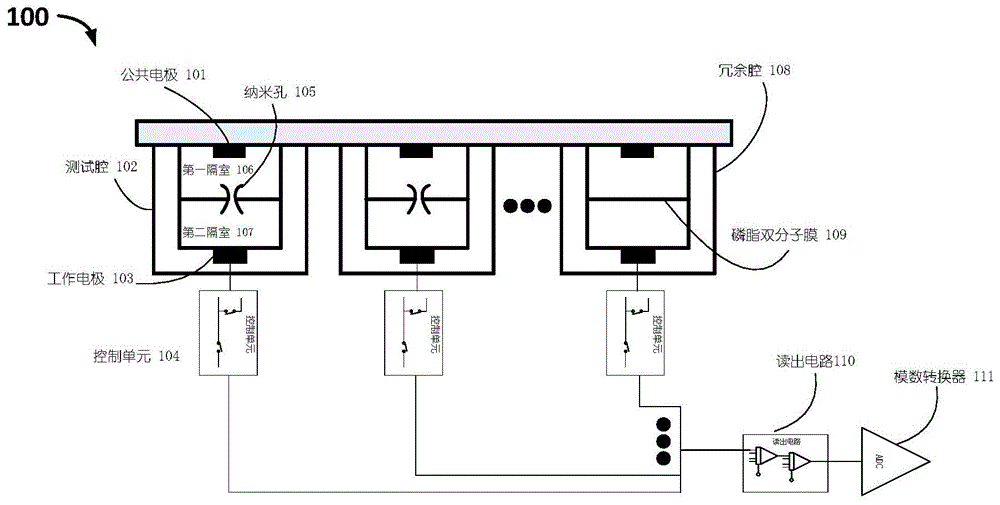
图1是根据本公开实施例的基因测序阵列结构中单个列单元的结构示意图。如图1所示,本公开实施例的基因测序阵列结构中单个列单元包括:Fig. 1 is a schematic structural diagram of a single column unit in a gene sequencing array structure according to an embodiment of the present disclosure. As shown in Figure 1, a single column unit in the gene sequencing array structure of the embodiment of the present disclosure includes:
至少一个检测单元,该检测单元包括测试腔102和连接至测试腔102的控制单元104;At least one detection unit, the detection unit includes a test cavity 102 and a control unit 104 connected to the test cavity 102;
一个冗余单元,该冗余单元包括冗余腔108和连接至冗余腔的控制单元104;a redundant unit comprising a redundant chamber 108 and a control unit 104 connected to the redundant chamber;
读出电路110,连接该检测单元和冗余单元的控制单元104,用于通过对该测试腔102和冗余腔108的累积电荷的相关双采样(CDS)来对该测试腔中的累积电荷进行转移和放大。The readout circuit 110 is connected to the control unit 104 of the detection unit and the redundant unit, and is used for detecting the accumulated charge in the test cavity by correlated double sampling (CDS) of the accumulated charge in the test cavity 102 and the redundant cavity 108 To shift and zoom in.
本公开实施例中,读出电路将检测单元的测试腔102和冗余单元的冗余腔108中累积的电荷进行转移放大,采用相关双采样的方式消除放大过程的失调电压来降低噪声。当该列单元组成基因测序阵列结构,该基因测序阵列结构可以用于对高速通过纳米孔的核苷酸类型进行判断,以实现更准确的核酸测序。In the embodiment of the present disclosure, the readout circuit transfers and amplifies the charges accumulated in the test chamber 102 of the detection unit and the redundant chamber 108 of the redundant unit, and uses correlated double sampling to eliminate the offset voltage of the amplification process to reduce noise. When the column units form a gene sequencing array structure, the gene sequencing array structure can be used to judge the type of nucleotides passing through the nanopore at high speed, so as to achieve more accurate nucleic acid sequencing.
其中,该测试腔102包括由膜109分隔的第一隔室106和第二隔室107,以及连接至第一隔室106的第一电极101(公共电极)和连接至第二隔室107的第二电极103(工作电极),所有测试腔的第一电极101连接相同的命令电压VCMD,该第二电极103连接控制单元104。在一个实施方式中,膜109可以是磷脂双分子膜,其上具有纳米孔105。Wherein, the test cavity 102 includes a first compartment 106 and a second compartment 107 separated by a membrane 109, and a first electrode 101 (common electrode) connected to the first compartment 106 and a first electrode 101 (common electrode) connected to the second compartment 107. The second electrode 103 (working electrode), the first electrodes 101 of all test chambers are connected to the same command voltage VCMD, and the second electrode 103 is connected to the control unit 104 . In one embodiment, membrane 109 may be a phospholipid bilayer membrane with nanopores 105 thereon.
类似地,该冗余腔108也包括由膜109分隔的第一隔室106和第二隔室107,以及连接至第一隔室106的第一电极101(公共电极)和连接至第二隔室107的第二电极103(工作电极),该第一电极101连接相同的命令电压VCMD,该第二电极103连接控制单元104。与测试腔102不同的是,该冗余腔108中膜109没有纳米孔105。Similarly, the redundant cavity 108 also includes a first compartment 106 and a second compartment 107 separated by a membrane 109, and a first electrode 101 (common electrode) connected to the first compartment 106 and connected to the second compartment. The second electrode 103 (working electrode) of the chamber 107 , the first electrode 101 is connected to the same command voltage VCMD, and the second electrode 103 is connected to the control unit 104 . Different from the test chamber 102 , the membrane 109 in the redundant chamber 108 has no nanopore 105 .
与测试腔102相连的该控制单元104用于周期性将测试腔102中的纳米孔膜电容重置到列参考电压,并和第一电极101形成正或者负的电压差,推动核苷酸分子通过该膜109上的纳米孔105在该第一隔室106和第二隔室107之间双向运动。由于核苷酸分子通过纳米孔105时会形成不同的纳米孔电阻(例如250MΩ~20GΩ),并导致膜电容充电或者放电电流变化,从而在采样周期(例如100μs)内形成不同的特征电压。The control unit 104 connected to the test chamber 102 is used to periodically reset the capacitance of the nanopore membrane in the test chamber 102 to the column reference voltage, and form a positive or negative voltage difference with the first electrode 101 to push the nucleotide molecule Bi-directional movement between the first compartment 106 and the second compartment 107 through the nanopore 105 on the membrane 109 . When nucleotide molecules pass through the nanopore 105, different nanopore resistances (for example, 250MΩ-20GΩ) will be formed, which will lead to changes in the charging or discharging current of the membrane capacitance, thereby forming different characteristic voltages in the sampling period (for example, 100μs).
类似地,与冗余腔108相连的该控制单元104用于周期性将冗余腔108中的膜电容重置到列参考电压。Similarly, the control unit 104 connected to the redundant chamber 108 is used to periodically reset the film capacitance in the redundant chamber 108 to the column reference voltage.
在可选的实施方式中,如图1所示,不同检测单元和冗余单元中的控制单元104还可以采取时分复用的方式依次连通读出电路110,将对应测试腔102和冗余腔108中膜109上累积的电荷转移至读出电路110中进行滤波和放大,最终输出至模数转换器111进行采样。In an optional embodiment, as shown in FIG. 1 , the control unit 104 in different detection units and redundant units can also be sequentially connected to the readout circuit 110 in a time-division multiplexing manner, and the corresponding test chamber 102 and redundant chamber The charges accumulated on the membrane 109 in 108 are transferred to the readout circuit 110 for filtering and amplification, and finally output to the analog-to-digital converter 111 for sampling.
图2是本公开实施例的基因测序的阵列结构中测试腔和冗余腔的等效电路模型示意图。如图2所示,从电学特性上,带纳米孔的测试腔201可以等效为纳米孔等效模型217,其中公共电极202和公共电极207对应,工作电极203和工作电极210对应,磷脂双分子膜205和纳米孔204则等效为等效膜电容206(例如1~2pF)和并联的纳米孔等效电阻209(例如250MΩ~20GΩ),第一隔室205中溶液等效为第一隔室等效电阻208(例如1KΩ~10KΩ),第二隔室206中溶液等效为第二隔室等效电阻211(例如1KΩ~10KΩ)。Fig. 2 is a schematic diagram of an equivalent circuit model of a test cavity and a redundant cavity in the array structure of gene sequencing according to an embodiment of the present disclosure. As shown in Figure 2, from the electrical characteristics, the test chamber 201 with nanopores can be equivalent to the nanopore equivalent model 217, wherein the common electrode 202 corresponds to the common electrode 207, the working electrode 203 corresponds to the working electrode 210, and the phospholipid double Molecular film 205 and nanopore 204 are then equivalent to equivalent film capacitance 206 (such as 1~2pF) and parallel nanopore equivalent resistance 209 (such as 250MΩ~20GΩ), and the solution in the first compartment 205 is equivalent to the first The compartment equivalent resistance 208 (eg, 1KΩ˜10KΩ), the solution in the second compartment 206 is equivalent to the second compartment equivalent resistance 211 (eg, 1KΩ˜10KΩ).
不带纳米孔的冗余腔(如图1中108),则由于没有纳米孔存在,等效为冗余单元等效模型218。其中公共电极202和公共电极213对应,工作电极203和工作电极215对应,磷脂双分子膜205等效为等效膜电容212(例如1~2pF),第一隔室205中溶液等效为第一隔室等效电阻214(例如1KΩ~10KΩ),第二隔室206中溶液等效为第二隔室等效电阻216(例如1KΩ~10KΩ)。A redundant cavity without nanoholes (108 in FIG. 1 ) is equivalent to a redundant unit equivalent model 218 because there are no nanopores. Wherein the common electrode 202 corresponds to the common electrode 213, the working electrode 203 corresponds to the working electrode 215, the phospholipid bimolecular membrane 205 is equivalent to the equivalent membrane capacitance 212 (such as 1~2pF), and the solution in the first compartment 205 is equivalent to the second The equivalent resistance 214 of the first compartment (eg, 1KΩ˜10KΩ), the solution in the second compartment 206 is equivalent to the equivalent resistance 216 of the second compartment (eg, 1KΩ˜10KΩ).
在可选的实施方式中,如图3所示,检测单元301包括复位开关303,其第一端连接列参考电压302,第二端连接测试腔等效模型217的工作电极210。还包括读出开关304,其第一端连接测试腔等效模型217的工作电极210,第二端连接读出电路110。其中,复位开关303用于周期性复位等效膜电容206,读出开关304用于周期性将等效膜电容206中累积的电荷转移到读出电路110。在可选的实施方式中,复位开关303的控制端(图3中未示出)可以连接复位信号,该复位开关303在该复位信号的作用下周期性复位等效膜电容206。复位开关303的复位周期和读出开关304的读出周期决定于系统采样率和可接受的系统信噪比。在可选的实施方式中,复位周期和读出周期至少为100μs。In an optional embodiment, as shown in FIG. 3 , the
在可选的实施方式中,如图3所示,冗余单元308包括复位开关305,其第一端连接列参考电压306,第二端连接冗余腔等效模型218的工作电极215。还包括读出开关307,其第一端连接冗余腔等效模型218的工作电极215,第二端连接读出电路110。其中,复位开关305用于周期性复位等效膜电容212,读出开关307用于周期性将等效电容212中累积的电荷转移到读出电路110。在可选的实施方式中,复位开关305的控制端(图3中未示出)可以连接复位信号,该复位开关305在该复位信号的作用下周期性复位等效膜电容212。复位开关305的复位周期和读出开关307的读出周期决定于系统采样率和可接受的系统信噪比。在可选的实施方式中,复位周期和读出周期至少为100μs。In an optional embodiment, as shown in FIG. 3 , the
图4是根据本公开一实施例的基因测序阵列结构的示意图。如图4所示,本实施例的基因测序阵列结构中,检测单元406(对应图3中的检测单元301),冗余单元407(对应图3中的冗余单元308)可以通过共享的行复位信号401、共享的列参考电压信号403以及共享的列输出信号404构成阵列。FIG. 4 is a schematic diagram of a gene sequencing array structure according to an embodiment of the present disclosure. As shown in Figure 4, in the gene sequencing array structure of this embodiment, the detection unit 406 (corresponding to the
其中,共享的行复位信号401连接至同行的每个检测单元406的第一复位开关303的控制端,用于控制其开闭从而达到重置相应检测单元的膜电容的目的,或者连接至同行的每个冗余单元407的复位开关305的控制端,用于控制其开闭从而达到重置相应冗余单元的膜电容的目的。共享的列参考电压403连接至每列的每个检测单元406的复位开关303的第一端和冗余单元407的复位开关305的第一端,用于在复位开关303或者复位开关305闭合的时候将列参考电压传递至相应的检测单元或冗余单元的工作电极。不同行的行复位信号401以时分复用的方式顺序作用。时分复用的时间宽度决定于每列中包含的检测单元和冗余单元的数量和采样周期。每列共享的列参考电压403在阵列工作过程中保持不变。每列共享的列输出信号404则在每行单元复位的同时,根据流水线阵列扫描的方向,闭合相邻行(上一行或者下一行)的检测单元的读出开关304或者冗余单元的读出开关307,输出相应单元的膜电容的累积电荷至读出电路406,从而以流水线的工作方式保证每个单元从重置到电荷输出的充放电时间最大化。Among them, the shared row
在可选的实施方案中,如图4所示,由于对应单元的工作状态可能异常,需要在工作过程中禁止该单元。因此,可以在列参考电压输入端进一步增加列复位禁止开关402,列复位禁止开关402的第一端连接列参考电压403,第二端连接每列中的检测单元406的复位开关303的第一端和冗余单元407的复位开关305的第一端,用于在选通某行单元复位的时候,从阵列外部断开其参考电压。相应地,还可以在列输出信号404连接读出电路406的中间加入列输出禁止开关405,列输出禁止开关405的第一端连接共享的列输出信号404,第二端连接读出电路406,用于在选通某行单元输出的时候,断开该单元和读出电路之间的连接。列复位禁止开关402和列输出禁止开关405能够保证需要禁止的检测单元在复位、读出和充放电过程中工作电极210始终处于浮空状态,从而保证该单元纳米孔没有电流通过而被禁止。In an optional embodiment, as shown in FIG. 4 , since the working state of the corresponding unit may be abnormal, the unit needs to be disabled during the working process. Therefore, a column
在可选的实施方式中,如图5所示,读出电路包括第一放大电路,相关双采样(Correlated Double Sampling,简称CDS)电路和第二放大电路。In an optional implementation manner, as shown in FIG. 5 , the readout circuit includes a first amplifying circuit, a correlated double sampling (Correlated Double Sampling, CDS for short) circuit and a second amplifying circuit.
相关双采样(CDS)是通常用于CCD成像中的噪音抑制技术,由于CCD每个像元的输出信号中既包含有光敏信号,也包含有复位脉冲信号,若在光电信号的积分开始时刻和积分结束时刻,分别对输出信号采样,两次采样的噪声电压相差无几,将两次采样值相减,就可以基本消除复位噪声的干扰,得到信号电平的实际有效幅值。本公开实施例基于CDS采样原理在读出电路中引入了CDS电路,用于对检测单元的测试腔和冗余单元的冗余腔中的膜电容电荷进行转移和放大存储并相减,消除第一放大电路产生的失调电压和低频噪声,从而降低电路整体噪音。Correlated Double Sampling (CDS) is a noise suppression technology commonly used in CCD imaging. Since the output signal of each pixel of CCD includes both the photosensitive signal and the reset pulse signal, if the integration of the photoelectric signal starts and At the end of the integration, the output signal is sampled separately. The noise voltage of the two samplings is almost the same. Subtracting the two sampling values can basically eliminate the interference of the reset noise and obtain the actual effective amplitude of the signal level. The embodiment of the present disclosure introduces a CDS circuit into the readout circuit based on the CDS sampling principle, which is used to transfer, amplify, store and subtract the film capacitance charges in the test chamber of the detection unit and the redundant chamber of the redundant unit, and eliminate the second Amplifies the offset voltage and low-frequency noise generated by the circuit, thereby reducing the overall noise of the circuit.
其中,第一放大电路包括运放513、反馈电容512(Cf1)和复位开关511(RST1),其中,运放513的正相输入端连接列参考电压VCM514,反相输入端连接列输出禁止开关523的第二端,列输出禁止开关523的第一端连接阵列中检测单元的读出开关507(对应图3中304)的第二端和冗余单元的读出开关510(对应图3中307)的第二端,反馈电容512和复位开关511并联在运放513的反相输入端和输出端;运放513在反馈电容512的作用下对阵列中检测单元406中存储的电荷进行转移放大,复位开关511用于对反馈电容512进行周期性复位。反馈电容512的典型值为100μF,考虑纳米孔电阻不变的情况下,对于固定的纳米孔电极压差,纳米孔充放电幅度和膜电容值成反比,而第一放大电路的增益和膜电容值成正比,因此第一放大电路最终得到的放大信号仅和纳米孔电阻相关并一一对应而和膜电容值无关。Wherein, the first amplifying circuit includes an operational amplifier 513, a feedback capacitor 512 (Cf1) and a reset switch 511 (RST1), wherein the non-inverting input terminal of the operational amplifier 513 is connected to the column reference voltage VCM514, and the inverting input terminal is connected to the column output inhibit switch The second end of 523, the first end of the column output prohibition switch 523 is connected to the second end of the readout switch 507 (corresponding to 304 in FIG. 3 ) of the detection unit in the array and the readout switch 510 of the redundant unit (corresponding to 307), the feedback capacitor 512 and the reset switch 511 are connected in parallel to the inverting input and output of the operational amplifier 513; the operational amplifier 513 transfers the charge stored in the
CDS电路包括采样电容516、采样开关515、保持开关519,CDS电容517和CDS采样开关518。其中,采样开关515的第一端连接运放513的输出端,第二端连接采样电容516和CDS电容517的第一端,用于采样或者CDS采样时将第一放大电路的电压导入采样电容516或者CDS电容517。保持开关519的第一端连接至CDS电容517的第二端,用于将CDS采样后存储在采样电容516和CDS电容517中的电荷转移到第二放大电路。采样电容516的第一端连接采样开关515的第二端,第二端连接列参考电压VCM514。CDS电容517的第一端连接采样开关515的第二端,第二端连接保持开关519的第一端。CDS采样开关518的第一端连接CDS电容517的第二端,第二端连接列参考电压VCM514,用于存储CDS采样时第一放大电路的输出。The CDS circuit includes a sampling capacitor 516 , a sampling switch 515 , a hold switch 519 , a CDS capacitor 517 and a CDS sampling switch 518 . Wherein, the first end of the sampling switch 515 is connected to the output end of the operational amplifier 513, and the second end is connected to the first end of the sampling capacitor 516 and the CDS capacitor 517, and is used for sampling or CDS sampling when the voltage of the first amplifying circuit is introduced into the sampling capacitor 516 or CDS capacitor 517. The first end of the holding switch 519 is connected to the second end of the CDS capacitor 517 for transferring the charge stored in the sampling capacitor 516 and the CDS capacitor 517 after CDS sampling to the second amplifying circuit. The first end of the sampling capacitor 516 is connected to the second end of the sampling switch 515 , and the second end is connected to the column reference voltage VCM514 . The first terminal of the CDS capacitor 517 is connected to the second terminal of the sampling switch 515 , and the second terminal is connected to the first terminal of the holding switch 519 . The first end of the CDS sampling switch 518 is connected to the second end of the CDS capacitor 517 , and the second end is connected to the column reference voltage VCM514 for storing the output of the first amplifying circuit during CDS sampling.
第二放大电路包括运放522、反馈电容521(Cf2)和复位开关520(RST2)。其中,运放522的正相输入端连接至列参考电压VCM514,反相输入端连接至保持开关519的第二端。反馈电容521和复位开关520并联在运放522的反相输入端和输出端。运放522在反馈电容521的作用下对CDS电路的输出进行电荷转移和进一步放大。复位开关520用于对反馈电容521进行周期性复位。第二放大电路的增益由CDS电容517和采样电容516的串联电容值和反馈电容521的电容值的比值决定,反馈电容521的电容典型值为100μF,而第二放大电路的增益典型值为2~3,因此CDS电容517和采样电容516的串联电容典型值为200~300μF。The second amplifying circuit includes an operational amplifier 522, a feedback capacitor 521 (Cf2) and a reset switch 520 (RST2). Wherein, the non-inverting input end of the operational amplifier 522 is connected to the column reference voltage VCM514 , and the inverting input end is connected to the second end of the holding switch 519 . The feedback capacitor 521 and the reset switch 520 are connected in parallel to the inverting input terminal and the output terminal of the operational amplifier 522 . The operational amplifier 522 performs charge transfer and further amplification on the output of the CDS circuit under the action of the feedback capacitor 521 . The reset switch 520 is used to periodically reset the feedback capacitor 521 . The gain of the second amplifying circuit is determined by the ratio of the capacitance value of the series connection of the CDS capacitor 517 and the sampling capacitor 516 to the capacitance value of the feedback capacitor 521, the typical value of the capacitance of the feedback capacitor 521 is 100 μF, and the typical value of the gain of the second amplifying circuit is 2 ~3, so the typical value of the series capacitance of the CDS capacitor 517 and the sampling capacitor 516 is 200-300 μF.
图6是根据图5所示的读出电路的信号波形示意图,表示图5所示的读出电路运行时具体的时序。如图6所示,对于阵列中任意检测单元,其工作时序分为自动归零602、采样603和保持604,总长度单元采样周期T 601为系统采样周期/列检测单元数量。如无特别说明,列输出禁止开关523在后续描述中始终闭合。波形图中RST是图5中列复位开关506的控制信号,RST_DUMMY是图5中冗余单元复位开关508的控制信号,SMP是图5中列读出开关507的控制信号,SMP_DUMMY是图5中冗余单元读出开关510的控制信号,RST1是图5中第一放大电路复位开关511的控制信号,RST2是图5中第二放大电路复位开关520的控制信号,CDS2是图5中CDS采样开关518的控制信号,以上开关控制信号在高电平时使对应开关闭合,低电平时使对应开关断开。CDS1是图5中采样开关515和保持开关519的控制信号,高电平时使保持开关519闭合,采样开关515断开,低电平时使保持开关519断开,采样开关515闭合。FIG. 6 is a schematic diagram of signal waveforms according to the readout circuit shown in FIG. 5 , showing specific timing when the readout circuit shown in FIG. 5 is running. As shown in Figure 6, for any detection unit in the array, its working sequence is divided into automatic zeroing 602, sampling 603 and hold 604, and the total length unit sampling period T 601 is the system sampling period/number of detection units in a column. Unless otherwise specified, the column output disable switch 523 is always closed in the following descriptions. In the waveform diagram, RST is the control signal of the column reset switch 506 in FIG. 5, RST_DUMMY is the control signal of the redundant unit
其中,当电路处于自动归零602状态时,采样开关515和CDS采样开关518一直闭合,保持开关519断开,列读出开关507断开。复位开关511首先快速将反馈电容512重置后断开,然后开启冗余单元读出开关510,冗余腔505中膜电容的存储电压值以及第一放大电路可能的失调电压叠加转移至CDS电容517并放大,然后断开冗余单元读出开关510和CDS采样开关518。由于冗余腔采样之前存储的电压为参考电压VCM,因此此时CDS电容517中存储的是经过放大的第一放大电路的失调值。Wherein, when the circuit is in the auto-zero 602 state, the sampling switch 515 and the CDS sampling switch 518 are always closed, the holding switch 519 is open, and the
当电路处于采样状态603时,复位开关511首先快速将反馈电容512重置后断开,然后开启检测单元列读出开关507,由于采样开关515闭合,此时测试腔502中膜电容在采样周期中累积的电压将转移至采样电容516并放大。在进入保持状态604之前,第二放大电路和冗余单元电路将被重置。另外,在读出检测单元电荷的同时,其前一行的检测单元由于电荷在上个采样周期被读出,本周期将被重启并开始下一轮充放电过程。本状态结束时采样电容516中存储的是测试腔的膜电容的累积电压叠加运放513失调电压后的放大结果。When the circuit is in the sampling state 603, the reset switch 511 first quickly resets the feedback capacitor 512 and then disconnects it, and then opens the detection unit
当电路处于保持状态604时,检测单元列读出开关507断开,采样开关515断开,保持开关519闭合,此时存储于采样电容516的电压将减去存储于CDS电容517中的电压,并转移至反馈电容521中进一步放大,形成最终的电压送往模数转换单元采样。由于冗余单元和检测单元的膜是在相同的生化条件下生成,因此可以期望其具有相近的电容值,因此,第一放大电路对于检测单元和冗余单元的增益倍数应近似相等。通过CDS电路的转换可以认为运放513的失调电压将在运放522的输出中基本被消掉。When the circuit is in the holding state 604, the detection unit
本公开还提出一种基因测序装置,该基因测序装置包括如前述任一实施例所述的阵列结构。The present disclosure also proposes a gene sequencing device, which includes the array structure as described in any one of the foregoing embodiments.
本公开实施例的基因测序阵列结构及其装置采用电荷转移的方式直接测量测试腔和冗余腔的累积电荷,并采用相关双采样的方式消除读出电路放大过程中的失调电压,降低检测噪声,从而可以对高速通过纳米孔的核苷酸类型进行判断,以实现更准确的核酸测序。The gene sequencing array structure and its device in the embodiments of the present disclosure directly measure the accumulated charges of the test cavity and the redundant cavity by means of charge transfer, and use correlated double sampling to eliminate the offset voltage during the amplification process of the readout circuit and reduce the detection noise , so that the type of nucleotide passing through the nanopore at high speed can be judged to achieve more accurate nucleic acid sequencing.
应当说明的是,上述实施例均可根据需要自由组合。以上所述仅是本公开的优选实施方式,应当指出,对于本技术领域的普通技术人员来说,在不脱离本公开原理的前提下,还可以做出若干变化和改进,这些变化和改进也应视为落入本公开的保护范围。It should be noted that the above embodiments can be freely combined as required. The above descriptions are only preferred implementations of the present disclosure. It should be pointed out that those skilled in the art can make several changes and improvements without departing from the principles of the present disclosure. These changes and improvements are also should be considered as falling within the protection scope of the present disclosure.
Claims (10)
Priority Applications (2)
| Application Number | Priority Date | Filing Date | Title |
|---|---|---|---|
| CN202010256084.0A CN113493735B (en) | 2020-04-02 | 2020-04-02 | Gene sequencing array structure and gene sequencing device |
| PCT/CN2021/085322 WO2021197481A1 (en) | 2020-04-02 | 2021-04-02 | Gene sequencing array structure and gene sequencing apparatus |
Applications Claiming Priority (1)
| Application Number | Priority Date | Filing Date | Title |
|---|---|---|---|
| CN202010256084.0A CN113493735B (en) | 2020-04-02 | 2020-04-02 | Gene sequencing array structure and gene sequencing device |
Publications (2)
| Publication Number | Publication Date |
|---|---|
| CN113493735A CN113493735A (en) | 2021-10-12 |
| CN113493735B true CN113493735B (en) | 2023-06-16 |
Family
ID=77927414
Family Applications (1)
| Application Number | Title | Priority Date | Filing Date |
|---|---|---|---|
| CN202010256084.0A Active CN113493735B (en) | 2020-04-02 | 2020-04-02 | Gene sequencing array structure and gene sequencing device |
Country Status (2)
| Country | Link |
|---|---|
| CN (1) | CN113493735B (en) |
| WO (1) | WO2021197481A1 (en) |
Citations (7)
| Publication number | Priority date | Publication date | Assignee | Title |
|---|---|---|---|---|
| CN1681290A (en) * | 2004-03-16 | 2005-10-12 | 三星电子株式会社 | Method and circuit for performing correlated double sub-sampling (CDSS) of pixels in an active pixel sensor (APS) array |
| WO2010117470A2 (en) * | 2009-04-10 | 2010-10-14 | Pacific Biosciences Of California, Inc. | Nanopore sequencing devices and methods |
| CN102301228A (en) * | 2008-10-22 | 2011-12-28 | 生命技术公司 | Integrated Sensor Arrays for Biological and Chemical Analysis |
| CN103297031A (en) * | 2013-04-23 | 2013-09-11 | 北京航空航天大学 | Circuit and method for reading correlated double sampling brain electric signal collection |
| CN104076138A (en) * | 2011-07-20 | 2014-10-01 | 加利福尼亚大学董事会 | Compensated patch-clamp amplifier for nanopore polynucleotide sequencing and other applications |
| WO2018050730A1 (en) * | 2016-09-15 | 2018-03-22 | F. Hoffmann-La Roche Ag | Nanopore-based sequencing using voltage mode with hybrid mode stimuli |
| CN110741097A (en) * | 2017-04-19 | 2020-01-31 | 豪夫迈·罗氏有限公司 | Phased Nanopore Arrays |
Family Cites Families (3)
| Publication number | Priority date | Publication date | Assignee | Title |
|---|---|---|---|---|
| CA2823787C (en) * | 2011-07-20 | 2017-04-11 | The Regents Of The University Of California | A dual-pore dual-amplifier device providing independently adjustable voltages across each pore |
| CA2861457A1 (en) * | 2012-01-20 | 2013-07-25 | Genia Technologies, Inc. | Nanopore based molecular detection and sequencing |
| GB2500715A (en) * | 2012-03-30 | 2013-10-02 | Gene Onyx Ltd | Single nucleotide polymorphism detection using an ISFET array |
-
2020
- 2020-04-02 CN CN202010256084.0A patent/CN113493735B/en active Active
-
2021
- 2021-04-02 WO PCT/CN2021/085322 patent/WO2021197481A1/en not_active Ceased
Patent Citations (7)
| Publication number | Priority date | Publication date | Assignee | Title |
|---|---|---|---|---|
| CN1681290A (en) * | 2004-03-16 | 2005-10-12 | 三星电子株式会社 | Method and circuit for performing correlated double sub-sampling (CDSS) of pixels in an active pixel sensor (APS) array |
| CN102301228A (en) * | 2008-10-22 | 2011-12-28 | 生命技术公司 | Integrated Sensor Arrays for Biological and Chemical Analysis |
| WO2010117470A2 (en) * | 2009-04-10 | 2010-10-14 | Pacific Biosciences Of California, Inc. | Nanopore sequencing devices and methods |
| CN104076138A (en) * | 2011-07-20 | 2014-10-01 | 加利福尼亚大学董事会 | Compensated patch-clamp amplifier for nanopore polynucleotide sequencing and other applications |
| CN103297031A (en) * | 2013-04-23 | 2013-09-11 | 北京航空航天大学 | Circuit and method for reading correlated double sampling brain electric signal collection |
| WO2018050730A1 (en) * | 2016-09-15 | 2018-03-22 | F. Hoffmann-La Roche Ag | Nanopore-based sequencing using voltage mode with hybrid mode stimuli |
| CN110741097A (en) * | 2017-04-19 | 2020-01-31 | 豪夫迈·罗氏有限公司 | Phased Nanopore Arrays |
Also Published As
| Publication number | Publication date |
|---|---|
| CN113493735A (en) | 2021-10-12 |
| WO2021197481A1 (en) | 2021-10-07 |
Similar Documents
| Publication | Publication Date | Title |
|---|---|---|
| CN112994680B (en) | Multi-channel switching circuit and switching method | |
| US10663423B2 (en) | System for detecting electrical properties of a molecular complex | |
| CN104303050B (en) | For controlling, detecting and measuring the sensor circuit of molecular complex | |
| US20240426772A1 (en) | Current measurement apparatus, molecular entity sensing apparatus, method of measuring a current, method of sensing a molecular entity | |
| CN107850627A (en) | For measuring the apparatus and method of electric current | |
| CN112708544A (en) | Measuring device and measuring method for gene sequencing | |
| US10203297B2 (en) | Device and method for detecting redox reactions in solution | |
| CN113493735B (en) | Gene sequencing array structure and gene sequencing device | |
| US9222908B2 (en) | Device and method for detecting redox reactions in solution | |
| US10822654B2 (en) | Sequencing biopolymers | |
| Dong et al. | A 37.37 μW-per-cell multifunctional automated nanopore sequencing CMOS platform with 16∗ 8 biosensor array | |
| WO2023038830A1 (en) | A circuit design to apply different voltages in a nanopore array | |
| CN113740397B (en) | Microcurrent detection circuit and gene sequencing device | |
| CN115047243B (en) | A current detection circuit for DNA sequencing | |
| CN115901907A (en) | Nanopore sequencing circuit unit and gene sequencing device | |
| US20240409993A1 (en) | Analog circuit to compensate bias offset in amplifier array | |
| US20230070552A1 (en) | Circuit design to apply different voltages in a nanopore array | |
| WO2023039414A1 (en) | A circuit design to measure small current variation in nanopore sequencing | |
| GB2586339A (en) | Current measurement apparatus, molecular entity sensing apparatus, method of measuring a current, method of sensing a molecular entity | |
| CN121186433A (en) | A measurement circuit for detecting weak currents in a multichannel nanopore system |
Legal Events
| Date | Code | Title | Description |
|---|---|---|---|
| PB01 | Publication | ||
| PB01 | Publication | ||
| SE01 | Entry into force of request for substantive examination | ||
| SE01 | Entry into force of request for substantive examination | ||
| GR01 | Patent grant | ||
| GR01 | Patent grant |