CN113412531A - Device and method for operating a charged particle device with a plurality of beamlets - Google Patents
Device and method for operating a charged particle device with a plurality of beamlets Download PDFInfo
- Publication number
- CN113412531A CN113412531A CN202080013100.1A CN202080013100A CN113412531A CN 113412531 A CN113412531 A CN 113412531A CN 202080013100 A CN202080013100 A CN 202080013100A CN 113412531 A CN113412531 A CN 113412531A
- Authority
- CN
- China
- Prior art keywords
- beamlet
- deflector
- beamlets
- scanner
- charged particle
- Prior art date
- Legal status (The legal status is an assumption and is not a legal conclusion. Google has not performed a legal analysis and makes no representation as to the accuracy of the status listed.)
- Granted
Links
Images


Classifications
-
- H—ELECTRICITY
- H01—ELECTRIC ELEMENTS
- H01J—ELECTRIC DISCHARGE TUBES OR DISCHARGE LAMPS
- H01J37/00—Discharge tubes with provision for introducing objects or material to be exposed to the discharge, e.g. for the purpose of examination or processing thereof
- H01J37/02—Details
- H01J37/04—Arrangements of electrodes and associated parts for generating or controlling the discharge, e.g. electron-optical arrangement or ion-optical arrangement
- H01J37/147—Arrangements for directing or deflecting the discharge along a desired path
- H01J37/1472—Deflecting along given lines
- H01J37/1474—Scanning means
-
- G—PHYSICS
- G01—MEASURING; TESTING
- G01N—INVESTIGATING OR ANALYSING MATERIALS BY DETERMINING THEIR CHEMICAL OR PHYSICAL PROPERTIES
- G01N21/00—Investigating or analysing materials by the use of optical means, i.e. using sub-millimetre waves, infrared, visible or ultraviolet light
- G01N21/84—Systems specially adapted for particular applications
- G01N21/88—Investigating the presence of flaws or contamination
- G01N21/95—Investigating the presence of flaws or contamination characterised by the material or shape of the object to be examined
- G01N21/9501—Semiconductor wafers
-
- G—PHYSICS
- G01—MEASURING; TESTING
- G01N—INVESTIGATING OR ANALYSING MATERIALS BY DETERMINING THEIR CHEMICAL OR PHYSICAL PROPERTIES
- G01N23/00—Investigating or analysing materials by the use of wave or particle radiation, e.g. X-rays or neutrons, not covered by groups G01N3/00 – G01N17/00, G01N21/00 or G01N22/00
- G01N23/22—Investigating or analysing materials by the use of wave or particle radiation, e.g. X-rays or neutrons, not covered by groups G01N3/00 – G01N17/00, G01N21/00 or G01N22/00 by measuring secondary emission from the material
- G01N23/225—Investigating or analysing materials by the use of wave or particle radiation, e.g. X-rays or neutrons, not covered by groups G01N3/00 – G01N17/00, G01N21/00 or G01N22/00 by measuring secondary emission from the material using electron or ion
- G01N23/2251—Investigating or analysing materials by the use of wave or particle radiation, e.g. X-rays or neutrons, not covered by groups G01N3/00 – G01N17/00, G01N21/00 or G01N22/00 by measuring secondary emission from the material using electron or ion using incident electron beams, e.g. scanning electron microscopy [SEM]
-
- H—ELECTRICITY
- H01—ELECTRIC ELEMENTS
- H01J—ELECTRIC DISCHARGE TUBES OR DISCHARGE LAMPS
- H01J37/00—Discharge tubes with provision for introducing objects or material to be exposed to the discharge, e.g. for the purpose of examination or processing thereof
- H01J37/02—Details
- H01J37/04—Arrangements of electrodes and associated parts for generating or controlling the discharge, e.g. electron-optical arrangement or ion-optical arrangement
- H01J37/10—Lenses
-
- H—ELECTRICITY
- H01—ELECTRIC ELEMENTS
- H01J—ELECTRIC DISCHARGE TUBES OR DISCHARGE LAMPS
- H01J37/00—Discharge tubes with provision for introducing objects or material to be exposed to the discharge, e.g. for the purpose of examination or processing thereof
- H01J37/26—Electron or ion microscopes; Electron or ion diffraction tubes
- H01J37/261—Details
- H01J37/265—Controlling the tube; circuit arrangements adapted to a particular application not otherwise provided, e.g. bright-field-dark-field illumination
-
- H—ELECTRICITY
- H01—ELECTRIC ELEMENTS
- H01J—ELECTRIC DISCHARGE TUBES OR DISCHARGE LAMPS
- H01J37/00—Discharge tubes with provision for introducing objects or material to be exposed to the discharge, e.g. for the purpose of examination or processing thereof
- H01J37/26—Electron or ion microscopes; Electron or ion diffraction tubes
- H01J37/28—Electron or ion microscopes; Electron or ion diffraction tubes with scanning beams
-
- G—PHYSICS
- G01—MEASURING; TESTING
- G01N—INVESTIGATING OR ANALYSING MATERIALS BY DETERMINING THEIR CHEMICAL OR PHYSICAL PROPERTIES
- G01N2223/00—Investigating materials by wave or particle radiation
- G01N2223/30—Accessories, mechanical or electrical features
- G01N2223/33—Accessories, mechanical or electrical features scanning, i.e. relative motion for measurement of successive object-parts
- G01N2223/3301—Accessories, mechanical or electrical features scanning, i.e. relative motion for measurement of successive object-parts beam is modified for scan, e.g. moving collimator
-
- G—PHYSICS
- G01—MEASURING; TESTING
- G01N—INVESTIGATING OR ANALYSING MATERIALS BY DETERMINING THEIR CHEMICAL OR PHYSICAL PROPERTIES
- G01N2223/00—Investigating materials by wave or particle radiation
- G01N2223/30—Accessories, mechanical or electrical features
- G01N2223/33—Accessories, mechanical or electrical features scanning, i.e. relative motion for measurement of successive object-parts
- G01N2223/3308—Accessories, mechanical or electrical features scanning, i.e. relative motion for measurement of successive object-parts object translates
-
- G—PHYSICS
- G01—MEASURING; TESTING
- G01N—INVESTIGATING OR ANALYSING MATERIALS BY DETERMINING THEIR CHEMICAL OR PHYSICAL PROPERTIES
- G01N2223/00—Investigating materials by wave or particle radiation
- G01N2223/60—Specific applications or type of materials
- G01N2223/611—Specific applications or type of materials patterned objects; electronic devices
- G01N2223/6116—Specific applications or type of materials patterned objects; electronic devices semiconductor wafer
-
- H—ELECTRICITY
- H01—ELECTRIC ELEMENTS
- H01J—ELECTRIC DISCHARGE TUBES OR DISCHARGE LAMPS
- H01J2237/00—Discharge tubes exposing object to beam, e.g. for analysis treatment, etching, imaging
- H01J2237/04—Means for controlling the discharge
- H01J2237/045—Diaphragms
- H01J2237/0451—Diaphragms with fixed aperture
- H01J2237/0453—Diaphragms with fixed aperture multiple apertures
-
- H—ELECTRICITY
- H01—ELECTRIC ELEMENTS
- H01J—ELECTRIC DISCHARGE TUBES OR DISCHARGE LAMPS
- H01J2237/00—Discharge tubes exposing object to beam, e.g. for analysis treatment, etching, imaging
- H01J2237/10—Lenses
- H01J2237/103—Lenses characterised by lens type
-
- H—ELECTRICITY
- H01—ELECTRIC ELEMENTS
- H01J—ELECTRIC DISCHARGE TUBES OR DISCHARGE LAMPS
- H01J2237/00—Discharge tubes exposing object to beam, e.g. for analysis treatment, etching, imaging
- H01J2237/15—Means for deflecting or directing discharge
- H01J2237/151—Electrostatic means
- H01J2237/1516—Multipoles
-
- H—ELECTRICITY
- H01—ELECTRIC ELEMENTS
- H01J—ELECTRIC DISCHARGE TUBES OR DISCHARGE LAMPS
- H01J2237/00—Discharge tubes exposing object to beam, e.g. for analysis treatment, etching, imaging
- H01J2237/153—Correcting image defects, e.g. stigmators
- H01J2237/1534—Aberrations
-
- H—ELECTRICITY
- H01—ELECTRIC ELEMENTS
- H01J—ELECTRIC DISCHARGE TUBES OR DISCHARGE LAMPS
- H01J2237/00—Discharge tubes exposing object to beam, e.g. for analysis treatment, etching, imaging
- H01J2237/26—Electron or ion microscopes
- H01J2237/28—Scanning microscopes
- H01J2237/2801—Details
-
- H—ELECTRICITY
- H01—ELECTRIC ELEMENTS
- H01J—ELECTRIC DISCHARGE TUBES OR DISCHARGE LAMPS
- H01J2237/00—Discharge tubes exposing object to beam, e.g. for analysis treatment, etching, imaging
- H01J2237/26—Electron or ion microscopes
- H01J2237/28—Scanning microscopes
- H01J2237/2809—Scanning microscopes characterised by the imaging problems involved
- H01J2237/2811—Large objects
Landscapes
- Chemical & Material Sciences (AREA)
- Analytical Chemistry (AREA)
- Physics & Mathematics (AREA)
- Health & Medical Sciences (AREA)
- Life Sciences & Earth Sciences (AREA)
- Biochemistry (AREA)
- General Health & Medical Sciences (AREA)
- General Physics & Mathematics (AREA)
- Immunology (AREA)
- Pathology (AREA)
- Electron Sources, Ion Sources (AREA)
- Electron Beam Exposure (AREA)
Abstract
A method of operating a charged particle beam device is disclosed, the method comprising passing each beamlet of a plurality of beamlets through a deflector (6) and a scanner (12) in sequence. Each of the beamlets is focused with an objective lens onto the sample to form a plurality of focal spots, thereby forming an array. The first beamlet (4A) is focused on the first spot (40A) and the second beamlet (4D) is focused on the second spot (40D). In a centered configuration of the device, each beamlet of the plurality of beamlets is directed by the deflector towards a coma-free point (100). In a beamlet-shifted configuration of the apparatus, the scanner is scanned such that the first beamlet passes through an acceptable aberration point (105), the first beamlet scanning the shifted first field of view; and the first spot is shifted from the regular first focal spot to the shifted first focal spot (45A).
Description
Technical Field
Embodiments described herein relate to charged particle beam devices for use in inspection, defect detection, and/or critical dimension applications. Embodiments also relate to methods of operating a charged particle beam device, such as a device comprising a beamlet of more than one charged particle. Multi-beam systems can be used for general purposes such as imaging, and for high-throughput Electron Beam Inspection (EBI). Embodiments may also relate to a scanning charged particle beam device and an inspection method using a scanning charged particle beam device such as a Scanning Electron Microscope (SEM).
Background
Charged particle beam devices have many uses, such as inspecting semiconductor devices having nanoscale features. Modern semiconductor technology is highly dependent on precise control of the various processes used during integrated circuit production. Therefore, the semiconductor wafer is inspected to detect problems. In addition, the mask or reticle (reticle) may be inspected to ensure that the mask or reticle accurately defines the desired pattern.
Inspection of a wafer or mask for defects may include inspection of the entire wafer or mask area. Therefore, it is challenging to inspect large areas with high resolution. Furthermore, as soon as possible, it is desirable to perform the inspection quickly so that production yield is not limited by the inspection process, if possible.
Scanning Electron Microscopy (SEM) has been used to inspect wafers. The wafer surface may be scanned using a well focused electron beam. When the electron beam irradiates the wafer, secondary electrons and/or backscattered electrons, i.e., signal electrons, are generated and detected. For example, a defect at a certain location on the wafer may be detected by comparing the intensity signal of the secondary electrons with a reference signal corresponding to the same location on the pattern.
Wafer and mask defect inspection in semiconductor technology benefits from high resolution and fast inspection tools that can cover complete wafer/mask applications and/or hot spot inspection. The electron beam can be used to provide high resolution inspection of the sample, enabling small defects to be detected. In particular, from the 20nm node and above, the high resolution potential of electron beam based imaging tools is required to detect many defects of interest.
However, scanning the entire surface of the wafer can take a long time due to the reduction in feature size and the increased demand for higher resolution. Therefore, using a single beam Scanning Electron Microscope (SEM) for wafer inspection may not be ideal due to yield limitations. Thus, a multi-beam SEM is required. For example, multiple beams or beamlets may allow inspection to be performed at multiple locations on the sample simultaneously, thereby increasing throughput. However, when using a multi-beam system requiring innovative solutions, a number of technical difficulties may be encountered, such as the difficulty of generating, controlling and manipulating a plurality of charged particle beams.
Disclosure of Invention
A method of operating a charged particle beam device (1) is disclosed, the method comprising passing each beamlet of a plurality of beamlets (4A, 4D) through a deflector (6) and a scanner (12). The beamlets pass through the scanner after passing through the deflector. Each of the beamlets is focused with an objective lens onto the sample to form a plurality of focal spots (focal spots) to form an array. The first beamlet is focused on a first spot (spot) and the second beamlet is focused on a second spot. In a centered configuration of the device, each beamlet of the plurality of beamlets is directed by the deflector towards a coma-free point on a virtual plane perpendicular to the optical axis; the first spot (40A) is a regular (regular) first focal spot (40A) formed by the first beamlet (4A); and the scanner is scanned. In the arrangement of beamlet displacement of the device (fig. 4), the scanner is scanned, optionally synchronized with the deflector, such that the first beamlet (4A) passes through the acceptable aberration point 105 on the virtual plane (210), the first beamlet 4A scanning the displaced first field of view 405A; and the first spot (40A or 45A) is shifted from the regular first focal spot (40A) to the shifted first focal spot (45A).
Disclosed herein is a charged particle beam apparatus comprising a source of charged particles and a multi-well plate comprising a plurality of wells, each well for passing a beamlet therethrough, the multi-well plate forming a plurality of beamlets of charged particles. The device still includes: a deflector; a scanner; and an objective lens configured to focus the plurality of beamlets on the plurality of focal spots to form an array comprising a first beamlet focused on a first spot and a second beamlet focused on a second spot. The charged particle beam device has a centered configuration and a beamlet shifted configuration. In the centered configuration, the deflector is configured to direct each beamlet of the plurality of beamlets towards a coma-free point on a virtual plane perpendicular to the optical axis, and the plurality of focal spots includes a first spot that is a regular first focal spot formed by the first beamlet. In the beamlet shifted configuration, the scanner and the deflector are each configured to be scanned such that the deflector deflects the first beamlet through an acceptable aberration point on the virtual plane and the first beamlet scans the shifted first field of view and the first spot is shifted from the regular first focal spot to the shifted first focal spot.
Embodiments are also directed to apparatuses for performing the disclosed methods and including apparatus components for performing each of the described method features. The method features may be performed by hardware components, such as a computer and/or a controller. The computer and/or controller may be configurable, programmable, configured and/or programmed, such as by appropriate software. Further, embodiments are also directed to methods that may be performed by the described apparatus. Embodiments include method features for performing each function of a device.
Drawings
So that the manner in which the above recited features can be understood in detail, a more particular description, briefly summarized above, may be had by reference to embodiments. The figures relate to embodiments and are described below:
FIG. 1 shows a schematic view of a charged particle beam device according to embodiments described herein;
fig. 2 shows a portion of a charged particle device in a centered configuration according to embodiments described herein;
fig. 3A shows a portion of a charged particle device in a centered configuration according to embodiments described herein;
fig. 3B shows a portion of a charged particle device in a centered configuration according to embodiments described herein;
fig. 4 shows a portion of a charged particle device in a beamlet shifted configuration according to embodiments described herein;
fig. 5 shows a portion of a charged particle device in a beamlet shifted configuration according to embodiments described herein;
fig. 6 shows a portion of a charged particle device in a beamlet shifted configuration according to embodiments described herein;
fig. 7 illustrates a method of operating a charged scanning device according to embodiments described herein.
Detailed Description
Reference will now be made in detail to the various embodiments, one or more examples of which are illustrated in the figures. In the following description of the drawings, like reference numerals refer to like parts. Differences with respect to the various embodiments are described. Each example is provided by way of explanation and is not meant as a limitation. Furthermore, features illustrated or described as part of one embodiment can be used on or in conjunction with other embodiments to yield yet a further embodiment. The present embodiments are intended to include modifications and variations.
Without limiting the scope of protection of the present application, in the following, a charged particle beam device or a component thereof may be referred to as a charged particle beam device or "device", which may comprise components for detecting secondary or backscattered particles (such as electrons). Embodiments may include devices and components that may detect secondary and/or backscattered charged particles in the form of electrons, ions, photons, X-rays, and/or other signals that may be used to obtain an image of a sample. As described herein, the discussion and description of detection is exemplary with respect to electrons in a scanning electron microscope. Other types of charged particles (e.g., positive ions) can be detected by the device in a variety of different instruments.
Herein, a primary charged particle beam or primary charged particle beamlet may be generated by a particle beam source and may be directed to a sample to be examined and/or imaged.
Herein, the beam may be a primary beam; the beamlets may be primary beamlets. The primary beam or beamlets are used to illuminate the sample. The primary beamlets may be beamlets for illuminating the sample.
According to embodiments herein, which may be combined with other embodiments, the signal beam of charged particles may refer to a beam of secondary particles and/or backscattered particles. Typically, the signal beam or the secondary beam is generated by the impact of the primary beam or primary beamlets on the sample and/or by the backscattering of the primary beam from the sample.
Reference herein to "specimen" or "sample" includes, but is not limited to, semiconductor wafers, semiconductor workpieces, photolithographic masks, and other workpieces, such as memory disks and the like. Embodiments may be applied to any workpiece on which a material is deposited or structured. The sample may comprise a surface to be structured or a surface on which a layer is deposited, an edge, and typically a bevel.
Fig. 1 shows a charged particle beam device 1 comprising a plurality of charged particle beamlets 4A, 4D, 4G according to an embodiment. The device may be used for sample examination. The charged particle beam device 1 comprises a charged particle source 2, which charged particle source 2 can generate charged particles, which are guided to a perforated plate 5. The wells 5A, 5D, 5G of the multi-well plate 5 can pass through the thin bundles 4A, 4D, 4G, respectively. Each of the beamlets may pass through the scanner 12 after passing through the deflector 6.
The beamlets may be focused by the objective lens 10 to form a plurality of focal spots 40A, 40D. The first beamlet 4A is focused on the first spot 40A and the second beamlet 4D is focused on the second spot 40D.
The charged particle beam device 1 comprises a deflector 6, which deflector 6 may comprise deflector elements 6A, 6D, which deflector elements 6A, 6D may direct the beamlets 4A, 4D, respectively, towards the objective lens 10. The deflector elements 6A, 6D are addressable by a controller 110. The deflector elements 6A, 6D may be configured such that each deflector element passes one of the beamlets. The deflector elements 6A, 6D may comprise a first deflector element 6A and a second deflector element 6D. The first deflector element 6A may pass the first beamlets 4A. The second deflector element 6D may pass the second beamlet 4D. MEM may be operated to energize each deflector element simultaneously. The deflector 6 may comprise MEM. The MEM may be configured to generate an electric multipole (multipole) such as a dipole (dipole), a quadrupole (quadrupole), a hexapole (hexapole), an octapole (octupole), and/or higher multipoles at each deflector element 6A, 6D.
The controller 110 may address each deflector element 6A, 6D. The controller 110 may send a first signal to the first deflector element 6A and a second signal to the second deflector element 6D. The first signal and the second signal may be the same or may be different. The second signal may be the same as the additional signal sent by the controller 110 to the additional deflector element of the deflector 6. The controller 110 may control each deflector element 6A, 6D, for example, such that each deflector element 6A, 6D receives a unique signal, or receives the same signal.
The deflector 6 may make the beamlets appear to come from spatially separated sources. Alternatively/additionally, the charged particle beam device 1 may comprise a collecting mirror (not shown), which may be placed, for example, between the source 2 and the perforated plate 5. The condenser lens may direct the charged particles directly to the perforated plate 5. Alternatively/additionally, the condenser lens may be placed after the perforated plate 5, such as immediately after the perforated plate 5. The condenser lens may directly or indirectly collimate the charged particles and/or direct them towards the objective lens 10.
The deflector 6 and the scanner 12 may be configured for synchronization, and the lenslet 300 or lenslet array may also be synchronized with the deflector and/or scanner. The controller 110 can synchronize the scanning of the scanner 12 with the scanning of the deflector 6 and the optional lenslet 300 or lenslet array. The controller 110 may control the configuration of the charged particle device 1, such as switching between a centered configuration and a beamlet shifted configuration.
The deflector 6 and/or the scanner 12 may move the charged particle beamlets 4A, 4D, 4G over the sample 8. The sample 8 may be on a platform 7 (such as a translatable platform), the platform 7 may also assist in moving the sample 8, thereby facilitating imaging and/or examination of the sample 8.
When the beamlets 4A, 4D, 4G strike the surface of the sample 8, they may undergo interaction with the sample. The interaction may produce various emissions, such as electrons, X-rays, heat, and light. Many of these emissions may be used to generate images of the sample and/or collect data from the sample 8. The emission of interest for examination or image formation comes from signal electrons escaping from the sample 8 at various angles at relatively low energies (1eV to 50 eV). Signal electrons including backscattered electrons and/or secondary electrons may be collected from the sample by the objective lens 10. The secondary electrons may be separated from the backscattered electrons and/or beamlets 4A, 4D, 4G in a beam splitter assembly, which may be placed in the optical path such that the signal electrons collected by the objective lens 10 may be directed to a detector assembly. The detector assembly may comprise a detector element which may be configured to generate a measurement signal, e.g. an electrical signal which corresponds electronically to the detected signal. The computer and/or controller may receive data generated by the device.
By illuminating the sample with the beamlets 4A, 4D, 4G and displaying and/or recording the output of the detector assembly, data for inspection/testing of the sample may be provided, including a plurality of images of the surface of the sample 8. Each image may provide information about a different portion of the sample surface. Thus, the speed of data acquisition can be increased by using multiple beamlets as compared to a single beam device. The platform 7 (or sample support) may be movable, such as may be moved horizontally in all directions. This may allow the beamlets 4A, 4D, 4G to reach a target area to be examined on the sample.
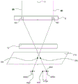
Fig. 1 also shows a coma-free point 100, the coma-free point 100 being shown in the objective lens 10. The coma-free point 100 may alternatively be located in the scanner 12 or between the scanner and the objective lens 10. The beamlets 4A, 4D, 4G can be seen to pass through the coma free point 100. By passing through the coma-free point 100, aberrations can be reduced and/or minimized, and the focused beamlet spot size can be reduced and/or minimized to improve resolution. The scanner 12 may operate to dynamically shift the beamlets 4A, 4D such that they intermittently and/or periodically pass through the coma-free point 100 during scanning.
The scanner 12 may add aberrations such as astigmatism, coma, and field curvature (field) aberrations. The scan range over which the size of the field of view may be determined and/or selected may be based on the amount of acceptable aberration and/or loss of resolution. Larger range and/or field of view may lead to larger aberrations, larger beamlet focal spot sizes, and deteriorated resolution.
In one example, the array of focal spots of the beamlets extends to a radius of about 80 μm, e.g., the array of beamlets is placed on a virtual ring of a radius of about 80 μm; the field of view of one of the beamlets may be about ± 5 μm. If the scan range is larger than this, a significant loss of spatial resolution may result, such as an increase in spot size of 5% or more. The scanner 12 may add significant aberrations. Alternatively/additionally, the operation of the scanner may be limited to maintain resolution, or at least maintain acceptable resolution. For example, if the beamlets 4A, 4D are scanned intermittently and/or periodically relatively far from the coma-free point 100, the spot size of the beamlets increases at a location far from the coma-free point 100 and the resolution, particularly near the outer edge of the field of view, may get worse. At relatively high scan ranges, beamlet aberrations may reach unacceptably high levels, such that the spot size becomes unacceptably large and the resolution unacceptably poor. What is acceptable and what is unacceptable may be predetermined or selected.
In one embodiment, the range of scanning by the scanner 12 can be limited such that the aberrations are not more than acceptable, such as limiting the aberrations such that the spot size increases by less than 1%, 2%, 5%, or 10% from the spot size when the beam passes through the coma-free point 100. If we define a virtual plane 210 (see fig. 2) perpendicular to the optical axis 0, the acceptable aberration point 105 can be defined as the point on the virtual plane 210 that includes the coma-free point 100. The acceptable aberration point 105 may be a point on the virtual plane 210 through which the beamlets may pass, which may result in the spot size of the focused beamlets increasing less than a predetermined amount over the spot size of the beamlets passing through the coma-free point 100; the predetermined amount may be 10%, 5%, 2%, or 1%.
The scanner 12 can dynamically shift the beamlets 4A, 4D from the coma-free point 100, which can increase astigmatism, coma, and field curvature. It may be technically challenging to find an operating method and associated hardware (such as optics and controllers) arrangement that can minimize aberrations while providing a charged particle device that can operate with a large field of view with excellent spatial resolution capability, especially when fast throughput is desired as in semiconductor inspection applications.
Fig. 2 illustrates a centered configuration of an apparatus according to embodiments described herein. In the centered configuration of the device, the deflector 6 directs each of the plurality of beamlets 4A, 4D towards a coma-free point 100 on the virtual plane 210.
The coma-free point may be located in the field of the objective lens 10, such as in the objective lens 10 (e.g. as seen in fig. 1), i.e. e.g. not in the field-free region. The coma-free point 100 may be located on the optical axis 0. The coma-free point 100 may be located in the scanner 12, such as the center of the scanner 12. The coma-free point 100 may be located between the objective lens 10 and the scanner 12. The coma-free point may be located in the field of at least one of the scanner 12, the objective lens 10 and the electrostatic lens for decelerating the charged particle beam before the charged particle beam hits the sample, or at a position between the scanner 12, the objective lens 10 and the electrostatic lens for decelerating.
Fig. 2 shows beamlets 4A, 4D focused by the objective lens 10 to form a plurality of focal spots 40A, 40D. The first beamlet 4A is focused on the first spot 40A and the second beamlet 4D is focused on the second spot 40D. The plurality of focal spots may form an array, such as a regularly spaced array. As shown in fig. 2, the focal spot may be located on a virtual ring 25, and the virtual ring 25 may be centered on the optical axis 0. The focal spots 40A, 40D may be located on a focal plane 20, such as the focal plane 20 perpendicular to the optical axis 0.
When the device is in the centered configuration, the first spot 40A is referred to as a regular first focal spot 40A.
In embodiments that may be combined with other embodiments described herein, the beamlets may be scanned such as by operation of the scanner 12 and the deflector 6, in particular by scanning the scanner 12 and the deflector 6 synchronously, such that the beamlets pass through the coma-free point 100.
Fig. 3A illustrates a centered configuration of an apparatus according to embodiments described herein. Fig. 3A shows a virtual plane 210 comprising the coma-free point 100 and the focal spots 40A, 40D of the beamlets 4A, 4D. For simplicity of illustration, the objective lens 10 is not shown in fig. 3A. The objective lens 10 is understood to be placed behind the scanner 12. In the centered configuration, the regular first focal spot 40A may be centered in the first field of view, which may be considered as a regular first field of view 400A. The second beamlets 4D may form second focal spots 40D, which second focal spots 40D may be centered in the second field of view 400D. The deflector 6 may direct each of the beamlets 4A, 4D towards the coma-free point 100. The scanner 12 may scan the beamlets 4A, 4D such that respective fields of view 400A, 400D of the first 4A and second 4D beamlets are illuminated by the beamlets 4A, 4D during the scanning, while the charged particle device is in a centered configuration.
Fig. 3B illustrates a centered configuration of an apparatus according to embodiments described herein. In the centered configuration, at least a first beamlet 4A (such as each beamlet 4A, 4D) directed by the deflector 6 towards the coma-free point 100 may be dynamically deflected away from the coma-free point 100, such as by the scanner 12 during scanning. Each of the beamlets 4A, 4D, including those directed by the deflector 6 towards the coma-free point 100, may be deflected by the scanner 12 during scanning. Manipulation of the beamlets by the scanner 12 may cause the beamlets to pass through the virtual plane 210 at a point displaced from the coma-free point 100. Each beamlet 4A, 4D may intermittently and/or periodically pass through the coma-free point 100, such as passing through the coma-free point 100 synchronously with the scanning frequency.
The scanner 12 may be arranged such that each beam is approximately equally dynamically offset, thereby causing approximately the same dynamic offset for each beam. The regular first focal spot 40A and the second focal spot 40D may be positioned such that the first beamlet 4A and the second beamlet 4D each pass through the coma free point 100 during scanning. The regular first focal spot 40A and the second focal spot 40D may be within respective fields of view, such as within a first field of view 400A and a second field of view 400D, respectively, as shown in fig. 3A and 3B. The regular first focal spot 40A and the second focal spot 40D may be centered within their respective fields of view, the first field of view 400A and the second field of view 400D.
If the deflector 6 statically deflects (and/or directs) the first beamlet 4A towards the acceptable aberration point 105 and the scanner 12 dynamically deflects the beamlets 4A, 4D, the first beamlet 4A may pass through the virtual plane 210 at a point oscillating around the acceptable aberration point 105. If the oscillation is too large, undesirable spot size increases and resolution loss may result.
In fig. 3B, the first beamlet 3A is shown as being deflected by the scanner, forming beam paths 33A and 33A'. The beam paths 33A, 33A' may pass through the virtual plane 210 at points displaced from the coma-free point 100 to the edges of the regular field of view 400A. The range of scanning and/or the fields of view 400A, 400D may be limited to a predetermined range. The predetermined range may be based on an increase in acceptable spot size, which may be associated with a tolerable loss of resolution at the edges of the field of view.
The increase in spot size and loss of resolution tend to scale with the degree of displacement of the beamlets from the coma-free point on virtual plane 210. It may be useful to determine the limits of the scan parameters, such as the field of view 400A, by reference to the acceptable aberration points 105 (see fig. 4). For example, in the centered configuration, the regular first field of view 400A of the first beamlets 4A may be limited such that when the first beamlets 4A reach the edge of the regular first field of view 400A, the first beamlets 4A pass through the centrally configured acceptable aberration point 104, 104'.
The scanner 12 may deflect the beamlets 4A, 4D such that at a maximum deflection of the scanner 12, the beamlets 4A, 4D reach an acceptable aberration point. The extent of the field of view 400A, 400D of the beamlets 4A, 4D may be determined by the acceptable aberration points and/or the associated loss of resolution of the beamlets passing through the virtual plane at maximum deflection.
The scanner 12 may be multi-polar, such as hexapole, octopole, or higher. The charged beam device is configured such that for each beam, separate astigmatism and multi-polar (such as hexapole or higher) correction can be applied, such as by adjusting the deflector element 6A, 6D corresponding to each beamlet 4A, 4D.
Directing the beamlets to a region of interest outside the regular field of view of the beamlets may be technically difficult without significant loss of resolution. In some configurations of charged particle devices, hot spots or other areas of interest may be relatively poorly resolved (resolved).
Fig. 4 shows a configuration of beamlet displacement of the charged particle beam device 1 according to embodiments described herein. As in fig. 3A and 3B, the objective lens 10 is not shown in fig. 4 for the sake of simplifying the description. The objective lens 10 is understood to be below the scanner 12. As shown in fig. 4, in the beamlet-shifted configuration, the deflector 6 may deflect the first beamlet 4A towards the acceptable aberration point 105, while the deflector 6 deflects the second beamlet 4D towards the coma-free point 100.
In the beamlet shifted configuration, the acceptable aberration point 105 may be shifted from the coma-free point 100. The focal spot of the first beamlet 4A may be shifted from the regular first focal spot 40A (see fig. 3) to the shifted first focal spot 45A. There may be a maximum beamlet shift of the first focal spot related to an acceptable aberration point 105 and/or a predetermined acceptable increase (e.g. 1%, 2%, 5%, or 10%) of the spot size, such as for a centered configuration.
In the beamlet-shifted configuration, the first beamlet 4A may be used to illuminate and/or image a region of interest, such as a hot spot, while the second beamlet 4D or any number of other beamlets of the plurality may operate similarly/identically as in the centered configuration. In other words, it is possible to direct one of the beamlets, for example the first beamlet 4A, to a region of interest such as a hot spot, while the other beamlets 4D, 4G of the array may continue to operate as in a centered configuration. It may be advantageous if each of the deflector elements 6A, 6D for each of the beamlets 4A, 4D is individually addressable. The deflector 6 may be configured so as to deflect each of the beamlets 4A, 4D separately, such as deflecting each of the beamlets 4A, 4D independently of the other beamlets.
In the beamlet-shifted configuration, the scanner 12 and the deflector 6 may be scanned such that the first beamlet 4A passes through the acceptable aberration point 105 on the virtual plane 210. The scanning may be such that the first beamlets 4A continuously pass the acceptable aberration point 100 during the scanning. Alternatively, the scanning may be performed such that the first beamlet 4A oscillates around the acceptable aberration point 100 in synchronization with the scanning, such as if the deflector 6 statically directs the first beamlet 4A towards the acceptable aberration point 105; first beamlets 4A may intermittently or periodically pass through an acceptable aberration point.
The displaced first focal spot 45A may be directed at a hot spot and/or location of the sample 8 of particular interest. It is desirable to be able to adjust at least one beamlet of the array, such as any beamlet of the array, to be able to illuminate a point of interest or "hot spot". Hotspots, etc. may be located at such locations: in a typical configuration of a charged particle device, each of the beamlets 4A, 4D cannot reach said position without significant loss of resolution due to significant aberrations. It may be desirable to operate the charged particle device such that resolution loss is minimized even when illuminating/imaging hot spots that may be located anywhere on the sample.
As shown in fig. 4, the displaced first spot 45A may be centered in the displaced field of view 405A of the first beamlet 4A. The second spot 40D may be centered in a second field of view 400D formed by the second beamlet 4D. The second light spot 40D and/or the second field of view 400D may not be distinguishable in the centered configuration and the beam shifted configuration of the charged particle beam device 1. The deflector 6 may direct the first beamlet 4A towards the acceptable aberration point 105.
In a shifted beamlet configuration, the first beamlet 4A may illuminate the shifted first field of view 405A. The shifted first spot 45A may be shifted from the regular first focal spot 40A by a first beamlet offset 415A. In a configuration of displacing beamlets, the deflector 6 may move the first beamlet 4A towards hot spots or the like that are not on a regular array (e.g. or ring) formed by the plurality of beamlets 4A, 4D. In other words, in a beamlet-shifted configuration, the first spot of the first beamlet 4A may be shifted from the array of focal spots formed by the beamlets, or, in case a plurality of focal spots in a centered configuration form a ring, from the ring.
Disclosed herein are methods and apparatus that utilize multiple deflections of a beamlet (e.g., a first beamlet), particularly in a shifted beamlet configuration, to optimize the beamlet path to meet possible goals, such as reducing noise, maintaining acceptable resolution, minimizing aberrations, and/or increasing scan rate, particularly when using beamlets to illuminate/image hot spots.
Fig. 5 shows a configuration of a displaced beamlet of a charged particle device, according to embodiments disclosed herein. The shifted field of view 405A may be illuminated by the first beamlet 4A, which first beamlet 4A may continuously pass the acceptable aberration point 105 on the virtual plane 210. The deflector 6 may direct the first beamlet 4A towards an acceptable aberration point 105, taking into account the deflection due to the scanner 12. Fig. 5 shows two optical paths 44A, 44A 'of the first beamlet 4A, the optical paths 44A, 44A' each reaching an edge of the field of the shifted field of view 405A of the first beamlet. The deflector element 6A may deflect the first beamlet 4A along the optical path 44A, 44A' to reach the edge of the displaced field of view 405A. The displaced first focal spot 45A may be located in the displaced field of view 405A, such as in the center of the displaced field of view 405A. The scanning of the deflector 6, or more specifically the first deflector element 6A, may compensate the deflection of the scanner 12 such that the first beamlets 4A continuously pass the acceptable aberration point 105. In other words, the deflector 6 may be scanned synchronously with the scanner 12, such that the first beamlet 4A continuously passes the acceptable aberration point 105, while the other beamlets 4D, 4G are statically directed towards the coma-free point 100.
In yet another embodiment, the deflector 6 is scanned synchronously with the scanner 12, such that the first beamlet continuously passes the acceptable aberration point 105, while the other beamlets 4D, 4G are statically directed towards the coma-free point 100. In embodiments that may be combined with any other embodiments disclosed herein: each of the plurality of beamlets 4A, 4D is scanned by a scanner 12; the first beamlets 4A are scanned by a deflector 6; and the second beamlet 4D is statically deflected by the deflector 6 towards the coma-free point 100.
Fig. 5 also shows lenslets 300 that can correct for the field curvature aberration of the first beamlets 4A. For each beamlet 4A, 4D of the plurality of beamlets 4A, 4D, there may be an array of lenslets to correct the field curvature of the respective beamlet. Each lenslet of the lenslet array may be addressed by the controller 110 and may be scanned in synchronization with the scanner 12 and/or deflector 6. The corrected field curvature of the first beamlet 4A or any of the beamlets may be synchronized with the scanning of the scanner 12 and/or the deflector 6. Each of the lenslets (such as lenslet 300 for the first beamlet 4A) may be scanned in synchronization with the scanner and/or deflector.
As shown in fig. 5, pre-deflection of the beamlet(s) by deflector 6 may keep the beamlet(s) at an acceptable aberration point 105 when illuminating a region of interest, such as a hot spot outside the regular field of view of any of the beamlets in a centered configuration. The dynamic astigmatism correction and the hexapole correction may further extend the respective fields of view of the beamlets in the plurality of beamlets. As an example, the field of view obtainable when the beamlets are pre-deflected by the deflector has a range of about 5-10 μm.
The controller may comprise electronics configured to address each of the deflector elements 6A, 6D of the deflector 6. The controller may provide fast switching voltages to sub-elements, such as poles, of the deflector elements 6A, 6D of the deflector 6. The controller may provide signals and/or powers suitable for deflecting the beamlets 4A, 4D by at least one of the deflector elements 6A, 6D in synchronization with the scanner 12. The relative phase and amplitude of the synchronous control signals and/or power signals to the deflector 6 and scanner 12 (and optionally the lenslet array) may be adjustable.
Each deflector element 6A, 6D may be configured to pass one of the beamlets 4A, 4D. The deflector may comprise a MEM configured to generate an electric or higher dipole at each deflector element 6A, 6D of the deflector 6. MEM may be configured to simultaneously generate a dipole, a quadrupole and a hexapole at each deflector element 6A, 6D. For example, each deflector element 6A, 6D comprises 8 or more poles/electrodes, in particular for simultaneously generating dipoles, quadrupoles and hexapoles. Higher order MEMs are also envisaged, such as MEMs comprising e.g. up to 20 poles/electrodes or even higher deflector elements 6A, 6D.
Each deflector element 6A, 6D may be configured to generate a field statically and/or dynamically (including a superposition of static and dynamic fields), such as may be determined by a signal and/or power from a controller. Each deflector element 6A, 6D may be configured to operate in unison with or independently of the other deflector elements, such as by a controller.
For an array of beamlets arranged in a virtual ring of radius 80 μm, the possible offset of the beamlets from a regular focal spot towards a region of interest (or hot spot) may be extended up to about 20 μm by dynamic correction of the curvature of field of the lenslets 300 (and/or lenslet array), and by dynamic pre-deflection of the deflector 6, and the field of view of each beamlet is allowed to be about 20 μm. At an acceptable loss of resolution, it is advantageous to have a possible large deviation from the regular array and a possible large field of view.
Fig. 6 illustrates a configuration of shifting beamlets according to embodiments described herein. For clarity, the objective lens 10 is not shown, the objective lens 10 being understood to be below the scanner 12 (further along the optical axis). Fig. 6 also does not show the other beamlets 6D, 6G of the plurality. Other beamlets should also be understood to be present, which pass through the optical element similar to that previously described. For example, the second beamlet 4D (and/or any other beamlets of the plurality of beamlets) may be directed towards a coma-free point by the deflector 6 and the scanner 12.
The deflector 6 may include a first MEM 61 and a second MEM 62. The first MEM 61 and the second MEM 62 may be arranged along the optical axis 0. Each beamlet 4A, 4D may pass through the first MEM 61 and the second MEM 62 sequentially. The controller may control each of the first MEM 61 and the second MEM 62 by controlling the deflector 6. The controller 110 may address the individual elements 61A, 61D, 62A, 62D of each MEM. The first beamlets 4A may be sequentially deflected by the first deflector element 61A of the first MEM 61 and subsequently by the first deflector element 62A of the second MEM 62. The second beamlets 4D may be sequentially deflected by the second deflector elements 62A of the first MEM 61 and subsequently by the second deflector elements 62D of the second MEM 62.
The deflector may comprise a first MEM and a second MEM such that in the beamlet shifted configuration, the acceptable aberration point is the minimum aberration point 111 on a virtual plane 210 comprising the coma-free point 100, and the first beamlet 4A passes continuously through the minimum aberration point 111. The controller and MEM may be configured such that any one of the beamlets 4A, 4D of the plurality of beamlets may be deflected by the deflector 6 and the scanner 12 such that the beamlets successively pass the point of minimum aberration 111.
The first and second MEM 61, 62 may be used to aim the first beamlet 4A (or any beamlet) at a region or hot spot of interest to keep the beamlet at the point of minimum aberration 111. The hexapole correction and astigmatism correction can be optimized. By dynamic correction of the field curvature of the lenslets in synchronization with dynamic pre-deflection by the MEM deflector, in synchronization with the scanner 12, it is possible to reduce aberrations and/or keep beamlets passing through the point of minimum aberration.
In one embodiment, the minimum aberration point 111 is a point on a virtual plane 210 that includes the coma-free point 100 through which the scanning beamlet may pass continuously, the minimum aberration point 111 being such that the beamlet maintains a reasonable minimum spot size when focused on a continuous portion of the focal plane. A reasonable minimum spot size may be larger than 10%, 5%, 2%, or 1% larger than the spot size when the beamlets pass through a coma-free point to the center of the centrally arranged field of view. The continuous portion of the focal plane may be different from the normal field of view.
The minimum aberration point 111 may correspond to the centrally arranged coma free point 100.
For an array of beamlets arranged in a virtual ring with a radius of 80 μm, the possible offset of the beamlets from a regular focal spot towards a region of interest (or hot spot) can be extended up to about 40 μm by dynamic correction of the curvature of field of the lenslets 300 (and/or lenslet array) and by dynamic pre-deflection of the deflector 6 using two MEMs in series, and allowing a field of view of each beamlet to be about 40 μm.
In an embodiment, in the beamlet-shifted configuration, the scanner 12 and the deflector 6 are scanned synchronously such that the first beamlet 4A continuously passes the point of minimum aberration 111, such as to the shifted first focal spot 45A shifted from the centrally configured regular first focal spot 40A. It is possible that when scanning the shifted first field of view 405A by the first beamlets 4A of the minimum aberration point 111, the second beamlets 4D pass the coma free point 100 and scan the regular second field of view 400D.
The deflector 6, scanner 12, and lenslet 300 or lenslet array may be synchronized, such as by the controller 110. The lenslet array may be configured to correct the field curvature aberration of the first beamlets 4A independently of the second beamlets 4D, especially when the charged particle beam device 1 is in a beamlet-shifted configuration. The lenslet arrays may be positioned directly adjacent, such as directly above or directly below the deflector 6.
In general, the scanner 12 may be configured to scan all beamlets 4A, 4D simultaneously in synchronization with each other. In a beamlet-shifted configuration, the deflector 6 may dynamically deflect one or more of the beamlets (such as a first beamlet) in synchronization with the scanner, while the deflector 6 statically deflects other beamlets (e.g., including a second beamlet) towards a coma-free point. The dynamic deflection of the deflector 6 may direct a beamlet (such as the first beamlet 4A) such that the coefficients continuously pass the acceptable aberration point 105 and/or the minimum aberration point 111.
Embodiments may include first and second MEMs configured to dynamically correct astigmatism in synchronization with scanning by a scanner in a beamlet shifted configuration. The deflector may comprise at least one deflector element (and/or MEM element), such as two deflector elements (and/or MEM elements), for each beamlet passing through the deflector. Each MEM element may produce a dipole or higher pole.
One or each of the MEMs may be configured to generate an electric or higher pole at each deflector element of the deflector 6. The MEM(s) may be (individually) configured to simultaneously generate a dipole, a quadrupole, and a hexapole at each deflector element. For example, each deflector element comprises 8 or more poles/electrodes, in particular for simultaneously generating dipoles, quadrupoles and hexapoles. Higher order MEMs are also envisaged, such as MEMs comprising deflector elements having, for example, up to 20 poles/electrodes or even more.
Each deflector element of the MEM(s) may be configured to generate a field (including a superposition of static and dynamic fields) statically and/or dynamically, such as may be determined by a signal and/or power from a controller. Each deflector element may be configured to operate in unison with or independently of the other deflector elements, such as by a controller. When there are two MEMs, each beamlet may pass through a unique pair of deflector elements, one deflector element per MEM provided, and each unique pair of deflector elements may be dynamically operated in synchronization, in particular for minimizing aberrations in the configuration of beamlet displacement.
The controller 110 may be configured to control the configuration of the charged particle device 1, such as to switch between a centered configuration and a beamlet shifted configuration. The controller 110 may select which beamlets of the plurality of beamlets are to be shifted. The controller 110 can control, synchronize and/or power the scanning of the scanner 12 and the scanning of the deflector 6 (or any one or more elements thereof), and optionally the scanning of the lenslet array (or any one or more lenslets therein).
High speed electronics for MEMS and/or lenslets are further contemplated and disclosed herein. Such high speed electronic devices may include multiple channels. For example, in controlling a MEM having 8 poles/electrodes, each MEM element may have up to 8 channels controlled by the controller 110 at high speed in synchronization with the scanner 12. For simplicity, a MEMS with 4 poles may be advantageous.
Fig. 7 illustrates a method of operating a charged scanning device 500 according to embodiments described herein. The plurality of beamlets pass through a deflector and scanner 510. The device operates in a centered configuration 520 and the device operates in a beamlet shifted configuration 530. The beamlets are focused 540 on the sample with an objective lens.
The present disclosure is intended to include the following enumerated embodiments, wherein reference to the reference numbers and figures are mentioned to aid understanding, without reference or with the intent to be limiting:
1. a method of operating a charged particle beam device (1), comprising:
passing each beamlet of the plurality of beamlets (4A, 4D) through a deflector (6) and a scanner (12), wherein the beamlets pass the scanner after passing the deflector;
focusing each of the plurality of beamlets (4A, 4D) on the sample with an objective lens (10) to form a plurality of focal spots (40A, 40D) constituting an array, the focusing comprising focusing a first beamlet (4A) on a first spot (40A) and focusing a second beamlet on a second spot (40D);
in the centered configuration of the device,
directing each beamlet of the plurality of beamlets towards a coma-free point (100) on a virtual plane (210) perpendicular to the optical axis with a deflector (6), wherein
The first spot (40A) is a regular first focal spot (40A) formed by the first beamlet (4A), and
scanning the scanner 12 such that each beamlet of the beamlets scans a regular field of view, comprising a first field of view of a first beamlet scanning rule and a second field of view of a second beamlet scanning rule; and
in the beamlet-shifted configuration of the device (figure 4),
scanning the scanner such that the first beamlet (4A) passes through the acceptable aberration point 105 on the virtual plane (210), the first beamlet 4A scanning the shifted first field of view 405A, wherein
The first spot (40A or 45A) is shifted from the regular first focal spot (40A) to the shifted first focal spot (45A).
In a beamlet-shifted configuration, the scanner and deflector may be scanned (such as synchronously) such that the first beamlet passes through an acceptable aberration point.
2. The method of operating a charged particle beam device as claimed in embodiment 1, wherein,
in the configuration in which the beamlets are displaced,
the displaced first field of view (405A) is displaced from the regular first field of view (400A) in a direction substantially perpendicular to the optical axis, and
the scanner is scanned such that the second beamlets scan a regular second field of view. The scanner may synchronously scan each of the beamlets, e.g., such that each respective field of view is scanned from each beamlet simultaneously.
3. The method of operating a charged particle beam device of any preceding embodiment, wherein,
in the centered configuration, the regular first focal spot (40A) is centered in a regular first field of view (400A) of the first beamlet (4A); and is
In the beamlet shifted configuration, the shifted first spot (45A) is centered in the shifted field of view of the first beamlet.
4. The method of operating a charged particle beam device of any preceding embodiment, wherein
In the centered configuration and the beamlet shifted configuration, the second spot (40D) is centered in a regular second field of view (400D) of the second beamlet.
5. The method of operating a charged particle beam device of any preceding embodiment, wherein
In the centered configuration, the arrays are regularly spaced. In a beamlet-shifted configuration, at least one of the beamlets (such as the first beamlet) may be focused at a position deviating from the regular spot of the beamlet.
6. The method of operating a charged particle beam device of any preceding embodiment, wherein
A centered configuration such that each focal spot of the array is arranged on a virtual ring; and
in the beamlet shifted configuration, the first spot is shifted from the virtual ring.
7. The method of operating a charged particle beam device of any preceding embodiment, wherein
The deflector comprises a MEM configured to generate at least an electric dipole and an electric quadrupole at each deflector element (6A, 6D) of the deflector (6); and each deflector element is configured to pass one of the beamlets. The MEM may also be configured to produce hexapoles. The MEM may have 8 poles/electrode. The MEM may be configured to produce even higher multipoles, such as up to 20.
8. The method of operating a charged particle beam device of any preceding embodiment, wherein
Acceptable aberration points are shifted from coma-free points on the virtual plane; wherein
A coma-free point is located in the field of the objective lens.
9. The method of operating a charged particle beam device of any preceding embodiment, wherein
In the centered configuration and in the beamlet-shifted configuration, each of the beamlets is scanned by a scanner; and
in the configuration of beamlet displacement, the first beamlet is scanned by the deflector, and
the second beamlet is statically deflected by the deflector towards the coma-free point. The scanner may synchronously scan each of the beamlets. The deflector may scan the first beamlet in synchronization with the scanner.
10. The method of operating a charged particle beam device of any preceding embodiment, further comprising:
the first beamlets are passed through lenslets, which correct for field curvature of the first beamlets. The lenslets may be modulated in synchronization with the scanning of the scanner.
11. The method of operating a charged particle beam device of embodiment 10, wherein
Correcting the field curvature of the first beamlet in synchronism with the scanning by the scanner and/or deflector; and the lenslets scan synchronously with the scanner and/or deflector.
12. The method of operating a charged particle beam device of any preceding embodiment, wherein
The deflector comprises a first MEM and a second MEM, such that in a beamlet shifted configuration,
the acceptable aberration point is the minimum aberration point, and
during the scanning by the scanner and the scanning by the deflector, the first beamlets successively pass the points of minimum aberration.
13. The method of operating a charged particle beam device of any preceding embodiment, wherein
In the beamlet-shifted configuration, the scanning deflector comprises:
the first beamlets are scanned so as to deflect the first beamlets dynamically while the second beamlets are deflected statically.
14. The method of operating a charged particle beam device of any preceding embodiment, wherein,
in the beamlet-shifted configuration, the scanner and deflector are scanned synchronously so that the first beamlet continuously passes through the acceptable aberration point.
15. A charged particle beam device, comprising:
a source of charged particles and a multi-well plate comprising a plurality of wells, each well for passing a beamlet therethrough, the multi-well plate forming a plurality of beamlets of charged particles;
a deflector;
a scanner;
an objective lens configured to focus the plurality of beamlets on a plurality of focal spots to form an array comprising a first beamlet focused on a first spot and a second beamlet focused on a second spot; and
wherein
The charged particle beam device has a centered configuration and a beamlet shifted configuration; wherein
In the centered configuration, the center of gravity,
the deflector is configured to direct each beamlet of the plurality of beamlets towards a coma-free point on a virtual plane perpendicular to the optical axis, and
the plurality of focal spots comprises a first spot being a regular first focal spot formed by a first beamlet; and
in the configuration in which the beamlets are displaced,
the scanner and the deflector are each configured to be scanned such that
The deflector deflects the first beamlet through an acceptable aberration point on a virtual plane, an
The first beamlet scans the shifted first field of view, wherein
The first spot is shifted from the regular first focal spot to the shifted first focal spot.
16. The charged particle beam device of embodiment 15, further comprising
A lenslet array configured to correct field curvature aberrations of a first beamlet independently of a second beamlet when the charged particle beam device is in the beamlet shifted configuration.
17. The charged particle beam device of embodiment 15 or embodiment 16, wherein
The scanner is configured to simultaneously scan each beamlet of the plurality of beamlets in synchronization; and
in the configuration in which the beamlets are displaced,
the deflector is configured to dynamically deflect the first beamlet in synchronization with the scanner, and
the deflector is configured to statically deflect the second beamlet towards the coma-free point.
18. The charged particle beam device of embodiment 15, embodiment 16, or embodiment 17, wherein the deflector comprises a first MEM and a second MEM, the first MEM and the second MEM being configured such that,
in the beamlet shifted configuration, the acceptable aberration point is the minimum aberration point, and
the deflector and the scanner are configured for synchronization such that the first beamlet continuously passes the point of minimum aberration.
19. The charged particle beam device of embodiment 15, embodiment 16, or embodiment 17 or embodiment 18, wherein
The deflector comprises a first MEM and a second MEM, and
the first MEM and the second MEM are configured in a beamlet shifted configuration to dynamically correct astigmatism in synchronization with scanning by the scanner. Each MEM may be configured to produce a dipole, a quadrupole, a hexapole, and combinations thereof. Each MEM may also produce higher multipoles, such as up to 20.
20. The charged particle beam device of any of embodiments 15-19, comprising
A controller that controls a configuration of the charged particle beam device, wherein the scanner and the deflector are controlled by the controller; and wherein the controller synchronizes the scanner and the deflector.
21. The charged particle beam device of any one of embodiments 15-20, wherein
The deflector includes a MEM configured to generate an electric or higher pole (such as a dipole, quadrupole, and hexapole); and
the scanning deflector is a deflector that dynamically deflects at least one beamlet, such as in synchronization with scanning by the scanner.
While the foregoing is directed to embodiments of the present disclosure, other and further embodiments of the disclosure may be devised without departing from the basic scope thereof, and the scope thereof is determined by the claims that follow.
Claims (20)
1. A method of operating a charged particle beam device, comprising:
passing each beamlet of a plurality of beamlets through a deflector and a scanner, wherein the beamlets pass through the scanner after passing through the deflector;
focusing each beamlet of the plurality of beamlets on the sample with an objective lens to form a plurality of focal spots comprising an array, the focusing comprising focusing a first beamlet on a first spot and focusing a second beamlet on a second spot;
in the centered configuration of the device,
directing each beamlet of the plurality of beamlets with the deflector toward a coma-free point on a virtual plane perpendicular to an optical axis, wherein
The first spot is a regular (regular) first focal spot formed by the first beamlet, and
scanning the scanner such that each of the beamlets scans a regular field of view, including a first field of view of the first beamlet scanning rule and a second field of view of the second beamlet scanning rule; and
in the beamlet-shifted configuration of the device,
scanning the scanner such that the first beamlets pass through acceptable aberration points on the virtual plane, the first beamlets scanning a shifted first field of view, wherein
The first spot is shifted from the regular first focal spot to the shifted first focal spot.
2. The method of operating the charged particle beam device of claim 1,
in the configuration in which the beamlets are displaced,
the shifted first field of view is shifted from the regular first field of view in a direction substantially perpendicular to the optical axis, and
the scanner is scanned such that the second beamlets scan the regular second field of view.
3. The method of operating the charged particle beam device of any preceding claim,
in the centered configuration, the regular first focal spot is centered in a regular first field of view of the first beamlet; and is
In the beamlet shifted configuration, the shifted first spot is centered in the shifted field of view of the first beamlet.
4. Method of operating a charged particle beam device as claimed in any of the preceding claims, wherein
In the centered configuration and the beamlet-shifted configuration, the second spot is centered in a regular second field of view of the second beamlet.
5. Method of operating a charged particle beam device as claimed in any of the preceding claims, wherein
In the centered configuration, the arrays are regularly spaced.
6. Method of operating a charged particle beam device as claimed in any of the preceding claims, wherein
The centered configuration is such that each focal spot of the array is arranged on a virtual ring; and
in the beamlet-shifted configuration, the first light spot is shifted from the virtual ring.
7. Method of operating a charged particle beam device as claimed in any of the preceding claims, wherein
The deflector comprises a MEM configured to generate at least an electric dipole (dipole) and an electric quadrupole (quadrupole) at each deflector element of the deflector; and each deflector element is configured to pass one of the beamlets.
8. Method of operating a charged particle beam device as claimed in any of the preceding claims, wherein
The acceptable aberration point is displaced from the coma-free point on the virtual plane; wherein
The coma-free point is located in the field of the objective lens.
9. Method of operating a charged particle beam device as claimed in any of the preceding claims, wherein
In the centered configuration and in the beamlet-shifted configuration, each of the beamlets is scanned by the scanner; and
in the configuration of the beamlet displacement, the first beamlet is scanned by the deflector, and
the second beamlet is statically deflected by the deflector towards the coma-free point.
10. The method of operating the charged particle beam device of any preceding claim, further comprising:
the first beamlets are passed through lenslets, which correct for field curvature (field curvature) of the first beamlets.
11. The method of operating the charged particle beam device of claim 10, wherein
Correcting the field curvature of the first beamlet in synchronism with the scanning of the scanner and/or the deflector; and the lenslets scan synchronously with the scanner and/or deflector.
12. Method of operating a charged particle beam device as claimed in any of the preceding claims, wherein
The deflector comprises a first MEM and a second MEM, such that in the beamlet shifted configuration,
the acceptable aberration point is a minimum aberration point, and
the first beamlets pass the point of minimum aberration continuously during the scanning by the scanner and the scanning by the deflector.
13. Method of operating a charged particle beam device as claimed in any of the preceding claims, wherein
In the beamlet-shifted configuration, scanning the deflector comprises:
scanning the first beamlets so as to dynamically deflect the first beamlets while statically deflecting the second beamlets.
14. The method of operating the charged particle beam device of any preceding claim,
in the beamlet-shifted configuration, the scanner and deflector are scanned synchronously such that the first beamlet continuously passes through the acceptable aberration point.
15. A charged particle beam device, comprising:
a source of charged particles and a multi-well plate comprising a plurality of wells, each well for passing a beamlet therethrough, the multi-well plate forming a plurality of beamlets of charged particles;
a deflector;
a scanner;
an objective lens configured to focus the plurality of beamlets on a plurality of focal spots to form an array comprising a first beamlet focused on a first spot and a second beamlet focused on a second spot; and
wherein
The charged particle beam device has a centered configuration and a beamlet shifted configuration; wherein
In the centered configuration, the center of gravity is,
the deflector is configured to direct each beamlet of the plurality of beamlets towards a coma-free point on a virtual plane perpendicular to the optical axis, and
the plurality of focal spots comprises the first spot, which is a regular first focal spot formed by the first beamlet; and
in the configuration in which the beamlets are displaced,
the scanner and deflector are each configured to be scanned such that
The deflector deflects the first beamlet through an acceptable aberration point on the virtual plane, and
the first beamlet scans the shifted first field of view, wherein
The first spot is shifted from the regular first focal spot to the shifted first focal spot.
16. The charged particle beam device of claim 15, further comprising
A lenslet array configured to correct field curvature aberrations of the first beamlet independently of the second beamlet when the charged particle beam device is in the beamlet-shifted configuration.
17. The charged particle beam device of claim 15 or claim 16, wherein
The scanner is configured to simultaneously scan each beamlet of the plurality of beamlets in synchronization; and
in the configuration in which the beamlets are displaced,
the deflector is configured to dynamically deflect the first beamlet in synchronization with the scanner, and
the deflector is configured to statically deflect the second beamlet towards the coma-free point.
18. A charged particle beam device as defined in claim 15, claim 16 or claim 17, wherein
The deflector includes a first MEM and a second MEM, the first MEM and the second MEM being configured such that,
in the beamlet shifted configuration, the acceptable aberration point is a minimum aberration point, and
the deflector and the scanner are configured for synchronization such that the first beamlet continuously passes the point of minimum aberration.
19. Charged particle beam device according to any one of claims 15 to 18, wherein
The deflector includes a first MEM and a second MEM, and
the first MEM and the second MEM in the beamlet shifted configuration are configured to dynamically correct astigmatism in synchronization with the scanning of the scanner.
20. The charged particle beam device of any one of claims 15 to 19, comprising
A controller that controls a configuration of the charged particle beam device, wherein the scanner and the deflector are controlled by the controller; and wherein the controller synchronizes the scanner and the deflector; wherein optionally
The deflector comprises a MEM configured to generate an electric dipole or higher; and
scanning the deflector is dynamically deflecting at least one beamlet with the deflector, such as in synchronization with the scanning of the scanner.
Applications Claiming Priority (3)
| Application Number | Priority Date | Filing Date | Title |
|---|---|---|---|
| US16/273,961 | 2019-02-12 | ||
| US16/273,961 US10748743B1 (en) | 2019-02-12 | 2019-02-12 | Device and method for operating a charged particle device with multiple beamlets |
| PCT/EP2020/051493 WO2020164872A1 (en) | 2019-02-12 | 2020-01-22 | Device and method for operating a charged particle device with multiple beamlets |
Publications (2)
| Publication Number | Publication Date |
|---|---|
| CN113412531A true CN113412531A (en) | 2021-09-17 |
| CN113412531B CN113412531B (en) | 2024-08-16 |
Family
ID=69190786
Family Applications (1)
| Application Number | Title | Priority Date | Filing Date |
|---|---|---|---|
| CN202080013100.1A Active CN113412531B (en) | 2019-02-12 | 2020-01-22 | Apparatus and method for operating a charged particle device having a plurality of beamlets |
Country Status (7)
| Country | Link |
|---|---|
| US (1) | US10748743B1 (en) |
| EP (1) | EP3924994B1 (en) |
| JP (1) | JP7228052B2 (en) |
| KR (1) | KR102636455B1 (en) |
| CN (1) | CN113412531B (en) |
| TW (1) | TWI737146B (en) |
| WO (1) | WO2020164872A1 (en) |
Families Citing this family (6)
| Publication number | Priority date | Publication date | Assignee | Title |
|---|---|---|---|---|
| WO2022122322A1 (en) * | 2020-12-08 | 2022-06-16 | Asml Netherlands B.V. | Apparatus and method for directing charged particle beam towards a sample |
| US11869743B2 (en) * | 2021-05-11 | 2024-01-09 | Kla Corporation | High throughput multi-electron beam system |
| KR102865904B1 (en) * | 2021-06-16 | 2025-09-29 | 칼 짜이스 멀티셈 게엠베하 | Distortion-optimized multi-beam scanning system |
| JP2023046921A (en) * | 2021-09-24 | 2023-04-05 | 株式会社ニューフレアテクノロジー | Multi electron beam image acquisition device, multi electron beam inspection device, and multi electron beam image acquisition method |
| US20230215682A1 (en) * | 2021-12-30 | 2023-07-06 | Fei Company | Electrostatic mirror chromatic aberration correctors |
| CN119470526B (en) * | 2024-11-04 | 2025-09-26 | 东方晶源微电子科技(北京)股份有限公司 | Imaging device with electron particle beam and wafer defect detection method |
Citations (5)
| Publication number | Priority date | Publication date | Assignee | Title |
|---|---|---|---|---|
| US20150270095A1 (en) * | 2012-10-25 | 2015-09-24 | Technische Universiteit Delft | Apparatus and method for inspecting a surface of a sample |
| US20170213688A1 (en) * | 2016-01-27 | 2017-07-27 | Hermes Microvision Inc. | Apparatus of Plural Charged-Particle Beams |
| TW201830451A (en) * | 2017-02-08 | 2018-08-16 | 漢民微測科技股份有限公司 | Apparatus of Plural Charged-Particle Beams |
| CN108738343A (en) * | 2015-11-30 | 2018-11-02 | 汉民微测科技股份有限公司 | Apparatus for multiple charged particle beams |
| US10176965B1 (en) * | 2017-07-05 | 2019-01-08 | ICT Integrated Circuit Testing Gesellschaft für Halbleiterprüftechnik mbH | Aberration-corrected multibeam source, charged particle beam device and method of imaging or illuminating a specimen with an array of primary charged particle beamlets |
Family Cites Families (7)
| Publication number | Priority date | Publication date | Assignee | Title |
|---|---|---|---|---|
| KR20120098627A (en) * | 2009-09-18 | 2012-09-05 | 마퍼 리쏘그라피 아이피 비.브이. | Charged particle optical system with multiple beams |
| US8362425B2 (en) * | 2011-03-23 | 2013-01-29 | Kla-Tencor Corporation | Multiple-beam system for high-speed electron-beam inspection |
| JP5758728B2 (en) * | 2011-07-26 | 2015-08-05 | 株式会社日立ハイテクノロジーズ | Charged particle beam equipment |
| JP6002428B2 (en) * | 2012-04-24 | 2016-10-05 | 株式会社日立ハイテクノロジーズ | Charged particle beam equipment |
| EP2879155B1 (en) * | 2013-12-02 | 2018-04-25 | ICT Integrated Circuit Testing Gesellschaft für Halbleiterprüftechnik mbH | Multi-beam system for high throughput EBI |
| US10395886B2 (en) * | 2015-07-22 | 2019-08-27 | Asml Netherlands B.V. | Apparatus of plural charged-particle beams |
| EP3268979A4 (en) * | 2016-04-13 | 2019-05-08 | Hermes Microvision Inc. | Apparatus of plural charged-particle beams |
-
2019
- 2019-02-12 US US16/273,961 patent/US10748743B1/en active Active
-
2020
- 2020-01-22 EP EP20701735.1A patent/EP3924994B1/en active Active
- 2020-01-22 WO PCT/EP2020/051493 patent/WO2020164872A1/en not_active Ceased
- 2020-01-22 JP JP2021546731A patent/JP7228052B2/en active Active
- 2020-01-22 KR KR1020217028807A patent/KR102636455B1/en active Active
- 2020-01-22 CN CN202080013100.1A patent/CN113412531B/en active Active
- 2020-01-31 TW TW109102969A patent/TWI737146B/en active
Patent Citations (5)
| Publication number | Priority date | Publication date | Assignee | Title |
|---|---|---|---|---|
| US20150270095A1 (en) * | 2012-10-25 | 2015-09-24 | Technische Universiteit Delft | Apparatus and method for inspecting a surface of a sample |
| CN108738343A (en) * | 2015-11-30 | 2018-11-02 | 汉民微测科技股份有限公司 | Apparatus for multiple charged particle beams |
| US20170213688A1 (en) * | 2016-01-27 | 2017-07-27 | Hermes Microvision Inc. | Apparatus of Plural Charged-Particle Beams |
| TW201830451A (en) * | 2017-02-08 | 2018-08-16 | 漢民微測科技股份有限公司 | Apparatus of Plural Charged-Particle Beams |
| US10176965B1 (en) * | 2017-07-05 | 2019-01-08 | ICT Integrated Circuit Testing Gesellschaft für Halbleiterprüftechnik mbH | Aberration-corrected multibeam source, charged particle beam device and method of imaging or illuminating a specimen with an array of primary charged particle beamlets |
Also Published As
| Publication number | Publication date |
|---|---|
| TW202036640A (en) | 2020-10-01 |
| JP2022521057A (en) | 2022-04-05 |
| WO2020164872A1 (en) | 2020-08-20 |
| CN113412531B (en) | 2024-08-16 |
| EP3924994B1 (en) | 2024-02-28 |
| US10748743B1 (en) | 2020-08-18 |
| TWI737146B (en) | 2021-08-21 |
| JP7228052B2 (en) | 2023-02-22 |
| US20200258714A1 (en) | 2020-08-13 |
| KR102636455B1 (en) | 2024-02-15 |
| KR20210126663A (en) | 2021-10-20 |
| EP3924994A1 (en) | 2021-12-22 |
Similar Documents
| Publication | Publication Date | Title |
|---|---|---|
| USRE49784E1 (en) | Apparatus of plural charged-particle beams | |
| CN113412531B (en) | Apparatus and method for operating a charged particle device having a plurality of beamlets | |
| CN110192263B (en) | Method for examining samples, charged particle beam apparatus and multi-column microscope | |
| JP6728498B2 (en) | Method for inspecting a test piece and charged particle multi-beam apparatus | |
| EP3867941B1 (en) | Field curvature corrector, charged particle beam device with this corrector, and methods of operating the charged particle beam device | |
| TWI650550B (en) | Multi-beam device for high throughput ebi | |
| US20200388464A1 (en) | Apparatus of plural charged-particle beams | |
| KR102756137B1 (en) | Apparatus of plural charged-particle beams | |
| JP4878501B2 (en) | Charged particle beam application equipment | |
| WO2006101116A1 (en) | Electron beam device | |
| EP4260357B1 (en) | Charged particle system, method of processing a sample using a multi-beam of charged particles | |
| US20250191874A1 (en) | Optical system for a plurality of primary beamlets, charged particle multi-beam apparatus and method of focusing a plurality of primary beamlets | |
| EP4672297A1 (en) | ELECTROSTATIC LENS | |
| EP4060714A1 (en) | Flood column and charged particleapparatus |
Legal Events
| Date | Code | Title | Description |
|---|---|---|---|
| PB01 | Publication | ||
| PB01 | Publication | ||
| SE01 | Entry into force of request for substantive examination | ||
| SE01 | Entry into force of request for substantive examination | ||
| GR01 | Patent grant | ||
| GR01 | Patent grant |