CN113284696A - Common mode choke coil - Google Patents
Common mode choke coil Download PDFInfo
- Publication number
- CN113284696A CN113284696A CN202110148485.9A CN202110148485A CN113284696A CN 113284696 A CN113284696 A CN 113284696A CN 202110148485 A CN202110148485 A CN 202110148485A CN 113284696 A CN113284696 A CN 113284696A
- Authority
- CN
- China
- Prior art keywords
- coil
- common mode
- mode choke
- choke coil
- conductor
- Prior art date
- Legal status (The legal status is an assumption and is not a legal conclusion. Google has not performed a legal analysis and makes no representation as to the accuracy of the status listed.)
- Granted
Links
- 230000005540 biological transmission Effects 0.000 claims abstract description 89
- 239000012811 non-conductive material Substances 0.000 claims description 3
- 239000004020 conductor Substances 0.000 abstract description 86
- 239000010410 layer Substances 0.000 description 30
- 238000010586 diagram Methods 0.000 description 14
- 238000002834 transmittance Methods 0.000 description 12
- 239000011521 glass Substances 0.000 description 10
- 239000002241 glass-ceramic Substances 0.000 description 9
- 239000010408 film Substances 0.000 description 7
- 239000000615 nonconductor Substances 0.000 description 7
- 239000000463 material Substances 0.000 description 6
- 230000002238 attenuated effect Effects 0.000 description 5
- PNEYBMLMFCGWSK-UHFFFAOYSA-N aluminium oxide Inorganic materials [O-2].[O-2].[O-2].[Al+3].[Al+3] PNEYBMLMFCGWSK-UHFFFAOYSA-N 0.000 description 4
- 230000008878 coupling Effects 0.000 description 4
- 238000010168 coupling process Methods 0.000 description 4
- 238000005859 coupling reaction Methods 0.000 description 4
- 238000003475 lamination Methods 0.000 description 4
- 239000000843 powder Substances 0.000 description 4
- VYPSYNLAJGMNEJ-UHFFFAOYSA-N silicon dioxide Inorganic materials O=[Si]=O VYPSYNLAJGMNEJ-UHFFFAOYSA-N 0.000 description 4
- YXFVVABEGXRONW-UHFFFAOYSA-N Toluene Chemical compound CC1=CC=CC=C1 YXFVVABEGXRONW-UHFFFAOYSA-N 0.000 description 3
- 230000000052 comparative effect Effects 0.000 description 3
- 239000000758 substrate Substances 0.000 description 3
- LFQSCWFLJHTTHZ-UHFFFAOYSA-N Ethanol Chemical compound CCO LFQSCWFLJHTTHZ-UHFFFAOYSA-N 0.000 description 2
- 239000000919 ceramic Substances 0.000 description 2
- 229910052681 coesite Inorganic materials 0.000 description 2
- 238000004891 communication Methods 0.000 description 2
- 229910052593 corundum Inorganic materials 0.000 description 2
- 229910052906 cristobalite Inorganic materials 0.000 description 2
- 230000000694 effects Effects 0.000 description 2
- 238000005516 engineering process Methods 0.000 description 2
- 238000010304 firing Methods 0.000 description 2
- 238000000034 method Methods 0.000 description 2
- 230000000149 penetrating effect Effects 0.000 description 2
- BASFCYQUMIYNBI-UHFFFAOYSA-N platinum Chemical compound [Pt] BASFCYQUMIYNBI-UHFFFAOYSA-N 0.000 description 2
- 239000010453 quartz Substances 0.000 description 2
- 239000000377 silicon dioxide Substances 0.000 description 2
- 239000002356 single layer Substances 0.000 description 2
- 239000002002 slurry Substances 0.000 description 2
- 229910052682 stishovite Inorganic materials 0.000 description 2
- 229910052905 tridymite Inorganic materials 0.000 description 2
- 229910001845 yogo sapphire Inorganic materials 0.000 description 2
- 230000002411 adverse Effects 0.000 description 1
- 239000000956 alloy Substances 0.000 description 1
- 229910045601 alloy Inorganic materials 0.000 description 1
- 239000011230 binding agent Substances 0.000 description 1
- 238000001816 cooling Methods 0.000 description 1
- 230000001186 cumulative effect Effects 0.000 description 1
- 238000007606 doctor blade method Methods 0.000 description 1
- -1 for example Substances 0.000 description 1
- 238000001513 hot isostatic pressing Methods 0.000 description 1
- 239000005340 laminated glass Substances 0.000 description 1
- 238000010030 laminating Methods 0.000 description 1
- 238000004519 manufacturing process Methods 0.000 description 1
- 239000000155 melt Substances 0.000 description 1
- 239000000203 mixture Substances 0.000 description 1
- 238000012986 modification Methods 0.000 description 1
- 230000004048 modification Effects 0.000 description 1
- 239000003960 organic solvent Substances 0.000 description 1
- 239000002245 particle Substances 0.000 description 1
- 239000004014 plasticizer Substances 0.000 description 1
- 238000007747 plating Methods 0.000 description 1
- 229910052697 platinum Inorganic materials 0.000 description 1
- 229920002037 poly(vinyl butyral) polymer Polymers 0.000 description 1
- 238000007650 screen-printing Methods 0.000 description 1
- 239000010409 thin film Substances 0.000 description 1
Images


Classifications
-
- H—ELECTRICITY
- H01—ELECTRIC ELEMENTS
- H01F—MAGNETS; INDUCTANCES; TRANSFORMERS; SELECTION OF MATERIALS FOR THEIR MAGNETIC PROPERTIES
- H01F17/00—Fixed inductances of the signal type
- H01F17/0006—Printed inductances
- H01F17/0013—Printed inductances with stacked layers
-
- H—ELECTRICITY
- H01—ELECTRIC ELEMENTS
- H01F—MAGNETS; INDUCTANCES; TRANSFORMERS; SELECTION OF MATERIALS FOR THEIR MAGNETIC PROPERTIES
- H01F17/00—Fixed inductances of the signal type
-
- H—ELECTRICITY
- H01—ELECTRIC ELEMENTS
- H01F—MAGNETS; INDUCTANCES; TRANSFORMERS; SELECTION OF MATERIALS FOR THEIR MAGNETIC PROPERTIES
- H01F19/00—Fixed transformers or mutual inductances of the signal type
- H01F19/04—Transformers or mutual inductances suitable for handling frequencies considerably beyond the audio range
-
- H—ELECTRICITY
- H01—ELECTRIC ELEMENTS
- H01F—MAGNETS; INDUCTANCES; TRANSFORMERS; SELECTION OF MATERIALS FOR THEIR MAGNETIC PROPERTIES
- H01F27/00—Details of transformers or inductances, in general
- H01F27/28—Coils; Windings; Conductive connections
-
- H—ELECTRICITY
- H01—ELECTRIC ELEMENTS
- H01F—MAGNETS; INDUCTANCES; TRANSFORMERS; SELECTION OF MATERIALS FOR THEIR MAGNETIC PROPERTIES
- H01F27/00—Details of transformers or inductances, in general
- H01F27/28—Coils; Windings; Conductive connections
- H01F27/2804—Printed windings
-
- H—ELECTRICITY
- H01—ELECTRIC ELEMENTS
- H01F—MAGNETS; INDUCTANCES; TRANSFORMERS; SELECTION OF MATERIALS FOR THEIR MAGNETIC PROPERTIES
- H01F27/00—Details of transformers or inductances, in general
- H01F27/28—Coils; Windings; Conductive connections
- H01F27/29—Terminals; Tapping arrangements for signal inductances
- H01F27/292—Surface mounted devices
-
- H—ELECTRICITY
- H01—ELECTRIC ELEMENTS
- H01F—MAGNETS; INDUCTANCES; TRANSFORMERS; SELECTION OF MATERIALS FOR THEIR MAGNETIC PROPERTIES
- H01F37/00—Fixed inductances not covered by group H01F17/00
-
- H—ELECTRICITY
- H01—ELECTRIC ELEMENTS
- H01F—MAGNETS; INDUCTANCES; TRANSFORMERS; SELECTION OF MATERIALS FOR THEIR MAGNETIC PROPERTIES
- H01F17/00—Fixed inductances of the signal type
- H01F2017/0093—Common mode choke coil
-
- H—ELECTRICITY
- H01—ELECTRIC ELEMENTS
- H01F—MAGNETS; INDUCTANCES; TRANSFORMERS; SELECTION OF MATERIALS FOR THEIR MAGNETIC PROPERTIES
- H01F27/00—Details of transformers or inductances, in general
- H01F27/28—Coils; Windings; Conductive connections
- H01F27/2804—Printed windings
- H01F2027/2809—Printed windings on stacked layers
Landscapes
- Engineering & Computer Science (AREA)
- Power Engineering (AREA)
- Microelectronics & Electronic Packaging (AREA)
- Multimedia (AREA)
- Coils Or Transformers For Communication (AREA)
- Filters And Equalizers (AREA)
- Manufacturing Cores, Coils, And Magnets (AREA)
- Coils Of Transformers For General Uses (AREA)
Abstract
The invention provides a laminated common mode choke coil, which can transmit a differential mode signal and restrain a common mode noise component in a high frequency band such as 25 GHz-30 GHz. A common mode choke coil (1) is provided with: a rectangular parallelepiped laminated body (2) having a plurality of laminated non-conductive layers (3); and a first coil (11) and a second coil (12) which are built into the laminate (2), wherein the first coil (11) has a first coil conductor (17), the second coil (12) has a second coil conductor (18), and in the common mode choke coil (1), in a frequency region of 0.1GHz to 100GHz, the Sdd21 transmission characteristic is 30GHz or more at a frequency of-3 dB or less, and in a frequency region of 10GHz to 60GHz, the Scc21 transmission characteristic is 20GHz or more at a frequency at which the minimum value of the transmission characteristic is-20 dB or less, and the Scc21 transmission characteristic is at a minimum value of-20 dB or less.
Description
Technical Field
The present invention relates to a common mode choke coil, and more particularly to a laminated common mode choke coil including a laminated body having a plurality of laminated non-conductive layers, and a first coil and a second coil built in the laminated body.
Background
A technique of interest in the present invention is described in, for example, japanese patent laid-open No. 2006-313946 (patent document 1). The technique described in patent document 1 relates to a laminated common mode choke coil having a subminiature thin-film structure and capable of realizing high-speed transmission of transmission signals in the vicinity of GHz. More specifically, patent document 1 describes a common mode choke coil having a cutoff frequency of 2.4GHz or more, where a frequency at which an attenuation characteristic of a transmission signal (differential mode signal) becomes-3 dB is defined as the cutoff frequency.
Patent document 1: japanese laid-open patent publication No. 2006-313946
With the development of high-speed communication technology, there is a need for a laminated common mode choke coil that can transmit a differential mode signal at a higher frequency and attenuate a common mode noise component.
Disclosure of Invention
Accordingly, an object of the present invention is to provide a laminated common mode choke coil that can realize transmission characteristics of differential mode signals and transmission characteristics of common mode signals, which have not been assumed in the past, even in a high frequency band such as 25GHz to 30GHz and even in an extremely high frequency band exceeding 30 GHz.
The present invention is directed to a common mode choke coil, comprising: a laminate having a plurality of laminated non-conductive layers, the non-conductive layers being made of a non-conductive material; a first coil and a second coil which are built in the laminate; a first terminal electrode and a second terminal electrode provided on an outer surface of the laminate and electrically connected to a first end and a second end of the first coil, which are different from each other; and a third terminal electrode and a fourth terminal electrode provided on an outer surface of the laminate and electrically connected to a third terminal and a fourth terminal of the second coil, which are different from each other.
Therefore, in order to solve the above technical problem, the common mode choke coil according to the present invention is characterized by having the following novel characteristics.
That is, the common mode choke coil according to the present invention is characterized in that when the transmission characteristic Sdd21, which is the transmission characteristic of the differential mode component, is measured at a frequency of 0.1GHz to 100GHz, the transmission characteristic Sdd21 is 30GHz or more, which is the transmission characteristic of-3 dB or less, and when the transmission characteristic Scc21, which is the transmission characteristic of the common mode component, is measured at a frequency of 10GHz to 60GHz, the transmission characteristic Scc21 is 20GHz or more, which is the minimum frequency, and the transmission characteristic Scc21 is-20 dB or less, which is the minimum value.
According to the present invention, a laminated common mode choke coil can be obtained that can realize transmission characteristics of differential mode signals and transmission characteristics of common mode signals that do not exist in the past. Therefore, the present invention can be expected to make a breakthrough in the field of high-speed communication technology, for example.
Drawings
Fig. 1 is a perspective view showing an external appearance of a common mode choke coil 1 according to an embodiment of the present invention.
Fig. 2 is a plan view showing a main part of the common mode choke coil 1 shown in fig. 1 in an exploded manner.
Fig. 3 is a plan view of the common mode choke coil 1 shown in fig. 1, and is a view schematically showing the first coil 11 and the second coil 12 incorporated in the laminated body 2 as seen through in the laminating direction.
Fig. 4 is a plan view showing the first coil conductor 17 provided in the first coil 11 of the common mode choke coil 1 shown in fig. 1, and is a diagram for explaining the number of turns of the coil conductor.
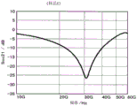
Fig. 5 is a diagram showing the transmission characteristics (Scc21 transmission characteristics) of the common mode component obtained for the common mode choke coil of sample 1 prepared in the experimental example to confirm the effect of the present invention.
Fig. 6 is a diagram showing the transmission characteristics (Sdd21 transmission characteristics) of the differential mode component obtained for the common mode choke coil according to sample 1.
Fig. 7 is a diagram showing the transmission characteristics (Scc21 transmission characteristics) of the common mode component obtained for the common mode choke coil of sample 2 prepared in the experimental example.
Fig. 8 is a diagram showing the transmission characteristics (Sdd21 transmission characteristics) of the differential mode component obtained for the common mode choke coil according to sample 2.
Fig. 9 is a diagram showing the transmission characteristics (Scc21 transmission characteristics) of the common mode component obtained for the common mode choke coil of sample 3 prepared in the experimental example.
Fig. 10 is a diagram showing the transmission characteristics (Sdd21 transmission characteristics) of the differential mode component obtained for the common mode choke coil according to sample 3.
Fig. 11 is a diagram showing the transmission characteristics (Scc21 transmission characteristics) of the common mode component obtained for the common mode choke coil of sample 4 prepared in the experimental example.
Fig. 12 is a diagram showing the transmission characteristics (Sdd21 transmission characteristics) of the differential mode component obtained for the common mode choke coil according to sample 4.
Fig. 13 is a diagram showing the transmission characteristics (Scc21 transmission characteristics) of the common mode component obtained for the common mode choke coil of sample 5 prepared in the experimental example.
Fig. 14 is a diagram showing the transmission characteristics (Sdd21 transmission characteristics) of the differential mode component obtained for the common mode choke coil according to sample 5.
Fig. 15 is a diagram showing the transmission characteristics (Scc21 transmission characteristics) of the common mode component obtained for the common mode choke coil of sample 6 prepared in the experimental example.
Fig. 16 is a diagram showing the transmission characteristics (Sdd21 transmission characteristics) of the differential mode component obtained for the common mode choke coil according to sample 6.
Fig. 17 is a plan view corresponding to fig. 2, in which a main portion of the common mode choke coil of sample 6 produced as a comparative example is exploded.
Description of the reference numerals
A common mode choke; a laminate; 3. 3a, 3b, 3c, 3d, 3e.. non-conductive layer; 5. a major face; 7. a side surface; 9. an end face; a first coil; a second coil; 13-16. 17. A coil conductor; 19-22. Connecting the end parts; 27. a via conductor; 29. a joint.
Detailed Description
A common mode choke coil 1 according to an embodiment of the present invention will be described with reference to fig. 1 to 4.
As shown in fig. 1, the common mode choke coil 1 includes a laminate 2 having a plurality of laminated non-conductive layers. Fig. 2 illustrates representative ones of the plurality of non-conductor layers 3a, 3b, 3c, 3d, and 3e. In the following, except for the case where the non-conductive layers are distinguished from each other as in the non-conductive layers 3a, 3b, 3c, 3d, and 3e shown in fig. 2, in the case of a general description of the non-conductive layers, the non-conductive layer is denoted by a reference numeral "3". The non-conductive layer 3 is made of a non-conductive material including, for example, glass and ceramic.
The laminate 2 is in the shape of a rectangular parallelepiped, and has: a first main surface 5 and a second main surface 6 extending in the extending direction of the non-conductor layer 3 and facing each other; a first side surface 7 and a second side surface 8 which are connected to each other and face each other between the first main surface 5 and the second main surface 6; and a first end surface 9 and a second end surface 10 which are connected between the first main surface 5 and the second main surface 6 and between the first side surface 7 and the second side surface 8, respectively, and face each other. The rectangular parallelepiped shape may be a shape obtained by rounding or chamfering the ridge portion and the corner portion, for example.
As shown in fig. 2 and 3, the common mode choke coil 1 includes a first coil 11 and a second coil 12 built in the laminated body 2. As shown in fig. 1, the common mode choke coil 1 includes: a first terminal electrode 13, a second terminal electrode 14, a third terminal electrode 15, and a fourth terminal electrode 16 are provided on the outer surface of the laminate 2. More specifically, the first terminal electrode 13 and the third terminal electrode 15 are provided on the first side surface 7, and the second terminal electrode 14 and the fourth terminal electrode 16 are provided on the second side surface 8, respectively, and have shapes symmetrical to the first terminal electrode 13 and the third terminal electrode 15.
As shown in fig. 2, the first terminal electrode 13 and the second terminal electrode 14 are electrically connected to the first end 11a and the second end 11b of the first coil 11, which are different from each other. The third terminal electrode 15 and the fourth terminal electrode 16 are electrically connected to the third terminal 12a and the fourth terminal 12b of the second coil 12, which are different from each other.
In the following description, the non-conductive layers 3a, 3b, 3c, 3d, and 3e are stacked in the order shown in fig. 2 from bottom to top.
Referring to fig. 2, the first coil 11 includes a first coil conductor 17 disposed along the interface between the non-conductor layers 3b and 3 c. The first coil 11 has a first lead conductor 19 and a second lead conductor 20 provided with a first end 11a and a second end 11b, respectively. The first lead conductor 19 includes: and a first connection end portion 23 connected to the first terminal electrode 13 at the outer surface of the laminate 2. The second lead conductor 20 includes: and a second connection end portion 24 connected to the second terminal electrode 14 at the outer surface of the laminate 2.
The first connection end portion 23 is arranged along an interface between the non-conductive layers 3a and 3b different from an interface between the non-conductive layers 3b and 3c on which the first coil conductor 17 is arranged. The first lead conductor 19 further includes: a first via conductor 27 connected to the first coil conductor 17 and penetrating the non-conductive layer 3b between the first coil conductor 17 and the first connection end 23 in the thickness direction; and a first connection portion 29 which is arranged along the interface between the non-conductor layers 3a and 3b on which the first connection end portion 23 is arranged, and which connects the first via conductor 27 and the first connection end portion 23. The first connecting portion 29 preferably has a shape extending linearly. This can reduce the inductance generated by the first connection portion 29, and can improve the high-frequency characteristics.
On the other hand, the second coil 12 also includes the same elements as those of the first coil 11, as described below.
The second coil 12 has a second coil conductor 18 disposed along the interface between the non-conductive layers 3c and 3 d. The second coil 12 has a third lead conductor 21 and a fourth lead conductor 22 that provide a third end 12a and a fourth end 12b, respectively. The third lead conductor 21 includes: and a third connection end portion 25 connected to the third terminal electrode 15 at the outer surface of the laminate 2. The fourth lead conductor 22 includes: and a fourth connection terminal 26 connected to the fourth terminal electrode 16 at the outer surface of the laminate 2.
The third connection end portion 25 is arranged along an interface between the non-conductive layers 3d and 3e different from an interface between the non-conductive layers 3c and 3d on which the second coil conductor 18 is arranged. The third lead conductor 21 further includes: a second through hole conductor 28 connected to the second coil conductor 18 and penetrating the non-conductor layer 3d located between the second coil conductor 18 and the third connection end portion 25 in the thickness direction; and a second connection portion 30 arranged along the interface between the non-conductor layers 3d and 3e on which the third connection end portion 25 is arranged, and connecting the second via conductor 28 and the third connection end portion 25. The second coupling portion 30 preferably has a linearly extending shape, similar to the second coupling portion 29 described above. This reduces the inductance generated by the second coupling section 30, thereby improving the high-frequency characteristics.
The common mode choke coil 1 is mounted with the second main surface 6 of the laminate 2 facing the mounting substrate. In the embodiment, for example, the dimension L in the longitudinal direction of the laminate 2 in which the first end face 9 and the second end face 10 face each other is 0.55mm or more and 0.75mm or less, the dimension W in the width direction of the first side face 7 and the second side face 8 face each other is 0.40mm or more and 0.60mm or less, and the dimension H in the height direction of the first main face 5 and the second main face 6 face each other is 0.20mm or more and 0.40mm or less.
As can be seen from fig. 2 and 3, the number of turns of each of the first coil conductor 17 and the second coil conductor 18 of the common mode choke coil 1 is preferably less than 2 turns.
The number of turns is defined as follows. The first coil conductor 17 and the second coil conductor 18 each have a portion extending in an arc shape. The first coil conductor 17 included in the first coil 11 will be described with reference to fig. 4. As shown in fig. 4, a tangent T is drawn along the outer periphery of the coil conductor 17 in order from the start end to the end of the coil conductor 17, and the phase of the tangent T rotated by 360 degrees is defined as 1 turn. In the coil conductor 17 shown in fig. 4, the tangent T is rotated by about 307 degrees, and thus can be defined as about 0.85 turns. The number of turns is also defined for the second coil conductor 18 provided in the second coil 12.
The smaller the number of turns of the first coil conductor 17 and the second coil conductor 18, the more the stray capacitance formed between the first coil 11 and the second coil 12 can be reduced, and therefore, the improvement of the high-frequency characteristics of the common mode choke coil 1 can be facilitated.
As clearly shown in fig. 3, in the common mode choke coil 1, when the first coil conductor 17 and the second coil conductor 18 are viewed in plan in the lamination direction of the laminated body 2, the first coil conductor 17 and the second coil conductor 18 preferably do not overlap each other except for a portion where they cross each other. That is, it is preferable that the first coil conductor 17 and the second coil conductor 18 do not have portions that overlap each other and are parallel in the same direction. This can reduce the stray capacitance formed between the first coil 11 and the second coil 12, and as a result, can contribute to improving the high-frequency characteristics of the common mode choke coil 1.
As can be seen from fig. 3, when the first coil conductor 17 and the second coil conductor 18 are viewed in plan in the lamination direction of the laminate 2, two portions are provided at which the first coil conductor 17 and the second coil conductor 18 intersect with each other. By setting the crossing portion to two or less portions in this way, the stray capacitance formed between the first coil conductor 17 and the second coil conductor 18 is reduced, which contributes to improvement of high-frequency characteristics.
The distance between the first coil conductor 17 and the second coil conductor 18 is preferably 6 μm or more and 26 μm or less. If the distance is less than 6 μm, the stray capacitance formed between the first coil conductor 17 and the second coil conductor 18 may increase to such an extent that the high-frequency characteristics are degraded. On the other hand, if the distance exceeds 26 μm, the coupling coefficient between the first coil 11 and the second coil 12 may decrease.
In fig. 2, the non-conductive layers 3a, 3b, 3c, 3d, and 3e are illustrated as single layers, but at least some of them may be formed of multiple layers. Therefore, for example, the distance between the first coil conductor 17 and the second coil conductor 18 may be adjusted by changing the thickness of a single layer of the non-conductive layer 3c or by changing the number of layers constituting the non-conductive layer 3 c.
The terminal electrodes 13 to 16 are formed from the first main surface 5 to the second main surface 6, but the width of each of the terminal electrodes 13 to 16 on the first side surface 7 or the second side surface 8 (in fig. 1, the width of the first terminal electrode 13 on the first side surface 7 is represented by "W1") is preferably 0.1mm or more and 0.25mm or less, and more preferably 0.15mm or more. If the width is less than 0.1mm, the fixing strength may be insufficient when the common mode choke coil 1 is mounted on the mounting substrate. On the other hand, if the width exceeds 0.25mm, the transmission characteristic of the common mode component of the common mode choke coil 1, that is, the peak position of Scc21 may be less than 30 GHz.
In fig. 1, the terminal electrodes 13 to 16 are each formed to have a portion extending to the first main surface 5. Although not shown in fig. 1, the terminal electrodes 13 to 16 are formed so that a part thereof extends in the same manner on the second main surface 6. The dimension E of such an extension is preferably 0.02mm or more and 0.2mm or less, and more preferably 0.17mm or less. If the dimension E is less than 0.02mm, there is a possibility that the fixing strength of the common mode choke coil 1 at the time of mounting on the mounting substrate is reduced. On the other hand, if the dimension E exceeds 0.2mm, the transmission characteristic of the common mode component of the common mode choke coil 1, that is, the peak position of Scc21 may be less than 30 GHz.
The line width of each of the first coil conductor 17 and the second coil conductor 18 is preferably 10 μm or more and 24 μm or less. If the line width is less than 10 μm, the dc resistance of the coil conductors 17 and 18 may be large. On the other hand, if the line width exceeds 24 μm, the stray capacitance formed between the first coil conductor 17 and the second coil conductor 18 may increase to such an extent that the high-frequency characteristics are degraded.
Next, a preferred method of manufacturing the common mode choke coil 1 will be described.
The following steps are performed to produce a glass ceramic sheet to be the non-conductive layer 3. Will K2O、B2O3And SiO2And if necessary, Al2O3The alloy is weighed to a predetermined ratio, placed in a platinum crucible, and heated to a temperature of 1500 to 1600 ℃ in a firing furnace to be melted. The glass material is obtained by rapidly cooling the melt.
The glass material includes, for example, a glass material containing at least K, B and Si in terms of K2O is 0.5 to 5 mass% and B is converted to B2O310 to 25 mass% and Si is converted to SiO270 to 85 mass% and Al is converted to Al2O30 to 5 mass% of% of the composition.
Then, the glass material is pulverized so that D50 (particle diameter corresponding to 50% of the cumulative percentage based on the volume) is about 1 to 3 μm to obtain a glass powder.
Then, alumina powder and quartz (SiO) each having a D50 value of 0.5 to 2.0 μm2) The powder is added to the above glass powder, and is put into a ball mill together with a PSZ medium, and an organic binder such as a polyvinyl butyral system, an organic solvent such as ethanol or toluene, and a plasticizer are put into the ball mill and mixed to obtain a glass ceramic slurry.
Next, the slurry is formed into a sheet having a thickness of 20 to 30 μm by a doctor blade method or the like, and the obtained sheet is punched into a rectangular shape, thereby obtaining a plurality of glass ceramic sheets.
The inorganic component contained in the glass ceramic sheet includes, for example, a dielectric glass material containing 60 to 66 mass% of a glass material, 34 to 37 mass% of quartz, and 0.5 to 4 mass% of alumina.
On the other hand, a conductive paste containing Ag as a conductive component for forming the first coil 11 and the second coil 12 is prepared.
Next, a through hole for disposing the through hole conductors 27 and 28 is provided in a predetermined glass ceramic sheet by, for example, laser irradiation. Then, by applying a conductive paste to a predetermined glass ceramic sheet by, for example, screen printing, via hole conductors 27 and 28 filled with the conductive paste are formed in the via holes, and coil conductors 17 and 18, connection end portions 23 to 26 constituting lead conductors 19 to 22, and connection portions 29 and 30 are formed in a patterned state.
Next, a plurality of glass ceramic sheets are laminated so as to obtain the lamination order of the non-conductor layers 3a to 3e shown in fig. 2. In this case, an appropriate number of glass ceramic sheets, to which no through-hole is provided and no conductive paste is applied, are stacked on the upper and lower sides of the stack of these glass ceramic sheets, as necessary.
Next, the laminated glass ceramic sheets were subjected to hot isostatic pressing at a temperature of 80 ℃ and a pressure of 100MPa to obtain a laminated block.
Next, the stacked block is cut by a cutter or the like and singulated into a stacked structure having a size capable of being a stacked body 2 provided in each common mode choke coil 1.
Next, the laminated structure obtained by the singulation is fired in a firing furnace at a temperature of 860 to 900 ℃ for 1 to 2 hours, for example, at a temperature of 880 ℃ for 1.5 hours, to obtain a laminated body 2.
Preferably, the fired laminate 2 is put into a rotary drum machine together with a medium and rotated, whereby the ridge portions and corner portions are rounded or chamfered.
Next, a conductive paste containing Ag and glass is applied to the portion of the laminate 2 from which the connection end portions 23 to 26 are drawn, and then the conductive paste is fired at a temperature of 810 ℃ for 1 minute, for example, to form base films for the terminal electrodes 13 to 16. The thickness of the base film is, for example, 5 μm. Next, a Ni film and an Sn film are sequentially formed on the base film by plating, for example. The thicknesses of these Ni film and Sn film are, for example, 3 μm and 3 μm, respectively.
As described above, the common mode choke coil 1 shown in fig. 1 is completed.
The common mode choke coil 1 is characterized in that when Sdd21, which is the transmission characteristic of a differential mode component, is measured at a frequency of 0.1GHz to 100GHz, the frequency of Sdd21 is-3 dB or less and is 30GHz or more, and when Scc21, which is the transmission characteristic of a common mode component, is measured at a frequency of 10GHz to 60GHz, the minimum frequency of Scc21 is 20GHz or more and the minimum value of Scc21 is-20 dB or less.
The common mode choke coil 1 preferably has a Scc21 of-10 dB or less when measured at a frequency of 25GHz to 35 GHz.
The frequency at which Sdd21 becomes-3 dB is preferably 40GHz or higher.
Experimental examples carried out to confirm the realizability of the common mode choke coil having the above-described characteristics and to confirm the effects of the present invention will be described below.
[ Experimental example ]
The following samples were prepared. Further, the dimensions of the laminate provided in the common mode choke coil according to each sample were set such that the longitudinal dimension L was 0.65mm, the width dimension W was 0.50mm, and the height dimension H was 0.30 mm. In the common mode choke coil according to each sample, the line width of each of the first coil conductor and the second coil conductor was set to 0.018 mm.
1. Sample 1 (example)
Referring to fig. 2, a common mode choke coil according to sample 1 was prepared, in which the number of turns of the first coil conductor 17 was 0.8, the number of turns of the second coil conductor 18 was 1, and the distance SG1 from the first coil conductor 17 to the side surfaces 7 and 8 and the end surface 10 was 0.025mm, and the distance SG2 from the second coil conductor 18 to the side surfaces 7 and 8 and the end surfaces 9 and 10 was 0.105 mm.
2. Sample 2 (example)
A common mode choke coil according to sample 2 was prepared in the same manner as in sample 1 except that the distance SG1 from the first coil conductor 17 to each of the side surfaces 7 and 8 and the end surface 10 was 0.045 mm.
3. Sample 3 (example)
A common mode choke coil according to sample 3 was prepared in the same manner as in sample 1 except that the distance SG1 from the first coil conductor 17 to each of the side surfaces 7 and 8 and the end surface 10 was 0.065 mm.
4. Sample 4 (example)
A common mode choke coil according to sample 4 was prepared in the same manner as in sample 1 except that the distance SG1 from the first coil conductor 17 to each of the side surfaces 7 and 8 and the end surface 10 was 0.085 mm.
5. Sample 5 (example)
A common mode choke coil according to sample 5 was prepared in the same manner as in sample 1 except that the distance SG1 from the first coil conductor 17 to each of the side surfaces 7 and 8 and the end surface 10 was 0.105 mm.
Fig. 17 is a view corresponding to fig. 2 showing sample 6 (comparative example) described below. In fig. 17, elements corresponding to those shown in fig. 2 are denoted by the same reference numerals.
6. Sample 6 (comparative example)
Referring to fig. 17, a common mode choke coil according to sample 6 was prepared in which the number of turns of the first coil conductor 17 was 2, the number of turns of the second coil conductor 18 was 2, the distance SG1 from the first coil conductor 17 to the side surfaces 7 and 8 and the end surfaces 9 and 10 was 0.045mm, and the distance SG2 from the second coil conductor 18 to the side surfaces 7 and 8 and the end surfaces 9 and 10 was 0.105 mm.
The transmission characteristics of the common mode component (Scc21 transmission characteristics) and the transmission characteristics of the differential mode component (Sdd21 transmission characteristics) were obtained for the common mode chokes of the above samples 1 to 6.
Fig. 5 and 6 show the Scc21 transmission characteristics and the Sdd21 transmission characteristics obtained for the common mode choke coil of sample 1, respectively.
Fig. 7 and 8 show the Scc21 transmission characteristics and the Sdd21 transmission characteristics obtained for the common mode choke coil of sample 2, respectively.
Fig. 9 and 10 show the Scc21 transmission characteristics and the Sdd21 transmission characteristics obtained for the common mode choke coil of sample 3, respectively.
Fig. 11 and 12 show the Scc21 transmission characteristics and the Sdd21 transmission characteristics obtained for the common mode choke coil of sample 4, respectively.
Fig. 13 and 14 show the Scc21 transmission characteristics and the Sdd21 transmission characteristics obtained for the common mode choke coil of sample 5, respectively.
Fig. 15 and 16 show the Scc21 transmission characteristics and the Sdd21 transmission characteristics obtained for the common mode choke coil of sample 6, respectively.
From the characteristic diagrams shown in fig. 5 and 6, the peak position, the minimum value (transmittance at the peak position), the value (transmittance) at 25GHz and the value (transmittance) at 35GHz of the Scc21 transmittance characteristic, and the value (transmittance) at 30GHz and the value (transmittance) at 40GHz of the Sdd21 transmittance characteristic were obtained for sample 1.
Similarly, for sample 2, sample 3, sample 4, sample 13, sample 14, sample 6, and samples 15, 16, fig. 7 and 8, and fig. 9 and 10, and fig. 11 and 14, respectively, the peak position and the minimum value (transmittance at the peak position), the value (transmittance) at 25GHz and the value (transmittance) at 35GHz, and the value (transmittance) at 30GHz and the value (transmittance) at 40GHz of the transmission characteristic Sdd21 were determined for Scc21, respectively, for sample 6, and Sdd21, respectively. These results are shown in table 1.
TABLE 1
TABLE 1

As is clear from fig. 6, 8, 10, 12, 14 and 16 showing the Sdd21 transmission characteristics, in samples 1 to 6, when the Sdd21 transmission characteristics were measured at a frequency of 0.1GHz or more and 100GHz or less, the Sdd21 transmission characteristics were 30GHz or more at a frequency of-3 dB or less. Therefore, according to samples 1 to 6, the differential mode signal can be transmitted without being attenuated in the high frequency region of 25GHz to 35 GHz.
On the other hand, as is clear from fig. 5, 7, 9, 11, 13, 15 and table 1 showing the Scc transmission characteristics, the minimum value of the Scc21 transmission characteristics was-20 dB or less in samples 1 to 6, but when the Scc21 transmission characteristics were measured at a frequency of 10GHz or more and 60GHz or less, the frequency at which the Scc21 transmission characteristics became minimum was 20GHz or more in samples 1 to 5, whereas the frequency at which the Scc21 transmission characteristics became minimum was 12.70GHz which was less than 20GHz in sample 6. Therefore, according to samples 1 to 5, the common mode noise component can be effectively attenuated in the high frequency region of 25GHz to 35 GHz. In contrast, in sample 6, the common mode noise component cannot be attenuated in the high frequency region of 25GHz to 35 GHz.
Further, as is clear from the values at 25GHz and 35GHz of the transmission characteristics of Scc21 shown in Table 1, in samples 1 to 5, the transmission characteristics of Scc21 were-10 dB or less when measured at frequencies of 25GHz to 35GHz inclusive. In contrast, in sample 6, the transmission characteristic of Scc21 exceeded-10 dB. As can be seen from this, according to samples 1 to 5, the common mode noise component can be effectively attenuated even in the high frequency region of 25GHz to 35 GHz.
As is clear from fig. 6, 8, 10, 12, 14, and 16 showing the transmission characteristics of Sdd21, samples 1 to 4 in examples 1 to 5 had transmission characteristics of Sdd21 of-3 dB or less and a frequency of 40GHz or more. Therefore, even in a high frequency region of 40GHz or more, the differential mode signal can be transmitted without being attenuated.
On the other hand, in sample 5, as is clear from the values at 40GHz of the Sdd21 transmission characteristics shown in table 1, the values at 40GHz of the Sdd21 transmission characteristics already became-4.11 dB, and the frequency at which the Sdd21 transmission characteristics became-3 dB or less was less than 40 GHz. This is presumably because, as described above, in sample 5, since the distance SG1 measured from the first coil conductor 17 and the distance SG2 measured from the second coil conductor 18 were both 0.105mm, when viewed in a plan view in the lamination direction of the laminate 2, the first coil conductor 17 and the second coil conductor 18 overlap each other in a large number of portions, and thus the stray capacitance adversely affecting the high-frequency characteristics was increased.
The present invention has been described in connection with the illustrated embodiments, but various other modifications are possible within the scope of the present invention.
For example, one coil conductor provided in at least one of the first coil and the second coil may be divided into two parts, the divided first part and second part may be arranged along a first interface and a second interface different from each other between the nonconductive layers, respectively, and the first part and the second part may be connected by a via conductor.
Claims (3)
1. A common mode choke coil is characterized by comprising:
a laminate having a plurality of laminated non-conductive layers, the non-conductive layers being made of a non-conductive material;
a first coil and a second coil which are built in the laminate;
a first terminal electrode and a second terminal electrode provided on an outer surface of the laminate and electrically connected to a first end and a second end of the first coil, respectively, which are different from each other; and
a third terminal electrode and a fourth terminal electrode provided on an outer surface of the laminate and electrically connected to a third terminal and a fourth terminal of the second coil, respectively,
when the Sdd21 transmission characteristic, which is the transmission characteristic of a differential mode component, is measured at a frequency of 0.1GHz or more and 100GHz or less, the Sdd21 transmission characteristic is such that the frequency at which-3 dB or less is 30GHz or more,
when Scc21 transmission characteristics, which are transmission characteristics of common mode components, are measured at frequencies of 10GHz to 60GHz, Scc21 transmission characteristics are measured at a frequency of 20GHz or higher,
the minimum value of the transmission characteristic of Scc21 is-20 dB or less.
2. A common mode choke according to claim 1,
the transmission characteristic of Scc21 is-10 dB or less when measured at a frequency of 25GHz or more and 35GHz or less.
3. A common mode choke according to claim 1 or 2,
the Sdd21 transmission characteristic is a frequency of 40GHz or higher at-3 dB or lower.
Applications Claiming Priority (2)
| Application Number | Priority Date | Filing Date | Title |
|---|---|---|---|
| JP2020017324A JP7163935B2 (en) | 2020-02-04 | 2020-02-04 | common mode choke coil |
| JP2020-017324 | 2020-02-04 |
Publications (2)
| Publication Number | Publication Date |
|---|---|
| CN113284696A true CN113284696A (en) | 2021-08-20 |
| CN113284696B CN113284696B (en) | 2023-04-18 |
Family
ID=77061817
Family Applications (1)
| Application Number | Title | Priority Date | Filing Date |
|---|---|---|---|
| CN202110148485.9A Active CN113284696B (en) | 2020-02-04 | 2021-02-03 | Common mode choke coil |
Country Status (4)
| Country | Link |
|---|---|
| US (1) | US20210241959A1 (en) |
| JP (1) | JP7163935B2 (en) |
| KR (1) | KR102444726B1 (en) |
| CN (1) | CN113284696B (en) |
Citations (26)
| Publication number | Priority date | Publication date | Assignee | Title |
|---|---|---|---|---|
| US4660014A (en) * | 1985-06-19 | 1987-04-21 | Jaycor | Electromagnetic pulse isolation transformer |
| US6246310B1 (en) * | 1998-11-19 | 2001-06-12 | Murata Manufacturing Co., Ltd | Noise suppressing apparatus |
| TW480827B (en) * | 1999-05-13 | 2002-03-21 | Nippon Electric Co | Self-tunable oscillator for oscillating signal synchronous with input signal |
| JP2006313946A (en) * | 2006-08-28 | 2006-11-16 | Tdk Corp | Thin film type common mode choke coil and common mode choke coil array |
| US20060291128A1 (en) * | 2005-06-24 | 2006-12-28 | Tdk Corporation | Surge absorption circuit |
| TWI274175B (en) * | 2005-11-07 | 2007-02-21 | Chunghwa Telecom Co Ltd | High precision frequency synchronizing system using GPS signal |
| US20090140829A1 (en) * | 2007-12-04 | 2009-06-04 | Nicklas Sodo | Filtering choke arrangement |
| JP2011119492A (en) * | 2009-12-04 | 2011-06-16 | Elmec Corp | Common mode filter |
| US20110273258A1 (en) * | 2010-05-05 | 2011-11-10 | Nxp B.V. | Integrated transformer |
| CN102568798A (en) * | 2012-02-23 | 2012-07-11 | 深圳顺络电子股份有限公司 | Sheet type common-mode choke row |
| US20140049350A1 (en) * | 2010-11-25 | 2014-02-20 | Cyntec Co., Ltd. | Method of producing an inductor with a high inductance |
| JP2014135674A (en) * | 2013-01-11 | 2014-07-24 | Matsue Elmec Corp | Common mode filter |
| US20140225698A1 (en) * | 2013-02-13 | 2014-08-14 | Nokia Corporation | Integrated transformer balun with enhanced common-mode rejection for radio frequency, microwave, and millimeter-wave integrated circuits |
| CN104170034A (en) * | 2012-03-16 | 2014-11-26 | 株式会社村田制作所 | Common mode choke coil |
| CN204045316U (en) * | 2011-11-04 | 2014-12-24 | 株式会社村田制作所 | Common mode choke and high-frequency electron device |
| CN104319075A (en) * | 2014-09-19 | 2015-01-28 | 南方电网科学研究院有限责任公司 | Connecting reactor for multi-level voltage source converter |
| CN104681233A (en) * | 2013-11-28 | 2015-06-03 | 卓英社有限公司 | Stack type common mode filter for high frequency |
| CN104737448A (en) * | 2012-10-19 | 2015-06-24 | 株式会社村田制作所 | Common mode filter |
| CN105590733A (en) * | 2014-11-10 | 2016-05-18 | 株式会社村田制作所 | Common mode choke coil |
| CN106486269A (en) * | 2015-08-26 | 2017-03-08 | 株式会社村田制作所 | Electronic unit |
| CN106877835A (en) * | 2015-09-25 | 2017-06-20 | 株式会社村田制作所 | Electronic unit |
| CN107809107A (en) * | 2016-09-08 | 2018-03-16 | 安世有限公司 | Inductive for static discharge |
| CN108573792A (en) * | 2017-03-07 | 2018-09-25 | 株式会社村田制作所 | Common mode choke |
| CN109887707A (en) * | 2017-11-27 | 2019-06-14 | 株式会社村田制作所 | Laminated coil parts |
| CN110120291A (en) * | 2018-02-07 | 2019-08-13 | 株式会社村田制作所 | Common mode choke coil |
| CN110349733A (en) * | 2018-04-02 | 2019-10-18 | 株式会社村田制作所 | Laminated coil element |
Family Cites Families (12)
| Publication number | Priority date | Publication date | Assignee | Title |
|---|---|---|---|---|
| JPH05326269A (en) * | 1992-05-20 | 1993-12-10 | Murata Mfg Co Ltd | Layered chip coil |
| JP3724405B2 (en) * | 2001-10-23 | 2005-12-07 | 株式会社村田製作所 | Common mode choke coil |
| EP1635363A1 (en) * | 2004-05-28 | 2006-03-15 | Matsushita Electric Industrial Co., Ltd. | Common mode noise filter |
| WO2006073029A1 (en) * | 2005-01-07 | 2006-07-13 | Murata Manufacturing Co., Ltd. | Electronic component and electronic component manufacturing method |
| JP4844045B2 (en) * | 2005-08-18 | 2011-12-21 | Tdk株式会社 | Electronic component and manufacturing method thereof |
| JP5073373B2 (en) * | 2007-06-08 | 2012-11-14 | Tdk株式会社 | Common mode choke coil |
| CN102982965B (en) * | 2011-09-02 | 2015-08-19 | 株式会社村田制作所 | Common mode choke coil and method for manufacturing the same |
| KR101968585B1 (en) * | 2016-02-05 | 2019-04-12 | 주식회사 아모텍 | Differential and common mode filter |
| JP6845540B2 (en) * | 2017-05-17 | 2021-03-17 | 国立大学法人信州大学 | Single layer thin film common mode filter |
| JP7044508B2 (en) * | 2017-09-29 | 2022-03-30 | 太陽誘電株式会社 | Magnetic coupling type coil parts |
| JP7032214B2 (en) * | 2018-04-02 | 2022-03-08 | 株式会社村田製作所 | Laminated coil parts |
| JP6879275B2 (en) * | 2017-11-29 | 2021-06-02 | 株式会社村田製作所 | Electronic components |
-
2020
- 2020-02-04 JP JP2020017324A patent/JP7163935B2/en active Active
-
2021
- 2021-02-01 KR KR1020210013972A patent/KR102444726B1/en active IP Right Grant
- 2021-02-02 US US17/165,712 patent/US20210241959A1/en active Granted
- 2021-02-03 CN CN202110148485.9A patent/CN113284696B/en active Active
Patent Citations (27)
| Publication number | Priority date | Publication date | Assignee | Title |
|---|---|---|---|---|
| US4660014A (en) * | 1985-06-19 | 1987-04-21 | Jaycor | Electromagnetic pulse isolation transformer |
| US6246310B1 (en) * | 1998-11-19 | 2001-06-12 | Murata Manufacturing Co., Ltd | Noise suppressing apparatus |
| TW480827B (en) * | 1999-05-13 | 2002-03-21 | Nippon Electric Co | Self-tunable oscillator for oscillating signal synchronous with input signal |
| US20060291128A1 (en) * | 2005-06-24 | 2006-12-28 | Tdk Corporation | Surge absorption circuit |
| TWI274175B (en) * | 2005-11-07 | 2007-02-21 | Chunghwa Telecom Co Ltd | High precision frequency synchronizing system using GPS signal |
| JP2006313946A (en) * | 2006-08-28 | 2006-11-16 | Tdk Corp | Thin film type common mode choke coil and common mode choke coil array |
| US20090140829A1 (en) * | 2007-12-04 | 2009-06-04 | Nicklas Sodo | Filtering choke arrangement |
| JP2011119492A (en) * | 2009-12-04 | 2011-06-16 | Elmec Corp | Common mode filter |
| US20110273258A1 (en) * | 2010-05-05 | 2011-11-10 | Nxp B.V. | Integrated transformer |
| US20140049350A1 (en) * | 2010-11-25 | 2014-02-20 | Cyntec Co., Ltd. | Method of producing an inductor with a high inductance |
| CN204045316U (en) * | 2011-11-04 | 2014-12-24 | 株式会社村田制作所 | Common mode choke and high-frequency electron device |
| CN102568798A (en) * | 2012-02-23 | 2012-07-11 | 深圳顺络电子股份有限公司 | Sheet type common-mode choke row |
| CN104170034A (en) * | 2012-03-16 | 2014-11-26 | 株式会社村田制作所 | Common mode choke coil |
| CN104737448A (en) * | 2012-10-19 | 2015-06-24 | 株式会社村田制作所 | Common mode filter |
| JP2014135674A (en) * | 2013-01-11 | 2014-07-24 | Matsue Elmec Corp | Common mode filter |
| US20140225698A1 (en) * | 2013-02-13 | 2014-08-14 | Nokia Corporation | Integrated transformer balun with enhanced common-mode rejection for radio frequency, microwave, and millimeter-wave integrated circuits |
| CN104681233A (en) * | 2013-11-28 | 2015-06-03 | 卓英社有限公司 | Stack type common mode filter for high frequency |
| CN104319075A (en) * | 2014-09-19 | 2015-01-28 | 南方电网科学研究院有限责任公司 | Connecting reactor for multi-level voltage source converter |
| CN105590733A (en) * | 2014-11-10 | 2016-05-18 | 株式会社村田制作所 | Common mode choke coil |
| CN106486269A (en) * | 2015-08-26 | 2017-03-08 | 株式会社村田制作所 | Electronic unit |
| CN106877835A (en) * | 2015-09-25 | 2017-06-20 | 株式会社村田制作所 | Electronic unit |
| CN107809107A (en) * | 2016-09-08 | 2018-03-16 | 安世有限公司 | Inductive for static discharge |
| CN108573792A (en) * | 2017-03-07 | 2018-09-25 | 株式会社村田制作所 | Common mode choke |
| CN208014475U (en) * | 2017-03-07 | 2018-10-26 | 株式会社村田制作所 | Common mode choke |
| CN109887707A (en) * | 2017-11-27 | 2019-06-14 | 株式会社村田制作所 | Laminated coil parts |
| CN110120291A (en) * | 2018-02-07 | 2019-08-13 | 株式会社村田制作所 | Common mode choke coil |
| CN110349733A (en) * | 2018-04-02 | 2019-10-18 | 株式会社村田制作所 | Laminated coil element |
Non-Patent Citations (2)
| Title |
|---|
| 何君;张铁军;熊伟;张波;和挺;沈京玲;: "基于聚酰亚胺基底的太赫兹滤波器" * |
| 周鹏: "新型GHz多模超宽带共模滤波器的研究与设计", 《中国优秀硕士学位论文全文数据库》 * |
Also Published As
| Publication number | Publication date |
|---|---|
| JP2021125534A (en) | 2021-08-30 |
| KR102444726B1 (en) | 2022-09-16 |
| CN113284696B (en) | 2023-04-18 |
| US20210241959A1 (en) | 2021-08-05 |
| KR20210099523A (en) | 2021-08-12 |
| JP7163935B2 (en) | 2022-11-01 |
Similar Documents
| Publication | Publication Date | Title |
|---|---|---|
| US7911295B2 (en) | Common mode noise filter | |
| US6294967B1 (en) | Laminated type dielectric filter | |
| US11587720B2 (en) | Multilayer coil component | |
| CN114068129B (en) | Common mode choke | |
| CN113223810B (en) | Common mode choke | |
| CN113223808B (en) | Common mode choke coil | |
| CN114068130B (en) | Common mode choke | |
| US11557416B2 (en) | Multilayer coil component | |
| CN113284696B (en) | Common mode choke coil | |
| CN113223811B (en) | Common mode choke coil | |
| CN114068128B (en) | Common mode choke | |
| JP7475946B2 (en) | Multilayer coil parts | |
| CN113223809B (en) | Common mode choke | |
| KR102373257B1 (en) | Common mode choke coil | |
| JPH08167523A (en) | Laminated inductor and manufacture thereof | |
| JP2002261504A (en) | Multilayer dielectric filter |
Legal Events
| Date | Code | Title | Description |
|---|---|---|---|
| PB01 | Publication | ||
| PB01 | Publication | ||
| SE01 | Entry into force of request for substantive examination | ||
| SE01 | Entry into force of request for substantive examination | ||
| GR01 | Patent grant | ||
| GR01 | Patent grant |