CN113271241A - Differential bus network - Google Patents
Differential bus network Download PDFInfo
- Publication number
- CN113271241A CN113271241A CN202110171373.5A CN202110171373A CN113271241A CN 113271241 A CN113271241 A CN 113271241A CN 202110171373 A CN202110171373 A CN 202110171373A CN 113271241 A CN113271241 A CN 113271241A
- Authority
- CN
- China
- Prior art keywords
- bus
- differential
- lines
- transmitter
- state
- Prior art date
- Legal status (The legal status is an assumption and is not a legal conclusion. Google has not performed a legal analysis and makes no representation as to the accuracy of the status listed.)
- Granted
Links
- 230000011664 signaling Effects 0.000 claims abstract description 56
- 230000005540 biological transmission Effects 0.000 claims abstract description 27
- 230000008878 coupling Effects 0.000 claims abstract description 20
- 238000010168 coupling process Methods 0.000 claims abstract description 20
- 238000005859 coupling reaction Methods 0.000 claims abstract description 20
- 230000002401 inhibitory effect Effects 0.000 claims abstract description 11
- 230000007704 transition Effects 0.000 claims description 16
- 238000000034 method Methods 0.000 claims description 15
- 238000013461 design Methods 0.000 claims description 12
- 238000011144 upstream manufacturing Methods 0.000 claims description 3
- 238000001514 detection method Methods 0.000 claims description 2
- 230000001629 suppression Effects 0.000 description 27
- 230000008859 change Effects 0.000 description 4
- 238000004891 communication Methods 0.000 description 4
- 238000010586 diagram Methods 0.000 description 3
- 239000000463 material Substances 0.000 description 2
- 238000012986 modification Methods 0.000 description 2
- 230000004048 modification Effects 0.000 description 2
- 230000009467 reduction Effects 0.000 description 2
- 230000001010 compromised effect Effects 0.000 description 1
- 239000004020 conductor Substances 0.000 description 1
- 230000000694 effects Effects 0.000 description 1
- 230000005672 electromagnetic field Effects 0.000 description 1
- 230000006872 improvement Effects 0.000 description 1
- 238000009434 installation Methods 0.000 description 1
- 238000004519 manufacturing process Methods 0.000 description 1
- 230000008569 process Effects 0.000 description 1
- 238000012545 processing Methods 0.000 description 1
- 230000004044 response Effects 0.000 description 1
Images


Classifications
-
- H—ELECTRICITY
- H04—ELECTRIC COMMUNICATION TECHNIQUE
- H04L—TRANSMISSION OF DIGITAL INFORMATION, e.g. TELEGRAPHIC COMMUNICATION
- H04L12/00—Data switching networks
- H04L12/28—Data switching networks characterised by path configuration, e.g. LAN [Local Area Networks] or WAN [Wide Area Networks]
- H04L12/40—Bus networks
- H04L12/40006—Architecture of a communication node
- H04L12/40013—Details regarding a bus controller
-
- H—ELECTRICITY
- H04—ELECTRIC COMMUNICATION TECHNIQUE
- H04L—TRANSMISSION OF DIGITAL INFORMATION, e.g. TELEGRAPHIC COMMUNICATION
- H04L12/00—Data switching networks
- H04L12/28—Data switching networks characterised by path configuration, e.g. LAN [Local Area Networks] or WAN [Wide Area Networks]
- H04L12/40—Bus networks
- H04L12/40006—Architecture of a communication node
- H04L12/40032—Details regarding a bus interface enhancer
-
- H—ELECTRICITY
- H04—ELECTRIC COMMUNICATION TECHNIQUE
- H04L—TRANSMISSION OF DIGITAL INFORMATION, e.g. TELEGRAPHIC COMMUNICATION
- H04L12/00—Data switching networks
- H04L12/28—Data switching networks characterised by path configuration, e.g. LAN [Local Area Networks] or WAN [Wide Area Networks]
- H04L12/40—Bus networks
- H04L12/40006—Architecture of a communication node
- H04L12/40039—Details regarding the setting of the power status of a node according to activity on the bus
-
- H—ELECTRICITY
- H04—ELECTRIC COMMUNICATION TECHNIQUE
- H04L—TRANSMISSION OF DIGITAL INFORMATION, e.g. TELEGRAPHIC COMMUNICATION
- H04L25/00—Baseband systems
- H04L25/02—Details ; arrangements for supplying electrical power along data transmission lines
- H04L25/08—Modifications for reducing interference; Modifications for reducing effects due to line faults ; Receiver end arrangements for detecting or overcoming line faults
- H04L25/085—Arrangements for reducing interference in line transmission systems, e.g. by differential transmission
-
- H—ELECTRICITY
- H04—ELECTRIC COMMUNICATION TECHNIQUE
- H04L—TRANSMISSION OF DIGITAL INFORMATION, e.g. TELEGRAPHIC COMMUNICATION
- H04L25/00—Baseband systems
- H04L25/38—Synchronous or start-stop systems, e.g. for Baudot code
- H04L25/40—Transmitting circuits; Receiving circuits
- H04L25/49—Transmitting circuits; Receiving circuits using code conversion at the transmitter; using predistortion; using insertion of idle bits for obtaining a desired frequency spectrum; using three or more amplitude levels ; Baseband coding techniques specific to data transmission systems
-
- H—ELECTRICITY
- H04—ELECTRIC COMMUNICATION TECHNIQUE
- H04L—TRANSMISSION OF DIGITAL INFORMATION, e.g. TELEGRAPHIC COMMUNICATION
- H04L12/00—Data switching networks
- H04L12/28—Data switching networks characterised by path configuration, e.g. LAN [Local Area Networks] or WAN [Wide Area Networks]
- H04L12/40—Bus networks
- H04L2012/40208—Bus networks characterized by the use of a particular bus standard
- H04L2012/40215—Controller Area Network CAN
-
- H—ELECTRICITY
- H04—ELECTRIC COMMUNICATION TECHNIQUE
- H04L—TRANSMISSION OF DIGITAL INFORMATION, e.g. TELEGRAPHIC COMMUNICATION
- H04L12/00—Data switching networks
- H04L12/28—Data switching networks characterised by path configuration, e.g. LAN [Local Area Networks] or WAN [Wide Area Networks]
- H04L12/40—Bus networks
- H04L2012/40208—Bus networks characterized by the use of a particular bus standard
- H04L2012/40241—Flexray
Landscapes
- Engineering & Computer Science (AREA)
- Computer Networks & Wireless Communication (AREA)
- Signal Processing (AREA)
- Power Engineering (AREA)
- Physics & Mathematics (AREA)
- Spectroscopy & Molecular Physics (AREA)
- Dc Digital Transmission (AREA)
Abstract
A differential bus network comprising: a bus comprising two bus lines; at least three nodes, each node comprising a transceiver comprising: a bus terminal for coupling to the two lines of a bus, respectively; a receiver arrangement configured to receive differential signaling from a bus end and to determine a digital receive signal based on the differential signaling; and a transmitter arrangement configured to apply differential signaling to the bus ends based on the digital transmission signal, the transmitter arrangement comprising a first transmitter configured to increase a potential difference between the lines of the bus to a first differential voltage state and maintain the first differential state, and an inhibiting element configured to decrease the potential difference between the lines of the bus towards a second differential voltage state, the transmitter arrangement further comprising a resistor coupled between the bus ends, the resistor configured to maintain at least the second differential voltage state.
Description
Technical Field
The present disclosure relates to a differential bus network. The present disclosure also relates to a general transceiver design for use in all nodes coupled to a differential bus network. The disclosure also relates to a kit of parts and a method for forming a differential bus network.
Background
A communication bus-based network comprising a pair of lines may require a certain resistance between the lines to enable differential signaling to be effectively provided over the bus lines.
Disclosure of Invention
According to a first aspect of the present disclosure there is provided a differential bus network comprising:
a bus comprising at least two bus lines;
at least three nodes, wherein each of the at least three nodes comprises:
a transceiver, comprising:
a bus terminal for coupling to the at least two lines of the bus, respectively;
a receiver arrangement configured to receive differential signaling from the bus end and to determine a digital receive signal based on the differential signaling; and
a transmitter arrangement configured to apply differential signaling to the bus ends based on a digital transmission signal, the transmitter arrangement comprising a first transmitter configured to increase a potential difference between the at least two lines of the bus to a first differential voltage state and maintain the first differential state, and an inhibiting element configured to decrease the potential difference between the at least two lines of the bus towards a second differential voltage state, the transmitter arrangement further comprising a resistor coupled between the bus ends, the resistor configured to at least maintain the second differential voltage state.
Thus, in one or more examples, the resistor coupled between the bus ends in each of the nodes is configured to perform the function of a CAN protocol defined termination resistor at each end of the differential bus, as the resistor will draw energy from the bus line to enable the provision of a second differential voltage state according to the first differential state in combination with the second transmitter element. Thus, there is no dedicated node pair of the differential bus network that includes termination resistors coupling the at least two bus lines together. Thus, the at least two lines of the bus of the differential bus network may be uncoupled except at the node.
In one or more embodiments, the bus comprises a controller area network, CAN, bus, and wherein the transceiver of each of the at least three nodes is configured to provide the digital receive signal to a CAN protocol controller and receive the digital transmit signal from the CAN protocol controller.
In one or more examples, the differential bus network includes a FlexRay differential bus network configured to operate at least partially according to a FlexRay protocol.
In one or more embodiments, the resistor comprises a discrete resistor coupled between the bus ends downstream of the transmitter arrangement and upstream of the receiver arrangement.
In one or more embodiments, the first differential state comprises providing a potential difference between the at least two bus lines greater than a threshold voltage to signal a bit of the digital transmission signal at a first logic level, and the second differential state comprises providing a substantially zero potential difference between the at least two bus lines less than the threshold voltage to signal a bit at a second logic level different from the first logic level.
In one or more embodiments, the transceiver is configured to provide the differential signaling representing the first logic level by enabling the first transmitter and configured to provide the differential signaling representing the second logic level by partially disabling the first transmitter.
In one or more embodiments, the transceiver includes a throttle controller configured to receive the digital transmission signal and configured to enable the throttling element for a predetermined time upon detecting a transition between the first logic level and the second logic level in the digital transmission signal requiring a transition from the first differential state to the second differential state.
In one or more examples, at the end of a predetermined time, the suppression controller is configured to deactivate the suppression element, e.g., until a next transition between logic states in the digital transmission signal requiring a transition from the first differential state to the second differential state.
In one or more embodiments, the inhibiting element is configured to reduce the potential difference between the at least two lines of the bus towards the second differential voltage state by applying to the at least two bus lines a potential difference of opposite polarity to a potential difference applied by a first transmitter to achieve the first differential voltage state, the transmitter arrangement being configured to deactivate the inhibiting element when the second differential state is reached.
In one or more examples, the second transmitter may be disabled based on detecting that the second differential state is reached. Thus, a sensor may be provided to sense a potential difference between the at least two bus lines.
In one or more embodiments, each node includes a controller including a CAN protocol controller to implement a CAN-based protocol in the network, the controller coupled to the transceiver through at least a first connection to provide the digital transmit signal to the transceiver and coupled to the transceiver through a second connection to receive the digital receive signal from the transceiver.
In one or more embodiments, the resistance of the resistor in ohms is at least 50 times the number of the at least three nodes. In one or more examples, the resistance of the resistor may be 45 times or 50 times greater than a maximum number of nodes to which the bus of the network is configured to couple. In one or more examples, the resistor may have a resistance greater than 50 ohms, or greater than 100 ohms, or greater than 200 ohms, or greater than 1000 ohms. In one or more examples, the configuration of the differential bus network is defined by a protocol, and wherein the protocol defines a minimum impedance of the bus, and wherein the resistance of the resistor may be greater than the minimum impedance of the bus multiplied by one of: a number of at least three nodes or a maximum number of nodes to which the bus of the network is configured to be coupled.
In one or more embodiments, the network includes only the at least three nodes.
In one or more embodiments, the bus includes two lines.
According to a second aspect of the present disclosure there is provided a kit of parts for forming a differential bus network, the kit comprising:
a bus comprising at least two bus lines;
at least three nodes, wherein each of the at least three nodes comprises:
a bus terminal for coupling to the at least two lines of the bus, respectively;
a transceiver, comprising:
a receiver arrangement configured to receive differential signaling from the bus end and to determine a digital receive signal based on the differential signaling; and
a transmitter arrangement configured to apply differential signaling to the bus ends based on a digital transmission signal, the transmitter arrangement comprising a first transmitter element configured to increase a potential difference between the at least two lines of the bus to a first differential voltage state and maintain the first differential state, and a second transmitter configured to decrease the potential difference between the at least two lines of the bus towards a second differential voltage state, the transmitter arrangement further comprising a resistor coupled between the bus ends, the resistor configured to at least maintain the second differential voltage state.
According to a third aspect of the present disclosure there is provided a method of forming a differential bus network, the method comprising:
providing a bus comprising at least two bus lines;
coupling at least three nodes to the bus, wherein each of the at least three nodes has a bus end for coupling to the at least two lines of the bus, respectively, and a general transceiver design for a transceiver, the transceiver comprising:
a receiver arrangement configured to receive differential signaling from the bus end and to determine a digital receive signal based on the differential signaling; and
a transmitter arrangement configured to apply differential signaling to the bus ends based on a digital transmission signal, the transmitter arrangement comprising a first transmitter element configured to increase a potential difference between the at least two lines of the bus to a first differential voltage state and maintain the first differential state, and a second transmitter configured to decrease the potential difference between the at least two lines of the bus towards a second differential voltage state, the transmitter arrangement further comprising a resistor coupled between the bus ends, the resistor configured to at least maintain the second differential voltage state.
In one or more embodiments, the method includes coupling respective controllers to one or more of the transceivers of the at least three nodes, each respective controller configured to provide the digital transmit signal to the transceiver and receive the digital receive signal from the transceiver.
According to a fourth aspect of the present disclosure, there is provided an electronic device comprising the differential bus network of the first aspect.
While the disclosure is susceptible to various modifications and alternative forms, specifics thereof have been shown by way of example in the drawings and will be described in detail. However, it is to be understood that other embodiments beyond the specific embodiments described are possible. The intention is to cover all modifications, equivalents, and alternatives falling within the spirit and scope of the appended claims.
The above discussion is not intended to represent each example embodiment, or every implementation, within the scope of the present or future claim sets. The figures and the detailed description that follow further illustrate various example embodiments. Various example embodiments may be more completely understood in consideration of the following detailed description in connection with the accompanying drawings.
Drawings
One or more embodiments will now be described, by way of example only, with reference to the accompanying drawings, in which:
FIG. 1 illustrates an example differential bus network including a controller area network;
FIG. 2 illustrates a practical example of a differential bus network including a controller area network;
FIG. 3 illustrates an example embodiment of a differential bus network according to this disclosure;
FIG. 4 illustrates a transceiver of one of the nodes of an embodiment of a differential bus network;
FIG. 5 illustrates a timing diagram showing voltages on a bus line in response to differential signaling applied thereto based on a digital transmission signal;
FIG. 6 shows a node of a network comprising a transceiver and a controller coupled to the transceiver; and
fig. 7 illustrates an example flow diagram of a method of the present disclosure.
Detailed Description
A differential bus network includes a network in which nodes of the network are coupled by a common physical medium that includes a bus. The bus provides a medium through which nodes can communicate. In the case of a differential bus, the bus typically includes two conductors or lines, such as twisted pair cables. Signalling on the bus is provided by applying a first voltage to one of the lines and a second voltage, typically of opposite polarity, to the other line. Data is represented by the voltage difference between the lines of the bus, and thus, the signaling is referred to as differential signaling. This differential signal is used to avoid electromagnetic emissions to the environment. If the signals carried by the two bus lines are of the same shape but of opposite polarity, the electromagnetic fields of the two lines will compensate each other in an ideal manner and thus not be emitted to the environment, and any interference absorbed by the lines will normally be absorbed by the two lines, so that the interference is cancelled when the voltage difference between the lines is determined.
Common differential bus networks include Controller Area Networks (CAN) or FlexRay networks. Example fig. 1 illustrates an example CAN network. Buses are commonly used in automotive and industrial automation applications. The CAN bus standard is described in the ISO11898 standard. When the network topology is properly terminated, the CAN bus CAN support bit rates up to 1Mb/s in the classical CAN case and up to 5Mbps or 8Mbps in the CAN FD (defined in ISO 11898-2:2016) case.
Fig. 1 shows a CAN bus 101 comprising a first line 102 and a second line 103. The network comprises a plurality of nodes, shown as n nodes, including a first node 104, a second node 105, a third node 106, an n-1 node 107 and an nth node. Each node is coupled to a first line 102, referred to as a CANH line, and a second line 103, referred to as a CANL line, to provide differential signaling to and receive differential signaling from the bus.
The CAN standard requires that the CANH and CANL lines 102, 103 are coupled together via termination resistors 109, 110, terminating the bus lines 102, 103 at each end of the bus. Terminals are shown at the first node 104 and the nth node 108. Termination resistors typically comprise 120 ohms because they represent the typical line impedance of a twisted pair cable, and therefore, the outermost end of the cable is "terminated" with a typical impedance to avoid signal reflections. As a result, the two end nodes 104, 108 are "specially equipped" nodes that differ from other network nodes in that they carry a 120 ohm termination resistor inside.
The theoretical speed of the CAN network CAN only be met if there is a suitable termination resistance (120 ohms) at the end nodes 104, 108 and the node without the termination resistor is connected to the main cable via stubs 111, 112, 113 connecting the nodes to the main cable length of the bus 101. The stub typically needs to be short to avoid long time reflections from the open end of the cable.
Example fig. 2 shows an example CAN network 200 including a two-wire bus (shown as a single wire in this example) in a real implementation with nodes 201 and 211. Although in the CAN network of fig. 1 the end nodes are easily identifiable, in the example of fig. 2 the presence of a large number of branches and stubs makes the ends less easily identifiable. In this example, nodes 207 and 210 are designated as termination nodes, and therefore include termination resistors that couple the two lines of the bus together.
When any of the nodes 201 and 211 start to transmit data, reflections in the network 200 will cause signal interference depending on the physical location of the transmitting node with respect to the nodes 207, 210 and the termination resistors at the cable branches. Using appropriate bus termination resistors can only avoid signal reflections under ideal conditions, which are true point-to-point connections of two nodes at the bus ends, or as an approximation a very linear bus has more nodes but very short stubs, similar to that shown in fig. 1.
As can be seen by comparing fig. 1 and 2, there are more nodes connected within the actual system and there is no longer a distinct start or end of the ideal cable in such topologies. Therefore, it is problematic to require the placement of termination resistors 109, 110 according to the current CAN standard.
The termination resistor typically performs two functions. They reduce signal reflections and are used to dissipate bus energy when transitioning between differential signaling that produces a high potential difference between bus lines and differential signaling that requires a low or zero potential difference between bus lines. The termination resistors therefore need to draw energy from the bus within a reasonable time to ensure that the different states represented by the signaling can be distinguished from each other within a reasonable time before transitioning to the next differential signaling bit.
Each node 104 and 108 generally includes a transceiver and a controller. A transceiver is a device comprising a transmitter arrangement and a receiver arrangement. Transmitter arrangements typically convert a digital transmission data stream into differential analog signals that can be communicated over a bus. The receiver arrangement is configured to convert the differential analog signal back into a digital receive data stream. Digital transmission data is received from an associated controller through a transceiver. The digital reception data is communicated to the controller by a receiver arrangement of the transceiver. The controller may include a protocol controller that implements rules of a protocol to send and receive data between nodes.
Example fig. 3 illustrates an example differential bus network 300 according to an embodiment of this disclosure. Example fig. 3 shows a differential bus network 300 comprising a bus 301 with at least two bus lines 302, 303. In the differential bus network 300 of the present disclosure, each node 304-308 in the network has a general purpose transceiver design involving the presence of resistors coupling the bus lines 302, 303 together. In some instances, it may be advantageous to use a general purpose transceiver design in a differential bus network.
As a conceptual implementation, the network 300 includes at least three nodes, specifically n nodes 304 and 308, in this example, where n ≧ 3. Thus, the example network 300 includes only the at least three nodes, such that the only nodes in the network are nodes with a common transceiver design. Referring to the example figures 3 and 4, each of the at least three nodes 304, 308 comprises a general purpose transceiver design involving bus terminals 402, 403 comprising at least two lines 302, 303 for coupling to a bus 301, respectively. The versatility of the transceiver of each node also relates to including a receiver arrangement 404, said receiver arrangement 404 being configured to receive differential signaling from the bus ends 402, 403 and to determine a digital receive signal based on said differential signaling. The digital receive signal may be provided to a controller (not shown) via receive output 405. The transceiver 400 additionally comprises a transmitter arrangement 406 configured to apply differential signaling to the bus ends 402, 403 based on a digital transmission signal, which may be received from a transmission input 407 from a controller (not shown).
In an example, the transmitter arrangement 406 comprises a first transmitter 408 configured to increase a potential difference between at least two lines 302, 303 of the bus to a first differential voltage state and maintain the first differential state. The transmitter arrangement further comprises a suppression element 409 configured to reduce the potential difference between the at least two lines 302, 303 of the bus towards the second differential voltage state. The suppression element 409 may be considered to comprise a dynamic "termination" resistor, as the suppression element may be configured to be selectively enabled to reduce the potential difference between the bus lines. The transmitter arrangement 406 further comprises said resistor coupled between the bus ends 402, 403 and configured to maintain at least a second differential voltage state. The use of the inhibiting element 409 of a potential difference that actively drives the bus toward the second differential voltage state may provide a sharper transition (i.e., a transition at a greater rate) between the first differential voltage state and the second differential voltage state. The suppression element 409 may be switchable such that it may be enabled when signaling requires adoption of the second differential voltage state from the first differential voltage state. Resistor 410 may be used to draw any remaining energy or other voltage disturbances from the bus lines to maintain the second differential voltage state.
Thus, in one or more examples, the resistor 410 coupled between the bus ends in each node is configured to perform the function of a termination resistor as defined by the CAN protocol at each end of the differential bus, as the resistor draws energy from the bus lines to enable the second differential voltage state to be provided from the first differential state in conjunction with the suppression element 409. Thus, when the suppression elements are enabled, it can be seen as facilitating a reduction in the voltage difference between the bus lines 302, 303, and once the suppression elements are disabled, the resistors of each transceiver will continue to be used to draw any energy in the bus to maintain the second differential level. Thus, there is no dedicated node pair of the differential bus network that includes termination resistors coupling the at least two bus lines together. Thus, the at least two lines 302, 303 of the bus of the differential bus network may be uncoupled except at nodes 304-308, where they are coupled by the resistor 410.
In one or more examples, a CAN transceiver providing such a design may avoid a system designer having to place two termination resistors in selected nodes (i.e., those at opposite ends of the bus), which makes these nodes "dedicated nodes". In fact, from a bus cable topology perspective, the location of the dedicated node may be physically located in an undesirable location. This imposes design limitations on the system designer.
Furthermore, when the network (as shown in fig. 1) requires so-called dedicated nodes, it is more difficult to use standard node designs in different networks, since on one network the nodes may need to comprise termination resistors 109, 110, but in another network they are not. This can lead to node variation, thereby increasing cost.
An open bus line near one of the nodes 104, 108 may cause a loss in one of the termination resistors 109, 110. This will change the bus impedance drastically and the overall bus communication between any of the nodes will be compromised by only a single bus fault.
In one or more instances, it may be advantageous to provide a general transceiver design that includes resistors between bus ends.
Thus, the resistor provides a resistance to draw energy from the bus line regardless of the operating state of the transmitter arrangement or the receiver arrangement. Since the suppression element transmitter 409 acts like a dynamic termination resistance to suppress ringing in the bus, the passive resistors 410 of all nodes 304-308 in parallel may be allowed to be above the maximum DC bus resistance 65 ohms specified in the ISO 11898-2 standard, but it may be desirable that the resistance should not be below the specified minimum DC bus resistance 50 ohms. Thus, where n is the maximum number of network nodes coupled to the communication bus, the value of the resistor 410 may be greater than (50 Ω n). As an example, an actual CAN network in an automotive setting assumes a maximum number of nodes of 32. This will result in a minimum resistance of 50 x 32-1.6 kilo ohms for resistor 410. As another example, if the exact number of nodes n in the network is fixed, the resistance of resistor 410 may be x n, where x is between 50 Ω and 70 Ω, and optionally 60 Ω.
In one or more examples, the bus 301 comprises a controller area network, CAN, bus, and wherein the transceiver 400 of each of the at least three nodes is configured to provide a digital receive signal to a CAN protocol controller 601 and receive a digital transmit signal from the CAN protocol controller (as shown in fig. 6). Although the examples herein refer to a CAN bus network, in other examples, the differential bus network may comprise a FlexRay differential bus network operating at least in part according to a FlexRay protocol.
In this and other examples, the resistor 410 comprises a discrete resistor coupled between the bus ends 402, 403 downstream of the transmitter arrangement 406 (i.e., on the output side of the transmitter arrangement 406) and upstream of the receiver arrangement 404 (i.e., on the input side of the receiver arrangement 404). It should be appreciated that the resistor 410 may or may not be physically coupled to the bus end, and may also be spaced apart from the bus end coupled to the bus line. For example, as shown in FIG. 4, the ends of the bus ends 402, 403 are spaced apart from the location where the resistor 410 couples the bus ends together. In some examples, the resistor 410 is easily removable so that its value can be changed to suit the number of nodes to be installed in the network. Thus, the resistor may be configured to snap into a holder in which the resistor is coupled with the bus end. In other examples, the transceiver 400 may include connectors for removably connecting resistors to the bus ends 402, 403.
Example fig. 5 shows a timing diagram showing the change in voltage of a transmission signal over time at 501. The differential bus voltage over time on the two bus lines is shown at 502. A digital receive signal that may be derived from the differential signaling at 502 is shown at 503. The dashed line represents the signal without the use of the suppression element 409 and the solid line represents the signal with the use of the suppression element 409.
During period 504, the digital transmit signal is logic high. In this example, a logic high is represented by the second differential state, so the differential signaling at 502 provides a zero potential difference between the first line and the second line of the bus, which is shown as the lines being at one and thus appearing to be one line. The digital receive signal is shown as detecting a logic high state because the differential signal is below a threshold value that the receiver is arranged to distinguish between the first differential state and the second differential state. At period 505, the digital transmit signal is logic low. In this example, a logic low is represented by a first differential state, so at 502, the first transmitter 408 drives the bus lines to provide differential signaling that provides a non-zero potential difference between the first and second lines of the bus. This is shown as lines 506 and 507 being separated, showing the voltage difference on the lines. Line 506 shows the potential of the CANH line, and line 507 shows the potential of the CANL line. The first transmitter 408 drives the bus lines relatively quickly to a first differential state and the receiver arrangement shows in trace 503 that a logic low state is detected upon passing a threshold (or a second threshold) used by the receiver to distinguish the first differential state from the second differential state.
During period 508, the digital transmission signal is logic high and thus requires differential signaling to transition from a first differential state to a second differential state, which includes a reduction in the potential difference between the lines of the bus. The suppressing element 409 is used to actively drive the bus line to a lower potential difference and thus the line 509 shows a relatively fast change from the first differential state to the second differential state. The transmitter 409 (or more generally, the suppression element) may be considered to act as a dynamic termination resistor when driving the bus voltage to a retrograde (receptive) or second differential state. The digital receive signal in trace 503 is shown detecting a differential signaling indicating a logic high state at time 510. The dashed line 511 shows the change of differential signaling from the first to the second differential state without the use of suppressing elements, e.g. in the network of fig. 1 the termination resistors 109, 110 instead enable the energy to be drawn from the bus lines. It will be appreciated that it takes longer for the potential difference between the bus lines to drop to the second differential state, so the receiver arrangement detects at a later time 512 that the differential signaling indicates a logic high state. Thus, the use of the suppression element 409 and the universal resistor 410 may provide a node that can communicate more efficiently.
In summary, the first differential state may include providing a potential difference between at least two bus lines, shown by traces 502, at time 505. The potential difference is greater than the threshold voltage and therefore it signals a bit of the digital transmission signal comprising a first logic level of logic low. The second differential state may comprise providing a smaller potential difference, in this example a substantially zero potential difference between the at least two bus lines. The potential difference is less than a threshold voltage and signals a bit of a second logic level comprising a logic high level.
Returning to fig. 4, the emitter arrangement 406 may comprise an suppression controller 411 coupled with a suppression element 409. The suppression controller 411 may be configured to enable the suppression element 409 (from a disabled or low power state) based on when differential signaling requires a transition from a first differential state to a second differential state. In one or more examples, the suppression controller 411 is configured to receive the digital transmission signal via branch 412 and is configured to enable the suppression element 409 for a predetermined time when a transition from the first differential state to the second differential state is required upon detection of a transition (e.g., a logic low to a logic high) between a first logic level and a second logic level in the digital transmission signal. The suppression element 409 may take the form of a feed forward signal improvement transceiver. It is known how fast the inhibit element 409 can drive the bus to the second differential state, and hence the enabling of the predetermined time period may provide a convenient way of applying differential signalling to the bus. In one or more examples, at the end of the predetermined time, the suppression controller 411 is configured to deactivate the suppression element 409, e.g., until a next transition between logic states in the digital transmission signal that requires a transition from the first differential state to the second differential state. The predetermined time should be shorter than the bit time of the logic level and shorter than the time required for the resistor 410 to draw energy from the bus.
It should be appreciated that in other examples, the inhibiting element 409 may be disabled based on detecting that the second differential state is being reached. Thus, a sensor (not shown) may be provided at the bus end to sense a potential difference between at least two bus lines.
In this and other examples, the inhibiting element 409 is configured to reduce the potential difference between the at least two lines of the bus towards the second differential voltage state by applying to the at least two bus lines a potential difference of opposite polarity to the potential difference applied by the first transmitter 408 to achieve the first differential voltage state. The transmitter arrangement 406 may be configured to deactivate the inhibiting element, for example, when the second differential state is reached or reached within a predetermined time using the sensor. The suppression element 409 may include other emitters. The emitters may be provided by an arrangement of transistors, as known to those skilled in the art. In other examples not shown herein, the suppression elements may include other resistors that may be switched to couple together or disconnect from the bus lines.
Thus, in one or more examples, the transmitter arrangement is configured to signal a transition from the second logic level to the first logic level (logic low) by enabling the first transmitter 408 to provide a potential between the bus lines as shown at 506, 507 and by not enabling the suppression element. Thus, the first transmitter 408 provides differential signaling to achieve and maintain a first differential state of the effect of the resistor 410, which passively draws energy from the bus. Additionally, in one or more examples, the transmitter arrangement is configured to signal a transition from the first logic level to the second logic level (logic high) by disabling the first transmitter 408 and by enabling the suppression element 409 for a predetermined time. The inhibit element 409 may then be disabled before the end of the bit time of the second logic level.
It should be appreciated that to maintain the first logic level during the next bit time, the first transmitter 408 remains enabled. It will also be appreciated that to maintain the second logic level during the next bit time, the first transmitter 408 remains in the disabled state, and because the second differential state has been achieved, the inhibit element 409 need not be enabled.
Example fig. 6 shows a CAN node 600 and the same reference numerals as used in fig. 4 have been used for the same components. Fig. 6 shows a controller 601 coupled to the CAN transceiver 400 by a first connection and a second connection that couple the transmit input 407 and the receive output 405, respectively, to convey digital transmit signals and digital receive signals between the controller 601 and the transceiver 400.
The controller 601 includes a protocol controller 602 that implements a CAN-based protocol. It should be appreciated that references to the CAN protocol may refer to the original CAN protocol or extensions thereof, such as CAN FD (ISO11898-1:2015) and proposed CAN XL.
It should be appreciated that the network of fig. 3 may be provided in an uncoupled form for installation in a device such as an automobile or other machine. Thus, a set of components may be provided for forming a differential bus network. The kit includes a bus comprising at least two bus lines, which may be in the form of a wire harness for routing around the vehicle. The set may comprise at least three nodes, wherein each of the at least three nodes comprises a transceiver comprising a bus end for coupling to the at least two lines of the bus, respectively, and a receiver arrangement configured to receive differential signaling from the bus ends and to determine a digital receive signal based on the differential signaling; and a transmitter arrangement configured to apply differential signaling to the bus ends based on a digital transmission signal, the transmitter arrangement comprising a first transmitter element configured to increase a potential difference between the at least two lines of the bus to a first differential voltage state and maintain the first differential state, and a second transmitter configured to decrease the potential difference between the at least two lines of the bus towards a second differential voltage state, the transmitter arrangement further comprising a resistor coupled between the bus ends, the resistor configured to at least maintain the second differential voltage state.
The kit may further include one or more controllers 601 for coupling with the transceiver 400.
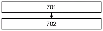
FIG. 7 illustrates an example method of forming a differential bus network, the method comprising:
providing 701 a bus comprising at least two bus lines;
coupling 702 at least three nodes to the bus, wherein each of the at least three nodes comprises a general transceiver design involving each transceiver comprising a bus end for coupling to the at least two lines of the bus, respectively; and
a receiver arrangement configured to receive differential signaling from the bus end and to determine a digital receive signal based on the differential signaling; and
a transmitter arrangement configured to apply differential signaling to the bus ends based on a digital transmission signal, the transmitter arrangement comprising a first transmitter element configured to increase a potential difference between the at least two lines of the bus to a first differential voltage state and maintain the first differential state, and a second transmitter configured to decrease the potential difference between the at least two lines of the bus towards a second differential voltage state, the transmitter arrangement further comprising a resistor coupled between the bus ends, the resistor configured to at least maintain the second differential voltage state.
When forming a differential bus network, pre-established protocols may be followed, wherein the protocols may define one or more of physical specifications, minimum performance requirements, timing requirements, voltage level requirements, message frame formats, and other factors for the components of the differential bus network. In particular, the protocol may define a minimum impedance of a bus, and the method may include determining the resistance of the resistor of each of the at least three nodes, wherein the resistance of the resistor in ohms may be greater than the minimum impedance of the bus multiplied by one of: a number of at least three nodes or a maximum number of nodes to which the bus of the network is configured to be coupled. Thus, once the resistance is determined, the node may be configured such that the resistor has the determined resistance. It will be appreciated that when a node is added to the bus, the resistors are connected in parallel, which reduces the overall impedance of the bus, so accordingly, the network may limit the number of nodes permitted to couple with the bus.
The method may additionally comprise coupling a controller 601 implementing a communication protocol, such as CAN or FlexRay, to one or each of the transceivers.
The instructions in the above figures and/or the flowchart steps may be executed in any order, unless a specific order is explicitly stated. Moreover, those skilled in the art will recognize that while one example instruction set/method has been discussed, the materials in this specification can be combined in various ways to produce yet other examples, and should be understood within the context provided by this detailed description.
In some example embodiments, the instruction sets/method steps described above are implemented as functions and software instructions embodied as a set of executable instructions that are implemented on a computer or machine programmed and controlled with the executable instructions. Such instructions are loaded for execution on a processor (e.g., CPU or CPUs). The term processor includes microprocessors, microcontrollers, processor modules or subsystems (including one or more microprocessors or microcontrollers), or other control or computing devices. A processor may refer to a single component or a plurality of components.
In other examples, the sets of instructions/methods illustrated herein, as well as data and instructions associated therewith, are stored in respective storage devices implemented as one or more non-transitory machine or computer-readable or computer-usable storage media. Such computer-readable or computer-usable storage media are considered to be part of an article (or article of manufacture). An article or article may refer to any manufactured component or components. Non-transitory machine or computer usable media as defined herein do not include signals, but such media may be capable of receiving and processing information from signals and/or other transitory media.
Example embodiments of the materials discussed in this specification can be implemented in whole or in part by a network, computer, or data-based device and/or service. These may include clouds, the internet, intranets, mobile devices, desktops, processors, look-up tables, microcontrollers, consumer devices, infrastructure, or other enabled devices and services. As used herein and in the claims, the following non-exclusive definitions are provided.
In one example, one or more instructions or steps discussed herein are automated. The term automated or automatic (and similar variations thereof) means that the operation of a device, system, and/or process is controlled using a computer and/or mechanical/electrical means without the need for human intervention, observation, effort, and/or decision-making.
It is to be understood that any components that are said to be coupled may be directly or indirectly coupled or connected. In the case of indirect coupling, additional components may be disposed between the two components that are said to be coupled.
In this specification, example embodiments have been presented in terms of selected sets of details. However, those of ordinary skill in the art will understand that many other example embodiments may be practiced that include different selected sets of these details. It is intended that the appended claims cover all possible example embodiments.
Claims (10)
1. A differential bus network, comprising:
a bus comprising at least two bus lines;
at least three nodes, wherein each of the at least three nodes comprises:
a transceiver, comprising:
a bus terminal for coupling to the at least two lines of the bus, respectively;
a receiver arrangement configured to receive differential signaling from the bus end and to determine a digital receive signal based on the differential signaling; and
a transmitter arrangement configured to apply differential signaling to the bus ends based on a digital transmission signal, the transmitter arrangement comprising a first transmitter configured to increase a potential difference between the at least two lines of the bus to a first differential voltage state and maintain the first differential state, and an inhibiting element configured to decrease the potential difference between the at least two lines of the bus towards a second differential voltage state, the transmitter arrangement further comprising a resistor coupled between the bus ends, the resistor configured to at least maintain the second differential voltage state.
2. The differential bus network of claim 1, wherein the bus comprises a Controller Area Network (CAN) bus, and wherein the transceiver of each of the at least three nodes is configured to provide the digital receive signal to a CAN protocol controller and receive the digital transmit signal from the CAN protocol controller.
3. A differential bus network as claimed in any preceding claim wherein the resistors comprise discrete resistors coupled between the bus ends downstream of the transmitter arrangement and upstream of the receiver arrangement.
4. A differential bus network as claimed in any preceding claim wherein said first differential state comprises providing a potential difference between said at least two bus lines greater than a threshold voltage to signal a bit of said digital transmission signal at a first logic level and said second differential state comprises providing a substantially zero potential difference between said at least two bus lines less than said threshold voltage to signal a bit at a second logic level different from said first logic level.
5. The differential bus network of claim 4, wherein the transceiver is configured to provide the differential signaling representing the first logic level by enabling the first transmitter and configured to provide the differential signaling representing the second logic level by partially disabling the first transmitter.
6. The differential bus network as recited in claim 4 or claim 5 wherein the transceiver comprises a throttle controller configured to receive the digital transmission signal and configured to enable the throttle element for a predetermined time when a transition from the first differential state to the second differential state is required upon detection of a transition between the first logic level and the second logic level in the digital transmission signal.
7. A differential bus network as claimed in any preceding claim wherein the inhibiting element is configured to reduce the potential difference between the at least two lines of the bus towards the second differential voltage state by applying to the at least two bus lines a potential difference of opposite polarity to the potential difference applied by the first transmitter to achieve the first differential voltage state, the transmitter arrangement being configured to deactivate the inhibiting element when the second differential state is reached.
8. A kit of parts for forming a differential bus network, the kit comprising:
a bus comprising at least two bus lines;
at least three nodes, wherein each of the at least three nodes comprises:
a bus terminal for coupling to the at least two lines of the bus, respectively;
a transceiver, comprising:
a receiver arrangement configured to receive differential signaling from the bus end and to determine a digital receive signal based on the differential signaling; and
a transmitter arrangement configured to apply differential signaling to the bus ends based on a digital transmission signal, the transmitter arrangement comprising a first transmitter element configured to increase a potential difference between the at least two lines of the bus to a first differential voltage state and maintain the first differential state, and a second transmitter configured to decrease the potential difference between the at least two lines of the bus towards a second differential voltage state, the transmitter arrangement further comprising a resistor coupled between the bus ends, the resistor configured to at least maintain the second differential voltage state.
9. A method of forming a differential bus network, the method comprising:
providing a bus comprising at least two bus lines;
coupling at least three nodes to the bus, wherein each of the at least three nodes has a bus end for coupling to the at least two lines of the bus, respectively, and a general transceiver design for a transceiver, the transceiver comprising:
a receiver arrangement configured to receive differential signaling from the bus end and to determine a digital receive signal based on the differential signaling; and
a transmitter arrangement configured to apply differential signaling to the bus ends based on a digital transmission signal, the transmitter arrangement comprising a first transmitter element configured to increase a potential difference between the at least two lines of the bus to a first differential voltage state and maintain the first differential state, and a second transmitter configured to decrease the potential difference between the at least two lines of the bus towards a second differential voltage state, the transmitter arrangement further comprising a resistor coupled between the bus ends, the resistor configured to at least maintain the second differential voltage state.
10. An electronic device comprising a differential bus network according to claims 1 to 7.
Applications Claiming Priority (2)
| Application Number | Priority Date | Filing Date | Title |
|---|---|---|---|
| EP20157442.3 | 2020-02-14 | ||
| EP20157442.3A EP3866403B1 (en) | 2020-02-14 | 2020-02-14 | Differential bus network |
Publications (2)
| Publication Number | Publication Date |
|---|---|
| CN113271241A true CN113271241A (en) | 2021-08-17 |
| CN113271241B CN113271241B (en) | 2024-11-15 |
Family
ID=69630163
Family Applications (1)
| Application Number | Title | Priority Date | Filing Date |
|---|---|---|---|
| CN202110171373.5A Active CN113271241B (en) | 2020-02-14 | 2021-02-04 | Differential Bus Network |
Country Status (3)
| Country | Link |
|---|---|
| US (1) | US11190372B2 (en) |
| EP (1) | EP3866403B1 (en) |
| CN (1) | CN113271241B (en) |
Cited By (1)
| Publication number | Priority date | Publication date | Assignee | Title |
|---|---|---|---|---|
| US20250193056A1 (en) * | 2023-12-07 | 2025-06-12 | Nxp B.V. | Differential transmitter circuitry with esd circuitry |
Families Citing this family (1)
| Publication number | Priority date | Publication date | Assignee | Title |
|---|---|---|---|---|
| DE102023210992A1 (en) * | 2023-11-07 | 2025-05-08 | Robert Bosch Gesellschaft mit beschränkter Haftung | Transmission module for a transmission/reception device of a subscriber station of a serial bus system and method for transmitting a message with differential signals in a serial bus system |
Citations (4)
| Publication number | Priority date | Publication date | Assignee | Title |
|---|---|---|---|---|
| US6070211A (en) * | 1997-06-11 | 2000-05-30 | International Business Machines Corporation | Driver/receiver circuitry for enhanced PCI bus with differential signaling |
| CN201536391U (en) * | 2009-10-14 | 2010-07-28 | 华为终端有限公司 | Separator circuit and separator |
| CN103282895A (en) * | 2010-11-05 | 2013-09-04 | 罗伯特·博世有限公司 | Device and method for serial data transmission at a high data rate |
| CN107181655A (en) * | 2016-03-11 | 2017-09-19 | 恩智浦有限公司 | Push-pull type ring suppression circuit |
Family Cites Families (13)
| Publication number | Priority date | Publication date | Assignee | Title |
|---|---|---|---|---|
| US6587968B1 (en) * | 1999-07-16 | 2003-07-01 | Hewlett-Packard Company | CAN bus termination circuits and CAN bus auto-termination methods |
| JP5522072B2 (en) * | 2010-03-04 | 2014-06-18 | 株式会社デンソー | Vehicle communication device and vehicle communication system |
| US8593202B2 (en) | 2011-05-16 | 2013-11-26 | Denso Corporation | Ringing suppression circuit |
| US9606948B2 (en) | 2012-12-05 | 2017-03-28 | Texas Instruments Incorporated | CAN bus edge timing control for dominant-to-recessive transitions |
| US10089274B2 (en) * | 2013-03-13 | 2018-10-02 | Atieva, Inc. | Dual voltage communication bus |
| WO2015011515A1 (en) | 2013-07-24 | 2015-01-29 | Freescale Semiconductor, Inc. | A transceiver circuit and method for controller area networks |
| EP3214803A1 (en) | 2016-03-03 | 2017-09-06 | Nxp B.V. | Feedforward ringing suppression circuit |
| US10042807B2 (en) * | 2016-04-05 | 2018-08-07 | Infineon Technologies Ag | Differential bus receiver with four-quadrant input circuit |
| EP3373526B1 (en) | 2017-03-07 | 2020-01-08 | Nxp B.V. | Transmitter with independently adjustable voltage and impedance |
| US10560282B2 (en) * | 2017-05-31 | 2020-02-11 | Texas Instruments Incorporated | Control area network (CAN) transceivers with automatic polarity detection |
| US10791002B2 (en) | 2017-08-19 | 2020-09-29 | Nxp B.V. | Controller area network (CAN) device and method for operating a CAN device |
| JP7168332B2 (en) * | 2018-03-16 | 2022-11-09 | 株式会社Soken | Ringing suppression circuit |
| EP3691198B1 (en) * | 2019-02-04 | 2021-09-29 | Nxp B.V. | Controller area network (can), can device and method therefor |
-
2020
- 2020-02-14 EP EP20157442.3A patent/EP3866403B1/en active Active
-
2021
- 2021-02-04 CN CN202110171373.5A patent/CN113271241B/en active Active
- 2021-02-05 US US17/248,770 patent/US11190372B2/en active Active
Patent Citations (4)
| Publication number | Priority date | Publication date | Assignee | Title |
|---|---|---|---|---|
| US6070211A (en) * | 1997-06-11 | 2000-05-30 | International Business Machines Corporation | Driver/receiver circuitry for enhanced PCI bus with differential signaling |
| CN201536391U (en) * | 2009-10-14 | 2010-07-28 | 华为终端有限公司 | Separator circuit and separator |
| CN103282895A (en) * | 2010-11-05 | 2013-09-04 | 罗伯特·博世有限公司 | Device and method for serial data transmission at a high data rate |
| CN107181655A (en) * | 2016-03-11 | 2017-09-19 | 恩智浦有限公司 | Push-pull type ring suppression circuit |
Non-Patent Citations (2)
| Title |
|---|
| DTR/JTC-DVB-152: "Technical Report Digital Video Broadcasting (DVB); Guidelines for implementation and use of the control channel for SMATV/MATV distribution systems European Broadcasting Union Union Européenne de Radio-Télévision EBU·UER", TSI TR 102 252, no. 1, 31 October 2003 (2003-10-31) * |
| 卫一然: "基于PCI Express总线的高速数据传输设计", 中国优秀硕士学位论文全文数据库, 15 August 2013 (2013-08-15) * |
Cited By (2)
| Publication number | Priority date | Publication date | Assignee | Title |
|---|---|---|---|---|
| US20250193056A1 (en) * | 2023-12-07 | 2025-06-12 | Nxp B.V. | Differential transmitter circuitry with esd circuitry |
| US12483445B2 (en) * | 2023-12-07 | 2025-11-25 | Nxp B.V. | Differential transmitter circuitry with ESD circuitry |
Also Published As
| Publication number | Publication date |
|---|---|
| US20210258185A1 (en) | 2021-08-19 |
| US11190372B2 (en) | 2021-11-30 |
| CN113271241B (en) | 2024-11-15 |
| EP3866403A1 (en) | 2021-08-18 |
| EP3866403B1 (en) | 2024-11-27 |
Similar Documents
| Publication | Publication Date | Title |
|---|---|---|
| EP3541031B1 (en) | Apparatuses and methods for switching communication modes of a transceiver circuit | |
| CN107181655B (en) | Push-pull ringing suppression circuit | |
| CN113726623B (en) | Controller area network controller and transceiver | |
| CN112019413B (en) | Controller local area network transceiver | |
| CN104133800B (en) | For the apparatus and method for the enhancing drive mode for sharing bus | |
| CN107154885B (en) | Feedforward ringing suppression circuit | |
| EP3761569B1 (en) | Error frame detection in a can bus | |
| CN107852354B (en) | Transmitter-receiver device capable of being connected to a communication network using a bus of the CAN type or FlexRay type | |
| CN113271241B (en) | Differential Bus Network | |
| CN116418622A (en) | Controller LAN Terminal Solution | |
| CN108353016B (en) | Relay device, electronic control device and in-vehicle network system | |
| US12224781B2 (en) | Transmitter circuit | |
| CN115441889A (en) | Transceiver device | |
| US11115236B2 (en) | Subscriber station for a bus system and method for transmitting data in a bus system | |
| US12113647B2 (en) | Controller area network apparatus with reconfiguration signalling | |
| CN113016164B (en) | Device for attenuating reflections of a bus of a bus system and method for attenuating reflections during data transmission in a bus system | |
| JP4692656B2 (en) | Communication system and node | |
| CN212627933U (en) | A kind of NCSI interface signal adaptation device and NCSI interface communication equipment | |
| Gee | CAN vs. RS-485: Why CAN Is on the Move | |
| JP2011084101A (en) | Communication device and system |
Legal Events
| Date | Code | Title | Description |
|---|---|---|---|
| PB01 | Publication | ||
| PB01 | Publication | ||
| SE01 | Entry into force of request for substantive examination | ||
| SE01 | Entry into force of request for substantive examination | ||
| GR01 | Patent grant | ||
| GR01 | Patent grant |