CN113206146B - Semiconductor device terminal structure, manufacturing method and semiconductor device - Google Patents
Semiconductor device terminal structure, manufacturing method and semiconductor device Download PDFInfo
- Publication number
- CN113206146B CN113206146B CN202110577656.XA CN202110577656A CN113206146B CN 113206146 B CN113206146 B CN 113206146B CN 202110577656 A CN202110577656 A CN 202110577656A CN 113206146 B CN113206146 B CN 113206146B
- Authority
- CN
- China
- Prior art keywords
- oxide layer
- insulating oxide
- trench
- isolation trench
- shielding
- Prior art date
- Legal status (The legal status is an assumption and is not a legal conclusion. Google has not performed a legal analysis and makes no representation as to the accuracy of the status listed.)
- Active
Links
- 239000004065 semiconductor Substances 0.000 title claims abstract description 40
- 238000004519 manufacturing process Methods 0.000 title claims abstract description 19
- 238000002955 isolation Methods 0.000 claims abstract description 83
- 239000000463 material Substances 0.000 claims abstract description 44
- 229910021420 polycrystalline silicon Inorganic materials 0.000 claims abstract description 43
- 229920005591 polysilicon Polymers 0.000 claims abstract description 42
- 238000000034 method Methods 0.000 claims abstract description 27
- 239000010410 layer Substances 0.000 claims description 118
- 238000005530 etching Methods 0.000 claims description 23
- XUIMIQQOPSSXEZ-UHFFFAOYSA-N Silicon Chemical compound [Si] XUIMIQQOPSSXEZ-UHFFFAOYSA-N 0.000 claims description 13
- 229910052710 silicon Inorganic materials 0.000 claims description 13
- 239000010703 silicon Substances 0.000 claims description 13
- 230000003647 oxidation Effects 0.000 claims description 11
- 238000007254 oxidation reaction Methods 0.000 claims description 11
- 238000005229 chemical vapour deposition Methods 0.000 claims description 8
- 239000002356 single layer Substances 0.000 claims description 6
- 238000009826 distribution Methods 0.000 abstract description 3
- 230000005684 electric field Effects 0.000 abstract description 3
- 238000010586 diagram Methods 0.000 description 9
- 238000000206 photolithography Methods 0.000 description 4
- 230000015572 biosynthetic process Effects 0.000 description 3
- IYYIVELXUANFED-UHFFFAOYSA-N bromo(trimethyl)silane Chemical compound C[Si](C)(C)Br IYYIVELXUANFED-UHFFFAOYSA-N 0.000 description 1
- 239000013078 crystal Substances 0.000 description 1
- 229910021419 crystalline silicon Inorganic materials 0.000 description 1
- 238000011982 device technology Methods 0.000 description 1
- 239000011810 insulating material Substances 0.000 description 1
- 238000012986 modification Methods 0.000 description 1
- 230000004048 modification Effects 0.000 description 1
- 230000000149 penetrating effect Effects 0.000 description 1
Images


Classifications
-
- H—ELECTRICITY
- H10—SEMICONDUCTOR DEVICES; ELECTRIC SOLID-STATE DEVICES NOT OTHERWISE PROVIDED FOR
- H10D—INORGANIC ELECTRIC SEMICONDUCTOR DEVICES
- H10D64/00—Electrodes of devices having potential barriers
- H10D64/111—Field plates
- H10D64/117—Recessed field plates, e.g. trench field plates or buried field plates
-
- H—ELECTRICITY
- H10—SEMICONDUCTOR DEVICES; ELECTRIC SOLID-STATE DEVICES NOT OTHERWISE PROVIDED FOR
- H10D—INORGANIC ELECTRIC SEMICONDUCTOR DEVICES
- H10D64/00—Electrodes of devices having potential barriers
- H10D64/01—Manufacture or treatment
-
- H—ELECTRICITY
- H10—SEMICONDUCTOR DEVICES; ELECTRIC SOLID-STATE DEVICES NOT OTHERWISE PROVIDED FOR
- H10D—INORGANIC ELECTRIC SEMICONDUCTOR DEVICES
- H10D64/00—Electrodes of devices having potential barriers
- H10D64/111—Field plates
- H10D64/112—Field plates comprising multiple field plate segments
Landscapes
- Element Separation (AREA)
- Electrodes Of Semiconductors (AREA)
Abstract
本申请实施例提供一种半导体器件终端结构、制造方法及半导体器件,半导体器件终端结构包括:屏蔽栅沟槽,屏蔽栅沟槽内侧覆盖有第一绝缘氧化物层并设置有第一多晶硅;隔离沟槽,隔离沟槽中设置有第二绝缘氧化物层,隔离沟槽中的第一绝缘氧化物层与屏蔽栅沟槽中的第二绝缘氧化物层连通。通过在终端处相邻两个屏蔽栅沟槽之间设置填充有绝缘氧化材料的隔离沟槽,隔离沟槽将屏蔽栅沟槽界定出的外延层区隔离开,可以使靠近隔离沟槽的有源区内的外延层区和有源区深处的外延层区具有基本相同的电场分布,从而有效提高终端结构的最高耐压,并降低了芯片制造的工艺难度,可以提升芯片制造的效率。

Embodiments of the present application provide a semiconductor device terminal structure, a manufacturing method, and a semiconductor device. The semiconductor device terminal structure includes: a shielding gate trench, and the inside of the shielding gate trench is covered with a first insulating oxide layer and provided with a first polysilicon ; The isolation trench, the isolation trench is provided with a second insulating oxide layer, the first insulating oxide layer in the isolation trench communicates with the second insulating oxide layer in the shielding gate trench. By setting an isolation trench filled with an insulating oxide material between two adjacent shielding gate trenches at the terminal, the isolation trench isolates the epitaxial layer region defined by the shielding gate trenches, so that the effective The epitaxial layer region in the source region and the epitaxial layer region deep in the active region have basically the same electric field distribution, thereby effectively improving the maximum withstand voltage of the terminal structure, reducing the process difficulty of chip manufacturing, and improving the efficiency of chip manufacturing.
Description
技术领域technical field
本申请涉及半导体器件技术领域,具体而言,涉及一种半导体器件终端结构、制造方法及半导体器件。The present application relates to the technical field of semiconductor devices, in particular, to a semiconductor device terminal structure, a manufacturing method and a semiconductor device.
背景技术Background technique
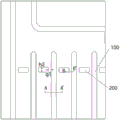
目前,在半导体器件技术中,沟槽结构的侧氧(Oxide-Bypassed OB)技术被广泛应用,被应用在中低压MOSFET以及沟槽肖特基(TMBS)等器件中,对于快回复二极管(Fastrecovery diode,FRD)、绝缘栅双极型晶体管(Insulated Gate Bipolar Transistor,IGBT)器件也有被采用,其中,如屏蔽栅MOSFET器件等是典型的量产产品。在这类半导体器件的终端结构中,如图1中终端处(图1所示A处)、栅PAD处(图1所示B处)位置,主要由沟槽及附在沟槽内表面的规定厚度的场氧化层以及深入其中多晶场板构成沟槽场板,沟槽场板在器件边缘排布形成器件终端结构。沟槽场板中场氧化层形成的工艺有从沟槽内壁通过热氧化方式形成,也有通过化学气相沉积(Chemical VaporDeposition,CVD)形成,或是通过热氧化和CVD组合方式形成。主流终端沟槽场板结构排布如图2A和图2B所示,该结构若要达到最高的耐电压值,在终端处有源区的沟槽与边缘沟槽弯曲90°后的沟槽围成的外延层区6宽度b与有源区的沟槽分隔的外延层区6宽度a之间存在一个最佳比例,偏离这个比例,耐电压值就会降低。但实际工艺中因光刻CD、沟槽中场氧化层形成工艺、以及沟槽刻蚀宽度的均匀性等因素都会影响这个优化比例,使器件电压很难达到最高耐压。At present, in the semiconductor device technology, the Oxide-Bypassed OB technology of the trench structure is widely used, and is used in low-voltage MOSFETs and Trench Schottky (TMBS) and other devices. For Fastrecovery diodes (Fastrecovery diode, FRD) and insulated gate bipolar transistor (Insulated Gate Bipolar Transistor, IGBT) devices are also used, among which shielded gate MOSFET devices are typical mass-produced products. In the terminal structure of this type of semiconductor device, as shown in Figure 1, the position of the terminal (A in Figure 1) and the gate PAD (B in Figure 1) is mainly composed of the trench and the groove attached to the inner surface of the trench. A field oxide layer with a specified thickness and a polycrystalline field plate penetrating into it form a trench field plate, and the trench field plates are arranged on the edge of the device to form a device terminal structure. The process for forming the field oxide layer of the trench field plate includes thermal oxidation from the inner wall of the trench, chemical vapor deposition (Chemical Vapor Deposition, CVD), or a combination of thermal oxidation and CVD. The layout of the mainstream terminal groove field plate structure is shown in Figure 2A and Figure 2B. To achieve the highest withstand voltage value of this structure, the trench in the active region at the terminal and the edge groove are bent by 90°. There is an optimal ratio between the width b of the formed
发明内容Contents of the invention
为了克服上述技术背景中所提及的技术问题,本申请实施例提供一种半导体器件终端结构,所述半导体器件终端结构包括:In order to overcome the technical problems mentioned in the above technical background, an embodiment of the present application provides a semiconductor device terminal structure, the semiconductor device terminal structure includes:
形成于外延层上的至少两个平行的屏蔽栅沟槽,所述屏蔽栅沟槽内侧覆盖有第一绝缘氧化物层并设置有第一多晶硅;At least two parallel shielding gate trenches formed on the epitaxial layer, the inside of the shielding gate trenches are covered with a first insulating oxide layer and provided with first polysilicon;
位于相邻两个所述屏蔽栅沟槽之间、靠近所述屏蔽栅沟槽端部位置的隔离沟槽,所述隔离沟槽中设置有第二绝缘氧化物层,所述隔离沟槽中的第一绝缘氧化物层与所述屏蔽栅沟槽中的第二绝缘氧化物层连通。An isolation trench located between two adjacent shielding gate trenches and close to the end of the shielding gate trench, a second insulating oxide layer is arranged in the isolation trench, and in the isolation trench The first insulating oxide layer communicates with the second insulating oxide layer in the shielding gate trench.
在一种可能的实现方式中,所述隔离沟槽被所述第二绝缘氧化物层完全填充。In a possible implementation manner, the isolation trench is completely filled by the second insulating oxide layer.
在一种可能的实现方式中,所述屏蔽栅沟槽内侧覆盖的第一绝缘氧化物层的单层厚度为第一材料厚度,所述隔离沟槽在垂直于至少所述屏蔽栅沟槽的排列方向上的宽度大于所述第一材料厚度且小于所述第一材料厚度的2倍。In a possible implementation manner, the thickness of a single layer of the first insulating oxide layer covering the inside of the shielding gate trench is the first material thickness, and the isolation trench is perpendicular to at least the shielding gate trench. The width in the arrangement direction is greater than the thickness of the first material and less than twice the thickness of the first material.
在一种可能的实现方式中,所述隔离沟槽中还包括被所述第二绝缘氧化物层包裹的第二多晶硅。In a possible implementation manner, the isolation trench further includes second polysilicon wrapped by the second insulating oxide layer.
在一种可能的实现方式中,所述屏蔽栅沟槽内侧覆盖的第一绝缘氧化物层的单层厚度为第一材料厚度,所述第二多晶硅和所述第一多晶硅之间的最短距离大于所述第一材料厚度且小于所述第一材料厚度的2倍。In a possible implementation manner, the thickness of a single layer of the first insulating oxide layer covering the inner side of the shielding gate trench is the first material thickness, and the thickness between the second polysilicon and the first polysilicon is The shortest distance between them is greater than the thickness of the first material and less than twice the thickness of the first material.
在一种可能的实现方式中,所述半导体器件终端结构还包括:In a possible implementation manner, the terminal structure of the semiconductor device further includes:
形成于所述外延层上的至少一段边缘沟槽,所述边缘沟槽平行于至少两个所述屏蔽栅沟槽的排列方向,所述边缘沟槽内侧覆盖有第一绝缘氧化物层并设置有第三多晶硅。At least one section of edge trenches formed on the epitaxial layer, the edge trenches are parallel to the arrangement direction of at least two shielding gate trenches, the inside of the edge trenches is covered with a first insulating oxide layer and set There is a third polysilicon.
本申请还提供一种半导体器件终端结构的制造方法,所述方法包括:The present application also provides a method for manufacturing a terminal structure of a semiconductor device, the method comprising:
在外延层上通过刻蚀形成至少两个平行的屏蔽栅沟槽及位于相邻两个所述屏蔽栅沟槽之间的隔离沟槽;Forming at least two parallel shielding gate trenches and an isolation trench between two adjacent shielding gate trenches by etching on the epitaxial layer;
在所述屏蔽栅沟槽内侧形成第一绝缘氧化物层,并在所述隔离沟槽中形成第二绝缘氧化物层,使所述第一绝缘氧化物层和所述第二绝缘氧化物层连通;A first insulating oxide layer is formed inside the shielding gate trench, and a second insulating oxide layer is formed in the isolation trench, so that the first insulating oxide layer and the second insulating oxide layer connected;
在所述屏蔽栅沟槽中填充第一多晶硅。The shielding gate trench is filled with first polysilicon.
在一种可能的实现方式中,所述在外延层上通过刻蚀形成至少两个平行的屏蔽栅沟槽及位于相邻两个所述屏蔽栅沟槽之间的隔离沟槽的步骤,包括:In a possible implementation manner, the step of forming at least two parallel shielding gate trenches and an isolation trench between two adjacent shielding gate trenches by etching on the epitaxial layer includes :
在所述外延层上形成通过刻蚀形成至少两个平行屏蔽栅沟槽,并通过刻蚀形成位于相邻两个所述屏蔽栅沟槽之间且连通所述两个所述屏蔽栅沟槽的隔离沟槽;在与至少两个所述屏蔽栅沟槽排列方向平行的方向上,所述屏蔽栅沟槽的宽度为第一宽度;在与至少两个所述屏蔽栅沟槽排列方向垂直的方向上,所述隔离沟槽的宽度为第二宽度;所述第一宽度大于所述第二宽度的2倍;Form at least two parallel shielding gate trenches by etching on the epitaxial layer, and form a shielding gate trench between adjacent two shielding gate trenches and communicate with the two shielding gate trenches by etching. isolation trenches; in a direction parallel to the arrangement direction of at least two of the shielding gate trenches, the width of the shielding gate trenches is a first width; in a direction perpendicular to the arrangement direction of at least two of the shielding gate trenches In the direction of , the width of the isolation trench is the second width; the first width is greater than twice the second width;
所述在所述屏蔽栅沟槽内侧形成第一绝缘氧化物层及所述隔离沟槽中形成第二绝缘氧化物层的步骤,包括:The step of forming a first insulating oxide layer inside the shielding gate trench and forming a second insulating oxide layer in the isolation trench includes:
通过化学气相沉积法在所述屏蔽栅沟槽第一材料厚度的第一绝缘氧化物层,并在所述隔离沟槽内第二绝缘氧化物层将所述隔离沟槽填充满,所述第二宽度大于所述第一材料厚度且小于所述第一材料厚度的2倍。A first insulating oxide layer with a first material thickness in the shielding gate trench by chemical vapor deposition, and a second insulating oxide layer in the isolation trench fills the isolation trench, and the first insulating oxide layer fills the isolation trench. The second width is greater than the thickness of the first material and less than twice the thickness of the first material.
在一种可能的实现方式中,所述在外延层上通过刻蚀形成至少两个平行的屏蔽栅沟槽及位于相邻两个所述屏蔽栅沟槽之间的隔离沟槽的步骤,包括:In a possible implementation manner, the step of forming at least two parallel shielding gate trenches and an isolation trench between two adjacent shielding gate trenches by etching on the epitaxial layer includes :
在所述外延层上形成通过刻蚀形成至少两个平行屏蔽栅沟槽,并通过刻蚀形成位于相邻两个所述屏蔽栅沟槽之间且与所述两个所述屏蔽栅沟槽存在间隔的隔离沟槽;在与至少两个所述屏蔽栅沟槽的排列方向垂直的方向上,所述隔离沟槽的宽度为第三宽度;在与至少两个所述屏蔽栅沟槽的排列方向平行的方向上,所述隔离沟槽与所述屏蔽栅沟槽之间的间隔为第四宽度;所述第三宽度大于所述第四宽度;Form at least two parallel shielding gate trenches by etching on the epitaxial layer, and form by etching between adjacent two shielding gate trenches and between the two shielding gate trenches There are spaced isolation trenches; in a direction perpendicular to the arrangement direction of at least two shielding gate trenches, the width of the isolation trenches is a third width; In a direction parallel to the arrangement direction, the interval between the isolation trench and the shielding gate trench is a fourth width; the third width is greater than the fourth width;
所述在所述屏蔽栅沟槽内侧形成第一绝缘氧化物层及所述隔离沟槽中形成第二绝缘氧化物层的步骤,包括:The step of forming a first insulating oxide layer inside the shielding gate trench and forming a second insulating oxide layer in the isolation trench includes:
通过硅热氧化处理在所述屏蔽栅沟槽内侧进行形成第一绝缘氧化物层,并在所述隔离沟槽内侧进行形成第二绝缘氧化物层,所述硅热氧化处理所消耗掉的硅的厚度为第一材料厚度,所述第一材料厚度的两倍大于所述第四宽度;A first insulating oxide layer is formed inside the shielding gate trench by silicon thermal oxidation treatment, and a second insulating oxide layer is formed inside the isolation trench. The silicon thermal oxidation treatment consumes silicon The thickness is the first material thickness, twice the first material thickness is greater than the fourth width;
所述在所述屏蔽栅沟槽中填充第一多晶硅的步骤,包括:The step of filling the first polysilicon in the shielding gate trench includes:
在所述屏蔽栅沟槽中填充第一多晶硅,并在所述隔离沟槽中填充第二多晶硅。The shielding gate trench is filled with first polysilicon, and the isolation trench is filled with second polysilicon.
本申请还提供一种半导体器件,所述半导体器件包括本申请提供的所述半导体器件终端结构。The present application also provides a semiconductor device, which includes the terminal structure of the semiconductor device provided in the present application.
本申请实施例提供的半导体器件终端结构、制造方法及半导体器件,通过在终端处相邻两个屏蔽栅沟槽之间设置填充有绝缘氧化材料的隔离沟槽,隔离沟槽将屏蔽栅沟槽界定出的外延层区隔离开,可以使靠近隔离沟槽的有源区内的外延层区和有源区深处的外延层区具有基本相同的电场分布,从而有效提高终端结构的最高耐压,并且不受实际工艺中光刻、沟槽中场氧化层形成工艺、以及沟槽刻蚀宽度的均匀性等因素产生影响,降低了芯片制造的工艺难度,可以提升芯片制造的效率。In the semiconductor device terminal structure, manufacturing method and semiconductor device provided by the embodiments of the present application, an isolation trench filled with an insulating oxide material is provided between two adjacent shielding gate trenches at the terminal, and the isolation trench connects the shielding gate trenches to The defined epitaxial layer region is isolated, so that the epitaxial layer region in the active region close to the isolation trench and the epitaxial layer region deep in the active region have basically the same electric field distribution, thereby effectively improving the highest withstand voltage of the terminal structure , and is not affected by factors such as photolithography, trench field oxide layer formation process, and trench etching width uniformity in the actual process, which reduces the process difficulty of chip manufacturing and can improve the efficiency of chip manufacturing.
附图说明Description of drawings
为了更清楚地说明本申请实施例的技术方案,下面将对实施例中所需要使用的附图作简单地介绍,应当理解,以下附图仅示出了本申请的某些实施例,因此不应被看作是对范围的限定,对于本领域普通技术人员来讲,在不付出创造性劳动的前提下,还可以根据这些附图获得其他相关的附图。In order to more clearly illustrate the technical solutions of the embodiments of the present application, the following will briefly introduce the accompanying drawings used in the embodiments. It should be understood that the following drawings only show some embodiments of the present application, so It should be regarded as a limitation on the scope, and those skilled in the art can also obtain other related drawings based on these drawings without creative work.
图1为沟槽场板的示意图;1 is a schematic diagram of a trench field plate;
图2A和图2B为现有技术中终端沟槽场板结构排布示意图;FIG. 2A and FIG. 2B are schematic diagrams of the arrangement of terminal trench field plate structures in the prior art;
图3A和图3B为本申请实施例提供的半导体器件终端结构的示意图之一;3A and 3B are one of the schematic diagrams of the terminal structure of the semiconductor device provided by the embodiment of the present application;
图4A和图4B为本申请实施例提供的半导体器件终端结构的示意图之二;FIG. 4A and FIG. 4B are the second schematic diagrams of the terminal structure of the semiconductor device provided by the embodiment of the present application;
图5为本申请实施例提供的半导体器件终端结构的制造方法的流程示意图;FIG. 5 is a schematic flowchart of a method for manufacturing a terminal structure of a semiconductor device provided in an embodiment of the present application;
图6A、图6B和图6C为本申请实施例提供的半导体器件终端结构的制作过程示意图之一;FIG. 6A, FIG. 6B and FIG. 6C are one of the schematic diagrams of the manufacturing process of the semiconductor device terminal structure provided by the embodiment of the present application;
图7A、图7B和图7C为本申请实施例提供的半导体器件终端结构的制作过程示意图之二;FIG. 7A, FIG. 7B and FIG. 7C are the second schematic diagrams of the manufacturing process of the semiconductor device terminal structure provided by the embodiment of the present application;
图8A、图8B和图8C为本申请实施例提供的半导体器件终端结构的制作过程示意图之三;FIG. 8A, FIG. 8B and FIG. 8C are the third schematic diagrams of the manufacturing process of the semiconductor device terminal structure provided by the embodiment of the present application;
图9A、图9B和图9C为本申请实施例提供的半导体器件终端结构的制作过程示意图之四。FIG. 9A , FIG. 9B and FIG. 9C are the fourth schematic diagrams of the manufacturing process of the semiconductor device terminal structure provided by the embodiment of the present application.
具体实施方式Detailed ways
为使本申请实施例的目的、技术方案和优点更加清楚,下面将结合本申请实施例中的附图,对本申请实施例中的技术方案进行清楚、完整地描述,显然,所描述的实施例是本申请一部分实施例,而不是全部的实施例。通常在此处附图中描述和示出的本申请实施例的组件可以以各种不同的配置来布置和设计。In order to make the purposes, technical solutions and advantages of the embodiments of the present application clearer, the technical solutions in the embodiments of the present application will be clearly and completely described below in conjunction with the drawings in the embodiments of the present application. Obviously, the described embodiments It is a part of the embodiments of this application, not all of them. The components of the embodiments of the application generally described and illustrated in the figures herein may be arranged and designed in a variety of different configurations.
因此,以下对在附图中提供的本申请的实施例的详细描述并非旨在限制要求保护的本申请的范围,而是仅仅表示本申请的选定实施例。基于本申请中的实施例,本领域普通技术人员在没有作出创造性劳动前提下所获得的所有其他实施例,都属于本申请保护的范围。Accordingly, the following detailed description of the embodiments of the application provided in the accompanying drawings is not intended to limit the scope of the claimed application, but merely represents selected embodiments of the application. Based on the embodiments in this application, all other embodiments obtained by persons of ordinary skill in the art without creative efforts fall within the protection scope of this application.
应注意到:相似的标号和字母在下面的附图中表示类似项,因此,一旦某一项在一个附图中被定义,则在随后的附图中不需要对其进行进一步定义和解释。It should be noted that like numerals and letters denote similar items in the following figures, therefore, once an item is defined in one figure, it does not require further definition and explanation in subsequent figures.
在本申请的描述中,需要说明的是,术语“上”、“下”等指示的方位或位置关系为基于附图所示的方位或位置关系,或者是该申请产品使用时惯常摆放的方位或位置关系,仅是为了便于描述本申请和简化描述,而不是指示或暗示所指的装置或元件必须具有特定的方位、以特定的方位构造和操作,因此不能理解为对本申请的限制。此外,术语“第一”、“第二”等仅用于区分描述,而不能理解为指示或暗示相对重要性。In the description of this application, it should be noted that the orientation or positional relationship indicated by the terms "upper", "lower" and so on is based on the orientation or positional relationship shown in the attached drawings, or the usual placement of the application product when it is used. Orientation or positional relationship is only for the convenience of describing the present application and simplifying the description, and does not indicate or imply that the referred device or element must have a specific orientation, be constructed and operated in a specific orientation, and thus should not be construed as limiting the present application. In addition, the terms "first", "second", etc. are only used for distinguishing descriptions, and should not be construed as indicating or implying relative importance.
需要说明的是,在不冲突的情况下,本申请的实施例中的不同特征之间可以相互结合。It should be noted that, in the case of no conflict, different features in the embodiments of the present application may be combined with each other.
请参照图3A和图3B,图3A和图3B为本实施例提供的半导体器件终端结构的示意图,所述半导体器件终端结构包括至少两个屏蔽栅沟槽及隔离沟槽。Please refer to FIG. 3A and FIG. 3B . FIG. 3A and FIG. 3B are schematic diagrams of a terminal structure of a semiconductor device provided by this embodiment. The terminal structure of a semiconductor device includes at least two shielding gate trenches and isolation trenches.
所述至少两个屏蔽栅沟槽形成于外延层上且相互平行,所述至少两个屏蔽栅沟槽可以位于芯片的有源区内,由所述至少两个屏蔽栅沟槽分割形成JFET区。The at least two shielding gate trenches are formed on the epitaxial layer and are parallel to each other, the at least two shielding gate trenches may be located in the active area of the chip, and the JFET region is formed by dividing the at least two shielding gate trenches .
所述屏蔽栅沟槽内侧覆盖有第一绝缘氧化物层1并设置有第一多晶硅2。例如,在屏蔽栅沟槽内设置有由第一绝缘氧化物层1包裹的第一多晶硅2,第一多晶硅2不与屏蔽栅沟槽的内壁接触。可选地,第一绝缘氧化物层1可以为场氧层。The inside of the shielding gate trench is covered with a first insulating
所述隔离沟槽位于相邻两个所述屏蔽栅沟槽之间且靠近所述屏蔽栅沟槽端部位置。所述隔离沟槽中设置有第二绝缘氧化物层3,所述隔离沟槽中的第二绝缘氧化物层3与所述屏蔽栅沟槽中的第一绝缘氧化物层1连通。其中,所述第二绝缘氧化物层3和所述第一绝缘氧化物层1可以是相同的材料,或者由相同的工艺形成。The isolation trench is located between two adjacent shielding gate trenches and close to the ends of the shielding gate trenches. A second insulating
在一种可能的实现方式中,请再次参照图3A和图3B,所述隔离沟槽被所述第二绝缘氧化物层3完全填充。In a possible implementation manner, please refer to FIG. 3A and FIG. 3B again, the isolation trench is completely filled with the second insulating
进一步地,在这种实现方式中,所述屏蔽栅沟槽内侧覆盖的第一绝缘氧化物层1的单层厚度为第一材料厚度,所述隔离沟槽在垂直于至少所述屏蔽栅沟槽的排列方向上的宽度大于所述第一材料厚度且小于所述第一材料厚度的2倍。也就是说,所述隔离沟槽在沿所述屏蔽栅沟槽的延伸方向上的宽度大于所述第一材料厚度且小于所述第一材料厚度的2倍。Further, in this implementation manner, the thickness of a single layer of the first insulating
在另一种可能的实现方式中,请参照图4A和图4B,所述隔离沟槽中还可以设置有被所述第二绝缘氧化物层3包裹的第二多晶硅4。所述第二多晶硅4不与所述隔离沟槽内壁接触,且不与所述第一多晶硅2接触,也不与任何电极接触。其中,所述第二多晶硅4和所述第一多晶硅2可以为相同的材料,或者有相同的工艺形成。In another possible implementation manner, please refer to FIG. 4A and FIG. 4B , a
进一步地,在这种实现方式中,所述屏蔽栅沟槽内侧覆盖的第一绝缘氧化物层1的单层厚度为第一材料厚度,所述第二多晶硅4和所述第一多晶硅2之间的最短距离大于所述第一材料厚度且小于所述第一材料厚度的2倍。Further, in this implementation manner, the thickness of a single layer of the first insulating
可选地,请再次参照图3A、图3B、图4A和图4B,所述半导体器件终端结构还可以包括边缘沟槽,所述边缘沟槽平行于至少两个所述屏蔽栅沟槽的排列方向,所述边缘沟槽内侧覆盖有第一绝缘氧化物层1并设置有第三多晶硅5。所述第三多晶硅5和所述第一多晶硅2可以为相同的材料,或者有相同的工艺形成。Optionally, please refer to FIG. 3A, FIG. 3B, FIG. 4A and FIG. 4B again, the terminal structure of the semiconductor device may further include edge trenches, and the edge trenches are parallel to the arrangement of at least two shielding gate trenches. direction, the inside of the edge trench is covered with a first insulating
请参照图5,图5为本实施例提供的一种半导体器件终端结构的制造方法,下面对该方法的各个步骤进行详细阐述。Please refer to FIG. 5 . FIG. 5 is a method for manufacturing a terminal structure of a semiconductor device provided in this embodiment. Each step of the method will be described in detail below.
步骤S110,在外延层上通过刻蚀形成至少两个平行的屏蔽栅沟槽100及位于相邻两个所述屏蔽栅沟槽100之间的隔离沟槽200。Step S110 , forming at least two parallel
在本实施例中,可以通过使用掩膜的光刻工艺在预先形成的外延层上刻蚀形成所述屏蔽栅沟槽100及所述隔离沟槽200。其中,所述至少两个屏蔽栅沟槽100相互平行,所述隔离沟槽200位于相邻两个所述屏蔽栅沟槽100之间且靠近所述屏蔽栅沟槽100端部位置。In this embodiment, the shielding
步骤S120,在所述屏蔽栅沟槽100内侧形成第一绝缘氧化物层1,并在所述隔离沟槽200中形成第二绝缘氧化物层3,使所述第一绝缘氧化物层1和所述第二绝缘氧化物层3连通。Step S120, forming a first insulating
在本实施例中,所述第二绝缘氧化物层3和所述第一绝缘氧化物层1可以是相同的材料,或者由相同的工艺形成。例如,通过化学气相沉积工艺或者硅热氧化工艺同时在所述屏蔽栅沟槽100和所述隔离沟槽200内侧分别形成所述第一绝缘氧化物层1和所述第二绝缘氧化物层3。In this embodiment, the second insulating
步骤S130,在所述屏蔽栅沟槽100中填充第一多晶硅2。Step S130 , filling the
在本实施例中,在所述屏蔽栅沟槽100中形成第一绝缘氧化物层1后,所述屏蔽栅沟槽100中还可以存在一定的空间,然后可以在该空间内填充第一多晶硅2,使所述第一多晶硅2被所述第一绝缘氧化物层1包裹。In this embodiment, after the first insulating
在一种可能的实现方式中,请参照图6A和图6B,在步骤S110中,可以在所述外延层上形成通过刻蚀形成至少两个平行屏蔽栅沟槽100,并通过刻蚀形成位于相邻两个所述屏蔽栅沟槽100之间且连通所述两个所述屏蔽栅沟槽100的隔离沟槽200。In a possible implementation, please refer to FIG. 6A and FIG. 6B. In step S110, at least two parallel
请参照图6C,图6C为图6A和图6B在AA’和BB’方向上的剖面图,在与至少两个所述屏蔽栅沟槽100排列方向平行的方向上,所述屏蔽栅沟槽100的宽度为第一宽度w1;在与至少两个所述屏蔽栅沟槽100排列方向垂直的方向上,所述隔离沟槽200的宽度为第二宽度h1。所述第一宽度w1大于所述第二宽度h1的2倍。Please refer to FIG. 6C. FIG. 6C is a cross-sectional view of FIG. 6A and FIG. 6B in the direction of AA' and BB'. The width of the
请参照图7A和图7B,在步骤S120中,可以通过化学气相沉积法在所述屏蔽栅沟槽100第一材料厚度w2的第一绝缘氧化物层1,并在所述隔离沟槽200内第二绝缘氧化物层3将所述隔离沟槽200填充满。可选地,所述第一绝缘氧化物层1及第二绝缘氧化物层3可以完全化学气相沉积法形成;或者,所述第一绝缘氧化物层1及所述第二绝缘氧化物层3也可以部分由化学气相沉积法形成,例如,首先在所述屏蔽栅沟槽100和所述隔离沟槽200的内壁通过热氧化工艺形成一层比较薄的氧化层,再通过形成所述第一绝缘氧化物层1及第二绝缘氧化物层3。Please refer to FIG. 7A and FIG. 7B. In step S120, the first insulating
请参照图7C,图7C为图7A和图7B在AA’和BB’方向上的剖面图,所述第二宽度h1大于所述第一材料厚度w2且小于所述第一材料厚度w2的2倍。例如,隔离沟槽200的第二宽度h1可以为第一绝缘氧化物层1的第一材料厚度w2的1.5倍。Please refer to FIG. 7C, FIG. 7C is a cross-sectional view of FIG. 7A and FIG. 7B in the direction of AA' and BB', the second width h1 is greater than the first material thickness w2 and less than 2% of the first material thickness w2 times. For example, the second width h1 of the
在另一种可能的实现方式中,请参照图8A和图8B,在步骤S110中,可以在所述外延层上形成通过刻蚀形成至少两个平行屏蔽栅沟槽100,并通过刻蚀形成位于相邻两个所述屏蔽栅沟槽100之间且与所述两个所述屏蔽栅沟槽100存在间隔的隔离沟槽200。In another possible implementation, please refer to FIG. 8A and FIG. 8B , in step S110, at least two parallel
请参照图8C,图8C为图8A和图8B在AA’和BB’方向上的剖面图,在与至少两个所述屏蔽栅沟槽100的排列方向垂直的方向上,所述隔离沟槽200的宽度为第三宽度h2;在与至少两个所述屏蔽栅沟槽100的排列方向平行的方向上,所述隔离沟槽200与所述屏蔽栅沟槽100之间的间隔为第四宽度g1;所述第三宽度h2大于所述第四宽度g1,Please refer to FIG. 8C. FIG. 8C is a cross-sectional view of FIG. 8A and FIG. 8B in the direction of AA' and BB'. The width of 200 is the third width h2; in the direction parallel to the arrangement direction of at least two shielding
请参照图9A和图9B,在步骤S120中,可以通过硅热氧化处理在所述屏蔽栅沟槽100内侧进行形成第一绝缘氧化物层1,并在所述隔离沟槽200内侧进行形成第二绝缘氧化物层3。请参照图8C,图8C为图8A和图8B在AA’和BB’方向上的剖面图,所述硅热氧化处理所消耗掉的硅的厚度为第一材料厚度w2,所述第一材料厚度w2的两倍大于所述第四宽度g1。例如,所述第一材料厚度w2的为所述第四宽度g1的1.5倍。换句话说,隔离沟槽200壁的硅在第四宽度对应的位置上,从两侧被所述硅热氧化处理所完全消耗掉,形成第四宽度g1绝缘氧化物。9A and 9B, in step S120, a first insulating
在步骤S130中,可以在所述屏蔽栅沟槽100中填充第一多晶硅2,并在所述隔离沟槽200中填充第二多晶硅4。请再次参照图4,在填充第一多晶硅2和第二多晶硅4后,第一多晶硅2被第一绝缘氧化绝缘材料层包裹,第二多晶硅4被第二绝缘氧化物层3包裹。In step S130 , the
可选地,在本实施例中,在步骤S110中形成所述屏蔽栅沟槽100和所述隔离沟槽200时,还可以同时形成所述边缘沟槽,所述边缘沟槽平行于至少两个所述屏蔽栅沟槽100的排列方向。在步骤S120中,在所述屏蔽栅沟槽100中形成所述第一绝缘氧化物层1时,还可以在所述边缘沟槽中同时形成第一绝缘氧化物层1。在步骤S130中,在形成所述第一多晶硅2时,还可以在所述边缘沟槽中形成所述第三多晶硅5。Optionally, in this embodiment, when forming the shielding
本实施例还提供一种半导体器件,该半导体器件可以包括本实施例提供的半导体器件终端结构。This embodiment also provides a semiconductor device, which may include the terminal structure of the semiconductor device provided by this embodiment.
本申请实施例提供的半导体器件终端结构、制造方法及半导体器件,通过在终端处相邻两个屏蔽栅沟槽之间设置填充有绝缘氧化材料的隔离沟槽,隔离沟槽将屏蔽栅沟槽界定出的外延层区隔离开,可以使靠近隔离沟槽的有源区内的外延层区和有源区深处的外延层区具有基本相同的电场分布,从而有效提高终端结构的最高耐压,并且不受实际工艺中光刻、沟槽中场氧化层形成工艺、以及沟槽刻蚀宽度的均匀性等因素产生影响,降低了芯片制造的工艺难度,可以提升芯片制造的效率。In the semiconductor device terminal structure, manufacturing method and semiconductor device provided by the embodiments of the present application, an isolation trench filled with an insulating oxide material is provided between two adjacent shielding gate trenches at the terminal, and the isolation trench connects the shielding gate trenches to The defined epitaxial layer region is isolated, so that the epitaxial layer region in the active region close to the isolation trench and the epitaxial layer region deep in the active region have basically the same electric field distribution, thereby effectively improving the highest withstand voltage of the terminal structure , and is not affected by factors such as photolithography, trench field oxide layer formation process, and trench etching width uniformity in the actual process, which reduces the process difficulty of chip manufacturing and can improve the efficiency of chip manufacturing.
以上所述实施例的各技术特征可以进行任意的组合,为使描述简洁,未对上述实施例中的各个技术特征所有可能的组合都进行描述,然而,只要这些技术特征的组合不存在矛盾,都应当认为是本说明书记载的范围。The technical features of the above-mentioned embodiments can be combined arbitrarily. To make the description concise, all possible combinations of the technical features in the above-mentioned embodiments are not described. However, as long as there is no contradiction in the combination of these technical features, should be considered as within the scope of this specification.
以上所述实施例仅表达了本发明的几种实施方式,其描述较为具体和详细,但并不能因此而理解为对发明专利范围的限制。应当指出的是,对于本领域的普通技术人员来说,在不脱离本发明构思的前提下,还可以做出若干变形和改进,这些都属于本发明的保护范围。因此,本发明专利的保护范围应以所附权利要求为准。The above-mentioned embodiments only express several implementation modes of the present invention, and the descriptions thereof are relatively specific and detailed, but should not be construed as limiting the patent scope of the invention. It should be pointed out that those skilled in the art can make several modifications and improvements without departing from the concept of the present invention, and these all belong to the protection scope of the present invention. Therefore, the protection scope of the patent for the present invention should be based on the appended claims.
Claims (6)
Priority Applications (1)
| Application Number | Priority Date | Filing Date | Title |
|---|---|---|---|
| CN202110577656.XA CN113206146B (en) | 2021-05-26 | 2021-05-26 | Semiconductor device terminal structure, manufacturing method and semiconductor device |
Applications Claiming Priority (1)
| Application Number | Priority Date | Filing Date | Title |
|---|---|---|---|
| CN202110577656.XA CN113206146B (en) | 2021-05-26 | 2021-05-26 | Semiconductor device terminal structure, manufacturing method and semiconductor device |
Publications (2)
| Publication Number | Publication Date |
|---|---|
| CN113206146A CN113206146A (en) | 2021-08-03 |
| CN113206146B true CN113206146B (en) | 2023-03-24 |
Family
ID=77023363
Family Applications (1)
| Application Number | Title | Priority Date | Filing Date |
|---|---|---|---|
| CN202110577656.XA Active CN113206146B (en) | 2021-05-26 | 2021-05-26 | Semiconductor device terminal structure, manufacturing method and semiconductor device |
Country Status (1)
| Country | Link |
|---|---|
| CN (1) | CN113206146B (en) |
Citations (1)
| Publication number | Priority date | Publication date | Assignee | Title |
|---|---|---|---|---|
| CN109216175A (en) * | 2017-07-03 | 2019-01-15 | 无锡华润上华科技有限公司 | The gate structure and its manufacturing method of semiconductor devices |
Family Cites Families (11)
| Publication number | Priority date | Publication date | Assignee | Title |
|---|---|---|---|---|
| JP4276510B2 (en) * | 2003-10-02 | 2009-06-10 | 株式会社東芝 | Semiconductor memory device and manufacturing method thereof |
| JP2006093545A (en) * | 2004-09-27 | 2006-04-06 | Nissan Motor Co Ltd | Semiconductor device |
| US7453119B2 (en) * | 2005-02-11 | 2008-11-18 | Alphs & Omega Semiconductor, Ltd. | Shielded gate trench (SGT) MOSFET cells implemented with a schottky source contact |
| US20110254071A1 (en) * | 2009-11-20 | 2011-10-20 | Force Mos Technology Co. Ltd. | Shielded trench mosfet with multiple trenched floating gates as termination |
| US8319290B2 (en) * | 2010-06-18 | 2012-11-27 | Fairchild Semiconductor Corporation | Trench MOS barrier schottky rectifier with a planar surface using CMP techniques |
| JP6423110B2 (en) * | 2015-04-30 | 2018-11-14 | 蘇州東微半導体有限公司 | Semiconductor superjunction power device and manufacturing method thereof |
| US10714574B2 (en) * | 2018-05-08 | 2020-07-14 | Ipower Semiconductor | Shielded trench devices |
| CN110957357B (en) * | 2018-09-27 | 2023-06-02 | 力士科技股份有限公司 | Manufacturing method of shielded gate type metal oxide half field effect transistor |
| CN110620146B (en) * | 2019-09-24 | 2023-05-12 | 吉林华微电子股份有限公司 | Field plate structure and semiconductor device |
| CN112038408B (en) * | 2020-09-04 | 2021-11-23 | 西安电子科技大学 | Vertical aluminum nitride metal oxide semiconductor field effect transistor based on silicon carbide substrate and preparation method |
| CN112509980B (en) * | 2020-11-30 | 2022-06-03 | 绍兴中芯集成电路制造股份有限公司 | Semiconductor device having a shielded gate trench structure and method of manufacturing the same |
-
2021
- 2021-05-26 CN CN202110577656.XA patent/CN113206146B/en active Active
Patent Citations (1)
| Publication number | Priority date | Publication date | Assignee | Title |
|---|---|---|---|---|
| CN109216175A (en) * | 2017-07-03 | 2019-01-15 | 无锡华润上华科技有限公司 | The gate structure and its manufacturing method of semiconductor devices |
Also Published As
| Publication number | Publication date |
|---|---|
| CN113206146A (en) | 2021-08-03 |
Similar Documents
| Publication | Publication Date | Title |
|---|---|---|
| CN112447847B (en) | Semiconductor device and manufacturing method thereof | |
| JP3531613B2 (en) | Trench gate type semiconductor device and manufacturing method thereof | |
| JP5640969B2 (en) | Semiconductor element | |
| US9614073B2 (en) | Semiconductor device, and manufacturing method for same | |
| CN110010687A (en) | Semiconductor device with a plurality of transistors | |
| JP2012019188A (en) | Semiconductor device and method of manufacturing semiconductor device | |
| JP2007242852A (en) | Insulated gate semiconductor device and manufacturing method thereof | |
| JP2012204529A (en) | Semiconductor device and method of manufacturing the same | |
| US10332967B2 (en) | Semiconductor device and method for manufacturing the same | |
| WO2013168796A1 (en) | Semiconductor device and method for producing semiconductor device | |
| JP7647042B2 (en) | Semiconductor device and method for manufacturing the same | |
| US8017494B2 (en) | Termination trench structure for mosgated device and process for its manufacture | |
| WO2020218378A1 (en) | Semiconductor device, and manufacturing method therefor | |
| CN111564493A (en) | Trench power transistor and method of making the same | |
| US11264462B2 (en) | Silicon carbide semiconductor device and method of manufacturing silicon carbide semiconductor device | |
| JP3960091B2 (en) | Semiconductor device and manufacturing method thereof | |
| CN113206146B (en) | Semiconductor device terminal structure, manufacturing method and semiconductor device | |
| US11594629B2 (en) | Semiconductor device | |
| WO2021157529A1 (en) | Semiconductor device | |
| CN118919565A (en) | VDMOS device and preparation method thereof | |
| JP7556798B2 (en) | Semiconductor device and semiconductor package | |
| TW201935693A (en) | Power semiconductor device | |
| CN111710722A (en) | Lateral double diffused transistor and method of making the same | |
| US12249633B2 (en) | Field-effect transistor and method for manufacturing field-effect transistor | |
| US20240096972A1 (en) | Semiconductor device |
Legal Events
| Date | Code | Title | Description |
|---|---|---|---|
| PB01 | Publication | ||
| PB01 | Publication | ||
| SE01 | Entry into force of request for substantive examination | ||
| SE01 | Entry into force of request for substantive examination | ||
| GR01 | Patent grant | ||
| GR01 | Patent grant |