CN113161760B - An all-dielectric multiband terahertz metamaterial absorber with randomly distributed cells - Google Patents
An all-dielectric multiband terahertz metamaterial absorber with randomly distributed cells Download PDFInfo
- Publication number
- CN113161760B CN113161760B CN202110234078.XA CN202110234078A CN113161760B CN 113161760 B CN113161760 B CN 113161760B CN 202110234078 A CN202110234078 A CN 202110234078A CN 113161760 B CN113161760 B CN 113161760B
- Authority
- CN
- China
- Prior art keywords
- etching
- units
- grid
- grids
- randomly distributed
- Prior art date
- Legal status (The legal status is an assumption and is not a legal conclusion. Google has not performed a legal analysis and makes no representation as to the accuracy of the status listed.)
- Active
Links
- 239000006096 absorbing agent Substances 0.000 title claims abstract description 23
- 238000005530 etching Methods 0.000 claims abstract description 69
- 239000000758 substrate Substances 0.000 claims abstract description 18
- 239000002210 silicon-based material Substances 0.000 claims abstract description 5
- 230000001788 irregular Effects 0.000 claims description 5
- 238000010521 absorption reaction Methods 0.000 abstract description 20
- 238000000862 absorption spectrum Methods 0.000 abstract description 8
- 238000009826 distribution Methods 0.000 description 7
- 238000010586 diagram Methods 0.000 description 4
- 230000003595 spectral effect Effects 0.000 description 3
- 238000001514 detection method Methods 0.000 description 2
- 230000000737 periodic effect Effects 0.000 description 2
- 238000001228 spectrum Methods 0.000 description 2
- OKTJSMMVPCPJKN-UHFFFAOYSA-N Carbon Chemical compound [C] OKTJSMMVPCPJKN-UHFFFAOYSA-N 0.000 description 1
- 239000012237 artificial material Substances 0.000 description 1
- 230000009286 beneficial effect Effects 0.000 description 1
- 230000005540 biological transmission Effects 0.000 description 1
- 229910052799 carbon Inorganic materials 0.000 description 1
- 238000004891 communication Methods 0.000 description 1
- 230000008878 coupling Effects 0.000 description 1
- 238000010168 coupling process Methods 0.000 description 1
- 238000005859 coupling reaction Methods 0.000 description 1
- 238000003384 imaging method Methods 0.000 description 1
- 238000004519 manufacturing process Methods 0.000 description 1
- 239000000463 material Substances 0.000 description 1
- 239000002184 metal Substances 0.000 description 1
- 238000000034 method Methods 0.000 description 1
- 238000009751 slip forming Methods 0.000 description 1
Images


Classifications
-
- H—ELECTRICITY
- H01—ELECTRIC ELEMENTS
- H01Q—ANTENNAS, i.e. RADIO AERIALS
- H01Q17/00—Devices for absorbing waves radiated from an antenna; Combinations of such devices with active antenna elements or systems
-
- G—PHYSICS
- G02—OPTICS
- G02B—OPTICAL ELEMENTS, SYSTEMS OR APPARATUS
- G02B1/00—Optical elements characterised by the material of which they are made; Optical coatings for optical elements
- G02B1/002—Optical elements characterised by the material of which they are made; Optical coatings for optical elements made of materials engineered to provide properties not available in nature, e.g. metamaterials
-
- G—PHYSICS
- G02—OPTICS
- G02B—OPTICAL ELEMENTS, SYSTEMS OR APPARATUS
- G02B5/00—Optical elements other than lenses
- G02B5/003—Light absorbing elements
Landscapes
- Physics & Mathematics (AREA)
- General Physics & Mathematics (AREA)
- Optics & Photonics (AREA)
- Aerials With Secondary Devices (AREA)
Abstract
Description
技术领域technical field
本发明属于超材料吸收器技术领域,涉及一种单元随机分布的全介质多带太赫兹超材料吸收器。The invention belongs to the technical field of metamaterial absorbers, and relates to an all-dielectric multi-band terahertz metamaterial absorber with randomly distributed units.
背景技术Background technique
太赫兹超材料是在太赫兹频率下工作的一种人工材料,具有超常的电磁特性,根据材料属性分类,一般可分为金属超材料、全介质超材料、碳基超材料等,可在特定频率或频率范围的太赫兹波入射下产生共振,在传感、检测、成像、通讯等应用领域具有广阔的应用前景和应用价值,吸引了诸多关注,引发了研究热潮。Terahertz metamaterials are artificial materials that work at terahertz frequencies and have extraordinary electromagnetic properties. According to the classification of material properties, they can generally be divided into metal metamaterials, all-dielectric metamaterials, and carbon-based metamaterials. Resonance occurs under the incidence of terahertz waves in the frequency or frequency range, which has broad application prospects and application value in sensing, detection, imaging, communication and other application fields, attracting a lot of attention and triggering a research upsurge.
目前现有技术中,超材料吸收器通常被设计为具有周期性结构的,由吸收单元结构向四周不断重复构成吸收器器件的整体结构,其中的吸收单元结构尺寸远小于入射的波长,因此,在入射波接触到超材料后会引起单元结构的共振,透射谱或反射谱或吸收谱上会出现一个共振峰或共振谷。In the current state of the art, metamaterial absorbers are usually designed to have a periodic structure, and the overall structure of the absorber device is continuously formed from the absorption unit structure to the surrounding area. The size of the absorption unit structure is much smaller than the incident wavelength. Therefore, After the incident wave touches the metamaterial, it will cause resonance of the unit structure, and a resonance peak or resonance valley will appear in the transmission or reflection spectrum or absorption spectrum.
但是,严格的周期性增加了产品制造的难度,同时也限制了不同阶表面等离子体激元模式的产生,而模式的耦合在一定条件下可以提高共振的品质因子,这对于传感、检测等应用领域至关重要。However, strict periodicity increases the difficulty of product manufacturing, and also limits the generation of surface plasmon modes of different orders, and the coupling of modes can improve the quality factor of resonance under certain conditions, which is useful for sensing, detection, etc. The field of application is crucial.
因此,如何实现一种单元结构不需要周期性排布,且吸收模式更加丰富多样,能够在不同单元排布下保持稳定的吸收光谱特性,具有吸收率高、吸收频点多,高品质因子等特点的超材料吸收器具有重要意义。Therefore, how to realize a unit structure that does not require periodic arrangement, and has more abundant and diverse absorption modes, can maintain stable absorption spectral characteristics under different unit arrangements, and has the characteristics of high absorption rate, many absorption frequency points, and high quality factor. of metamaterial absorbers.
发明内容SUMMARY OF THE INVENTION
本发明的目的是提供一种单元随机分布的全介质多带太赫兹超材料吸收器,具有能够在不同单元排布下保持稳定的吸收光谱特性,且吸收率高、吸收频点多,高品质因子的特点。The purpose of the present invention is to provide an all-dielectric multi-band terahertz metamaterial absorber with random distribution of cells, which has absorption spectrum characteristics that can maintain stable under different cell arrangements, and has high absorption rate, many absorption frequency points, and high quality factor. specialty.
本发明所采用的技术方案是,一种单元随机分布的全介质多带太赫兹超材料吸收器,包括衬底层和结构层,衬底层和结构层为一体的高掺杂硅材料,结构层上均匀划分有若干网格,网格内均设置有若干刻蚀单元。The technical scheme adopted in the present invention is that an all-dielectric multi-band terahertz metamaterial absorber with randomly distributed units includes a substrate layer and a structural layer, a highly doped silicon material in which the substrate layer and the structural layer are integrated, and the structural layer is a high-doped silicon material. A number of grids are evenly divided, and a number of etching units are arranged in the grids.
本发明的特点还在于:The feature of the present invention also lies in:
刻蚀单元为正方形刻蚀孔、长方形刻蚀孔、圆形刻蚀孔、正三角形刻蚀孔、不规则三角形刻蚀孔、椭圆形刻蚀孔的一种或多种,任一网格内不重叠、不紧贴地设置有若干刻蚀单元。The etching unit is one or more of square etching holes, rectangular etching holes, circular etching holes, equilateral triangle etching holes, irregular triangle etching holes, and elliptical etching holes. A number of etching units are arranged without overlapping or closely contacting.
任一网格内刻蚀单元至少存在一部分刻蚀图样被划分到相邻的网格中。At least a part of the etching pattern of the etching unit in any grid is divided into adjacent grids.
衬底层厚度大于110μm,衬底层厚度小于300μm。The thickness of the substrate layer is greater than 110 μm, and the thickness of the substrate layer is less than 300 μm.
结构层厚度与衬底层厚度之比大于1/6小于1/2。The ratio of the thickness of the structural layer to the thickness of the substrate layer is greater than 1/6 and less than 1/2.
刻蚀单元的刻蚀面积与网格面积之比大于1/20,刻蚀单元的刻蚀面积与网格面积之比小于1/2。The ratio of the etching area of the etching unit to the grid area is greater than 1/20, and the ratio of the etching area of the etching unit to the grid area is less than 1/2.
刻蚀单元在网格内随机分布,刻蚀单元在网格内不具备周期性。The etched units are randomly distributed in the grid, and the etched units do not have periodicity in the grid.
网格不少于10个。There are no less than 10 grids.
网格内的刻蚀单元均相同。The etched cells within the grid are all the same.
任一网格内刻蚀单元的几何特征均相同。The geometrical characteristics of the etched cells within any grid are the same.
本发明的有益效果是:本发明一种单元随机分布的全介质多带太赫兹超材料吸收器,具有能够在不同单元排布下保持稳定的吸收光谱特性,且吸收率高、吸收频点多,高品质因子的特点。吸收模式更加丰富多样,且能在不同随机条件下保持稳定的吸收光谱特性。The beneficial effects of the present invention are as follows: an all-dielectric multi-band terahertz metamaterial absorber with randomly distributed units of the present invention has absorption spectrum characteristics that can keep stable under different unit arrangements, and has high absorptivity and many absorption frequency points. Features of high quality factor. The absorption modes are more abundant and diverse, and can maintain stable absorption spectral characteristics under different random conditions.
附图说明Description of drawings
图1为本发明一种单元随机分布的全介质多带太赫兹超材料吸收器的结构示意图;1 is a schematic structural diagram of an all-dielectric multi-band terahertz metamaterial absorber with randomly distributed units of the present invention;
图2为本发明一种单元随机分布的全介质多带太赫兹超材料吸收器网格划分示意图;2 is a schematic diagram of grid division of an all-dielectric multi-band terahertz metamaterial absorber with randomly distributed units of the present invention;
图3为本发明一种单元随机分布的全介质多带太赫兹超材料吸收器网格内刻蚀结构的示意图;3 is a schematic diagram of an etching structure in a grid of an all-dielectric multi-band terahertz metamaterial absorber with randomly distributed cells according to the present invention;
图4为本发明一种单元随机分布的全介质多带太赫兹超材料吸收器刻蚀单元结构的示意图;4 is a schematic diagram of the structure of an all-dielectric multi-band terahertz metamaterial absorber etching unit with randomly distributed units of the present invention;
图5为本发明一种单元随机分布的全介质多带太赫兹超材料吸收器不同随机情况的吸收光谱。FIG. 5 is the absorption spectrum of an all-dielectric multi-band terahertz metamaterial absorber with random distribution of cells in different random situations.
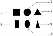
图中,1.结构层,2.衬底层,3.网格,4.刻蚀单元,5.正方形刻蚀孔,6.长方形刻蚀孔,7.圆形刻蚀孔,8.正三角形刻蚀孔,9.不规则三角形刻蚀孔,10.椭圆形刻蚀孔。In the figure, 1. Structural layer, 2. Substrate layer, 3. Grid, 4. Etching unit, 5. Square etching hole, 6. Rectangular etching hole, 7. Circular etching hole, 8. Regular triangle Etching hole, 9. Irregular triangular etching hole, 10. Oval etching hole.
具体实施方式Detailed ways
下面结合附图和具体实施方式对本发明进行详细说明。The present invention will be described in detail below with reference to the accompanying drawings and specific embodiments.
本发明一种单元随机分布的全介质多带太赫兹超材料吸收器,包括衬底层2和结构层1,如图1所示,衬底层2和结构层1为一体的高掺杂硅材料,结构层1上均匀划分有若干网格3,网格3内均设置有若干刻蚀单元4。刻蚀单元4为正方形刻蚀孔5、长方形刻蚀孔6、圆形刻蚀孔7、正三角形刻蚀孔8、不规则三角形刻蚀孔9、椭圆形刻蚀孔10的一种或多种,任一网格3内不重叠、不紧贴地设置有若干刻蚀单元4。任一网格3内刻蚀单元4至少存在一部分刻蚀图样被划分到相邻的网格3中。衬底层2厚度大于110μm,衬底层2厚度小于300μm。结构层1厚度与衬底层2厚度之比大于1/6小于1/2。刻蚀单元4的刻蚀面积与网格3面积之比大于1/20,刻蚀单元4的刻蚀面积与网格3面积之比小于1/2。刻蚀单元4在网格3内随机分布,刻蚀单元4在网格3内不具备周期性。网格3不少于10个。网格3内的刻蚀单元4均相同。任一网格3内刻蚀单元4的几何特征均相同。An all-dielectric multi-band terahertz metamaterial absorber with randomly distributed units of the present invention includes a
如图2所示,本发明提供一种单元随机分布的全介质多带太赫兹超材料吸收器,其结构层1具有划分均匀的网格3分布,即不同网格分布内的刻蚀结构构成了结构层1,并不刻蚀网格,网格只是对刻蚀结构限定范围。划分的网格分布中每一网格尺寸相同,且在x方向长度与y方向的长度之比大于1/2小于2,y方向长度与x方向的长度之比大于1/2小于2。As shown in FIG. 2 , the present invention provides an all-dielectric multi-band terahertz metamaterial absorber with randomly distributed cells, wherein the structural layer 1 has a uniformly divided
如图3所示,本发明提供的一种单元随机分布的全介质多带太赫兹超材料吸收器,刻蚀单元结构在结构层每一网格内随机分布,网格内的随机单元采用相同的几何尺寸和几何特征,刻蚀单元结构相互不重叠、不紧贴,刻蚀单元结构至少存在一部分刻蚀图样被划分到网格中。As shown in FIG. 3 , the present invention provides an all-dielectric multi-band terahertz metamaterial absorber with randomly distributed units. The etched unit structure is randomly distributed in each grid of the structural layer, and the random units in the grid use the same The geometrical dimensions and geometrical features of the etched unit structures do not overlap and adhere to each other, and at least a part of the etched pattern of the etched unit structure is divided into grids.
如图4所示,本发明提供的一种单元随机分布的全介质多带太赫兹超材料吸收器,刻蚀单元结构面积小于1/20网格面积,所述的刻蚀单元结构包括圆形刻蚀孔7,正方形刻蚀孔5,正三角形刻蚀孔8,以及其他衍生出的长方形刻蚀孔6,椭圆形刻蚀孔10、不规则三角形刻蚀孔9等,以及其他均匀图样。As shown in FIG. 4 , the present invention provides an all-dielectric multi-band terahertz metamaterial absorber with randomly distributed cells. The area of the etched unit structure is less than 1/20 of the grid area, and the etched unit structure includes a
如图5所示,本发明一种单元随机分布的全介质多带太赫兹超材料吸收器在采用五种不同随机单元分布情况下,在太赫兹频段的吸收光谱,在0.8THz、1.5THz、2.2THz附近具有吸收率高、高品质因子特点的吸收峰,不同随机方式的相应光谱类似,保证了吸收特性的稳定,同时也增加了共振模式的丰富程度。As shown in FIG. 5 , an all-dielectric multi-band terahertz metamaterial absorber with randomly distributed units of the present invention adopts five different random unit distributions, and the absorption spectrum in the terahertz frequency band is 0.8THz, 1.5THz, The absorption peaks near 2.2THz have the characteristics of high absorption rate and high quality factor, and the corresponding spectra of different random modes are similar, which ensures the stability of the absorption characteristics and also increases the richness of the resonance modes.
本发明一种单元随机分布的全介质多带太赫兹超材料吸收器,具有能够在不同单元排布下保持稳定的吸收光谱特性,且吸收率高、吸收频点多,高品质因子的特点。吸收模式更加丰富多样,且能在不同随机条件下保持稳定的吸收光谱特性。The invention is an all-dielectric multi-band terahertz metamaterial absorber with random distribution of cells, which can maintain stable absorption spectrum characteristics under different cell arrangements, and has the characteristics of high absorption rate, many absorption frequency points and high quality factor. The absorption modes are more abundant and diverse, and can maintain stable absorption spectral characteristics under different random conditions.
Claims (2)
Priority Applications (1)
| Application Number | Priority Date | Filing Date | Title |
|---|---|---|---|
| CN202110234078.XA CN113161760B (en) | 2021-03-03 | 2021-03-03 | An all-dielectric multiband terahertz metamaterial absorber with randomly distributed cells |
Applications Claiming Priority (1)
| Application Number | Priority Date | Filing Date | Title |
|---|---|---|---|
| CN202110234078.XA CN113161760B (en) | 2021-03-03 | 2021-03-03 | An all-dielectric multiband terahertz metamaterial absorber with randomly distributed cells |
Publications (2)
| Publication Number | Publication Date |
|---|---|
| CN113161760A CN113161760A (en) | 2021-07-23 |
| CN113161760B true CN113161760B (en) | 2022-08-02 |
Family
ID=76883903
Family Applications (1)
| Application Number | Title | Priority Date | Filing Date |
|---|---|---|---|
| CN202110234078.XA Active CN113161760B (en) | 2021-03-03 | 2021-03-03 | An all-dielectric multiband terahertz metamaterial absorber with randomly distributed cells |
Country Status (1)
| Country | Link |
|---|---|
| CN (1) | CN113161760B (en) |
Families Citing this family (1)
| Publication number | Priority date | Publication date | Assignee | Title |
|---|---|---|---|---|
| KR102906633B1 (en) * | 2021-11-03 | 2025-12-30 | 삼성전자주식회사 | Atypical metasurface, method of designing the same, waveguide image combiner using the atypical Metasurface, and augmented reality device |
Citations (2)
| Publication number | Priority date | Publication date | Assignee | Title |
|---|---|---|---|---|
| CN104360424A (en) * | 2014-10-19 | 2015-02-18 | 北京工业大学 | Broadband terahertz metamaterial absorber based on L-shaped structures |
| CN105896098A (en) * | 2016-04-25 | 2016-08-24 | 中国工程物理研究院激光聚变研究中心 | Broadband THz metamaterial absorber based on multi-resonant absorption superposition |
Family Cites Families (9)
| Publication number | Priority date | Publication date | Assignee | Title |
|---|---|---|---|---|
| EP1849621B1 (en) * | 2000-01-21 | 2014-04-16 | JDS Uniphase Corporation | Optically variable security devices |
| CN110167255A (en) * | 2013-03-15 | 2019-08-23 | 伟创力有限责任公司 | Method and apparatus for creating complete microwave absorption printed circuit board |
| IL277882B2 (en) * | 2018-04-16 | 2025-10-01 | Romy M Fain | Fabrication methods, structures, and uses for passive radiative cooling |
| CN109066095B (en) * | 2018-07-23 | 2020-08-04 | 西安理工大学 | A kind of fabricating method of broadband tunable terahertz wave absorber |
| CN110398793B (en) * | 2019-04-02 | 2021-05-25 | 西安理工大学 | All-dielectric-based optically-tunable dual-band terahertz absorber and manufacturing method thereof |
| CN110048239A (en) * | 2019-06-05 | 2019-07-23 | 中国计量大学 | A kind of light modulation Terahertz broadband wave absorbing device based on doped silicon |
| CN110265791B (en) * | 2019-06-19 | 2020-12-29 | 西安理工大学 | An optically tunable high-Q terahertz absorber based on a composite all-dielectric |
| CN111403922A (en) * | 2020-03-31 | 2020-07-10 | 苏州科技大学 | A kind of preparation method of broadband tunable perfect absorber and perfect absorber |
| CN112382858B (en) * | 2020-10-23 | 2022-03-15 | 西安理工大学 | Light-adjustable four-frequency-band terahertz metamaterial absorber based on all-dielectric material |
-
2021
- 2021-03-03 CN CN202110234078.XA patent/CN113161760B/en active Active
Patent Citations (2)
| Publication number | Priority date | Publication date | Assignee | Title |
|---|---|---|---|---|
| CN104360424A (en) * | 2014-10-19 | 2015-02-18 | 北京工业大学 | Broadband terahertz metamaterial absorber based on L-shaped structures |
| CN105896098A (en) * | 2016-04-25 | 2016-08-24 | 中国工程物理研究院激光聚变研究中心 | Broadband THz metamaterial absorber based on multi-resonant absorption superposition |
Also Published As
| Publication number | Publication date |
|---|---|
| CN113161760A (en) | 2021-07-23 |
Similar Documents
| Publication | Publication Date | Title |
|---|---|---|
| Yuan et al. | Wideband high-absorption electromagnetic absorber with chaos patterned surface | |
| CN103490169B (en) | Individual layer broadband random surface | |
| CN111883936B (en) | Terahertz electromagnetic absorber based on metamaterial | |
| CN211123332U (en) | Graphene-based broadband adjustable terahertz wave absorber | |
| CN102682858B (en) | Wave-absorbing material | |
| CN112739186B (en) | Metamaterial wave-absorbing structure for enhancing absorption and reducing surface radiation | |
| CN111755833B (en) | Multiband active metamaterial wave absorber | |
| CN111273384A (en) | An ultra-broadband absorber in the ultraviolet-visible-near-infrared band | |
| CN112332107A (en) | A Metal-Dielectric-Graphene Structured Metasurface Terahertz Broadband Absorber | |
| CN113036444A (en) | Polarization-insensitive metamaterial dual-frequency terahertz absorber | |
| CN110658571A (en) | A graphene-based broadband tunable terahertz absorber | |
| CN102778708A (en) | Optical-band wave absorber | |
| CN113161760B (en) | An all-dielectric multiband terahertz metamaterial absorber with randomly distributed cells | |
| CN111525272B (en) | Broadband terahertz absorber based on three "dart"-shaped graphene | |
| CN110534908A (en) | A kind of Meta Materials transparent microwave absorber of composite stereo formula ultra-wide band | |
| CN108539432B (en) | A terahertz wave absorbing device, wave absorbing unit and manufacturing method thereof | |
| CN214849067U (en) | Broadband terahertz wave absorber | |
| CN112072323A (en) | A terahertz switch based on metal and vanadium dioxide | |
| Zhang et al. | Comprehensive evaluation factor of optoelectronic properties for transparent conductive metallic mesh films | |
| Masuminia et al. | A novel tunable graphene based terahertz absorber with polarization insensitive | |
| CN110716247B (en) | A metamaterial selective absorber with high reflectivity in visible light and high absorption in the mid-infrared. | |
| CN211126084U (en) | Graphene-adjustable dual-band metamaterial absorber | |
| CN114784516A (en) | A realization method of a four-band terahertz absorber based on metamaterials | |
| CN107706539A (en) | A kind of single resonance device Meta Materials multi-band wave absorber of terahertz wave band | |
| CN210779001U (en) | A rhombus-shaped broadband terahertz absorber based on all-silicon material |
Legal Events
| Date | Code | Title | Description |
|---|---|---|---|
| PB01 | Publication | ||
| PB01 | Publication | ||
| SE01 | Entry into force of request for substantive examination | ||
| SE01 | Entry into force of request for substantive examination | ||
| GR01 | Patent grant | ||
| GR01 | Patent grant |