CN113140562A - Semiconductor structure - Google Patents
Semiconductor structure Download PDFInfo
- Publication number
- CN113140562A CN113140562A CN202110053725.7A CN202110053725A CN113140562A CN 113140562 A CN113140562 A CN 113140562A CN 202110053725 A CN202110053725 A CN 202110053725A CN 113140562 A CN113140562 A CN 113140562A
- Authority
- CN
- China
- Prior art keywords
- layer
- dielectric layer
- contact
- silicon
- oxide
- Prior art date
- Legal status (The legal status is an assumption and is not a legal conclusion. Google has not performed a legal analysis and makes no representation as to the accuracy of the status listed.)
- Pending
Links
Images


Classifications
-
- H10W20/0698—
-
- H—ELECTRICITY
- H10—SEMICONDUCTOR DEVICES; ELECTRIC SOLID-STATE DEVICES NOT OTHERWISE PROVIDED FOR
- H10D—INORGANIC ELECTRIC SEMICONDUCTOR DEVICES
- H10D84/00—Integrated devices formed in or on semiconductor substrates that comprise only semiconducting layers, e.g. on Si wafers or on GaAs-on-Si wafers
- H10D84/80—Integrated devices formed in or on semiconductor substrates that comprise only semiconducting layers, e.g. on Si wafers or on GaAs-on-Si wafers characterised by the integration of at least one component covered by groups H10D12/00 or H10D30/00, e.g. integration of IGFETs
- H10D84/82—Integrated devices formed in or on semiconductor substrates that comprise only semiconducting layers, e.g. on Si wafers or on GaAs-on-Si wafers characterised by the integration of at least one component covered by groups H10D12/00 or H10D30/00, e.g. integration of IGFETs of only field-effect components
- H10D84/83—Integrated devices formed in or on semiconductor substrates that comprise only semiconducting layers, e.g. on Si wafers or on GaAs-on-Si wafers characterised by the integration of at least one component covered by groups H10D12/00 or H10D30/00, e.g. integration of IGFETs of only field-effect components of only insulated-gate FETs [IGFET]
- H10D84/834—Integrated devices formed in or on semiconductor substrates that comprise only semiconducting layers, e.g. on Si wafers or on GaAs-on-Si wafers characterised by the integration of at least one component covered by groups H10D12/00 or H10D30/00, e.g. integration of IGFETs of only field-effect components of only insulated-gate FETs [IGFET] comprising FinFETs
-
- H10W20/435—
-
- H—ELECTRICITY
- H10—SEMICONDUCTOR DEVICES; ELECTRIC SOLID-STATE DEVICES NOT OTHERWISE PROVIDED FOR
- H10D—INORGANIC ELECTRIC SEMICONDUCTOR DEVICES
- H10D30/00—Field-effect transistors [FET]
- H10D30/01—Manufacture or treatment
- H10D30/021—Manufacture or treatment of FETs having insulated gates [IGFET]
- H10D30/024—Manufacture or treatment of FETs having insulated gates [IGFET] of fin field-effect transistors [FinFET]
-
- H—ELECTRICITY
- H10—SEMICONDUCTOR DEVICES; ELECTRIC SOLID-STATE DEVICES NOT OTHERWISE PROVIDED FOR
- H10D—INORGANIC ELECTRIC SEMICONDUCTOR DEVICES
- H10D30/00—Field-effect transistors [FET]
- H10D30/60—Insulated-gate field-effect transistors [IGFET]
- H10D30/62—Fin field-effect transistors [FinFET]
- H10D30/6211—Fin field-effect transistors [FinFET] having fin-shaped semiconductor bodies integral with the bulk semiconductor substrates
-
- H—ELECTRICITY
- H10—SEMICONDUCTOR DEVICES; ELECTRIC SOLID-STATE DEVICES NOT OTHERWISE PROVIDED FOR
- H10D—INORGANIC ELECTRIC SEMICONDUCTOR DEVICES
- H10D30/00—Field-effect transistors [FET]
- H10D30/60—Insulated-gate field-effect transistors [IGFET]
- H10D30/62—Fin field-effect transistors [FinFET]
- H10D30/6219—Fin field-effect transistors [FinFET] characterised by the source or drain electrodes
-
- H—ELECTRICITY
- H10—SEMICONDUCTOR DEVICES; ELECTRIC SOLID-STATE DEVICES NOT OTHERWISE PROVIDED FOR
- H10D—INORGANIC ELECTRIC SEMICONDUCTOR DEVICES
- H10D64/00—Electrodes of devices having potential barriers
- H10D64/01—Manufacture or treatment
- H10D64/021—Manufacture or treatment using multiple gate spacer layers, e.g. bilayered sidewall spacers
-
- H—ELECTRICITY
- H10—SEMICONDUCTOR DEVICES; ELECTRIC SOLID-STATE DEVICES NOT OTHERWISE PROVIDED FOR
- H10D—INORGANIC ELECTRIC SEMICONDUCTOR DEVICES
- H10D64/00—Electrodes of devices having potential barriers
- H10D64/20—Electrodes characterised by their shapes, relative sizes or dispositions
- H10D64/27—Electrodes not carrying the current to be rectified, amplified, oscillated or switched, e.g. gates
- H10D64/311—Gate electrodes for field-effect devices
- H10D64/411—Gate electrodes for field-effect devices for FETs
- H10D64/511—Gate electrodes for field-effect devices for FETs for IGFETs
- H10D64/517—Gate electrodes for field-effect devices for FETs for IGFETs characterised by the conducting layers
-
- H—ELECTRICITY
- H10—SEMICONDUCTOR DEVICES; ELECTRIC SOLID-STATE DEVICES NOT OTHERWISE PROVIDED FOR
- H10D—INORGANIC ELECTRIC SEMICONDUCTOR DEVICES
- H10D84/00—Integrated devices formed in or on semiconductor substrates that comprise only semiconducting layers, e.g. on Si wafers or on GaAs-on-Si wafers
- H10D84/01—Manufacture or treatment
- H10D84/0123—Integrating together multiple components covered by H10D12/00 or H10D30/00, e.g. integrating multiple IGBTs
- H10D84/0126—Integrating together multiple components covered by H10D12/00 or H10D30/00, e.g. integrating multiple IGBTs the components including insulated gates, e.g. IGFETs
- H10D84/0149—Manufacturing their interconnections or electrodes, e.g. source or drain electrodes
-
- H—ELECTRICITY
- H10—SEMICONDUCTOR DEVICES; ELECTRIC SOLID-STATE DEVICES NOT OTHERWISE PROVIDED FOR
- H10D—INORGANIC ELECTRIC SEMICONDUCTOR DEVICES
- H10D84/00—Integrated devices formed in or on semiconductor substrates that comprise only semiconducting layers, e.g. on Si wafers or on GaAs-on-Si wafers
- H10D84/01—Manufacture or treatment
- H10D84/0123—Integrating together multiple components covered by H10D12/00 or H10D30/00, e.g. integrating multiple IGBTs
- H10D84/0126—Integrating together multiple components covered by H10D12/00 or H10D30/00, e.g. integrating multiple IGBTs the components including insulated gates, e.g. IGFETs
- H10D84/0158—Integrating together multiple components covered by H10D12/00 or H10D30/00, e.g. integrating multiple IGBTs the components including insulated gates, e.g. IGFETs the components including FinFETs
-
- H—ELECTRICITY
- H10—SEMICONDUCTOR DEVICES; ELECTRIC SOLID-STATE DEVICES NOT OTHERWISE PROVIDED FOR
- H10D—INORGANIC ELECTRIC SEMICONDUCTOR DEVICES
- H10D84/00—Integrated devices formed in or on semiconductor substrates that comprise only semiconducting layers, e.g. on Si wafers or on GaAs-on-Si wafers
- H10D84/01—Manufacture or treatment
- H10D84/02—Manufacture or treatment characterised by using material-based technologies
- H10D84/03—Manufacture or treatment characterised by using material-based technologies using Group IV technology, e.g. silicon technology or silicon-carbide [SiC] technology
- H10D84/038—Manufacture or treatment characterised by using material-based technologies using Group IV technology, e.g. silicon technology or silicon-carbide [SiC] technology using silicon technology, e.g. SiGe
-
- H10P14/412—
-
- H10P50/283—
-
- H10P52/403—
-
- H10W20/056—
-
- H10W20/069—
-
- H10W20/0693—
-
- H10W20/077—
-
- H10W20/081—
-
- H10W20/432—
-
- H—ELECTRICITY
- H10—SEMICONDUCTOR DEVICES; ELECTRIC SOLID-STATE DEVICES NOT OTHERWISE PROVIDED FOR
- H10D—INORGANIC ELECTRIC SEMICONDUCTOR DEVICES
- H10D30/00—Field-effect transistors [FET]
- H10D30/60—Insulated-gate field-effect transistors [IGFET]
- H10D30/62—Fin field-effect transistors [FinFET]
-
- H—ELECTRICITY
- H10—SEMICONDUCTOR DEVICES; ELECTRIC SOLID-STATE DEVICES NOT OTHERWISE PROVIDED FOR
- H10D—INORGANIC ELECTRIC SEMICONDUCTOR DEVICES
- H10D64/00—Electrodes of devices having potential barriers
- H10D64/01—Manufacture or treatment
- H10D64/017—Manufacture or treatment using dummy gates in processes wherein at least parts of the final gates are self-aligned to the dummy gates, i.e. replacement gate processes
-
- H10P95/062—
Landscapes
- Engineering & Computer Science (AREA)
- Physics & Mathematics (AREA)
- Computer Hardware Design (AREA)
- Condensed Matter Physics & Semiconductors (AREA)
- General Physics & Mathematics (AREA)
- Microelectronics & Electronic Packaging (AREA)
- Power Engineering (AREA)
- Manufacturing & Machinery (AREA)
- Chemical & Material Sciences (AREA)
- Internal Circuitry In Semiconductor Integrated Circuit Devices (AREA)
- Chemical Kinetics & Catalysis (AREA)
- General Chemical & Material Sciences (AREA)
- Inorganic Chemistry (AREA)
- Geometry (AREA)
- Insulated Gate Type Field-Effect Transistor (AREA)
Abstract
The present disclosure provides a semiconductor structure. The semiconductor structure comprises a metal grid structure arranged above the semiconductor substrate; a gate spacer disposed on a sidewall of the metal gate structure; a source/drain contact disposed over the semiconductor substrate and separated from the metal gate structure by a gate spacer; and a contact member coupling the metal gate structure to the source/drain contact. The contact feature may be provided to include a dielectric layer disposed on a metal layer, wherein the dielectric layer and the metal layer are defined by continuous sidewalls.
Description
Technical Field
Embodiments of the present invention relate to a semiconductor structure, and more particularly, to a semiconductor device having a contact.
Background
The Integrated Circuit (IC) industry has experienced exponential growth. Technological advances in IC materials and design have resulted in generations of ICs where each generation has smaller and more complex circuits than the previous generation. In the course of IC evolution, the functional density (i.e., the number of interconnect devices per unit of chip area) is generally increased, while the geometry (i.e., the smallest component (or line) that can be produced using the process) is decreased. This scaling down process generally provides benefits by increasing production efficiency and reducing associated costs. This miniaturization has also increased the complexity of processing and manufacturing ICs
For example, as component dimensions continue to decrease, the fabrication of abutting contacts and interconnect components becomes more challenging. At smaller length scales, the abutting contacts and the interconnect features may benefit from extended separation distances to address electrical shorting issues and improve device performance. While existing methods of making abutting contacts and interconnect components are generally adequate, they are not satisfactory in all respects.
Disclosure of Invention
Embodiments of the present invention are directed to a semiconductor structure to solve at least one of the problems described above.
An embodiment of the present invention provides a semiconductor structure, including: a metal gate structure (MG) disposed over the semiconductor substrate; a gate spacer disposed on a sidewall of the metal gate structure; a source/drain contact (MD) disposed over the semiconductor substrate and separated from the metal gate structure by a gate spacer; and a contact member coupling the metal gate structure to the source/drain contact, wherein the contact member comprises a dielectric layer disposed on the metal layer, and wherein the dielectric layer and the metal layer are defined by continuous sidewalls.
An embodiment of the present invention provides a semiconductor structure, including: a metal gate stack disposed over the substrate; a source/drain (S/D) feature disposed over the substrate and adjacent to the metal gate stack; a source/drain contact disposed on the source/drain feature; a first interlayer dielectric (ILD) layer disposed over the source/drain contact; a butted contact (pressed contact) disposed in the first interlayer dielectric, wherein the butted contact extends from the first interlayer dielectric to the contact metal gate stack and the source/drain contact; a dielectric layer disposed on the contact, wherein a sidewall of the dielectric layer is defined by the first interlayer dielectric layer; a second interlayer dielectric layer disposed over the first interlayer dielectric layer; and a conductive member disposed in the second interlayer dielectric layer.
The embodiment of the invention provides a method for forming a semiconductor structure, which comprises the following steps: forming a semiconductor device including disposing a metal gate structure (MG) over the semiconductor layer, disposing a gate spacer on a sidewall of the MG, and disposing a source/drain (S/D) feature in the semiconductor layer and adjacent to the MG; forming source/drain contacts (MD) over the source/drain features; forming a first interlayer dielectric (ILD) layer over the metal gate structure and the source/drain contact; patterning the first interlayer dielectric layer to form an opening; forming a metal layer in the opening such that the metal layer contacts the metal gate structure and the source/drain contact; removing the top of the metal layer to form a groove; forming a dielectric layer over the remaining portion of the metal layer, thereby filling the trench; and forming a second interlayer dielectric layer on the dielectric layer.
Drawings
Aspects of the present disclosure are best understood from the following detailed description when read with the accompanying drawing figures. It should be emphasized that, in accordance with the standard practice in the industry, various features are not drawn to scale and are used for illustrative purposes only. In fact, the dimensions of the various elements may be arbitrarily increased or reduced for clarity of discussion.
Fig. 1 is a flow chart illustrating a method of manufacturing a semiconductor device according to aspects of the present disclosure.
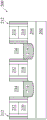
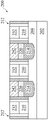
Fig. 2A is a perspective three-dimensional view of an embodiment of a semiconductor device, in accordance with aspects of the present disclosure.
Fig. 2B is a top plan view illustrating an embodiment of a semiconductor device, in accordance with aspects of the present disclosure.
Fig. 3, 4, 5, 6, 7, 8, 9, 10,11, 12, 13, 14, 15, 16, 17, 18, 19A, 19B, and 19C are cross-sectional views of the semiconductor device embodiment of fig. 2A and/or 2B along line a-a' during an intermediate step of the method embodiment of fig. 1, in accordance with aspects of the present disclosure.
The reference numbers are as follows:
100: method of producing a composite material
102,104,106,108,110,112,114,116,118,120: operation of
200: semiconductor device with a plurality of semiconductor chips
202: substrate
204: fin plate
208: isolation structure
210: HKMG structure
212: gate spacer
212A: first layer
212B: second layer
214: S/D component
218: ILD layer
220: S/D contact
230: groove
232: dielectric layer
234: groove
240: groove
242: dielectric layer
246:ESL
250: ILD layer
264: patterned mask element
266: patterned mask element
270A: first opening
270B: second opening
270C: opening of the container
280: abutting contact piece
282: opening of the container
284: dielectric layer
290:ESL
292: ILD layer
294: groove
296: internal connection structure
W': width of HKMG structure 210
W1: width of opening 270A
W2: width of opening 270B
T: thickness of
T': separation distance
H: total thickness of
A-A': thread
Detailed Description
The following provides many different embodiments, or examples, for implementing different features of embodiments of the invention. Specific examples of components and arrangements are described below to simplify the present disclosure. These are, of course, merely examples and are not intended to limit embodiments of the invention. For example, reference in the following description to forming a first member over or on a second member may include embodiments in which the first and second members are formed in direct contact, and may include embodiments in which additional members are formed between the first and second members, such that the first and second members may not be in direct contact. Also, spatially relative terms, such as "lower," "upper," "horizontal," "vertical," "above … …," "above … …," "below … …," "below … …," "above," "below," "top," "bottom," and the like, as well as derivatives thereof (e.g., "horizontally," "downwardly," "upwardly," etc.), may be used in order to describe a relationship of one element to another element in the disclosure. Spatially relative terms are intended to encompass different orientations of the device in which the component is embodied.
Further, when a number or range of numbers is described using the terms "about," "about," etc., the terms are intended to generally include the number within the reasonable range of the number, e.g., within +/-10% of the number described, or other values as would be understood by one of skill in the art. For example, the term "about 5 nm" summarizes the size range from 4.5nm to 5.5 nm.
Still further, examples of the present disclosure may use repeated reference symbols and/or wording. These repeated symbols or words are provided for simplicity and clarity and are not intended to limit the relationship between the embodiments and/or the configuration.
The present disclosure relates generally to semiconductor devices, and more particularly to field-effect transistors (FETs), such as planar FETs, three-dimensional fin-field-effect transistors (FinFETs), or gate-all-around (GAA) FETs. It is an object of the present disclosure to provide vertical interconnect features (e.g., wire contact features) for connecting source/drain contacts, metal gate stacks, and/or other features with additional interconnect features in a semiconductor device.
In FET fabrication, interconnect structures, such as conductive lines, may be formed proximate to an abutting contact that electrically couples a metal gate stack (e.g., a high-k metal gate or HKMG structure) to a source/drain (S/D) contact. At large length scales, the IC layout can be designed to ensure that the interconnect structures are sufficiently far from the abutting contacts to avoid potential electrical shorts between the two. However, as component sizes continue to decrease, accommodating such spacing becomes challenging. The present disclosure provides methods for reducing the spacing distance between interconnect structures and abutting contacts to mitigate potential electronic shorting concerns within the device.
Fig. 1 illustrates an embodiment of a method 100 of forming a semiconductor device 200 in accordance with aspects of the present disclosure. The method 100 is merely an example and is not intended to limit the present disclosure except as may be explicitly recited in the claims. Additional operations may be provided before, during, and after the method 100, and some operations may be replaced, removed, or moved for additional embodiments of the method. The method 100 is described below in conjunction with fig. 2A-19C, which are described above with respect to fig. 2A-19C of a portion of the semiconductor device 200 during intermediate steps of the method 100. Fig. 3-19C are cross-sectional views of the device 200 taken along the dashed line a-a' of fig. 2A and/or 2B. The device 200 may be an intermediate device or a portion thereof fabricated during the IC process, and the IC may include Static Random Access Memory (SRAM) and/or other logic circuits, passive components such as resistors, capacitors, and inductors, and active components such as p-type FETs (PFETs), n-type FETs (NFETs), FinFETs, GAA FETs, metal-oxide semiconductor field effect transistors (MOSFETs), complementary metal-oxide semiconductor (CMOS) transistors, bipolar transistors, high voltage transistors, high frequency transistors, and/or other memory cells. The present disclosure is not limited to any particular number of devices or device regions or any particular device configuration. For example, although the device 200 is shown as a three-dimensional FinFET device, the present disclosure may also provide embodiments for fabricating planar FET devices.
In operation 102, referring to fig. 2A, 2B, and 3, the method 100 provides a device 200 including a substrate 202, the substrate 202 having a three-dimensional active region 204 (hereinafter fin 204) disposed thereon. The device 200 further includes a high-k metal gate (HKMG) structure 210 disposed over the fins 204; a gate spacer 212 disposed on sidewalls of the HKMG structure 210; a source/drain (S/D) component 214 disposed over the fin 204; an isolation structure 208 disposed over the substrate 202 to separate various components of the device 200; and an interlayer dielectric (ILD) layer 218 disposed over the isolation structures 208 and the S/D features 214. As shown in fig. 2A and 2B, there are two fins 204 in the device 200. However, for clarity, the method of the present disclosure will be discussed with reference to one of the two fins 204; of course, the present disclosure is equally applicable to the other of the two fins 204.
The substrate 202 may include elemental (single element) semiconductors, such as silicon, germanium, and/or other suitable materials, compound semiconductors, and alloy semiconductors; such compound semiconductors as silicon carbide, gallium arsenide, gallium phosphide, indium arsenide, indium antimonide, and/or other suitable materials; such as SiGe, GaAsP, AlInAs, AlGaAs, GaInAs, GaInP, GaInAsP, and/or other suitable materials. The substrate 202 may be a single layer of material having a uniform composition. Alternatively, the substrate 202 may include multiple layers of materials having a composition similar to or different from a composition suitable for fabricating IC devices. In one example, the substrate 202 may be a silicon-on-insulator (SOI) substrate having a silicon layer formed on a silicon oxide layer. In another example, the substrate 202 may include conductive layers, semiconductor layers, dielectric layers, other layers, or combinations thereof.
In some embodiments where the substrate 202 includes FETs, various doped regions are formed in the substrate 202 or on the substrate 202. The doped region may be doped with an n-type dopant, such as phosphorus or arsenic, and/or a p-type dopant, such as boron or BF, depending on design requirements2. The doped region may be formed on the substrate 202 directly in a p-well structure, an n-well structure, a double-well structure, or using a raised structure. The doped regions may be formed by implantation of dopant atoms, epitaxial growth with in-situ doping, and/or other suitable techniques.
Still referring to fig. 2A, 2B, and 3, the fin 204 is suitable for forming a p-type or n-type FinFET. The fins 204 may be fabricated using suitable processes including photolithography and etching processes. The optical lithography process may include: a photoresist layer (resist) is formed over the substrate 202, the resist is exposed to a pattern, a post-exposure bake process is performed, and the resist is developed to form a mask element (not shown) including the resist. The mask elements are then used to etch recesses into the substrate 202, leaving the fins 204 on the substrate 202. The etching process may include dry etching, wet etching, Reactive Ion Etching (RIE), and/or other suitable processes.
Various other embodiments of the method for forming the fins 204 may be suitable. For example, the fin 204 may be patterned using a double patterning or multiple patterning process. In general, double patterning or multiple patterning processes combine lithographic processes with self-aligned processes to create patterns with, for example, a smaller pitch than would be obtained using a single, direct lithographic process. For example, in one embodiment, a sacrificial layer is formed over a substrate and patterned using a photolithographic process. Spacers are formed alongside the patterned sacrificial layer using a self-aligned process. The sacrificial layer is then removed and the remaining spacers or mandrels can then be used as a mask to pattern the fins.
The isolation structures 208 may comprise silicon oxide, silicon nitride, silicon oxynitride, fluorine-doped silicate glass (FSG), low-k dielectric materials, and/or other suitable materials. The isolation structure 208 may include a Shallow Trench Isolation (STI) feature. In one embodiment, the isolation structures 208 are formed by etching trenches in the substrate 202 during the formation of the fins 204. The trench may then be filled with the above-described isolation material by a deposition process followed by a chemical mechanical planarization/polishing (CMP) process. Other isolation structures such as field oxide, local oxidation of silicon (LOCOS), and/or other suitable structures may also be implemented as the isolation structures 208. Alternatively, the isolation structure 208 may comprise a multi-layered structure, for example with one or more thermal oxide liners. The isolation structures 208 may be deposited by any suitable method, such as: chemical Vapor Deposition (CVD), Flow CVD (FCVD), spin-on-glass (SOG), other suitable methods, or combinations thereof.
With continued reference to fig. 2A, 2B, and 3, the device 200 includes an S/D member 214 disposed over the fin 204 and adjacent to the HKMG structure 210. The S/D features 214 may be formed by any suitable technique, such as an etching process followed by one or more epitaxial processes. In one embodiment, one or more etching processes are performed to remove portions of the fins 204 to form respective recesses therein (not shown). A cleaning (clean) process may be performed to clean the recess using a hydrofluoric acid (HF) solution and/or other suitable solutions. Subsequently, one or more epitaxial growth processes are performed to grow epitaxial features in the recesses. The S/D components 214 may be suitable for p-type FinFET devices (e.g., p-type epitaxial material) or, instead, n-type FinFET devices (e.g., n-type epitaxial material). The p-type epitaxial material may include one or more epitaxial layers of silicon germanium (epi SiGe) doped with p-type dopants, such as boron, germanium, indium, and/or other p-type dopants. The n-type epitaxial material may include one or more epitaxial layers of silicon (epi Si) doped with n-type dopants, such as arsenic, phosphorus, and/or other n-type dopants, or epitaxial layers of silicon carbon (epi SiC) doped with n-type dopants.
The device 200 also includes an HKMG structure 210 disposed over a portion of the fins 204 such that it is interposed between the S/D members 214. HKMG structure 210 includes a high-k dielectric layer (i.e., having a dielectric constant greater than silicon oxide; not shown) disposed over fin 204 and a metal gate electrode (not shown) disposed over the high-k dielectric layer. The metal gate electrode may further include at least one work function metal layer and a bulk conductive layer disposed thereon. The work function metal layer may be a p-type or n-type work function metal layer. Exemplary work function materials include TiN, TaN, ZrSi2、MoSi2、TaSi2、NiSi2Ti, Ag, TaAl, TaAlC, TiAlN, TaC, TaCN, TaSiN, Ru, Mo, Al, WN, Mn, Zr, other suitable work function materials, or combinations thereof. The bulk conductive layer may comprise Cu, W, Ru, Al, Co, other suitable materials, or combinations thereof. The HKMG structure 210 may further include other layers (not shown) such as an interfacial layer, a hardmask layer, a capping layer, a barrier layer, a seed layer, other suitable layers, or combinations thereof disposed between the fin 204 and the high-k dielectric layer. The layers of the HKMG structure 210 may be deposited by any suitable method, such as: chemical oxidation, thermal oxidation, Atomic Layer Deposition (ALD), CVD, Physical Vapor Deposition (PVD), electroplating, other suitable methods, or combinations thereof. A polishing process, such as CMP, may be performed to remove excess material from the top surface of the HKMG structure 210 to planarize the top surface of the device 200.
The device 200 also includes gate spacers 212 disposed on sidewalls of the HKMG structure 210. The gate spacer 212 may be a single layer structure or a multi-layer structure. In some examples, the gate spacer 212 is a multilayer structure having a first layer 212A disposed on sidewalls of the HKMG structure 210, and a second layer 212B disposed on the first layer 212A, as described herein. Of course, other configurations (e.g., only one spacer layer, more than two spacer layers, etc.) are also applicable to the present embodiment. Gate spacer 212 may include aluminum oxide (aluminum oxide), aluminum oxynitride (aluminum oxynitride), hafnium oxide (hafnium oxide), titanium oxide (titanium oxide), zirconium aluminum oxide (zirconium aluminum oxide), zinc oxide (zinc oxide), tantalum oxide (tantalum oxide), lanthanum oxide (lanthanum oxide), yttrium oxide (yttrium oxide), silicon oxynitride (silicon oxide), tantalum carbide (tantalum carbide), silicon nitride (silicon nitride), zirconium nitride (zirconium nitride), silicon carbide (silicon carbide), silicon oxide (silicon oxide), silicon carbide (silicon carbide), hafnium silicide (silicon carbide), silicon (silicon nitride), zirconium silicide (silicon silicide), zirconium silicide (zirconium silicide), other suitable materials, or combinations thereof. It should be noted that the composition of the gate spacers 212 is different from the composition of the surrounding dielectric elements, such that there is an etch selectivity between the gate spacers 212 and the surrounding dielectric elements during a subsequent etch process. The gate spacers 212 may be formed on the sidewalls of the HKMG structure 210 by first depositing a blanket layer of spacer material (a blanket of) over the device 200, and then performing an anisotropic etch process to remove portions of the spacer material.
In some embodiments, the HKMG structure 210 is formed after other components of the device 200 (e.g., the S/D components 214) are fabricated. This process, which is commonly referred to as a gate replacement process, includes forming dummy gate structures (not shown) as placeholders (spacers) for the HKMG structures 210, forming S/D features 214 adjacent to the dummy gate structures, forming an ILD layer 218 (and optionally an etch stop layer or ESL) over the dummy gate structures and S/D features 214, planarizing the ILD layer 218 by, for example, a CMP process to expose top surfaces of the dummy gate structures, removing the dummy gate structures in the ILD layer 218 to form gate trenches (not shown) exposing the channel regions of the fins 204, and forming the HKMG structures 210 in the gate trenches to complete the gate replacement process. In some embodiments, ILD layer 218 comprises dielectric materials such as: low-k dielectric materials, Tetraethoxysilane (TEOS), silicon oxide, doped silicon oxides such as the following, and other suitable dielectric materials or combinations thereof: borophosphosilicate glass (BPSG), fluoro-doped silicate glass (FSG), phosphosilicate glass (PSG), Bororoned Silicate Glass (BSG). ILD layer 218 may comprise a multilayer structure having a variety of dielectric materials and may be formed by, for example, the following deposition processes: CVD, FCVD, SOG, other suitable methods, or combinations thereof. If included, the ESL may include silicon nitride, silicon oxynitride, silicon nitride with oxygen or carbon elements, other suitable materials, or combinations thereof, and may be formed by CVD, PVD, ALD, other suitable methods, or combinations thereof.
Referring to fig. 4 and 5, the method 100 forms a dielectric layer 232 over the HKMG structure 210 at operation 104. Referring to fig. 4, the method 100 first removes portions of the HKMG structure 210 to form trenches 230. In some embodiments, the method 100 performs an etching process, such as a dry etching process, to form the trench 230. The etching process selectively removes HKMG structure 210 relative to ILD layer 218 such that ILD layer 218 is not etched or is only minimally etched. Referring to fig. 5, the method 100 continues by forming a dielectric layer 232 in the trench 230. In the present embodiment, the method 100 deposits the dielectric material by, for example, the following suitable methods: CVD, FCVD, ALD, PVD, other suitable methods, or combinations thereof. Dielectric layer 232 may comprise silicon oxide (silicon oxide), silicon nitride (silicon nitride), silicon carbide (silicon carbide), silicon nitride (silicon carbide), silicon oxynitride (silicon oxynitride), silicon oxycarbide (silicon oxycarbide), aluminum oxide (aluminum oxide), aluminum nitride (aluminum nitride), aluminum oxynitride (aluminum oxynitride), zirconium oxide (zirconium oxide), zirconium nitride (zirconium nitride), zirconium aluminum oxide (zirconium aluminum oxide), hafnium oxide (hafnium oxide), other suitable materials, or combinations thereof. In the present embodiment, the composition of the dielectric layer 232 is different from the composition of the gate spacers 212. The method 100 then planarizes the top surface of the device 200 using a suitable method, such as CMP, to expose the top surface of the ILD layer 218. In some embodiments, the CMP process results in the top surface of dielectric layer 232 being substantially coplanar with the top surfaces of ILD layer 218 and gate spacers 212, as shown in figure 5. In some embodiments, the dielectric layer 232 and subsequently formed dielectric layer 242 are optional and may be omitted in the device 200.
Referring to fig. 6 and 7, the method 100 forms an S/D contact 220 over the S/D member 214 at operation 106. Referring to fig. 6, the method 100 removes portions of the ILD layer 218 disposed over the S/D features 214 to form trenches 234. The method 100 may implement any suitable etching process (e.g., dry etch, wet etch, RIE, etc.) to form the trench 234. In some embodiments, the etching process is a dry etching process that uses one or more etchants, such as C4F6Oxygen, hydrogen, other suitable gases, or combinations thereof. Referring to fig. 7, the method 100 then deposits a conductive material in the trench 234 and over portions of the dielectric layer 232. The conductive material may include Co, W, Ru, Cu, Ta, Ti, Al, Mo, other suitable materials, or combinations thereof. The conductive material may be deposited by any suitable method, such as: CVD, PVD, ALD, electroplating, other suitable methods, or combinations thereof. In some embodiments, a barrier layer (not shown) is formed in trench 234 prior to depositing the conductive material. The barrier layer may comprise TiN, TaN, other suitable materials, or combinations thereof, and may be deposited by, for example, an ALD process. Then, with continued reference to FIG. 7, the method 100 planarizes the conductive material using a suitable method, such as CMP, to form S/D contacts 220 over the S/D features 214. In some embodiments, the portion of the conductive material formed over the dielectric layer 232 is removed by a CMP process such that the top surface of the S/D contact is substantially coplanar with the top surface of the dielectric layer 232.
Referring to fig. 8 and 9, the method 100 forms a dielectric layer 242 over the dielectric layer 232 and the S/D contacts 220 at operation 108. In some embodiments, referring to fig. 8, the method 100 first removes portions of the S/D contacts 220 to form trenches 240 disposed between the gate spacers 212. The method 100 may implement any suitable etching process (e.g., dry etching, wet etching, RIE, etc.) to form the trench 240. In the present disclosure, the etching process may be a wet etching process using an acid, such as sulfuric acid (H), as an etchant2SO4). In some embodiments, the channelThe duration (duration) of the over-etch process controls the wet etch process. Referring to fig. 9, the method 100 then deposits a dielectric layer 242 in the trench 240 and over portions of the dielectric layer 232 using any suitable method, for example: CVD, FCVD, ALD, PVD, other suitable methods, or combinations thereof. The dielectric layer 242 may include silicon oxide (silicon oxide), silicon nitride (silicon nitride), silicon carbide (silicon carbide), silicon carbide nitride (silicon carbide), silicon oxynitride (silicon oxynitride), silicon oxycarbide (silicon oxycarbide), aluminum oxide (aluminum oxide), aluminum nitride (aluminum nitride), aluminum oxynitride (aluminum oxynitride), zirconium oxide (zirconium oxide), zirconium nitride (zirconium nitride), zirconium aluminum oxide (zirconium oxide), hafnium oxide (hafnium oxide), other suitable materials, or combinations thereof. It should be noted that dielectric layer 242 has a different composition than dielectric layer 232 and gate spacers 212 in the present disclosure, such that it will exhibit etch selectivity when subjected to a subsequent etch process. Then, with continued reference to fig. 9, the method 100 planarizes the top surface of the device 200 to expose the top surfaces of the dielectric layer 232 and the gate spacers 212 such that the top surface of the dielectric layer 242 is substantially coplanar with the top surface of the dielectric layer 232.
Referring to fig. 10-13, method 100 forms an opening 270C (shown in fig. 13) in ILD layer 250 at operation 110 to expose one of S/D contacts 220 and one of HKMG structures 210. Referring to fig. 10, method 100 first forms ESL 246 over device 200 and then forms ILD layer 250 thereover. In some embodiments, device 200 omits ESL 246. ESL 246 may comprise silicon oxide (silicon oxide), silicon nitride (silicon nitride), silicon carbide (silicon carbide), silicon nitride (silicon carbide), silicon oxynitride (silicon oxynitride), silicon oxycarbide (silicon oxycarbide), aluminum oxide (aluminum oxide), aluminum nitride (aluminum nitride), aluminum oxynitride (aluminum oxynitride), zirconium oxide (zirconium oxide), zirconium nitride (zirconium nitride), zirconium aluminum oxide (zirconium aluminum oxide), hafnium oxide (hafnium oxide), other suitable materials, or combinations thereof. It should be noted that gate spacer 212, dielectric layer 232, dielectric layer 242, and ESL 246 may have different compositions such that they may exhibit etch selectivity when subjected to one or more subsequent etch processes. In some embodiments, method 100 deposits ESL 246 using any suitable method, such as the following: CVD, ALD, other suitable methods, or combinations thereof. Method 100 then forms ILD layer 250 over ESL 246 using any suitable method, including: CVD, FCVD, SOG, other suitable methods, or combinations thereof. ILD layer 250 may have a composition similar to ILD layer 218 and may be formed by a process similar to that described above with respect to ILD layer 218. ILD layer 250 may comprise a multilayer structure having a plurality of dielectric materials.
Subsequently, the method 100 forms an opening 270C to expose a portion of the device 200. In the present disclosure, the opening 270C may be formed in two process steps or, alternatively, in a single process step. For example, referring to fig. 11 and 12, a first opening 270A and a second opening 270B are formed in the device 200, respectively. Referring to fig. 11, the method 100 begins by forming a patterned mask element 264 having an opening positioned to expose at least a portion of the S/D contact 220. Forming patterned mask elements 264 may include forming at least a resist layer (e.g., a photoresist layer; not shown) over device 200, exposing the resist layer to a radiation source (e.g., extreme ultraviolet or EUV radiation) through a photomask, and then developing the exposed resist layer to form patterned mask elements 264. The portion of the device 200 exposed by the patterned mask element 264 is then removed to expose at least a portion of the S/D contact 220 in the opening 270A. In the present embodiment, the composition of gate spacers 212 and/or a suitable etchant is selected such that gate spacers 212 are not etched or are only minimally etched with respect to ILD layer 250, ESL 246, and dielectric layer 242. The patterned mask element 264 is then removed from the apparatus 200 by, for example, the following suitable methods: resist stripping and/or plasma ashing. It is understood that fig. 11 is merely an example, and in some embodiments, the opening 270A may expose the entire S/D contact 220. In other words, the width W1 of the opening 270A may be as large as the width W of the S/D contact 220.
Subsequently, referring to fig. 12, a second opening 270B is formed adjacent to the first opening 270A to expose at least a portion of the HKMG structure 210. The method 100 may form the opening 270B in a similar manner as described above for the opening 270A. For example, a patterned mask element 266 may be formed over the device 200, and the first opening 270A may be refilled by the patterned mask element 266 during the above-described process. The portions of the device 200 exposed by the patterned mask elements 266 are then etched to expose at least a portion of the HKMG structure 210. In some embodiments, gate spacers 212 are not etched or minimally etched similar to that described above to form opening 270A. In the case of opening 270A, width W2 of opening 270B may be as large as width W' of HKMG structure 210.
Referring now to fig. 13, the patterned mask elements 266 are removed (by photoresist stripping and/or plasma ashing) resulting in openings 270C. As shown by the dashed lines and arrows, the openings 270C of the sidewalls may be expanded to align with the sidewalls of the S/D contacts 220 and HKMG structure 210. It should be understood that the opening 270C is configured to expose only one S/D contact 220 and one HKMG structure 210, the HKMG structure 210 being adjacent to the S/D contact, such that a pressed contact (e.g., the pressed contact 280 shown in fig. 14-19C) may be subsequently formed in the opening 270C. In an alternative embodiment, the opening 270C is formed in a single process step. For example, a patterned mask element (not shown) may be formed over ILD layer 250, wherein the patterned mask element is configured to expose at least portions of S/D contact 220 and HKMG structure 210. The device 200 exposed in the opening is then etched to form an opening 270C, after which the patterned mask element is removed from the device 200.
Referring now to fig. 14, method 100 forms an abutting contact 280 in opening 270C at operation 112. Forming the abutting contact 280 includes depositing a conductive material over the device 200, filling the opening 270C, and then planarizing the top surface of the device 200 to expose the ILD layer 250. In the present embodiment, the abutment contact 280 is configured to electrically connect the S/D contact 220 (i.e., the S/D component 214) to the HKMG structure 210. The abutting contact 280 may comprise any suitable conductive material such as: co, W, Ru, Cu, Ta, Ti, Al, Mo, other suitable conductive materials, or combinations thereof. In some embodiments, the composition of the abutment contact 280 is substantially similar or identical to the composition of the S/D contact 220. The conductive material may be deposited in the opening 270C by any suitable method, such as: CVD, PVD, electroplating, other suitable methods, or combinations thereof. In some embodiments, a barrier layer (not shown) is formed in opening 270C prior to forming abutting contact 280. The barrier layer may comprise TiN, TaN, other suitable materials, or combinations thereof, and may be deposited by, for example, an ALD process.
Subsequently, referring to fig. 15, the method 100 removes the top of the abutment contact 280 at operation 114 to form an opening 282. Due to the composition differences between ILD layer 250 and abutting contact 280, method 100 may selectively remove the top of abutting contact 280 relative to ILD layer 250 during the etching process without the use of a patterned masking layer. In other words, the etching process at operation 114 forms the opening 282 in a self-aligned manner. The etch process performed at operation 114 may be any suitable etch process such as: a dry etch process, a wet etch process, RIE, or a combination thereof. In the present embodiment, the etching process is performed by using a chlorine-containing gas (e.g., Cl)2、CHCl3、CCl4And/or BCl3) Dry etching process or RIE as an etchant. In some embodiments, the depth of the opening 282 is controlled by adjusting the duration of the etch process of operation 114. The depth of the opening 282 is not limited to a particular value in this embodiment, as long as it is less than the separation distance measured from the top surface of the ILD layer 250 to the top surface of the gate spacer 212, wherein the gate spacer 212 is used to separate adjacent S/D contacts 220 and HKMG structures 210. In other words, the top surface of the remaining portion of the abutment contact 280 should be sufficiently higher than the top surface of the gate spacer 212 so that the abutment contact 280 remains functional in electrically connecting the S/D contact 220 to the HKMG structure 210. In some examples, the depth of the opening 282 may be about 5nm to about 20 nm.
Subsequently, referring to fig. 16, the method 100 forms a dielectric layer 284 over the remaining portion of the abutting contact 280 at operation 116, filling the opening 282. Dielectric layer 284 may comprise silicon oxide (silicon oxide), silicon nitride (silicon nitride), silicon carbide (silicon carbide), silicon nitride carbide (silicon carbide), silicon oxynitride (silicon oxynitride), silicon oxycarbide (silicon oxycarbide), aluminum oxide (aluminum oxide), aluminum nitride (aluminum nitride), aluminum oxynitride (aluminum oxynitride), zirconium oxide (zirconium oxide), zirconium nitride (zirconium nitride), zirconium aluminum oxide (zirconium aluminum oxide), hafnium oxide (hafnium oxide), other suitable materials, or combinations thereof. Dielectric layer 284 may have a composition substantially similar or identical to dielectric layer 232, dielectric layer 242, and/or ESL 246. In other words, the composition of the dielectric layer 284 is not limited to be different from one or more of the dielectric layer 232, the dielectric layer 242, and the ESL 246. The method 100 may deposit the dielectric layer 284 using any suitable method, such as the following; ALD, CVD, FCVD, PVD, other suitable methods, or combinations thereof, and then a CMP process is performed to expose the top surface of ILD layer 250. In an exemplary embodiment, the dielectric layer 284 is deposited using an ALD process.
As discussed above with respect to the depth of the opening 282, the thickness T of the dielectric layer 284 should not exceed the separation distance T' between the top surface of the dielectric layer 284 and the top surface of the gate spacer 212 to ensure that the abutment contact 280 electrically connects the S/D contact 220 with the HKMG structure 210. In some embodiments, the ratio of the thickness T to the total thickness H of the dielectric layer 284 and the abutting contact 280 is at least about 1: 9 to ensure that the dielectric layer 284 provides adequate isolation between the abutting contact 280 and subsequently formed interconnect structures (e.g., interconnect structure 296, discussed in greater detail below). In some examples, the thickness T is about 5nm to about 15nm and the separation distance T' is about 10nm to about 30 nm. Of course, the present embodiment is not limited to these numerical ranges, and other numerical ranges may be applied as long as the functions of the dielectric layer 284 and the abutting contact 280 are properly maintained as described above.
Referring now to fig. 17-19C, the method 100 forms an interconnect structure 296 (as shown in fig. 19A-19C) over the ILD layer 250 at operation 118. Referring to fig. 17, the method 100 begins by forming an ESL 290 over the ILD layer 250 and forming an ILD layer 292 over the ESL 290. In some embodiments, device 200 omits ESL 290. The composition of ESL 290 may be similar to that of ESL 246, and ESL 290 may be deposited using any suitable method as discussed above with respect to ESL 246. ILD layer 292 may be similar to ILD layer 218 and/or ILD layer 250, and ILD layer 292 may be formed using any suitable method as discussed above with respect to ILD layer 218.
Referring to fig. 18, the method 100 then forms trenches 294 extending through the ILD layer 292 (and the ESL 290, if present). The trench 294 may be formed by a series of patterning and etching processes similar to those described above with respect to operation 110. For example, a patterned mask element (not shown) exposing portions of the ILD layer 292 and the ESL 290 may be formed over the ILD layer 250, and the exposed portions are then removed by a suitable etching process (e.g., a dry etching process) to form the trenches 294. The size of the trench 294 is not limited in this embodiment as long as it meets the design requirements for forming the interconnect structure therein. As will be discussed in detail below, the trench 294 may be formed at a location completely offset from the dielectric layer 284 as shown in fig. 18, such that it does not expose any portion of the dielectric layer 284; alternatively, the trench 294 may be configured to expose a portion of the dielectric layer 284 as shown by the dashed outline of the trench 294.
Referring to fig. 19A-19C, the method 100 deposits a conductive material in the trench 294 to form an interconnect structure 296. Interconnect structure 296 may be any structure suitable for interconnecting one or more components of device 200 with subsequently formed components. For example, the interconnect structure 296 may be a horizontal interconnect structure, such as a conductive line. It is understood that ILD layer 292 may include additional interconnect structures (e.g., vias, conductive lines, etc.) not shown herein. Further, it should be understood that the interconnect structure 296 may contact one or more components of the device 200 (e.g., gate contacts, S/D contacts, etc.) not shown herein. The interconnect structure 296 may include Co, W, Ru, Cu, Ta, Ti, Al, Mo, other suitable conductive materials, or combinations thereof, and may be deposited by any suitable method, such as: CVD, PVD, electroplating, other suitable methods, or combinations thereof. In some embodiments, a barrier layer (not shown) is formed in the trench 294 prior to forming the interconnect structure 296. The barrier layer may comprise TiN, TaN, other suitable materials, or combinations thereof, and may be deposited by, for example, an ALD process. After depositing the conductive material(s), the method 100 performs a CMP process to planarize the device 200, thereby exposing a top surface of the ILD layer 292. The method 100 may then perform additional process steps at operation 120, such as forming additional interconnect structures in the ILD layer 292 and/or forming additional ILD layers above the ILD layer 292 and subsequently forming additional interconnect structures therein.
With respect to the exemplary embodiment of fig. 19A, the interconnect structure 296 is laterally offset from the dielectric layer 284 by a distance L. If the abutting contact 280 extends vertically to contact the ESL 290, i.e., if the device 200 does not have the dielectric layer 284 present, the distance L must be kept at a minimum distance of about 5nm to prevent electrical shorting between the interconnect structure 296 and the abutting contact 280. Of course, such an arrangement will extend the lateral dimensions of the device 200, thereby limiting the density of the various components of the device 200.
In contrast, the presence of the dielectric layer 284 over the abutting contact 280, as shown in FIGS. 19B and 19C, eliminates the need to maintain the distance L, such that the interconnect structure 296 may laterally overlap the dielectric layer 284, as shown in FIG. 19B, or alternatively may be formed directly over the dielectric layer 284 (i.e., the bottom surface of the interconnect structure 296 is defined by the top surface of the dielectric layer 284). In other words, because shorting between the interconnect structure 296 and the abutting contact 280 may be prevented by interposing the dielectric layer 284, the lateral dimensions of the device 200 may be reduced and the density of various components in the device 200 may be improved. Furthermore, the insertion of the dielectric layer 284 between the contact 280 and the interconnect structure 296 may result in a reduction in the parasitic capacitance and resistance of the device 200, and may, in some examples, increase the speed of the device 200 by about 10%. In some examples, the composition of the dielectric layer 284 may be selected to adjust the degree of reduction in parasitic capacitance and/or resistance required for a particular design requirement. For the embodiments shown in fig. 19B and 19C, the compositions of the dielectric layer 284 and the ESL 290 are chosen to be different to ensure that there is sufficient etch selectivity between them when forming the trench 294 so that the dielectric layer 284 is not accidentally damaged.
Although not intended to be limiting, one or more embodiments of the present disclosure provide many benefits of semiconductor devices and their formation. For example, embodiments of the present disclosure provide a method comprising forming a contact comprising a dielectric layer disposed over a conductive layer, and then forming an interconnect structure over the contact. In some embodiments, the interconnect structure laterally overlaps a portion of the dielectric layer. In some embodiments, the interconnect structure is formed as a contact dielectric layer. Embodiments provided herein allow for the formation of interconnect structures in close proximity to abutting contacts to reduce the overall size of the device, increase the density of components in the device, and improve the performance of the device.
In one aspect, the present disclosure provides a semiconductor structure comprising: a metal gate structure (MG) disposed over the semiconductor substrate; a gate spacer disposed on a sidewall of the metal gate structure; a source/drain contact (MD) disposed over the semiconductor substrate and separated from the metal gate structure by a gate spacer; and a contact member coupling the metal gate structure to the source/drain contact. In this embodiment, the contact feature includes a dielectric layer disposed on a metal layer, and wherein the dielectric layer and the metal layer are defined by continuous sidewalls.
In another aspect, the present disclosure provides a semiconductor structure comprising: a metal gate stack disposed over the substrate; a source/drain (S/D) feature disposed over the substrate and adjacent to the metal gate stack; and the S/D contact piece is arranged on the S/D component. The semiconductor structure further includes a first interlayer dielectric (ILD) layer disposed over the S/D contact; a pressed contact (pressed contact) disposed in the first ILD layer; a dielectric layer disposed on the contact member; a second ILD layer disposed over the first ILD layer; and a conductive feature disposed in the second ILD layer. In this embodiment, the landing contact extends from the first ILD layer to the contact metal gate stack and the S/D contact, and the sidewalls of the dielectric layer are defined by the first ILD layer.
In yet another aspect, the present disclosure provides a method of forming a semiconductor structure, comprising: first, a metal gate structure is formed over a semiconductor layer, a gate spacer is disposed on a sidewall of the metal gate structure, a source/drain (S/D) feature is disposed in the semiconductor layer and adjacent to the metal gate structure, an S/D contact (MD) is formed over the S/D feature, an interlayer dielectric (ILD) layer is formed over the metal gate structure and the S/D contact, and then the first ILD layer is patterned to form an opening. The method further includes forming a metal layer in the opening such that the metal layer contacts the metal gate structure and the S/D contact, removing a top portion of the metal layer to form a trench, filling the trench with a dielectric layer, and then forming a second ILD layer over the dielectric layer.
The components of several embodiments are summarized above so that those skilled in the art to which the present invention pertains can more clearly understand the aspects of the embodiments of the present invention. Those skilled in the art should appreciate that they may readily use the present disclosure as a basis for designing or modifying other processes and structures for carrying out the same purposes and/or achieving the same advantages of the embodiments introduced herein. Those skilled in the art should also realize that such equivalent constructions do not depart from the spirit and scope of the present disclosure, and that they may make various changes, substitutions, and alterations herein without departing from the spirit and scope of the present disclosure.
Claims (1)
1. A semiconductor structure, comprising:
a metal gate structure disposed above a semiconductor substrate;
a gate spacer disposed on a sidewall of the metal gate structure;
a source/drain contact disposed above the semiconductor substrate and separated from the metal gate structure by the gate spacer; and
a contact member coupling the metal gate structure to the source/drain contact, wherein the contact member comprises a dielectric layer disposed on a metal layer, and wherein the dielectric layer and the metal layer are defined by continuous sidewalls.
Applications Claiming Priority (2)
| Application Number | Priority Date | Filing Date | Title |
|---|---|---|---|
| US16/745,716 US11244899B2 (en) | 2020-01-17 | 2020-01-17 | Butted contacts and methods of fabricating the same in semiconductor devices |
| US16/745,716 | 2020-01-17 |
Publications (1)
| Publication Number | Publication Date |
|---|---|
| CN113140562A true CN113140562A (en) | 2021-07-20 |
Family
ID=76810422
Family Applications (1)
| Application Number | Title | Priority Date | Filing Date |
|---|---|---|---|
| CN202110053725.7A Pending CN113140562A (en) | 2020-01-17 | 2021-01-15 | Semiconductor structure |
Country Status (3)
| Country | Link |
|---|---|
| US (3) | US11244899B2 (en) |
| CN (1) | CN113140562A (en) |
| TW (1) | TW202133323A (en) |
Families Citing this family (5)
| Publication number | Priority date | Publication date | Assignee | Title |
|---|---|---|---|---|
| US11437490B2 (en) * | 2020-04-08 | 2022-09-06 | Globalfoundries U.S. Inc. | Methods of forming a replacement gate structure for a transistor device |
| CN113782487B (en) * | 2020-06-10 | 2023-10-20 | 中芯国际集成电路制造(上海)有限公司 | Semiconductor structures and methods of forming them |
| KR102902367B1 (en) * | 2021-09-09 | 2025-12-18 | 삼성전자주식회사 | Semiconductor memory device |
| US12131945B2 (en) * | 2022-01-21 | 2024-10-29 | Taiwan Semiconductor Manufacturing Company, Ltd. | Semiconductor device and manufacturing method thereof |
| US20250081523A1 (en) * | 2023-08-29 | 2025-03-06 | Taiwan Semiconductor Manufacturing Co., Ltd. | Contacts in semiconductor devices and methods of forming the same |
Family Cites Families (27)
| Publication number | Priority date | Publication date | Assignee | Title |
|---|---|---|---|---|
| US9245805B2 (en) | 2009-09-24 | 2016-01-26 | Taiwan Semiconductor Manufacturing Company, Ltd. | Germanium FinFETs with metal gates and stressors |
| US8816444B2 (en) | 2011-04-29 | 2014-08-26 | Taiwan Semiconductor Manufacturing Company, Ltd. | System and methods for converting planar design to FinFET design |
| US8962400B2 (en) | 2011-07-07 | 2015-02-24 | Taiwan Semiconductor Manufacturing Company, Ltd. | In-situ doping of arsenic for source and drain epitaxy |
| US8841701B2 (en) | 2011-08-30 | 2014-09-23 | Taiwan Semiconductor Manufacturing Company, Ltd. | FinFET device having a channel defined in a diamond-like shape semiconductor structure |
| US8815712B2 (en) | 2011-12-28 | 2014-08-26 | Taiwan Semiconductor Manufacturing Company, Ltd. | Method for epitaxial re-growth of semiconductor region |
| US9236267B2 (en) | 2012-02-09 | 2016-01-12 | Taiwan Semiconductor Manufacturing Company, Ltd. | Cut-mask patterning process for fin-like field effect transistor (FinFET) device |
| US8847293B2 (en) | 2012-03-02 | 2014-09-30 | Taiwan Semiconductor Manufacturing Company, Ltd. | Gate structure for semiconductor device |
| US8785285B2 (en) | 2012-03-08 | 2014-07-22 | Taiwan Semiconductor Manufacturing Company, Ltd. | Semiconductor devices and methods of manufacture thereof |
| US8836016B2 (en) | 2012-03-08 | 2014-09-16 | Taiwan Semiconductor Manufacturing Company, Ltd. | Semiconductor structures and methods with high mobility and high energy bandgap materials |
| US8860148B2 (en) | 2012-04-11 | 2014-10-14 | Taiwan Semiconductor Manufacturing Company, Ltd. | Structure and method for FinFET integrated with capacitor |
| US9171929B2 (en) | 2012-04-25 | 2015-10-27 | Taiwan Semiconductor Manufacturing Company, Ltd. | Strained structure of semiconductor device and method of making the strained structure |
| US8823065B2 (en) | 2012-11-08 | 2014-09-02 | Taiwan Semiconductor Manufacturing Company, Ltd. | Contact structure of semiconductor device |
| US9105490B2 (en) | 2012-09-27 | 2015-08-11 | Taiwan Semiconductor Manufacturing Company, Ltd. | Contact structure of semiconductor device |
| US8772109B2 (en) | 2012-10-24 | 2014-07-08 | Taiwan Semiconductor Manufacturing Company, Ltd. | Apparatus and method for forming semiconductor contacts |
| US9236300B2 (en) | 2012-11-30 | 2016-01-12 | Taiwan Semiconductor Manufacturing Company, Ltd. | Contact plugs in SRAM cells and the method of forming the same |
| US9093530B2 (en) | 2012-12-28 | 2015-07-28 | Taiwan Semiconductor Manufacturing Company, Ltd. | Fin structure of FinFET |
| US8853025B2 (en) | 2013-02-08 | 2014-10-07 | Taiwan Semiconductor Manufacturing Company, Ltd. | FinFET/tri-gate channel doping for multiple threshold voltage tuning |
| US9093514B2 (en) | 2013-03-06 | 2015-07-28 | Taiwan Semiconductor Manufacturing Co., Ltd. | Strained and uniform doping technique for FINFETs |
| US9214555B2 (en) | 2013-03-12 | 2015-12-15 | Taiwan Semiconductor Manufacturing Co., Ltd. | Barrier layer for FinFET channels |
| US8963258B2 (en) | 2013-03-13 | 2015-02-24 | Taiwan Semiconductor Manufacturing Company | FinFET with bottom SiGe layer in source/drain |
| US8796666B1 (en) | 2013-04-26 | 2014-08-05 | Taiwan Semiconductor Manufacturing Company, Ltd. | MOS devices with strain buffer layer and methods of forming the same |
| US9136106B2 (en) | 2013-12-19 | 2015-09-15 | Taiwan Semiconductor Manufacturing Company, Ltd. | Method for integrated circuit patterning |
| US9548303B2 (en) | 2014-03-13 | 2017-01-17 | Taiwan Semiconductor Manufacturing Company, Ltd. | FinFET devices with unique fin shape and the fabrication thereof |
| US9520482B1 (en) | 2015-11-13 | 2016-12-13 | Taiwan Semiconductor Manufacturing Company, Ltd. | Method of cutting metal gate |
| US9728505B2 (en) * | 2015-11-16 | 2017-08-08 | Taiwan Semiconductor Manufacturing Company, Ltd. | Methods and structrues of novel contact feature |
| US10121873B2 (en) * | 2016-07-29 | 2018-11-06 | Taiwan Semiconductor Manufacturing Company, Ltd. | Metal gate and contact plug design and method forming same |
| US10770388B2 (en) * | 2018-06-15 | 2020-09-08 | International Business Machines Corporation | Transistor with recessed cross couple for gate contact over active region integration |
-
2020
- 2020-01-17 US US16/745,716 patent/US11244899B2/en active Active
-
2021
- 2021-01-14 TW TW110101364A patent/TW202133323A/en unknown
- 2021-01-15 CN CN202110053725.7A patent/CN113140562A/en active Pending
-
2022
- 2022-02-07 US US17/665,941 patent/US12002756B2/en active Active
-
2024
- 2024-06-03 US US18/731,590 patent/US20240321746A1/en active Pending
Also Published As
| Publication number | Publication date |
|---|---|
| US20220157721A1 (en) | 2022-05-19 |
| US20240321746A1 (en) | 2024-09-26 |
| TW202133323A (en) | 2021-09-01 |
| US12002756B2 (en) | 2024-06-04 |
| US20210225766A1 (en) | 2021-07-22 |
| US11244899B2 (en) | 2022-02-08 |
Similar Documents
| Publication | Publication Date | Title |
|---|---|---|
| US11721544B2 (en) | Cut metal gate process for reducing transistor spacing | |
| US12484292B2 (en) | Methods of reducing parasitic capacitance in semicondutor devices | |
| US12272605B2 (en) | Methods of forming contact features in field-effect transistors | |
| US12021025B2 (en) | Contact features and methods of fabricating the same in semiconductor devices | |
| US12002756B2 (en) | Butted contacts and methods of fabricating the same in semiconductor devices | |
| US20220352037A1 (en) | Methods Of Forming Metal Gate Spacer | |
| US11978664B2 (en) | Polishing interconnect structures in semiconductor devices | |
| US12057488B2 (en) | Methods of reducing capacitance in field-effect transistors | |
| US20240363757A1 (en) | Methods of forming contact features in field-effect transistors | |
| US20240387658A1 (en) | Butted contacts and methods of fabricating the same in semiconductor devices |
Legal Events
| Date | Code | Title | Description |
|---|---|---|---|
| PB01 | Publication | ||
| PB01 | Publication | ||
| WD01 | Invention patent application deemed withdrawn after publication |
Application publication date: 20210720 |
|
| WD01 | Invention patent application deemed withdrawn after publication |