CN113133175A - Plasma inductance coil structure, plasma processing equipment and processing method - Google Patents
Plasma inductance coil structure, plasma processing equipment and processing method Download PDFInfo
- Publication number
- CN113133175A CN113133175A CN201911424310.5A CN201911424310A CN113133175A CN 113133175 A CN113133175 A CN 113133175A CN 201911424310 A CN201911424310 A CN 201911424310A CN 113133175 A CN113133175 A CN 113133175A
- Authority
- CN
- China
- Prior art keywords
- inductor
- projection
- capacitor
- plasma
- inductance coil
- Prior art date
- Legal status (The legal status is an assumption and is not a legal conclusion. Google has not performed a legal analysis and makes no representation as to the accuracy of the status listed.)
- Granted
Links
Images


Classifications
-
- H—ELECTRICITY
- H05—ELECTRIC TECHNIQUES NOT OTHERWISE PROVIDED FOR
- H05H—PLASMA TECHNIQUE; PRODUCTION OF ACCELERATED ELECTRICALLY-CHARGED PARTICLES OR OF NEUTRONS; PRODUCTION OR ACCELERATION OF NEUTRAL MOLECULAR OR ATOMIC BEAMS
- H05H1/00—Generating plasma; Handling plasma
- H05H1/24—Generating plasma
- H05H1/46—Generating plasma using applied electromagnetic fields, e.g. high frequency or microwave energy
Landscapes
- Physics & Mathematics (AREA)
- Engineering & Computer Science (AREA)
- Plasma & Fusion (AREA)
- Electromagnetism (AREA)
- Spectroscopy & Molecular Physics (AREA)
- Drying Of Semiconductors (AREA)
- Plasma Technology (AREA)
- Chemical Vapour Deposition (AREA)
- Physical Or Chemical Processes And Apparatus (AREA)
- Treatment Of Fiber Materials (AREA)
Abstract
The embodiment of the application discloses a plasma inductance coil structure, wherein the magnetic field intensity generated by a first part of an inductance coil is larger than that generated by a second part of the inductance coil, so that the inductance coil forms an asymmetric magnetic field, and the projection of the first part of a first inductance coil in a preset plane and the projection of the second part of a second inductance coil in the preset plane at least partially overlap in a first direction to compensate the magnitude of the magnetic field intensity generated by the second part of the second inductance coil, at the same time, the projection of the second part of the first inductance coil in the preset plane and the projection of the first part of the second inductance coil in the preset plane at least partially overlap in the first direction to compensate the magnitude of the magnetic field intensity generated by the second part of the first inductance coil, and in a first capacitor electrically connected with the first inductance coil and a second capacitor electrically connected with the second inductance coil, at least one capacitor is an adjustable capacitor, so that the phenomenon of uneven etching is solved.
Description
Technical Field
The present disclosure relates to the field of plasma processing technologies, and in particular, to a plasma inductor structure, a plasma processing apparatus, and a plasma processing method.
Background
With the smaller and smaller chip size of an integrated circuit, the requirement on plasma processing equipment is higher and higher, so that the plasma processing equipment applying the technology is continuously improved, the plasma processing equipment comprises a reaction cavity, a base station positioned in the reaction cavity, a gas spray header opposite to the base station, and a plasma inductance coil structure positioned on one side of the gas spray header, which is far away from the base station, however, in the etching process of the existing plasma processing equipment, the problem of uneven etching often occurs at different positions at the same distance from the center of a substrate.
Disclosure of Invention
In order to solve the above technical problem, embodiments of the present application provide a plasma inductance coil structure to solve the problem that etching is not uniform often at different positions away from the center of a substrate at the same distance.
In order to solve the above problem, the embodiment of the present application provides the following technical solutions:
a plasma inductor structure comprising:
at least 2 inductive coils, each said inductive coil comprising a first portion and a second portion, wherein said first portion generates a magnetic field strength greater than a magnetic field strength generated by said second portion;
the at least 2 inductor coils comprise: the first inductance coil and the second inductance coil are arranged, wherein the projection of the first part of the first inductance coil in a preset plane is at least partially overlapped with the projection of the second part of the second inductance coil in the preset plane in the first direction;
the first capacitor is electrically connected with the first inductance coil, the second capacitor is electrically connected with the second inductance coil, and at least one of the first capacitor and the second capacitor is an adjustable capacitor;
the preset plane is a plane where the wafer is located when the wafer is subjected to plasma processing by the inductance coil, and the first direction is the radial direction of the inductance coil.
Optionally, the output end of the first inductor coil is electrically connected to the first capacitor, and the output end of the second inductor coil is electrically connected to the second capacitor.
Optionally, the first capacitor is an adjustable capacitor, and the second capacitor is a fixed capacitor.
Optionally, the first capacitor is an adjustable capacitor, and the second capacitor is an adjustable capacitor.
Optionally, a projection of the first portion of the first inductor winding in the preset plane completely overlaps with a projection of the second portion of the second inductor winding in the preset plane in the first direction.
Optionally, the first portion of the inductor coil includes a first sub-portion and a second sub-portion, and a projection of the first sub-portion in the preset plane and a projection of the second sub-portion in the preset plane at least partially overlap in the first direction.
Optionally, the second portion of the inductor coil further includes a third sub-portion and a fourth sub-portion, and the first portion of the inductor coil further includes a fifth sub-portion, and a projection of the fifth sub-portion of the inductor coil in the preset plane at least partially overlaps with a projection of the first sub-portion of the inductor coil in the preset plane or with a projection of the second sub-portion of the inductor coil in the preset plane in the first direction.
Optionally, the at least 2 inductor coils further include a third inductor coil, and a projection of a first portion of the third inductor coil in the preset plane overlaps with a projection of a second portion of the first inductor coil in the preset plane and a projection of the second portion of the second inductor coil in the preset plane in the first direction;
the plasma inductance coil structure further comprises a third capacitor electrically connected with the third inductance coil, and the third capacitor is an adjustable capacitor.
Optionally, a projection of the first portion of the first inductor winding in the preset plane, a projection of the first portion of the second inductor winding in the preset plane, and a projection of the first portion of the third inductor winding in the preset plane are connected end to form a closed loop, and a projection of the first portion of the first inductor winding in the preset plane, a projection of the first portion of the second inductor winding in the preset plane, and a projection of the first portion of the third inductor winding in the preset plane are uniformly distributed on the closed loop.
Optionally, the at least 2 inductor coils further include a fourth inductor coil, and a projection of a first portion of the fourth inductor coil in the preset plane overlaps with a projection of a second portion of the first inductor coil in the preset plane, a projection of the second portion of the second inductor coil in the preset plane, and a projection of the second portion of the third inductor coil in the preset plane in the first direction;
the plasma inductance coil structure further comprises a fourth capacitor electrically connected with the fourth inductance coil, and the fourth capacitor is an adjustable capacitor.
Optionally, a projection of the first portion of the first inductor winding in the preset plane, a projection of the first portion of the second inductor winding in the preset plane, a projection of the first portion of the third inductor winding in the preset plane, and a projection of the first portion of the fourth inductor winding in the preset plane are connected end to form a closed loop, and a projection of the first portion of the first inductor winding in the preset plane, a projection of the first portion of the second inductor winding in the preset plane, and a projection of the first portion of the third inductor winding in the preset plane and a projection of the first portion of the fourth inductor winding in the preset plane are uniformly distributed on the closed loop.
Optionally, a projection of the first portion of the first inductor winding in the preset plane and a projection of the first portion of the second inductor winding in the preset plane are located in an area surrounded by a projection of the first portion of the third inductor winding and a projection of the first portion of the fourth inductor winding in the preset plane, a projection of the first portion of the first inductor winding in the preset plane and a projection of the first portion of the second inductor winding in the preset plane are symmetric along an X axis, a projection of the first portion of the third inductor winding in the preset plane and a projection of the first portion of the fourth inductor winding in the preset plane are symmetric along a Y axis, and the X axis is perpendicular to the Y axis.
Optionally, the voltage of the second part of the inductor is smaller than the voltage of the first part of the inductor, the second parts of the at least 2 inductors together form an electric field shielding ring, and the first part of the inductor is located above the electric field shielding ring.
Optionally, the plasma inductance coil structure further includes a fifth capacitor and a sixth capacitor, the fifth capacitor is electrically connected to one end of the first inductance coil departing from the first capacitor, and the sixth capacitor is electrically connected to one end of the second inductance coil departing from the second capacitor.
A plasma processing apparatus, comprising:
a reaction chamber;
the gas spray header is positioned in the reaction cavity;
the plasma inductance coil structure is positioned on one side, away from the reaction cavity, of the gas spray header, and the plasma inductance coil structure is any one of the plasma inductance coil structures;
and the base station is positioned on one side of the gas spray head, which deviates from the plasma inductance coil structure, and is used for placing a substrate.
A plasma processing method applied to the plasma processing apparatus described above, comprising:
placing a substrate on a submount;
performing plasma treatment on a first surface of the substrate;
and adjusting the capacitance value of at least one of the first capacitor and the second capacitor based on the etching rate of different areas of the substrate, and changing the ratio of the first capacitor to the second capacitor so as to adjust the etching rate of the first surface of the substrate.
Compared with the prior art, the technical scheme has the following advantages:
in the plasma inductance coil structure provided by the embodiment of the present application, the magnetic field intensity generated by the first portion of the inductance coil is greater than the magnetic field intensity generated by the second portion of the inductance coil, so that the inductance coil forms an asymmetric magnetic field, and the projection of the first portion of the first inductance coil included in the at least 2 inductance coils in the predetermined plane at least partially overlaps with the projection of the second portion of the second inductance coil included in the at least 2 inductance coils in the first direction to compensate for the magnitude of the magnetic field intensity generated by the second portion of the second inductance coil, and the projection of the second portion of the first inductance coil in the predetermined plane at least partially overlaps with the projection of the first portion of the second inductance coil in the predetermined plane in the first direction to compensate for the magnitude of the magnetic field intensity generated by the second portion of the first inductance coil, and at least one capacitor in a first capacitor electrically connected with the first inductance coil and a second capacitor electrically connected with the second inductance coil is an adjustable capacitor, so that the size of a magnetic field generated by the first part of the first inductance coil and/or a magnetic field generated by the first part of the second inductance coil can be adjusted, when the etching device is applied to etching, based on the etching requirement and the etching condition of the substrate surface, the ratio of the first capacitor to the second capacitor can be changed by changing the capacitance value of at least one capacitor in the first capacitor and the second capacitor, so as to adjust the size of the magnetic field generated by the first part of the first inductance coil relative to the magnetic field generated by the first part of the second inductance coil, and thus adjust the etching rate of the substrate surface at different positions at the same distance from the center of the substrate, the etching rate of the surface of the substrate at the same distance from the center of the substrate at different positions is balanced, so that the etching uniformity of the surface of the substrate at the same distance from the center of the substrate at different positions is improved, and the phenomenon of uneven etching of the surface of the substrate at the same distance from the center of the substrate at different positions is improved.
Drawings
In order to more clearly illustrate the embodiments of the present application or the technical solutions in the prior art, the drawings used in the description of the embodiments or the prior art will be briefly described below, it is obvious that the drawings in the following description are only some embodiments of the present application, and for those skilled in the art, other drawings can be obtained according to the drawings without creative efforts.
Fig. 1 is a schematic perspective view of an inductor according to an embodiment of the present application;
FIG. 2 is a top view of a single inductor provided in an embodiment of the present application;
FIG. 3 is a schematic diagram of an internal circuit of a plasma antenna coil according to an embodiment of the present application;
FIG. 4 is a top view of a first inductor winding and a second inductor winding provided in one embodiment of the present application;
FIG. 5 is a cross-sectional view taken along line HH of the first inductor winding and the second inductor winding provided in FIG. 4;
fig. 6 is a schematic diagram of an etching region a of the substrate surface corresponding to the magnetic field generated by the first portion of the first inductor and an etching region B of the substrate surface corresponding to the magnetic field generated by the first portion of the second inductor according to an embodiment of the present application;
FIG. 7 is a schematic diagram of an internal circuit of a plasma antenna coil according to another embodiment of the present application;
FIG. 8 is a top view of a single inductor provided in another embodiment of the present application;
fig. 9 is a schematic arrangement diagram of a projection of a first portion of a first inductor winding in the preset plane, a projection of a first portion of a second inductor winding in the preset plane, and a projection of a first portion of a third inductor winding in the preset plane, provided in another embodiment of the present application;
FIG. 10 is a diagram illustrating an etching area A1 corresponding to the surface of the substrate generated by the magnetic field generated by the first portion of the first inductor, an etching area B1 corresponding to the surface of the substrate generated by the magnetic field generated by the first portion of the second inductor, and an etching area C1 corresponding to the surface of the substrate generated by the magnetic field generated by the first portion of the third inductor according to another embodiment of the present disclosure;
FIG. 11 is a schematic diagram of an internal circuit of a plasma antenna coil according to yet another embodiment of the present application;
FIG. 12 is a top view of a single inductor provided in yet another embodiment of the present application;
fig. 13 is a schematic arrangement diagram of a projection of the first portion of the first inductor winding in the preset plane, a projection of the first portion of the second inductor winding in the preset plane, a projection of the first portion of the third inductor winding in the preset plane, and a projection of the first portion of the fourth inductor winding in the preset plane, according to yet another embodiment of the present application;
FIG. 14 is a diagram illustrating an etching area A2 corresponding to the substrate surface generated by the magnetic field generated by the first portion of the first inductor, an etching area B2 corresponding to the substrate surface generated by the magnetic field generated by the first portion of the second inductor, an etching area C2 corresponding to the substrate generated by the magnetic field generated by the first portion of the third inductor, and an etching area D2 corresponding to the substrate generated by the magnetic field generated by the first portion of the fourth inductor, according to yet another embodiment of the present application;
fig. 15 is a schematic layout of a projection of a first portion of a first inductor winding on the preset plane, a projection of a first portion of a second inductor winding on the preset plane, a projection of a first portion of a third inductor winding on the preset plane, and a projection of a first portion of a fourth inductor winding on the preset plane, according to yet another embodiment of the present application;
fig. 16 is a schematic diagram illustrating that a magnetic field generated by the first portion of the first inductor winding corresponds to an etching region X1 on the surface of the substrate, a magnetic field generated by the first portion of the second inductor winding corresponds to an etching region X2 on the surface of the substrate, an etching region Y1 on the substrate corresponding to a magnetic field generated by the third inductor winding, and an etching region Y2 on the surface of the substrate corresponding to a magnetic field generated by the first portion of the fourth inductor winding according to yet another embodiment of the present application;
FIG. 17 is a top view of a single inductor provided in yet another embodiment of the present application;
fig. 18 is a schematic structural diagram of a plasma processing apparatus according to an embodiment of the present application;
fig. 19 is a flowchart illustrating a plasma processing method according to an embodiment of the disclosure.
Detailed Description
The technical solutions in the embodiments of the present application will be clearly and completely described below with reference to the drawings in the embodiments of the present application, and it is obvious that the described embodiments are only a part of the embodiments of the present application, and not all of the embodiments. All other embodiments, which can be derived by a person skilled in the art from the embodiments given herein without making any creative effort, shall fall within the protection scope of the present application.
In the following description, numerous specific details are set forth in order to provide a thorough understanding of the present application, but the present application may be practiced in other ways than those described herein, and it will be apparent to those of ordinary skill in the art that the present application is not limited to the specific embodiments disclosed below.
As described in the background section, plasma processing apparatuses often suffer from non-uniform etching at different locations spaced the same distance from the center of the substrate during etching of the substrate.
Researches show that in the etching process, the uneven distribution of the radio frequency field of the plasma processing equipment, the uneven distribution of the gas flow in the cavity and the uneven distribution of the gas pressure in the cavity can cause the uneven etching phenomenon at different positions with the same distance from the center of the substrate in the etching process, namely the uneven transverse etching phenomenon.
In view of the above, the uneven distribution of the radio frequency field may be adjusted to compensate for uneven lateral etching on the surface of the wafer caused by uneven distribution of gas flow in the cavity and uneven distribution of gas pressure in the cavity, and specifically, the plasma inductance coil structure includes a single inductance coil, and the single inductance coil may form an asymmetric magnetic field.
Further research shows that the plasma inductance coil structure can comprise two inductance coils, so that the whole plasma inductance coil structure generates an even magnetic field, when the phenomenon of uneven transverse etching occurs on the surface of the wafer, the plasma inductance coil structure can generate an uneven magnetic field by adjusting the levelness of the plasma inductance coil structure, and the transverse etching rate of an etching area can be adjusted. However, since it is technically difficult to precisely control the tilt of the inductively coupled plasma inductor, there are many complex technical problems in adjusting the etching rate in the lateral direction of the etching region by adjusting the levelness of the inductively coupled plasma inductor, for example, the tilt angle of the plasma inductor is not easily controlled precisely.
In view of this, an embodiment of the present application provides a plasma inductance coil structure, as shown in fig. 1, fig. 2, fig. 3, fig. 4 and fig. 5, where fig. 1 illustrates a schematic perspective structure of an inductance coil provided in an embodiment of the present application, fig. 2 illustrates a top view of a single inductance coil provided in an embodiment of the present application, fig. 3 illustrates a schematic structural diagram of an internal circuit of a plasma antenna coil provided in an embodiment of the present application, fig. 4 illustrates a top view of a first inductance coil and a second inductance coil provided in an embodiment of the present application, fig. 5 illustrates a cross-sectional view of the first inductance coil and the second inductance coil provided in fig. 4 along HH line, and the plasma inductance coil structure includes:
at least 2 inductor coils 10, each of said inductor coils 10 comprising a first portion (1) and a second portion (2), wherein said first portion (1) generates a magnetic field strength greater than a magnetic field strength generated by said second portion (2);
the at least two inductor coils 10 comprise: a first inductor winding 11 and a second inductor winding 12, wherein a projection of a first portion (1) of the first inductor winding 11 in a predetermined plane at least partially overlaps a projection of a second portion (2) of the second inductor winding 12 in the predetermined plane in the first direction R;
a first capacitor C electrically connected to the first inductor coil 111And a second capacitor C electrically connected to the second inductor 122At said first capacitance C1And said second capacitance C2At least one capacitor is an adjustable capacitor;
the preset plane is a plane where a wafer is located when the wafer is subjected to plasma processing by the inductance coil 10, and the first direction R is a radial direction of the inductance coil 10.
In the embodiment of the present application, the first capacitor C1And said second capacitance C2The capacitance value initially connected to the internal circuit of the inductor 10 may be the same or different, and optionally, in one embodiment of the present application, the first capacitor C1And said second capacitance C2The capacitance values initially connected to the internal circuit of the inductor 10 are the same and define the first capacitance C1The capacitance initially connected to the internal circuit of the inductor 10 is a predetermined capacitance d, and optionally, in an embodiment of the present application, the first capacitor C1Is (95% d, 105% d), including the end points, the second capacitance C2The adjustment range of (95% d, 105% d), inclusive, which is not limited in this application, isAs the case may be.
It should be noted that, in the embodiment of the present application, each of the inductance coils 10 is connected in parallel.
It should be further noted that, in an embodiment of the present application, the radio frequency current input to the input end of each inductive coil 10 is the same radio frequency current, and specifically, in an embodiment of the present application, the radio frequency current input to the input end of each inductive coil 10 is output by the same source radio frequency circuit, where the source radio frequency circuit includes a matching circuit and a power distribution circuit for distributing power of the current output by the matching circuit. Specifically, in the embodiment of the present application, the radio frequency currents input to the different inductance coils 10 may be the same or different, and the present application does not limit this to this, as the case may be.
In the plasma inductance coil structure provided in the embodiment of the present application, the magnetic field strength generated by the first portion (1) of the inductance coil 10 is greater than the magnetic field strength generated by the second portion (2) of the inductance coil 10, so that the inductance coil 10 forms an asymmetric magnetic field, and the projection of the first portion (1) of the first inductance coil 11 and the projection of the second portion (2) of the second inductance coil 12 included in the at least 2 inductance coils 10 in the predetermined plane at least partially overlap in the first direction R to compensate for the magnitude of the magnetic field strength generated by the second portion (2) of the second inductance coil 12, while the projection of the second portion (2) of the first inductance coil 11 in the predetermined plane at least partially overlaps with the projection of the first portion (1) of the second inductance coil 12 in the first direction R, to compensate for the magnitude of the magnetic field strength generated by the second part (2) of the first inductor winding 11, due in turn to the first capacitor C electrically connected to the first inductor winding 111And a second capacitor C electrically connected to the second inductor 122At least one of the capacitors is an adjustable capacitor for adjusting the magnitude of the magnetic field generated by the first part (1) of the first inductor winding 11 and/or the magnetic field generated by the first part (1) of the second inductor winding 12.
Therefore, it should be used inWhen the capacitor is used for etching, based on the etching requirement and the etching condition of the surface of the substrate, the first capacitor C can be changed1And said second capacitance C2Thereby changing the first capacitance C1And said second capacitance C2The ratio of the first inductance coil 11 to the second inductance coil 12 to the first portion (1) of the first portion of the magnetic field, so as to adjust the magnetic field generated by the first portion (1) of the first inductance coil 11 and/or the magnetic field generated by the first portion (1) of the second inductance coil 12, thereby adjusting the etching rates of the substrate surface to the center of the substrate at the same distance and different positions, making the etching rates of the substrate surface to the center of the substrate at the same distance and different positions more balanced, further improving the etching uniformity of the substrate surface to the center of the substrate at the same distance and different positions, and improving the uneven etching phenomenon of the substrate surface to.
Moreover, the plasma inductance coil structure provided by the application only needs to change the first capacitor C1And said second capacitance C2Of at least one capacitor, changing said first capacitance C1And said second capacitance C2The ratio of, and need not can adjust the distance through the levelness of adjusting plasma inductance coils structure the same etching rate of different positions department of distance of pending wafer center for the inclination that can not introduce plasma inductance coils structure in this application is difficult for a lot of complicated technical problem such as control, thereby makes when the plasma inductance coils structure that uses this application to provide, can be simple and convenient the regulation arrive the etching rate of the same different positions department of distance of wafer center.
In addition, the present application is directed to the method of forming a capacitor by varying the first capacitance C1And said second capacitance C2To change the first capacitance C1And said second capacitance C2To adjust the magnitude of the magnetic field generated by the first portion (1) of the first inductor winding 11 and/or the magnetic field generated by the first portion of the second inductor winding 12, thereby adjusting the density distribution of the plasma in different areas of the wafer surface by adjusting the magnitude of the magnetic field in different areas of the wafer surface, thereby adjusting the plasma density distribution in different areas of the wafer surfaceThe etching rate of the plasma inductance coil structure at the same distance and different positions of the center of the wafer is adjusted, and the phenomenon of nonuniform transverse etching is improved. Therefore, the variation range of the ratio of the capacitance can be very small in the application, so that fine magnetic field adjustment can be realized, the plasma inductance coil structure generates an uneven magnetic field by adjusting the levelness of the plasma inductance coil structure, and the horizontal etching rate of an etching area is adjusted.
On the basis of the above embodiments, in an embodiment of the present application, the output end of the first inductor 11 and the first capacitor C1Is electrically connected to the first capacitor C1Is grounded, the output end of the second inductance coil 12 and the second capacitor C2Is electrically connected to the second capacitor C2Is grounded, in another embodiment of the present application, the input terminal of the first inductor 11 and the first capacitor C1Is electrically connected to the first capacitor C1The other end of the first inductor 12 inputs radio frequency current, the input end of the second inductor and the second capacitor C2Is electrically connected to the second capacitor C2The other end of the antenna is inputted with radio frequency current, which is not limited in the present application, depending on the situation.
The output end of the first inductor 11 and the first capacitor C are used1Is electrically connected to the output terminal of the second inductor 12 and the second capacitor C2Is described as an example.
On the basis of the above embodiments, in one embodiment of the present application, the first capacitor C1For adjustable capacitance, the second capacitor C2To fix the capacitance, thereby ensuring that the first capacitance C can be changed1And the second capacitorC2The ratio of (a) to (b) can also reduce the cost of the plasma inductance coil structure.
In another embodiment of the present application, the first capacitance C1For adjustable capacitance, the second capacitor C2Is an adjustable capacitor, thereby flexibly adjusting the resistance value of any capacitor to change the first capacitor C1And said second capacitance C2The ratio of the first inductance coil 11 to the second inductance coil 12 to the first portion (1) is adjusted, so that the size of the magnetic field generated by the first portion (1) of the first inductance coil 11 and/or the size of the magnetic field generated by the first portion (1) of the second inductance coil 12 are/is flexibly adjusted, the density distribution of plasmas in different areas of the surface of the wafer is adjusted by adjusting the size of the magnetic field in different areas of the surface of the wafer, the etching rate of the plasma inductance coil structure at the same distance from the center of the wafer and at different positions is adjusted, and the phenomenon of uneven transverse etching is improved.
On the basis of the above embodiments, in one embodiment of the present application, the first portion (1) of the inductor 10 includes a first sub-portion a and a second sub-portion c, and the second portion (2) of the inductor 10 includes a third sub-portion b, where the specific electrical connection structure of the first sub-portion a, the second sub-portion c, and the third sub-portion b of the inductor 10 is as follows: the input end of the first sub-part a is used for inputting radio frequency current, the output end of the first sub-part a is electrically connected with the input end of the third sub-part b, and the output end of the third sub-part b is electrically connected with the input end of the second sub-part c.
On the basis of any of the above embodiments, in an embodiment of the present application, a projection of the first sub-portion a of the inductor 10 in the preset plane is located in a projection of the second sub-portion c of the inductor 10 in the preset plane, so that an area of an etching region corresponding to the first sub-portion a and the second sub-portion c together is also larger, and an area of a region corresponding to the inductor 10 with a larger etching rate is also larger. In another embodiment of the present application, the projection of the second sub-part c of the inductor 10 in the predetermined plane is located in the projection of the first sub-part a of the inductor 10 in the predetermined plane, which is not limited in this application, as the case may be,
it should be noted that, in the embodiment of the present application, if the first portion (1) of the inductor 10 only includes the first sub-portion a and the second sub-portion c, the output terminal of the second sub-portion c of the inductor 10 serves as the output terminal of the inductor 10.
On the basis of the above embodiments, in one embodiment of the present application, the first portion (1) of the inductor 10 and the second portion (2) of the inductor 10 are both arc-shaped.
Alternatively, in an embodiment of the present application, the diameter of the circle in which the third sub-portion b of the inductor 10 is located may be larger than the diameter of the circle in which the first sub-portion a of the inductor 10 is located and the diameter of the circle in which the second sub-portion c is located, in another embodiment of the present application, the diameter of the circle in which the third sub-portion b of the inductor 10 is located may also be the same as at least one of the diameter of the circle in which the first sub-portion a of the inductor 10 is located and the diameter of the circle in which the second sub-portion c is located, in other embodiments of the present application, the diameter of the circle in which the third sub-portion b of the inductor 10 is located may also be between the diameter of the circle in which the first sub-portion a of the inductor 10 is located and the diameter of the circle in which the second sub-portion c is located, which is not limited in this application, as the case may be.
On the basis of the above embodiments, in one embodiment of the present application, the distance between the first sub-portion a and the second sub-portion c included in the first portion (1) of the inductor 10 is equal everywhere, and in another embodiment of the present application, the distance between the first sub-portion a and the second sub-portion c included in the first portion (1) of the inductor 10 is not completely equal, which is not limited by the present application, as the case may be.
On the basis of any of the above embodiments, in an embodiment of the present application, a connection line of projections of the first portion (1) and the second portion (2) of the inductor 10 in the preset plane forms a circle, and in an embodiment of the present application, a connection line of projections of the first portion (1) and the second portion (2) of the inductor 10 in the preset plane may also form other figures, which is not limited in this application, as the case may be.
On the basis of any of the above embodiments, in an embodiment of the present application, a pattern formed by a projection of the first portion (1) of the first inductor winding 11 in the preset plane and a projection of the first portion (1) of the second inductor winding 12 in the preset plane is an axisymmetrical pattern. Optionally, in an embodiment of the present application, a central angle corresponding to the first portion (1) of the first inductor winding 11 is 180 °, a central angle corresponding to the first portion (1) of the second inductor winding 12 is 180 °, and the present application does not limit this, as the case may be.
On the basis of any of the above embodiments, in an embodiment of the present application, as shown in fig. 6, the magnetic field generated by the first portion (1) of the first inductor 11 corresponds to the etching area a of the substrate surface, and the magnetic field generated by the first portion (1) of the second inductor 12 corresponds to the etching area B of the substrate surface, if the etching area a is at the same distance from the substrate center and compared with other positions in the etching area B at the same distance from the substrate center, the etching non-uniformity phenomenon occurs, specifically, in an embodiment of the present application, the first capacitor C electrically connected to the first inductor 11 may be changed1The etching rate of the etching area a can be adjusted by changing the second capacitor C electrically connected to the second inductor 12 in another embodiment of the present application2The capacitance value of (B) to adjust the etching rate of the etching region B, which is not limited in this application, as the case may be.
On the basis of any of the above embodiments, the projection of the first portion (1) of the first inductor winding 11 in the preset plane and the projection of the second portion (2) of the second inductor winding 12 in the preset plane completely overlap in the first direction R, that is, the projection of the first portion (1) of the first inductor winding 11 in the preset plane and the projection of the first portion (1) of the second inductor winding 112 in the preset plane do not overlap in the first direction R.
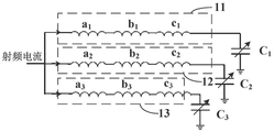
As shown in fig. 7, 8 and 9, fig. 7 is a schematic diagram illustrating a structure of an internal circuit of a plasma antenna coil provided in an embodiment of the present application; FIG. 8 illustrates a top view of a single inductor provided in an embodiment of the present application; fig. 9 shows an arrangement of a projection of the first portion (1) of the first inductor winding in the preset plane, a projection of the first portion (1) of the second inductor winding in the preset plane, and a projection of the first portion (1) of the third inductor winding in the preset plane, which are provided in an embodiment of the present application.
On the basis of any of the foregoing embodiments, in an embodiment of the present application, the at least 2 inductor coils 10 further include a third inductor coil 13, and a projection of a first portion (1) of the third inductor coil 13 in the preset plane overlaps with a projection of a second portion (2) of the first inductor coil 11 in the preset plane and a projection of a second portion of the second inductor coil 12 in the preset plane in the first direction R;
wherein the plasma inductance coil structure further comprises a third capacitor C electrically connected with the third inductance coil 133Said third capacitance C3The method is characterized in that the current of each inductance coil 10 is adjusted by adjusting the capacitance value of a capacitor electrically connected with each inductance coil 10 to adjust the size of a magnetic field generated by a first part of each inductance coil 10, so that the density distribution of plasmas in different areas of the surface of a wafer is adjusted by adjusting the size of the magnetic field in different areas of the surface of the wafer, and the etching rates at the same distance and different positions away from the center of the substrate are further adjusted, and the etching rates at the same distance and different positions away from the center of the substrate are more balanced.
It should be noted that, in the embodiments of the present application, the description is givenThird capacitor C3And the first capacitor C1And said second capacitance C2The capacitance value initially connected to the internal circuit of the inductor 10 may be the same or different, and optionally, in an embodiment of the present application, the third capacitor C3And the first capacitor C1And said second capacitance C2The capacitance value initially connected to the internal circuit of the inductor 10 is the same, and optionally, in one embodiment of the present application, the third capacitor C3The adjustment range of (95% d, 105% d), inclusive. The present application is not limited thereto, as the case may be.
It should be further noted that, in an embodiment of the present application, a size of the first inductor winding 11 in the first direction R, a size of the second inductor winding 12 in the first direction R, and a size of the third inductor winding 13 in the first direction R may all be the same, and in other embodiments of the present application, among the size of the first inductor winding 11 in the first direction R, the size of the second inductor winding 12 in the first direction R, and the size of the third inductor winding 13 in the first direction R, a size of at least one inductor winding 10 in the first direction R is different from a size of other inductor windings 10 in the first direction R, so as to prevent the inductor windings 10 from spatially affecting each other.
On the basis of any of the above embodiments, in an embodiment of the present application, as shown in fig. 9, a projection of the first portion (1) of the first inductor winding 11 in the preset plane, a projection of the first portion (1) of the second inductor winding 12 in the preset plane, and a projection of the first portion (1) of the third inductor winding 13 in the preset plane are connected end to form a closed loop, and a projection of the first portion (1) of the first inductor winding 11 in the preset plane, a projection of the first portion (1) of the second inductor winding 12 in the preset plane, and a projection of the first portion (1) of the third inductor winding 13 in the preset plane are uniformly distributed on the closed loop. Optionally, in an embodiment of the present application, a projection of the first portion (1) of the first inductor winding 11 in the preset plane, a projection of the first portion (1) of the second inductor winding 12 in the preset plane, and a projection of the first portion (1) of the third inductor winding 13 in the preset plane are connected end to form a closed circular ring, specifically, in an embodiment of the present application, a central angle corresponding to the first portion (1) of the first inductor winding 11 is 120 °, a central angle corresponding to the first portion (1) of the second inductor winding 12 is 120 °, a central angle corresponding to the first portion (1) of the third inductor winding 13 is 120 °, and the present application does not limit this, depending on the circumstances.
In other embodiments of the present application, a projection of the first portion (1) of the first inductor winding 11 in the preset plane, a projection of the first portion (1) of the second inductor winding 12 in the preset plane, and a projection of the first portion (1) of the third inductor winding 13 in the preset plane may not be located on the same closed loop, which is not limited in this application, as the case may be.
The projection of the first part (1) of the first inductor winding 11 in the preset plane, the projection of the first part (1) of the second inductor winding 12 in the preset plane, and the projection of the first part (1) of the third inductor winding 13 in the preset plane are connected end to form a closed ring, and the projection of the first part (1) of the first inductor winding 11 in the preset plane, the projection of the first part (1) of the second inductor winding 12 in the preset plane, and the projection of the first part (1) of the third inductor winding 13 in the preset plane are uniformly distributed on the closed ring.
On the basis of the above embodiments, in an embodiment of the present application, as shown in fig. 10, the magnetic field generated by the first portion (1) of the first inductor 11 corresponds to the etched area a1 of the substrate surface, the magnetic field generated by the first portion (1) of the second inductor 12 corresponds to the etched area B1 of the substrate surface, and the magnetic field generated by the first portion (1) of the third inductor 13 corresponds to the etched area C1 of the substrate surface, specifically, in an embodiment of the present application, if the etching unevenness occurs at different positions at the same distance from the center of the substrate in different etched areas, the capacitance value of the capacitor electrically connected with the first portion (1) of the inductor 10 corresponding to the etched area where the etched area is located is changed to change the magnitude of the radio frequency current of the first portion (1) of the inductor 10 corresponding to the etched area where the etched area is located, therefore, the etching rate of the etching area is adjusted, the etching uniformity of the surface of the substrate at the same distance from the center of the substrate at different positions is improved, and the phenomenon of uneven etching of the surface of the substrate at the same distance from the center of the substrate at different positions is improved.
It should be noted that, in the present application, when the capacitance of the inductor is adjusted, the density of the plasma changes more and more along the first direction R, and the etching rate changes more and more along the first direction R.
As shown in fig. 11, 12 and 13, fig. 11 is a schematic diagram showing a structure of an internal circuit of a plasma antenna coil provided in a further embodiment of the present application; FIG. 12 illustrates a top view of a single inductor provided in yet another embodiment of the present application; fig. 13 shows an arrangement of a projection of the first portion (1) of the first inductor winding in a preset plane, a projection of the first portion (1) of the second inductor winding in the preset plane, a projection of the first portion (1) of the third inductor winding in the preset plane, and a projection of the first portion (1) of the fourth inductor winding 14 in the preset plane, which are provided in another embodiment of the present application.
On the basis of any of the foregoing embodiments, in an embodiment of the present application, the at least 2 inductor coils 10 further include a fourth inductor coil 14, and a projection of a first portion (1) of the fourth inductor coil 14 in a preset plane overlaps with a projection of a second portion (2) of the first inductor coil 11 in the preset plane, a projection of a second portion (2) of the second inductor coil 12 in the preset plane, and a projection of a second portion (2) of the third inductor coil 13 in the preset plane in the first direction;
wherein, the plasma inductance coil structure also comprises a plasma inductance coil structureA fourth capacitor electrically connected to the fourth inductor 14, the fourth capacitor C4The method is characterized in that the current of each inductance coil 10 is adjusted by adjusting the capacitance value of a capacitor electrically connected with each inductance coil 10 to adjust the size of a magnetic field generated by a first part (1) of each inductance coil 10, so that the density distribution of plasmas in different etching areas on the surface of a wafer is adjusted by adjusting the size of the magnetic field in different areas on the surface of the wafer, and then the etching rates at the same distance and different positions away from the center of the substrate are adjusted, so that the etching rates at the same distance and different positions away from the center of the substrate are more balanced.
In other embodiments of the present application, the at least 2 inductor coils 10 further include more inductor coils 10, such as a fifth inductor coil, a sixth inductor coil, and so on, which is not limited in this application, as the case may be.
It should be noted that, in the embodiment of the present application, the fourth capacitor C4And the first capacitor C1The second capacitor C2And said three capacitors C3The capacitance value initially connected to the internal circuit of the inductor 10 may be the same or different, and preferably, in one embodiment of the present application, the fourth capacitor C4And the first capacitor C1The second capacitor C2And said third capacitance C3The capacitance value initially connected to the internal circuit of the inductor 10 is the same, and optionally, in one embodiment of the present application, the fourth capacitor C4The adjustment range of (95% d, 105% d), inclusive, is not limited in this application, as the case may be.
On the basis of the above-mentioned embodiments, in an embodiment of the present application, as shown in fig. 13, a projection of the first portion (1) of the first inductor winding 11 in the preset plane, a projection of the first portion (1) of the second inductor winding 12 in the preset plane, a projection of the first portion (1) of the third inductor winding 13 in the preset plane, and a projection of the first portion (1) of the fourth inductor winding 14 in the preset plane are connected end to form a closed loop, and a projection of the first portion (1) of the first inductor winding 11 in the preset plane, a projection of the first portion (1) of the second inductor winding 12 in the preset plane, a projection of the first portion (1) of the third inductor winding 13 in the preset plane, and a projection of the first portion (1) of the fourth inductor winding 14 in the preset plane are uniformly distributed on the closed loop .
On the basis of the above embodiment, in an embodiment of the present application, as shown in fig. 14, the magnetic field generated by the first portion (1) of the first inductor winding 11 corresponds to the etching region a2 of the substrate surface, the magnetic field generated by the first portion (1) of the second inductor winding 12 corresponds to the etching region B2 of the substrate surface, the magnetic field generated by the first portion (1) of the third inductor winding 13 corresponds to the etching region C2 of the substrate surface, and the magnetic field generated by the first portion (1) of the fourth inductor winding 14 corresponds to the etching region D2 of the substrate surface. It should be noted that, if the etching is not uniform in different etching regions of the substrate surface at the same distance from different positions of the center of the substrate, the magnitude of the radio frequency current of the first part (1) of the inductor coil 10 corresponding to the etching region where the etching region is located is changed by changing the capacitance value of the capacitor electrically connected to the first part (1) of the inductor coil 10 corresponding to different etching regions, so as to adjust the etching rate of the etching region, thereby improving the etching uniformity of the substrate surface at the same distance from the center of the substrate at different positions, and improving the etching non-uniformity of the substrate surface at the same distance from the center of the substrate at different positions.
In other embodiments of the present application, a projection of the first portion (1) of the first inductor winding 11 in the preset plane, a projection of the first portion (1) of the second inductor winding 12 in the preset plane, a projection of the first portion (1) of the third inductor winding 13 in the preset plane, and a projection of the first portion (1) of the fourth inductor winding 13 in the preset plane may not be located on the same closed ring, which is not limited in this application, depending on the circumstances.
Specifically, in an embodiment of the present application, as shown in fig. 15, a projection of the first portion (1) of the first inductor winding 11 and the first portion (1) of the second inductor winding 12 in a preset plane is located in an area surrounded by a projection of the first portion (1) of the third inductor winding 13 and the first portion (1) of the fourth inductor winding 14 in the preset plane.
On the basis of the above-mentioned embodiment, in an embodiment of the present application, as shown in fig. 15, a projection of the first portion (1) of the first inductor winding 11 in the preset plane and a projection of the first portion (1) of the second inductor winding 12 in the preset plane are symmetrical along an X axis, and a projection of the first portion (1) of the third inductor winding 13 in the preset plane and a projection of the first portion (1) of the fourth inductor winding 14 in the preset plane are symmetrical along a Y axis, wherein the X axis is perpendicular to the Y axis. Optionally, in an embodiment of the present application, a projection of the first portion (1) of the first inductor winding 11 in the preset plane and a projection of the first portion (1) of the second inductor winding 12 in the preset plane are connected end to form a closed circular ring M, a projection of the first portion (1) of the third inductor winding 13 in the preset plane and a projection of the first portion (1) of the fourth inductor winding 14 in the preset plane are connected end to form a closed circular ring N, and the circular ring M and the circular ring N share a circle center.
It should be noted that, when the inductance coils 10 are installed, on the premise of ensuring that the inductance coils 10 are not in contact with each other in space, the smaller the distance between the circular ring M formed by connecting the first part (1) of the first inductance coil 11 and the first part (1) of the second inductance coil 12 end to end in a projection on a preset plane, and the circular ring N formed by connecting the first part (1) of the third inductance coil 13 and the first part (1) of the fourth inductance coil 14 end to end in a projection on the preset plane, the better the distance between the circular rings is.
On the basis of any of the above embodiments, in an embodiment of the present application, a central angle corresponding to the first portion (1) of the first inductor winding 11 is 90 °, a central angle corresponding to the first portion (1) of the second inductor winding 12 is 90 °, a central angle corresponding to the first portion (1) of the third inductor winding 13 is 90 °, and a central angle corresponding to the first portion (1) of the fourth inductor winding 14 is 90 °, which is not limited in the present application, depending on the circumstances.
On the basis of the above embodiment, in an embodiment of the present application, as shown in fig. 16, the magnetic field generated by the first portion (1) of the first inductor winding 11 corresponds to the etching region X1 of the substrate surface, the magnetic field generated by the first portion (1) of the second inductor winding 12 corresponds to the etching region X2 of the substrate surface, the magnetic field generated by the first portion (1) of the third inductor winding 13 corresponds to the etching region Y1 of the substrate surface, and the magnetic field generated by the first portion (1) of the fourth inductor winding 14 corresponds to the etching region Y2 of the substrate surface. Specifically, in an embodiment of the present application, if the etching is not uniform in different etching regions at different positions at the same distance from the center of the substrate, the magnitude of the radio frequency current of the first portion (1) of the inductor 10 corresponding to the etching region where the etching region is located is changed by changing the capacitance value of the capacitor electrically connected to the first portion (1) of the inductor 10 corresponding to the different etching regions, so as to adjust the etching rate of the etching region, thereby improving the etching uniformity of the substrate surface at the same distance from the center thereof at different positions, and improving the non-uniform etching phenomenon of the substrate surface at the same distance from the center thereof at different positions.
On the basis of any of the above embodiments, in an embodiment of the present application, as shown in fig. 17, the second portion (2) of the inductor 10 includes a third sub-portion b and a fourth sub-portion d, and the first portion (1) further includes a fifth sub-portion e, and a projection of the fifth sub-portion e of the inductor 10 in the preset plane at least partially overlaps with a projection of the first sub-portion a of the inductor 10 in the preset plane or with a projection of the second sub-portion c of the inductor 10 in the preset plane in the first direction R, so that the magnetic field generated by the first portion (1) of the inductor 10 is relatively large, and thus the adjustment of the magnetic field generated by the first portion (1) of the inductor 10 can be achieved by adjusting a relatively small capacitance value.
Specifically, in an embodiment of the present application, the specific electrical connection structure of the first portion (1) and the second portion (2) of the inductor 10 is as follows: the input end of the first sub-part a is used for inputting radio frequency current, the output end of the first sub-part a of the inductance coil 10 is electrically connected with the input end of the third sub-part b, the output end of the third sub-part b is electrically connected with the input end of the second sub-part c, the output end of the second sub-part c is electrically connected with the input end of the fourth sub-part d, and the output end of the fourth sub-part d is electrically connected with the input end of the fifth sub-part e.
Optionally, in an embodiment of the present application, a projection of the first sub-portion a of the inductor 10 in a preset plane is located in a projection of the fifth sub-portion e of the inductor 10 in the preset plane; in another embodiment of the present application, a projection of the second sub-portion c of the inductor 10 in a predetermined plane is located in a projection of the fifth sub-portion e of the inductor 10 in the predetermined plane; in other embodiments of the present application, a projection of the first sub-portion a of the inductor 10 in the predetermined plane and a projection of the second sub-portion c of the inductor 10 in the predetermined plane are both located in a projection of the fifth sub-portion e of the inductor 10 in the predetermined plane, which is not limited in this application, as the case may be.
It should be noted that, in the embodiment of the present application, if the first portion (1) of the inductance coil 10 further includes a fifth sub-portion e, and the second portion (2) of the inductance coil 10 includes a third sub-portion b and a fourth sub-portion d, the output end of the fifth sub-portion e of the inductance coil 10 serves as the output end of the inductance coil 10.
It should be further noted that, in one embodiment of the present application, all the sub-portions of the inductance coil 10 are located on the same plane, and in order to save the occupied area of the projection of the plasma inductance coil structure in the preset plane in the first direction R, all the sub-portions of the inductance coil 10 are not located on the same plane, specifically, in one embodiment of the present application, all the sub-portions of the inductance coil 10 are not located on the same plane, in another embodiment of the present application, the first portion (1) and the second portion (2) of the inductance coil 10 are not located on the same plane, and all the sub-portions of the first portion (1) of the inductance coil 10 are located on the same plane, in other embodiments of the present application, the first portion (1) and the second portion (2) of the inductance coil 10 are not located on the same plane, and all the sub-portions of the second portion (2) of the inductance coil 10 are located on the same plane, the present application is not limited thereto, as the case may be.
The first portion (1) and the second portion (2) of the inductor (10) are not located on the same plane.
On the basis of the above embodiments, in one embodiment of the present application, the first portion (1) of each of the inductors 10 is located on the same side of the second portion (2) of each of the inductors 10.
On the basis of any of the above embodiments, in one embodiment of the present application, the voltage of the second portion (2) of the inductor 10 is smaller than the voltage of the first portion (1) of the inductor 10, and the second portions (2) of the at least 2 inductors 10 together form an electric field shielding ring, and the first portion (1) of the inductor 10 is located above the electric field shielding ring, it should be noted that, in the embodiment of the present application, the subsequent plasma inductor structure needs to be installed on the side of the gas shower head away from the reaction chamber of the plasma processing apparatus, wherein the second portion (2) of the inductor 10 is close to the side of the gas shower head away from the reaction chamber, and the first portion (1) of the inductor 10 is located on the side of the second portion (2) of the inductor 10 away from the gas shower head, so that the first portion (1) of the inductor 10 having a high voltage is distanced from the reaction chamber, thereby reducing the influence of the first portion (1) of the inductor 10 on the density distribution of the plasma in the reaction chamber.
It should be noted that if the voltage of the second portion (2) of the inductor 10 is lower than the voltage of the first portion (1) of the inductor 10, a standing wave needs to be formed in the inductor 10, and the standing wave is formed in the inductor 10 by: the input end and the output end of the inductance coil 10 are respectively and electrically connected with a capacitor, wherein one end of the capacitor close to the input end of the inductance coil 10 is electrically connected with the input end of the inductance coil 10, and the other end of the capacitor is used for inputting the radio frequency current.
In addition, in the embodiment of the present application, a capacitor electrically connected to the input end of the inductance coil 10 may be used as a part of the source rf circuit, which is not limited in the present application, as the case may be.
Based on this, on the basis of the above embodiment, in an embodiment of the present application, if the voltage of the second portion (2) of the inductor 10 is smaller than the voltage of the first portion (1) of the inductor 10, and the at least 2 inductors include the first inductor 11 and the second inductor 12, the plasma inductor structure further includes a fifth capacitor and a sixth capacitor, and the fifth capacitor is away from the first capacitor C from the first inductor 111Is electrically connected to the sixth capacitor, and the sixth capacitor is away from the second inductor 122Is electrically connected at one end. It should be noted that the fifth capacitor is a variable capacitor or a fixed capacitor, and the sixth capacitor is a variable capacitor or a fixed capacitor. Specifically, in an embodiment of the present application, the fifth capacitor and the sixth capacitor are both variable capacitors, in another embodiment of the present application, the fifth capacitor and the sixth capacitor are both fixed capacitors, and in other embodiments of the present application, one of the fifth capacitor and the sixth capacitor is a fixed capacitor and one of the fifth capacitor and the sixth capacitor is a variable capacitor, which is not limited in this application, and is determined as the case may be.
Specifically, in an embodiment of the present application, if the input end of the first inductor 11 is connected to the first capacitor C1Is electrically connected to the first capacitor C1The other end of the first inductor 12 is used for inputting radio frequency current, and the input end of the second inductor and the second capacitor C are connected2Is electrically connected to the second capacitor C2Is used for inputting radio frequency current, the output end of the first inductance coil 11 is electrically connected with one end of the fifth capacitor, soThe other end of the fifth capacitor is grounded, the output end of the second inductance coil 12 is electrically connected with one end of the sixth capacitor, and the other end of the sixth capacitor is grounded.
In another embodiment of the present application, if the output terminal of the first inductor 11 is connected to the first capacitor C1Is electrically connected to the first capacitor C1Is grounded, the output end of the second inductance coil 12 and the second capacitor C2Is electrically connected to the second capacitor C2The other end of the first inductor winding 11 is grounded, the input end of the first inductor winding is electrically connected to one end of the fifth capacitor, the other end of the fifth capacitor is used for inputting radio frequency current, the input end of the second inductor winding 12 is electrically connected to one end of the sixth capacitor, and the other end of the sixth capacitor is grounded.
On the basis of any of the above embodiments, in an embodiment of the present application, if the voltage of the second portion (2) of the inductor 10 is smaller than the voltage of the first portion (1) of the inductor 10, and the at least 2 inductors further include a third inductor 13, the plasma inductor structure further includes a seventh capacitor, and the seventh capacitor and the third inductor 13 deviate from the third capacitor C3Is electrically connected at one end. The seventh capacitor is a variable capacitor or a fixed capacitor.
Specifically, in an embodiment of the present application, if the input end of the third inductor 13 is connected to the third capacitor C3Is electrically connected to the third capacitor C3The other end of the third inductor winding 13 is used for inputting radio frequency current, the output end of the third inductor winding is electrically connected with one end of the seventh capacitor, and the other end of the seventh capacitor is grounded. In another embodiment of the present application, if the output terminal of the third inductor winding 13 is connected to the third capacitor C3Is electrically connected to the third capacitor C3The other end of the third inductor 13 is grounded, the input end of the third inductor is electrically connected to one end of the seventh capacitor, and the other end of the seventh capacitor is used for inputting radio frequency current.
On the basis of any of the above embodiments, in an embodiment of the present application, if the voltage of the second portion (2) of the inductor 10 is smaller than the voltage of the first portion (1) of the inductor 10, and the at least 2 inductors further include a fourth inductor 14, the plasma inductor structure further includes an eighth capacitor, and the eighth capacitor and the fourth inductor 14 deviate from the fourth capacitor C4Is electrically connected at one end. The eighth capacitor is a variable capacitor or a fixed capacitor.
Specifically, in an embodiment of the present application, if the input end of the fourth inductor 14 is connected to the fourth capacitor C4Is electrically connected to the fourth capacitor C4The other end of the fourth inductor winding 14 is used for inputting radio frequency current, the output end of the fourth inductor winding is electrically connected with one end of the eighth capacitor, and the other end of the eighth capacitor is grounded. In another embodiment of the present application, if the output terminal of the fourth inductor 14 is connected to the fourth capacitor C4Is electrically connected to the fourth capacitor C4The other end of the fourth inductor 14 is grounded, the input end of the fourth inductor is electrically connected to one end of the eighth capacitor, and the other end of the eighth capacitor is used for inputting radio frequency current.
Accordingly, as shown in fig. 18, the present application also provides a plasma processing apparatus comprising:
a reaction chamber 1;
the gas spray header 2 is positioned in the reaction cavity 1;
the plasma inductance coil structure 3 is positioned on one side of the gas spray header 2, which is far away from the reaction cavity 1, and the plasma inductance coil structure 3 is the plasma inductance coil structure 3 provided by any one of the embodiments;
and the base station 4 is positioned on one side of the gas spray head 2 departing from the plasma induction coil structure 3 and is used for placing a substrate.
In the plasma processing equipment provided by the embodiment of the application, when the plasma processing equipment is applied to etching, the plasma processing equipment can be used for processing the etching condition and the etching requirement based on the surface of the substrateBy varying said first capacitance C4And said second capacitance C4Of the first capacitor C, changing the capacitance value of at least one of the capacitors C4And said second capacitance C4The ratio of the first inductance coil 11 to the second inductance coil 12 to the first inductance coil 11, so that the magnetic field generated by the first part (1) of the first inductance coil and/or the magnetic field generated by the first part (1) of the second inductance coil 12 can be adjusted to adjust the density distribution of plasmas in different areas on the surface of the wafer, and the etching rates of the positions at the same distance and different positions from the center of the substrate can be adjusted, so that the etching rates of the position at the same distance and different positions from the center of the substrate are more balanced, the etching uniformity of the position at the same distance and different positions from the center of the substrate is improved, and the phenomenon of uneven etching of the position at the same distance and different positions from.
Accordingly, as shown in fig. 19, the present application also provides a plasma processing method applied to the plasma processing apparatus provided in any one of the above embodiments, the plasma processing method including:
placing the substrate on a stage 4;
performing plasma treatment on a first surface of the substrate;
adjusting the first capacitance C based on the etching rate of different areas of the substrate1And said second capacitance C2Of at least one capacitor, changing said first capacitance C1And said second capacitance C2To adjust an etch rate of the first surface of the substrate.
In the plasma processing method provided by the embodiment of the application, when the plasma processing method is applied to etching, the plasma processing method can change the first capacitor C based on the etching requirement and the etching condition of the surface of the substrate1And said second capacitance C2Of the first capacitor C, changing the capacitance value of at least one of the capacitors C1And said second capacitance C2So as to adjust the magnitude of the magnetic field generated by the first portion (1) of the first inductor winding 11 and/or the magnetic field generated by the first portion (1) of the second inductor winding 12, thereby adjusting the waferThe density distribution of plasmas in different areas on the surface is adjusted, so that the etching rates of the positions, which are away from the center of the substrate, at the same distance and different positions are adjusted, the etching rates of the positions, which are away from the center of the substrate, at the same distance and different positions are balanced, the etching uniformity of the positions, which are away from the center of the substrate, at the same distance and different positions is improved, and the phenomenon of uneven etching of the positions, which are away from the center of the substrate, at the same distance and.
It should be noted that if the capacitance value of the capacitor electrically connected to the inductor is larger, the rf current of the first portion (1) of the inductor 10 is larger, so that the magnetic field strength generated by the first portion (1) of the inductor 10 is larger, so that the etching rate of the etched area of the surface of the substrate corresponding to the first portion (1) of the inductor 10 is larger, whereas if the capacitance value of the capacitor electrically connected to the inductor is smaller, the rf current of the first portion (1) of the inductor 10 is smaller, so that the magnetic field strength generated by the first portion (1) of the inductor 10 is smaller, so that the etching rate of the etched area of the surface of the substrate corresponding to the first portion (1) of the inductor 10 is smaller.
It should be further noted that, if there is a position in one etching region that is at the same distance from the center of the substrate and a position in another etching region that is at the same distance from the center of the substrate, the etching degree is different, in an embodiment of the present application, the plasma processing method includes: by varying the first capacitance C1And a second capacitor C2To adjust an etch rate of the surface of the substrate.
On the basis of the foregoing embodiment, in an embodiment of the present application, if the at least 2 inductor coils further include a third inductor coil, and a position in one etching region at the same distance from the center of the substrate is different in etching degree from a position in other etching regions at the same distance from the center of the substrate, in an embodiment of the present application, the plasma processing method includes: by varying the first capacitance C1A second capacitor C2A third capacitor C3To adjust an etch rate of the surface of the substrate.
On the basis of the above embodiment, in an embodiment of the present application, if there are two etching regions having different etching degrees at positions that are at the same distance from the center of the substrate, in an embodiment of the present application, the plasma processing method includes: by varying the first capacitance C1A second capacitor C2A third capacitor C3To adjust an etch rate of the surface of the substrate.
On the basis of the above embodiment, in an embodiment of the present application, if the etching degrees of the positions away from the center of the substrate in the three etching regions are different, the plasma processing method includes: by varying the first capacitance C1A second capacitor C2A third capacitor C3To adjust an etch rate of the surface of the substrate.
On the basis of the foregoing embodiment, in an embodiment of the present application, if the at least 2 inductor coils further include a fourth inductor coil, and a position in one etching region at the same distance from the center of the substrate is different in etching degree from a position in other etching regions at the same distance from the center of the substrate, in an embodiment of the present application, the plasma processing method includes: by varying the first capacitance C1A second capacitor C2A third capacitor C3And a fourth capacitance C4To adjust an etch rate of the surface of the substrate.
On the basis of the above embodiment, in an embodiment of the present application, if there are two etching regions having different etching degrees at positions that are at the same distance from the center of the substrate, in an embodiment of the present application, the plasma processing method includes: by varying the first capacitance C1A second capacitor C2A third capacitor C3And a fourth capacitance C4To adjust the surface of the substrateThe etch rate of the facet.
On the basis of the above embodiment, in an embodiment of the present application, if the etching degree of the positions away from the center of the substrate in the three etching regions is different, the plasma processing method includes: by varying the first capacitance C1A second capacitor C2A third capacitor C3And a fourth capacitance C4To adjust an etch rate of the surface of the substrate.
On the basis of the above embodiment, in an embodiment of the present application, if the etching degrees of the positions away from the center of the substrate in the four etching regions are different, the plasma processing method includes: by varying the first capacitance C1A second capacitor C2A third capacitor C3And a fourth capacitance C4To adjust an etch rate of the surface of the substrate.
The plasma inductance coil structure, the plasma processing device and the processing method provided by the embodiment of the application, the magnetic field intensity generated by the first part (1) a of the inductance coil 10 is larger than the magnetic field intensity generated by the second part (2) c of the inductance coil 10, so that the inductance coil 10 forms an asymmetric magnetic field, and the projection of the first part (1) of the first inductance coil 11 and the projection of the second part (2) of the second inductance coil 12 in the preset plane included in the at least 2 inductance coils 10 are at least partially overlapped on the first direction R to compensate the magnitude of the magnetic field intensity generated by the second part (2) of the second inductance coil 12, and simultaneously the projection of the second part (2) of the first inductance coil 11 in the preset plane and the projection of the first part (1) of the second inductance coil 12 in the preset plane are at least partially heavy on the first direction R Is stacked to compensate for the magnitude of the magnetic field intensity generated by the second part (2) of the first inductor winding 11, due to the first capacitor C electrically connected to the first inductor winding 111And a second capacitor C electrically connected to the second inductor 122In which at least one of the capacitors is an adjustable capacitor, fromWhile the magnitude of the magnetic field generated by the first part (1) of the first inductor winding 11 and/or the magnetic field generated by the first part (1) of the second inductor winding 12 can be adjusted.
Therefore, when the capacitor is applied to etching, based on the etching requirement and the etching condition of the surface of the substrate, the first capacitor C can be changed1And said second capacitance C2Thereby changing the first capacitance C1And said second capacitance C2The ratio of the first inductance coil 11 to the second inductance coil 12 to the first portion (1) of the magnetic field generated by the first portion (1) of the magnetic field and/or the second inductance coil 12 to adjust the etching rate of the substrate surface to the center of the substrate at the same distance and different positions, so that the etching rate of the substrate surface to the center of the substrate at the same distance and different positions is balanced, the etching uniformity of the substrate surface to the center of the substrate at the same distance and different positions is improved, and the phenomenon of uneven etching of the substrate surface to the center of the substrate at the same distance and different positions is improved.
Moreover, the plasma inductance coil structure provided by the application only needs to change the first capacitor C1And said second capacitance C2Of at least one capacitor, changing said first capacitance C1And said second capacitance C2The ratio of, and need not can adjust the distance through the levelness of adjusting plasma inductance coils structure the same etching rate of different positions department of distance of pending wafer center for the inclination that can not introduce plasma inductance coils structure in this application is difficult for a lot of complicated technical problem such as control, thereby makes when using the plasma inductance coils structure that this application provided, the adjusting distance that can be simple and convenient the same etching rate of different positions department of distance of wafer center.
In addition, the present application is directed to the method of forming a capacitor by varying the first capacitance C1And said second capacitance C2To change the first capacitance C1And said second capacitance C2To adjust the ratio of (a) to (b) to (c) to (d) to (The magnetic field and/or the magnetic field generated by the first part (1) of the second inductance coil 12 are/is adjusted, so that the density distribution of plasmas in different areas of the surface of the wafer is adjusted by adjusting the size of the magnetic field in different areas of the surface of the wafer, the etching rate of the plasma inductance coil structure at the same distance and different positions away from the center of the wafer is adjusted, and the phenomenon of nonuniform transverse etching is improved. Therefore, the variation range of the ratio of the capacitance can be very small in the application, so that fine magnetic field adjustment can be realized, the plasma inductance coil structure generates an uneven magnetic field by adjusting the levelness of the plasma inductance coil structure, and the horizontal etching rate of an etching area is adjusted.
All parts in the specification are described in a parallel and progressive mode, each part is mainly described to be different from other parts, and the same and similar parts among all parts can be referred to each other.
The previous description of the disclosed embodiments is provided to enable any person skilled in the art to make or use the present application. Various modifications to these embodiments will be readily apparent to those skilled in the art, and the generic principles defined herein may be applied to other embodiments without departing from the spirit or scope of the application. Thus, the present application is not intended to be limited to the embodiments shown herein but is to be accorded the widest scope consistent with the principles and novel features disclosed herein.
Claims (16)
1. A plasma inductor structure, comprising:
at least 2 inductive coils, each said inductive coil comprising a first portion and a second portion, wherein said first portion generates a magnetic field strength greater than a magnetic field strength generated by said second portion;
the at least 2 inductor coils comprise: the first inductance coil and the second inductance coil are arranged, wherein the projection of the first part of the first inductance coil in a preset plane is at least partially overlapped with the projection of the second part of the second inductance coil in the preset plane in the first direction;
the first capacitor is electrically connected with the first inductance coil, the second capacitor is electrically connected with the second inductance coil, and at least one of the first capacitor and the second capacitor is an adjustable capacitor;
the preset plane is a plane where the wafer is located when the wafer is subjected to plasma processing by the inductance coil, and the first direction is the radial direction of the inductance coil.
2. The plasma inductor structure of claim 1, wherein the output of the first inductor is electrically connected to the first capacitor and the output of the second inductor is electrically connected to the second capacitor.
3. The plasma inductor structure of claim 2, wherein the first capacitor is an adjustable capacitor and the second capacitor is a fixed capacitor.
4. The plasma inductor structure of claim 2, wherein the first capacitance is an adjustable capacitance and the second capacitance is an adjustable capacitance.
5. The plasma inductor structure of claim 1, wherein a projection of the first portion of the first inductor winding in the predetermined plane completely overlaps a projection of the second portion of the second inductor winding in the first direction in the predetermined plane.
6. The plasma inductor structure of claim 1, wherein the first portion of the inductor coil comprises a first sub-portion and a second sub-portion, a projection of the first sub-portion in the predetermined plane and a projection of the second sub-portion in the predetermined plane at least partially overlap in the first direction.
7. The plasma inductor structure of claim 6, wherein the second portion of the inductor coil further comprises a third subsection and a fourth subsection, and the first portion of the inductor coil further comprises a fifth subsection, a projection of the fifth subsection of the inductor coil in the predetermined plane at least partially overlapping with the projection of the first subsection of the inductor coil in the predetermined plane or with the projection of the second subsection of the inductor coil in the predetermined plane in the first direction.
8. The plasma inductor structure of claim 1, wherein the at least 2 inductors further comprise a third inductor, a projection of a first portion of the third inductor in the predetermined plane overlapping in the first direction with a projection of a second portion of the first inductor in the predetermined plane and a projection of a second portion of the second inductor in the predetermined plane;
the plasma inductance coil structure further comprises a third capacitor electrically connected with the third inductance coil, and the third capacitor is an adjustable capacitor.
9. The plasma inductor structure of claim 8, wherein a projection of the first portion of the first inductor winding in the predetermined plane, a projection of the first portion of the second inductor winding in the predetermined plane, and a projection of the first portion of the third inductor winding in the predetermined plane are connected end to form a closed loop, and a projection of the first portion of the first inductor winding in the predetermined plane, a projection of the first portion of the second inductor winding in the predetermined plane, and a projection of the first portion of the third inductor winding in the predetermined plane are uniformly distributed on the closed loop.
10. The plasma inductor structure of claim 8, wherein the at least 2 inductors further comprise a fourth inductor, a projection of a first portion of the fourth inductor in the predetermined plane overlapping a projection of a second portion of the first inductor in the predetermined plane, a projection of a second portion of the second inductor in the predetermined plane, and a projection of a second portion of the third inductor in the predetermined plane in the first direction;
the plasma inductance coil structure further comprises a fourth capacitor electrically connected with the fourth inductance coil, and the fourth capacitor is an adjustable capacitor.
11. The plasma inductor structure of claim 10, wherein a projection of the first portion of the first inductor winding in the predetermined plane, a projection of the first portion of the second inductor winding in the predetermined plane, a projection of the first portion of the third inductor winding in the predetermined plane, and a projection of the first portion of the fourth inductor winding in the predetermined plane are connected end-to-end to form a closed loop, and wherein a projection of the first portion of the first inductor winding in the predetermined plane, a projection of the first portion of the second inductor winding in the predetermined plane, and a projection of the first portion of the third inductor winding in the predetermined plane and a projection of the first portion of the fourth inductor winding in the predetermined plane are uniformly distributed on the closed loop.
12. The plasma inductor structure of claim 10, wherein a projection of the first portion of the first inductor winding in the predetermined plane and a projection of the first portion of the second inductor winding in the predetermined plane are located in an area surrounded by a projection of the first portion of the third inductor winding and a projection of the first portion of the fourth inductor winding in the predetermined plane, and wherein a projection of the first portion of the first inductor winding in the predetermined plane and a projection of the first portion of the second inductor winding in the predetermined plane are symmetric along an X-axis, and a projection of the first portion of the third inductor winding in the predetermined plane and a projection of the first portion of the fourth inductor winding in the predetermined plane are symmetric along a Y-axis, wherein the X-axis is perpendicular to the Y-axis.
13. The plasma inductor structure of claim 1, wherein the voltage of the second portion of the inductor is less than the voltage of the first portion of the inductor, the second portions of the at least 2 inductors together forming an electric field shield ring, the first portion of the inductor being positioned above the electric field shield ring.
14. The plasma inductor structure of claim 13, further comprising a fifth capacitor electrically connected to an end of the first inductor facing away from the first capacitor, and a sixth capacitor electrically connected to an end of the second inductor facing away from the second capacitor.
15. A plasma processing apparatus, comprising:
a reaction chamber;
the gas spray header is positioned in the reaction cavity;
a plasma inductor structure located on a side of the gas showerhead facing away from the reaction chamber, the plasma inductor structure being as defined in any one of claims 1 to 14;
and the base station is positioned on one side of the gas spray head, which deviates from the plasma inductance coil structure, and is used for placing a substrate.
16. A plasma processing method applied to the plasma processing apparatus according to claim 15, comprising:
placing a substrate on a submount;
performing plasma treatment on a first surface of the substrate;
and adjusting the capacitance value of at least one of the first capacitor and the second capacitor based on the etching rate of different areas of the substrate, and changing the ratio of the first capacitor to the second capacitor so as to adjust the etching rate of the first surface of the substrate.
Priority Applications (2)
| Application Number | Priority Date | Filing Date | Title |
|---|---|---|---|
| CN201911424310.5A CN113133175B (en) | 2019-12-31 | 2019-12-31 | Plasma inductance coil structure, plasma processing equipment and processing method |
| TW109140502A TWI790500B (en) | 2019-12-31 | 2020-11-19 | Plasma induction coil structure, plasma processing equipment and processing method |
Applications Claiming Priority (1)
| Application Number | Priority Date | Filing Date | Title |
|---|---|---|---|
| CN201911424310.5A CN113133175B (en) | 2019-12-31 | 2019-12-31 | Plasma inductance coil structure, plasma processing equipment and processing method |
Publications (2)
| Publication Number | Publication Date |
|---|---|
| CN113133175A true CN113133175A (en) | 2021-07-16 |
| CN113133175B CN113133175B (en) | 2024-02-09 |
Family
ID=76769825
Family Applications (1)
| Application Number | Title | Priority Date | Filing Date |
|---|---|---|---|
| CN201911424310.5A Active CN113133175B (en) | 2019-12-31 | 2019-12-31 | Plasma inductance coil structure, plasma processing equipment and processing method |
Country Status (2)
| Country | Link |
|---|---|
| CN (1) | CN113133175B (en) |
| TW (1) | TWI790500B (en) |
Cited By (2)
| Publication number | Priority date | Publication date | Assignee | Title |
|---|---|---|---|---|
| US20230162986A1 (en) * | 2021-11-24 | 2023-05-25 | Shanghai Huali Integrated Circuit Corporation | Method for Improving Plasma Distribution in Etching |
| WO2024140536A1 (en) * | 2022-12-30 | 2024-07-04 | 江苏鲁汶仪器股份有限公司 | Ion beam etching uniformity adjustment apparatus and method |
Citations (20)
| Publication number | Priority date | Publication date | Assignee | Title |
|---|---|---|---|---|
| JPH0681152A (en) * | 1991-03-20 | 1994-03-22 | Ulvac Japan Ltd | Plasma treating device |
| JPH09161993A (en) * | 1995-12-12 | 1997-06-20 | Hitachi Ltd | Plasma processing apparatus and method having multi-stage coil using double coil |
| US5880034A (en) * | 1997-04-29 | 1999-03-09 | Princeton University | Reduction of semiconductor structure damage during reactive ion etching |
| US20020033231A1 (en) * | 1998-02-26 | 2002-03-21 | Matsushita Electronics Corporation | Apparatus and method for plasma etching |
| DE10051831A1 (en) * | 1999-07-20 | 2002-05-02 | Bosch Gmbh Robert | Inductively-coupled plasma-etching equipment for silicon substrates includes two stacked coils producing field between substrate and ICP source |
| GB0306752D0 (en) * | 2000-10-19 | 2003-04-30 | Bosch Gmbh Robert | Device and method for etching a substrate by means of an inductively coupled plasma |
| CN1937880A (en) * | 2005-12-08 | 2007-03-28 | 北京北方微电子基地设备工艺研究中心有限责任公司 | Inductive coupling source |
| US20080178806A1 (en) * | 2004-10-13 | 2008-07-31 | Adaptive Plasma Technology Corp. | Plasma Source For Uniform Plasma Distribution in Plasma Chamber |
| CN101500369A (en) * | 2008-01-30 | 2009-08-05 | 北京北方微电子基地设备工艺研究中心有限责任公司 | Inductor coupling coil and inductor coupling plasma generation apparatus |
| CN101543141A (en) * | 2006-11-28 | 2009-09-23 | 莎姆克株式会社 | Plasma processing apparatus |
| CN201869430U (en) * | 2010-11-25 | 2011-06-15 | 中微半导体设备(上海)有限公司 | Radio frequency antenna used in plasma generator |
| KR20110006070U (en) * | 2011-04-05 | 2011-06-16 | 재단법인서울대학교산학협력재단 | Magnetized inductively coupled plasma processing apparatus |
| US20120298303A1 (en) * | 2010-11-30 | 2012-11-29 | Canon Anelva Corporation | Plasma treatment apparatus |
| CN102983051A (en) * | 2011-09-05 | 2013-03-20 | 中微半导体设备(上海)有限公司 | Plasma treatment device with adjustable plasma concentration distribution and processing method thereof |
| CN103168507A (en) * | 2010-10-28 | 2013-06-19 | 应用材料公司 | Plasma processing apparatus with reduced effects of process chamber asymmetry |
| CN103839742A (en) * | 2012-11-28 | 2014-06-04 | 中微半导体设备(上海)有限公司 | Magnetic field distribution regulation device and method for plasma processor |
| JP2016001609A (en) * | 2015-07-15 | 2016-01-07 | 東京エレクトロン株式会社 | Plasma processing equipment |
| CN105655223A (en) * | 2015-12-28 | 2016-06-08 | 上海集成电路研发中心有限公司 | Magnetic field generating device of plasma etching system |
| CN105719928A (en) * | 2014-12-03 | 2016-06-29 | 中微半导体设备(上海)有限公司 | Device and method for compensating non-uniformity of etching rate in ICP etching |
| CN107333378A (en) * | 2016-04-29 | 2017-11-07 | 中微半导体设备(上海)有限公司 | A kind of device for inductively coupled plasma processing and its control method |
Family Cites Families (1)
| Publication number | Priority date | Publication date | Assignee | Title |
|---|---|---|---|---|
| CN105470087B (en) * | 2014-09-11 | 2017-07-07 | 中微半导体设备(上海)有限公司 | A kind of inductance coupling plasma processing device |
-
2019
- 2019-12-31 CN CN201911424310.5A patent/CN113133175B/en active Active
-
2020
- 2020-11-19 TW TW109140502A patent/TWI790500B/en active
Patent Citations (22)
| Publication number | Priority date | Publication date | Assignee | Title |
|---|---|---|---|---|
| JPH0681152A (en) * | 1991-03-20 | 1994-03-22 | Ulvac Japan Ltd | Plasma treating device |
| JPH09161993A (en) * | 1995-12-12 | 1997-06-20 | Hitachi Ltd | Plasma processing apparatus and method having multi-stage coil using double coil |
| US5880034A (en) * | 1997-04-29 | 1999-03-09 | Princeton University | Reduction of semiconductor structure damage during reactive ion etching |
| US20020033231A1 (en) * | 1998-02-26 | 2002-03-21 | Matsushita Electronics Corporation | Apparatus and method for plasma etching |
| DE10051831A1 (en) * | 1999-07-20 | 2002-05-02 | Bosch Gmbh Robert | Inductively-coupled plasma-etching equipment for silicon substrates includes two stacked coils producing field between substrate and ICP source |
| GB0306752D0 (en) * | 2000-10-19 | 2003-04-30 | Bosch Gmbh Robert | Device and method for etching a substrate by means of an inductively coupled plasma |
| US20080178806A1 (en) * | 2004-10-13 | 2008-07-31 | Adaptive Plasma Technology Corp. | Plasma Source For Uniform Plasma Distribution in Plasma Chamber |
| CN1937880A (en) * | 2005-12-08 | 2007-03-28 | 北京北方微电子基地设备工艺研究中心有限责任公司 | Inductive coupling source |
| CN101543141A (en) * | 2006-11-28 | 2009-09-23 | 莎姆克株式会社 | Plasma processing apparatus |
| CN103347360A (en) * | 2006-11-28 | 2013-10-09 | 莎姆克株式会社 | Plasma processing apparatus |
| CN101500369A (en) * | 2008-01-30 | 2009-08-05 | 北京北方微电子基地设备工艺研究中心有限责任公司 | Inductor coupling coil and inductor coupling plasma generation apparatus |
| CN103168507A (en) * | 2010-10-28 | 2013-06-19 | 应用材料公司 | Plasma processing apparatus with reduced effects of process chamber asymmetry |
| CN201869430U (en) * | 2010-11-25 | 2011-06-15 | 中微半导体设备(上海)有限公司 | Radio frequency antenna used in plasma generator |
| US20120298303A1 (en) * | 2010-11-30 | 2012-11-29 | Canon Anelva Corporation | Plasma treatment apparatus |
| CN103081073A (en) * | 2010-11-30 | 2013-05-01 | 佳能安内华股份有限公司 | Plasma processing device |
| KR20110006070U (en) * | 2011-04-05 | 2011-06-16 | 재단법인서울대학교산학협력재단 | Magnetized inductively coupled plasma processing apparatus |
| CN102983051A (en) * | 2011-09-05 | 2013-03-20 | 中微半导体设备(上海)有限公司 | Plasma treatment device with adjustable plasma concentration distribution and processing method thereof |
| CN103839742A (en) * | 2012-11-28 | 2014-06-04 | 中微半导体设备(上海)有限公司 | Magnetic field distribution regulation device and method for plasma processor |
| CN105719928A (en) * | 2014-12-03 | 2016-06-29 | 中微半导体设备(上海)有限公司 | Device and method for compensating non-uniformity of etching rate in ICP etching |
| JP2016001609A (en) * | 2015-07-15 | 2016-01-07 | 東京エレクトロン株式会社 | Plasma processing equipment |
| CN105655223A (en) * | 2015-12-28 | 2016-06-08 | 上海集成电路研发中心有限公司 | Magnetic field generating device of plasma etching system |
| CN107333378A (en) * | 2016-04-29 | 2017-11-07 | 中微半导体设备(上海)有限公司 | A kind of device for inductively coupled plasma processing and its control method |
Non-Patent Citations (3)
| Title |
|---|
| J. GRUENWALD, 等: "Foundations of a laser-accelerated plasma diagnostics and beam stabilization with miniaturized Rogowski coils", NUCLEAR INSTRUMENTS AND METHODS IN PHYSICS RESEARCH SECTION A: ACCELERATORS, SPECTROMETERS, DETECTORS AND ASSOCIATED EQUIPMENT, vol. 883 * |
| 汪献伟;王兆亮;何庆;李秀莲;: "CFETR CSMC装配误差下的电磁状态研究", 低温物理学报, no. 06 * |
| 陈国雄;钱高荣;宣冬冬;苏翔;程瑜华;: "一种可产生均匀磁场的并联发射线圈结构", 杭州电子科技大学学报(自然科学版), no. 05 * |
Cited By (2)
| Publication number | Priority date | Publication date | Assignee | Title |
|---|---|---|---|---|
| US20230162986A1 (en) * | 2021-11-24 | 2023-05-25 | Shanghai Huali Integrated Circuit Corporation | Method for Improving Plasma Distribution in Etching |
| WO2024140536A1 (en) * | 2022-12-30 | 2024-07-04 | 江苏鲁汶仪器股份有限公司 | Ion beam etching uniformity adjustment apparatus and method |
Also Published As
| Publication number | Publication date |
|---|---|
| TW202127504A (en) | 2021-07-16 |
| TWI790500B (en) | 2023-01-21 |
| CN113133175B (en) | 2024-02-09 |
Similar Documents
| Publication | Publication Date | Title |
|---|---|---|
| US10020167B2 (en) | Plasma processing apparatus | |
| KR101870791B1 (en) | Plasma processing apparatus | |
| JP3903034B2 (en) | Inductively coupled plasma generator with serpentine coil antenna | |
| JP4646272B2 (en) | Plasma processing equipment | |
| US7285916B2 (en) | Multi chamber plasma process system | |
| US20020018025A1 (en) | Power supply antenna and power supply method | |
| JP2011103346A (en) | Plasma processing apparatus | |
| JP7416986B2 (en) | Coil structure and plasma processing equipment | |
| WO2003013198A1 (en) | Antenna structure for inductively coupled plasma generator | |
| US8956500B2 (en) | Methods to eliminate “M-shape” etch rate profile in inductively coupled plasma reactor | |
| TWI656559B (en) | Operation method for plasma treatment apparatus | |
| US20150097480A1 (en) | Plasma equipment | |
| SG182966A1 (en) | Arrays of inductive elements for minimizing radial non-uniformity in plasma | |
| US10115566B2 (en) | Method and apparatus for controlling a magnetic field in a plasma chamber | |
| KR20160123388A (en) | Controlling azimuthal uniformity of etch process in plasma processing chamber | |
| CN113133175B (en) | Plasma inductance coil structure, plasma processing equipment and processing method | |
| TWI553693B (en) | An inductance coil and inductively coupled plasma processing device | |
| US20230411117A1 (en) | Antenna member and apparatus and method for treating substrate | |
| US10892139B2 (en) | ICP antenna and substrate processing device including the same | |
| KR102419421B1 (en) | Antenna structure for generating inductively coupled plasma | |
| KR102081686B1 (en) | Substrate processing method using plasma | |
| CN113838734A (en) | Plasma processing apparatus and substrate processing method | |
| JP2014075362A (en) | Plasma processing device | |
| KR20050059858A (en) | Power supply system comprising a plurality of electrode blocks | |
| TW202244978A (en) | Induction coil assembly for plasma processing apparatus |
Legal Events
| Date | Code | Title | Description |
|---|---|---|---|
| PB01 | Publication | ||
| PB01 | Publication | ||
| SE01 | Entry into force of request for substantive examination | ||
| SE01 | Entry into force of request for substantive examination | ||
| GR01 | Patent grant | ||
| GR01 | Patent grant |