[go: up one dir, main page]

CN112928825A - Method for determining quality factor and wireless charger - Google Patents

Method for determining quality factor and wireless charger Download PDF

Info

Publication number
CN112928825A
CN112928825A CN201911254542.0A CN201911254542A CN112928825A CN 112928825 A CN112928825 A CN 112928825A CN 201911254542 A CN201911254542 A CN 201911254542A CN 112928825 A CN112928825 A CN 112928825A
Authority
CN
China
Prior art keywords
switch
inverter
filter
capacitor
wireless charger
Prior art date
Legal status (The legal status is an assumption and is not a legal conclusion. Google has not performed a legal analysis and makes no representation as to the accuracy of the status listed.)
Pending
Application number
CN201911254542.0A
Other languages
Chinese (zh)
Inventor
王德昌
江登宇
盛儒洋
毛欢
Current Assignee (The listed assignees may be inaccurate. Google has not performed a legal analysis and makes no representation or warranty as to the accuracy of the list.)
NXP USA Inc
Original Assignee
NXP USA Inc
Priority date (The priority date is an assumption and is not a legal conclusion. Google has not performed a legal analysis and makes no representation as to the accuracy of the date listed.)
Filing date
Publication date
Application filed by NXP USA Inc filed Critical NXP USA Inc
Priority to CN201911254542.0A priority Critical patent/CN112928825A/en
Priority to US17/104,163 priority patent/US11990781B2/en
Publication of CN112928825A publication Critical patent/CN112928825A/en
Pending legal-status Critical Current

Links

Images

Classifications

    • GPHYSICS
    • G01MEASURING; TESTING
    • G01RMEASURING ELECTRIC VARIABLES; MEASURING MAGNETIC VARIABLES
    • G01R27/00Arrangements for measuring resistance, reactance, impedance, or electric characteristics derived therefrom
    • G01R27/02Measuring real or complex resistance, reactance, impedance, or other two-pole characteristics derived therefrom, e.g. time constant
    • G01R27/26Measuring inductance or capacitance; Measuring quality factor, e.g. by using the resonance method; Measuring loss factor; Measuring dielectric constants ; Measuring impedance or related variables
    • G01R27/2688Measuring quality factor or dielectric loss, e.g. loss angle, or power factor
    • H02J7/80
    • HELECTRICITY
    • H02GENERATION; CONVERSION OR DISTRIBUTION OF ELECTRIC POWER
    • H02JCIRCUIT ARRANGEMENTS OR SYSTEMS FOR SUPPLYING OR DISTRIBUTING ELECTRIC POWER; SYSTEMS FOR STORING ELECTRIC ENERGY
    • H02J50/00Circuit arrangements or systems for wireless supply or distribution of electric power
    • H02J50/10Circuit arrangements or systems for wireless supply or distribution of electric power using inductive coupling
    • H02J50/12Circuit arrangements or systems for wireless supply or distribution of electric power using inductive coupling of the resonant type
    • HELECTRICITY
    • H02GENERATION; CONVERSION OR DISTRIBUTION OF ELECTRIC POWER
    • H02JCIRCUIT ARRANGEMENTS OR SYSTEMS FOR SUPPLYING OR DISTRIBUTING ELECTRIC POWER; SYSTEMS FOR STORING ELECTRIC ENERGY
    • H02J7/00Circuit arrangements for charging or depolarising batteries or for supplying loads from batteries
    • H02J7/02Circuit arrangements for charging or depolarising batteries or for supplying loads from batteries for charging batteries from AC mains by converters
    • H02J7/04Regulation of charging current or voltage
    • HELECTRICITY
    • H02GENERATION; CONVERSION OR DISTRIBUTION OF ELECTRIC POWER
    • H02JCIRCUIT ARRANGEMENTS OR SYSTEMS FOR SUPPLYING OR DISTRIBUTING ELECTRIC POWER; SYSTEMS FOR STORING ELECTRIC ENERGY
    • H02J2207/00Indexing scheme relating to details of circuit arrangements for charging or depolarising batteries or for supplying loads from batteries
    • H02J2207/20Charging or discharging characterised by the power electronics converter
    • HELECTRICITY
    • H02GENERATION; CONVERSION OR DISTRIBUTION OF ELECTRIC POWER
    • H02JCIRCUIT ARRANGEMENTS OR SYSTEMS FOR SUPPLYING OR DISTRIBUTING ELECTRIC POWER; SYSTEMS FOR STORING ELECTRIC ENERGY
    • H02J50/00Circuit arrangements or systems for wireless supply or distribution of electric power
    • H02J50/60Circuit arrangements or systems for wireless supply or distribution of electric power responsive to the presence of foreign objects, e.g. detection of living beings

Landscapes

  • Engineering & Computer Science (AREA)
  • Power Engineering (AREA)
  • Computer Networks & Wireless Communication (AREA)
  • Physics & Mathematics (AREA)
  • General Physics & Mathematics (AREA)
  • Charge And Discharge Circuits For Batteries Or The Like (AREA)

Abstract

一种确定无线充电器的品质因数的方法。无线充电器包括逆变器、滤波器、以及谐振体电路。逆变器配置为接收供电电压,以及通过开合逆变器的第一开关、第二开关、第三开关、及第四开关来产生PWM信号。滤波器连接到逆变器,以及配置为接收PWM信号、产生经滤波的信号。谐振体电路连接到滤波器,以及配置为接收经滤波的信号、在无线充电器的无线充电阶段向接收器提供无线电能。所述方法包括:闭合第一开关和第二开关的一者,以及闭合第三开关和第四开关的一者,以向谐振体电路发出电流脉冲;以及在无线充电器的Q因数确定阶段,打开第一开关至第四开关。

Figure 201911254542

A method to determine the quality factor of a wireless charger. The wireless charger includes an inverter, a filter, and a resonator circuit. The inverter is configured to receive a supply voltage and to generate a PWM signal by opening and closing a first switch, a second switch, a third switch, and a fourth switch of the inverter. The filter is connected to the inverter and is configured to receive the PWM signal and generate a filtered signal. The resonator circuit is connected to the filter and configured to receive the filtered signal to provide wireless power to the receiver during a wireless charging phase of the wireless charger. The method includes: closing one of the first switch and the second switch, and closing one of the third switch and the fourth switch to send a current pulse to the resonant body circuit; and during the Q factor determination stage of the wireless charger, Turn on the first to fourth switches.

Figure 201911254542

Description

Method for determining quality factor and wireless charger
Technical Field
The invention relates to a method for detecting a Quality Factor (Q Factor) and a wireless charger. In particular, the present invention relates to a wireless charger having a complex resonant circuit and a method of detecting a Q-factor of the wireless charger having the complex resonant circuit.
Background
A quality factor (Q factor) can be used with a wireless charger to determine whether an undesirable foreign object (e.g., a metal object) is present in its charging area to avoid the charger heating the foreign object and causing damage. Generally, the Q factor defines a pole within the resonant frequency band. Applying a frequency sweep signal to a resonant tank circuit of the charger and determining a Q factor as V within the frequency sweep rangeresonant/VdriveWherein V isresonantIs the signal voltage on the transmitting coil, and VdriveIs the signal voltage applied to the resonator body circuit. This method is easy to apply in low power charging systems using series LC resonant circuits, but not easy to apply in charging systems using more complex resonant circuits. For example, in automotive applications, complex resonator circuits are used to meet Electro-Magnetic Compatibility (EMC) requirements. The complex resonant circuit results in a system with multiple poles, making it difficult to determine the Q factor.
It would be advantageous to provide a method and apparatus for determining the Q factor in a wireless charger having a complex resonant tank circuit.
Disclosure of Invention
This summary is provided to introduce a selection of simplified sections of concepts in the detailed description that follows. This summary is not intended to identify key or essential features of the claimed subject matter, nor is it intended to be used to limit the scope of the claims.
According to one embodiment, a method of determining a quality factor of a wireless charger is provided. The wireless charger includes an inverter, a filter, and a resonator circuit. The inverter is configured to receive a supply voltage and generate a PWM signal by opening and closing a first switch, a second switch, a third switch, and a fourth switch of the inverter. The filter is connected to the inverter and configured to receive the PWM signal and generate a filtered signal. The resonator circuit is connected to the filter and configured to receive the filtered signal and provide wireless power to the receiver during a wireless charging phase of the wireless charger. The method comprises the following steps:
closing one of the first switch and the second switch, and one of the third switch and the fourth switch to issue a current pulse to the resonator body circuit; and
the first to fourth switches are opened during a Q-factor determination phase of the wireless charger.
In one or more embodiments, the inverter is connected as a full-bridge type inverter by:
connecting a first switch and a second switch in series to serve as a first branch;
connecting a third switch and a fourth switch in series to serve as a second branch; and
the first branch and the second branch are connected in parallel between the voltage supply and ground.
The Q-factor determination phase may be continued only when all four switches are open (single-pole resonance state) or comprise a single-pole resonance state in which all four switches are open and a preceding state in which one of the first and second switches is closed and one of the third and fourth switches is closed (current pulse state, also referred to as a voltage-up state).
In one or more embodiments, the method further comprises:
receiving, by a voltage supply, a supply voltage;
alternately closing the first switch and the second switch, and alternately closing the third switch and the fourth switch; and
the PWM signals are provided at a first node between the first switch and the second switch and at a second node between the third switch and the fourth switch.
In one or more embodiments, the method further comprises connecting the filter as a PI-type filter by:
connecting a first end of an inductor to an inverter to receive a PWM signal; and
a capacitor is connected to the second end of the inductor, wherein the filtered signal is provided across the capacitor.
In one or more embodiments, the method further comprises:
connecting a first end of another inductor to the inverter; and
connecting a second end of the further inductor to the capacitor; wherein
The inductor and the further inductor are connected to opposite sides of the capacitor.
In one or more embodiments, the method further comprises connecting the resonator bulk circuit across a capacitor to connect the resonator bulk circuit to the filter by:
providing an inductor coil to provide wireless power;
connecting a capacitor between a first end of an inductor coil of the resonator body circuit and a capacitor of the filter; and
the second end of the inductor coil is connected to the capacitor of the filter.
In one or more embodiments, the method further comprises: the capacitor of the resonator circuit and the filter are connected as a resonant network by opening the first to fourth switches during a Q-factor determination phase of the wireless charger.
According to one embodiment, a method of determining a quality factor of a wireless charger is provided.
The wireless charger includes:
an inverter configured to receive a supply voltage and to generate PWM signals on a first node and a second node;
a filter connected to the first and second nodes of the inverter to receive the PWM signal and generate filtered signals on the first and second terminals of the capacitor; and
a resonator network connected to first and second ends of a capacitor of the filter to receive the filtered signal and configured to provide wireless power to a receiver at the inductor coil.
The method comprises the following steps:
sending a current pulse to the resonator body circuit; and
during the Q-factor determination phase of the wireless charger, the capacitor of the resonator circuit and the filter are connected to the resonant network.
In one or more embodiments, the method further comprises:
connecting the inverter as a full bridge type inverter by connecting a first branch comprising a first switch and a second switch connected in series and a second branch comprising a third switch and a fourth switch connected in series between the voltage supply and ground in parallel;
closing one of the first switch and the second switch and one of the third switch and the fourth switch to provide a current pulse on a first node between the first switch and the second switch and a second node between the third switch and the fourth switch; and
during a Q-factor determination phase of the wireless charger, first to fourth switches of the inverter are opened to connect the capacitors of the resonator circuit and the filter to the resonant network.
In one or more embodiments, the method further comprises connecting the filter as a PI-type filter by:
connecting a first end of an inductor to a first node of an inverter to receive a PWM signal; and
a capacitor is connected to the second end of the inductor.
In one or more embodiments, the method further comprises:
connecting an inductor coil and a capacitor in series across a capacitor of the filter to connect a resonator body circuit to first and second ends of the capacitor of the filter to receive the filtered signal, wherein the capacitor of the resonator body circuit is connected between the inductor coil and the capacitor of the filter; and
an inductor coil and a capacitor of the resonant body circuit are connected in series with a current sensor, wherein the current sensor is configured to generate a current signal indicative of a current flowing through the inductor coil.
According to one embodiment, there is provided a wireless charger comprising:
an inverter configured to receive a supply voltage from a voltage supply and to generate a PWM signal, wherein the inverter comprises a first branch and a second branch connected in parallel between the voltage supply and ground, and wherein the first branch comprises a first switch and a second switch connected in series, and the second branch comprises a third switch and a fourth switch connected in series;
a filter connected to the inverter to receive the PWM signal and configured to generate a filtered signal, wherein the filter includes a capacitor and an inductor connected to the capacitor;
a resonant body circuit connected across a capacitor of the filter to receive the filtered signal, wherein the resonant body circuit is configured to provide wireless power to a receiver located in a charging area of the wireless charger during a wireless charging phase; and
a controller connected to the first to fourth switches of the inverter, and configured to:
closing one of the first switch and the second switch and one of the third switch and the fourth switch to issue a current pulse to the resonant tank circuit; and
in a Q-factor determination phase of the wireless charger, the first switch and the fourth switch are opened.
In one or more embodiments, the inverter is configured to provide PWM signals at a first node between the first switch and the second switch, and a second node between the third switch and the fourth switch: and wherein the filter is connected to the first node and the second node of the inverter to receive the PWM signal.
In one or more embodiments, the inductor has a first end connected to the first node, and a second end connected to the capacitor.
In one or more embodiments, the filter includes a further inductor having a first end connected to the second node and having a second end connected to the capacitor.
In one or more embodiments, the inductor is connected with another inductor on opposite sides of the capacitor.
In one or more embodiments, a resonant body circuit includes an inductor coil and a capacitor connected in series, the inductor coil configured to provide wireless power.
In one or more embodiments, the wireless charger further comprises: a current sensor generating a current signal representative of a current flowing through the inductor coil, wherein the current sensor is connected in series with the inductor coil and the capacitor of the resonator body circuit.
In one or more embodiments, the controller is configured to alternately close the first switch and the second switch, and alternately close the third switch and the fourth switch to generate the PWM signal.
In one or more embodiments, a resonant network including a capacitor of the filter and the resonant body circuit is triggered by the emitted current pulse to resonate during a Q-factor determining phase in which the first through fourth switches are open.
Drawings
In order that the foregoing may be understood in more detail, further details of the invention may be had by reference to the embodiments thereof that are illustrated in part by the following drawings. The accompanying drawings illustrate only typical embodiments of the invention and are therefore not to be considered limiting of its scope, for the invention may admit to other equally effective embodiments. The drawings are drawn for ease of understanding and are not intended to be a measurement of the invention. The benefits of the claimed subject matter will become apparent to those skilled in the art upon a reading of the present description when taken in conjunction with the accompanying drawings. In the drawings, like reference numerals are used to indicate like elements, and:
FIG. 1 is a circuit diagram of a wireless charger during a normal phase of operation;
fig. 2 is a circuit diagram of the wireless charger of fig. 1 during a Q-factor determination phase;
FIG. 3 is a signal diagram of the resonant voltage of the inductor coil of FIG. 1;
FIG. 4 is a circuit diagram of a wireless charger according to one embodiment;
FIG. 5 is a current waveform diagram of the inductor coil of FIG. 4 during a Q-factor determination phase, wherein the inductors of the filter are coupled in the resonant network;
FIG. 6 is a diagram of control signals from the controller of FIG. 4 according to one embodiment;
FIG. 7 is a current waveform diagram of the inductor coil of FIG. 4 during a Q-factor determination phase, wherein the switches are controlled by the control signals of FIG. 6; and
fig. 8 is a circuit diagram of a wireless charger according to another embodiment, wherein the wireless charger includes a current sensor.
Detailed Description
Fig. 1 is a circuit diagram of a wireless charger 100. The wireless charger 100 includes a voltage supply 102, an inverter 104, and a resonator 106. The voltage supply 102 provides a supply voltage on an output 112. The supply voltage from the voltage supply 102 is a Direct Current (DC) voltage. The inverter 104, also referred to as a power inverter, converts the DC voltage to an Alternating Current (AC) signal and provides the AC signal to the resonator body 106.
The inverter 104 is a full bridge inverter that includes a first branch 116 and a second branch 118. The first branch 116 and the second branch 118 are connected in parallel between the output 112 of the voltage supply 102 and ground 114. In particular, the first branch 116 comprises a first switch S1 and a second switch S2 connected in series, wherein a first terminal of the first switch Sl receives the DC supply voltage from the output 112 and a terminal of the second switch S2 is connected to ground 114. The second branch 118 comprises a third switch S3 and a fourth switch S4 connected in series, wherein a first terminal of the third switch S3 receives the DC supply voltage from the output 112 and a terminal of the fourth switch S4 is connected to ground 114. The inverter has a first output 120 and a second output 122 for providing the converted AC signal to the resonator body 106. The first output terminal 120 is connected to a node between the first switch S1 and the second switch S2, and the second output terminal 122 is connected to a node between the third switch S3 and the fourth switch S4.
As can be seen from the signal diagram of fig. 1, next to the switches S1-S4, in the normal operating phase, for example during a charging activity, in the first branch 116, the first switch S1 and the second switch S2 are alternately closed under the control of a controller (not shown). Similarly, in the second branch 118, the third switch S3 and the fourth switch S4 are alternately closed as controlled by the controller. Switches S1 and S2, or switches S3 and S4, are closed at different times to avoid shorting the voltage supply 102. Switches S1-S4 are shown as MOSFETs, each having a gate to receive a control signal from a controller; however, the switches may also be implemented as other types of devices that are controllable to be conductive.
The resonant tank circuit 106 is connected to the inverter 104 to receive the AC signal. In particular, the resonator body circuit 106 is connected to a first output 120 and a second output 122 to receive the AC signal. The resonator body circuit 106 includes an inductor coil 108 that transmits power, and a capacitor 110 connected in series with the inductor coil 108. The inductor coil 108 of the resonant tank circuit 106 has a first end 132 coupled to the first output 120 of the inverter 104 through the series connected capacitor 110 and a second end 134 coupled to the second output 122 of the inverter 104.
The transmitted power can be used to charge receiver devices placed in close proximity to the wireless charger 100, such as within a charging area of the wireless charger 100. The AC signal drives the inductor coil 108 to generate a magnetic field. The magnetic field causes a receiver coil in the receiver device to generate an induced current, thereby transferring power from the charger to the receiver. It will be appreciated that the magnetic field decays with increasing distance, and that the charging area of the wireless charger 100 is the area where the magnetic field strength generated is sufficient to induce the required current in the receiver device, e.g., a distance from the inductor coil 108 that depends on the AC signal driving the inductor coil 108, the inductance value of the inductor coil 108, etc.
It should be appreciated that the Q factor is used in a method of detecting the presence of a Foreign Object (FO) within the charging region of the wireless charger 100. As shown in fig. 2, the signal diagrams beside the switches S1 to S4 are signal diagrams of control signals applied to the corresponding switches during the Q-factor determination phase. The first switch S1 is closed for a short time to trigger an excitation current to enter the resonant tank circuit 106. After that, the second switch S2 of the first branch 116 and the fourth switch S4 of the second branch 118 are closed, and the switches S1 and S3 are opened, and the resonator circuit 106 is connected as a free resonance circuit shown by a dotted line in fig. 2, and enters a free resonance state.
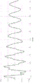
In general, the Q factor is defined as the energy stored in the resonant tank circuit 106 due to its own internal energyThe speed of the weakening by loss. If FO is present, the energy present by the bulk resonant circuit 106 fluctuates, and the Q factor changes compared to without FO. For simplicity, the resonant voltage V on the first end 132 of the inductor coil 108, which is capable of characterizing the energy stored by the resonator body circuit 106, is measuredrTo determine the Q factor. When the switches S2 and S4 are closed, the resonant voltage V can be determined on the first end 132 of the inductor coil 108r. Fig. 3 shows the resonance voltage V of the inductor coil 108 in fig. 2rA time-varying pattern.
Fig. 4 is a circuit diagram of a wireless charger 400 capable of operating in accordance with an embodiment of the present invention. The wireless charger 400 includes a voltage supply 402, an inverter 404, a filter 406, a resonator circuit 408, and a controller 410. The voltage supply 402, the inverter 404, and the resonant tank circuit 408 of the wireless charger 400 of fig. 4 are similar to the voltage supply 102, the inverter 104, and the resonant tank circuit 106 of the wireless charger 100 of fig. 1, and are only briefly described herein.
The voltage supply 402 provides a DC supply voltage on an output 412. The inverter converts the DC voltage to an AC signal and provides the AC signal to the filter 406.
Similar to the inverter 104 of fig. 1, the inverter 404 of fig. 4 is a full bridge inverter including a first branch 416 and a second branch 418. A first branch 416 and a second branch 418 are connected in parallel between the output 412 of the voltage supply 402 and ground 414. More specifically, the first branch 416 includes a first switch S1 and a second switch S2 connected in series, wherein a first terminal of the first switch S1 receives the DC supply voltage from the output terminal 412 and a terminal of the second switch S2 is connected to the ground 414. The second branch 418 comprises a third switch S3 and a fourth switch S4 connected in series, wherein a first terminal of the third switch S3 receives the DC supply voltage from the output terminal 412 and a terminal of the fourth switch S4 is connected to ground 414. The inverter has a first output 420 and a second output 422 to provide the converted AC signal to the filter 406. The first output terminal 420 is connected to a node between the first switch S1 and the second switch S2, and the second output terminal 422 is connected to a node between the third switch S3 and the fourth switch S4.
In normal operation, for example in a charging behavior, the first switch S1 and the second switch S2 in the first branch 416 are alternately closed under the control of the controller 410. Similarly, in the second branch 418, the third switch S3 and the fourth switch S4 are alternately closed as controlled by the controller 410. Switches S1 and S2, or switches S3 and S4, are not closed at the same time to avoid shorting voltage supply 402. As a result, the voltage at the output of the inverter circuit is a (square wave) AC signal, the frequency of which corresponds to the switching frequency of the switches. The switches S1-S4 of the wireless charger 400 of fig. 4 may be implemented as MOSFETs as shown in fig. 1, or as other switches controllable to be conductive.
The filter 406 is connected to the inverter 404 to receive the AC signal via a first output 420 and a second output 422. The filter 406 filters the AC signal and generates a filtered Pulse Width Modulated (PWM) signal. Here, the filter 406 is a PI-type filter (PI filter) including a first inductor L1, a second inductor L2, and a capacitor C1. The first inductor L1 is connected to the second output 422 of the inverter 404 and the second inductor L2 is connected to the first output 420 of the inverter 404. The first inductor L1 has a first end 424 connected to the second output 422 of the inverter 404, and a second end 426 connected to the resonator circuit 408 and to a first end of a capacitor C1. Similarly, the second inductor L2 has a first end 428 connected to the first output 420 of the inverter 404, and a second end 430 connected to the resonator circuit 408 and to the second end of the capacitor C1. Thus, the capacitor C1 is connected between the second end 426 of the first inductor L1 and the second end 430 of the second inductor L2. In other words, the first inductor L1 and the second inductor L2 are connected on opposite sides of the capacitor C1. According to one embodiment, the first inductor L1 and the second inductor each have an inductance value of 1 microhenry (μ H) and the capacitor C1 has a capacitance value of 0.4 microfarad (μ F). In other non-limiting embodiments, first inductor L1 and second inductor L2 each have an inductance value ranging from 0.1 μ H to 10 μ H, and capacitor C1 has a capacitance value ranging from 0.1 μ F to 2 μ F.
The PI-type filter 406 filters out higher harmonics from the square wave AC signal from the inverter 404 to generate a sine wave PWM signal, and provides the filtered sine wave PWM signal to the resonator circuit 408. In other embodiments, filter 406 may include more or fewer inductors. For example, the filter 406 may be implemented as an L-type filter including only the capacitor C1 and one of the first and second inductors L1 and L2, as compared to the PI-type filter 406 shown in fig. 4. The filter 406 makes the wireless charger 400 suitable for use in high power applications, such as power scenarios of 10 watts (W) to 60W. The frequency of the PWM signal depends on the switching frequencies of the switches S1 to S4 as described above. In an application according to the Qi protocol, the frequency of the PWM signal is between 105kHz and 210 kHz.
Similar to the resonator body 106 of fig. 1, the resonator body circuit 408 of fig. 4 is connected to the filter 406 to receive the sine wave PWM signal. Specifically, the PWM signal of the filter 406 is provided across its first and second terminals (not numbered) of the capacitor C1, and the resonator circuit 408 is connected across the capacitor C1 of the filter 406 to receive the PWM signal. The resonant tank circuit 408 includes an inductor coil L3, which transmits power. The transmitted power can be used to charge receiver devices located within the charging region of the wireless charger 400. The wireless charger 400 is also able to communicate with a receiver device, for example in the form of data packets according to the Qi standard, using the inductor coil L3 of the resonant body circuit 408.
The inductor coil L3 of the resonator body circuit 408 has a first end 432 and a second end 434, the first end 432 being coupled to the second end 426 of the first inductor L1 of the filter 406, the second end 434 being connected to the second end 430 of the second inductor L2 of the filter 406. The resonator circuit 408 also includes a capacitor C2 connected between the second end 426 of the first inductor L1 of the filter 406 and the first end 432 of the inductor coil L3. It should be appreciated that capacitor C2 is thus connected in series with inductor coil L3.
As previously described with reference to fig. 2, at the time of determination of the Q-factor, the first switch S1 and the fourth switch S4 are closed for a short time to emit an excitation current to trigger the resonator circuit 408 to oscillate. The first switch S1 and the fourth switch S4 are closed to emit the excitation currentThe time is shorter than the closing time of the switch per cycle at the moment of the normal operating phase. After the energizing current is sourced, if the wireless charger 400 operates similar to the wireless charger 100 of fig. 1, closing the switch S2 of the first branch 416 and the switch S4 of the second branch 418, and opening the switches S1 and S3, the voltage V isrIt would be difficult to measure because neither inductor coil L3 nor capacitor C2 is grounded. Conversely, inductor coil L3 and capacitor C2 are floating.
Furthermore, if switches S2 and S4 are closed, not only inductor coil L3 and capacitor C2 are coupled into the resonant network, but also first inductor L1 and second inductor L2 are coupled into the resonant network which is triggered by the excitation current to begin resonance. Thus, the plurality of resonant elements coupled into the resonant network will result in a plurality of resonant frequencies, also referred to as "poles," of the resonant network. When the inductor coil L3 and the first and second inductors L1 and L2 are both coupled into the resonant network as shown with reference to fig. 5, the waveform of the current flowing through the inductor coil L3 is complex and includes higher harmonic components, making the Q factor difficult to determine. These higher harmonics are particularly evident at the onset of resonance on the left side of the waveform, however they are seen to decay more rapidly than the fundamental resonance, so that only one harmonic, or single pole resonance, is seen in the right portion of the waveform.
Reference is now made to fig. 6, which is a signal timing diagram of control signals from the controller 410 applied to the switches S1-S4, in accordance with an embodiment of the present invention. According to this embodiment, the controller 410 controls the first to fourth switches S1 to S4 to place the wireless charger 400 in the wireless charging phase before the time t 0. As can be seen from fig. 6, during the wireless charging phase, the switch S1 and the switch S2 are alternately closed, and the switch S3 and the switch S4 are alternately closed to provide the PWM signal to the resonator circuit 408. Starting from time t0, the wireless charger 400 enters a Q-factor determination phase: to determine the Q factor, the excitation current is issued by closing the first switch S1 and the fourth switch S4 for a time t1, the time t1 being no longer than the closing time of the switches in each cycle in the wireless charging phase.
At an excitation current, also known asAfter the current pulse is sent, all switches S1, S2, S3, S4 are opened at time t 2. It can be seen that since all the switches are open, the inductor coil L3, the capacitor C2 of the resonator circuit 408, and the capacitor C1 of the filter 406 are connected as a resonant network, which is triggered by the excitation current to start resonating. The resonant network includes only inductor coil L3, capacitor C2, and capacitor C1, such that the resonant elements inductor L1 and inductor L2 are reduced in the resonant network, thereby removing additional poles from the resonant signal. The simplified resonant network achieves the simplified and clear resonant current I shown in FIG. 6rWhich is shown in more detail in fig. 7, and makes it easy to determine the Q factor.
Fig. 8 is a circuit diagram of a wireless charger 800 according to an embodiment. Similar to the wireless charger 400 shown in fig. 4, the wireless charger 800 of fig. 8 includes a voltage supply 802, an inverter 804, a filter 806, a resonator circuit 808, and a controller 810, all of which are similarly named and numbered and are not described in detail herein. In addition, the wireless charger 800 further includes a current sensor 840, the current sensor 840 coupled between the second end 834 of the inductor coil L3 of the resonator circuit 808 and the capacitor C1 of the filter 806. Thus, the current sensor 840, the inductor coil L3 of the resonator circuit 808, and the capacitor C2 are connected in series. Current sensor 840 provides an output current IrWhich characterizes the current flowing through the third inductor coil L3. It should be understood that the output current IrCharacterizing the aforementioned voltage VrAnd may further be used to calculate the Q factor by known formulas and/or equations. In the embodiment shown in FIG. 8, Current sensor 840 is a Current Transformer (CT) having a winding ratio of, for example, 1: 100, where the primary winding of CT840 is coupled in resonant tank circuit 808 and the secondary winding of CT840 is coupled to provide output Current Ir. It can be appreciated that the primary winding of the current sensor 840 coupled into the wireless charger 800 is a nearly pure conductor, introducing little to no poles in the resonant network.
In the normal power transmission phase (wireless charging phase), wireless charging is performedThe power loss between the power transmitted by the device 800 and the power received by the receiver device is typically used to determine whether there is a foreign object in the charging area. The power emitted by the wireless charger 800 may also use the current I detected by the current sensor 840rTo calculate. As such, coupling the current sensor 840 into the wireless charger 800 further facilitates determining power loss and facilitates Foreign Object Detection (FOD) during power transfer phases.
Various exemplary embodiments are described herein with reference to specific illustrated examples. The examples are chosen to assist those skilled in the art in forming a clear understanding of, and enabling description for, the various embodiments. However, the scope of systems, structures, and devices that may be constructed to include one or more embodiments, and the scope of methods that may be implemented in accordance with one or more embodiments, is not intended to be limited by the illustrative examples shown. Rather, those skilled in the art will understand based on the present description that: many other configurations, structures and methods can be implemented in accordance with the embodiments.
It will be appreciated that with respect to the various positional indications used in the preceding description of the invention, such as top, bottom, upper and lower, those indications are given with reference to the corresponding figures only and may instead have other positional relationships as the orientation of the device changes during manufacture or operation. As mentioned above, those positional relationships are described for clarity only and are not limiting.
The foregoing description of the present specification refers to particular embodiments and to particular drawings, but the invention should not be limited thereto but should be given by the claims. The drawings described are only exemplary and are non-limiting. In the drawings, the size of various elements may be exaggerated and not drawn on a particular scale for illustrative purposes. The present description should also include discrete variations in the tolerances and properties of the various components, modes of operation. Various weakening implementations of the present invention should also be included.
The word "comprising" as used in the present description and claims does not exclude other elements or steps. Where the singular forms "a", "an" and "the" refer to an element that is definite or indefinite, the plural of that element is intended to be included, unless the context clearly dictates otherwise. Thus, the word "comprising" should not be construed as being limited to the items listed thereafter, nor should it be construed as including other elements or steps; the scope of the description "a device includes items a and B" should not be limited to devices that include only elements a and B. This description indicates that, for the purposes of this description, only elements a and B of the device are relevant. Although coupling generally includes an inductive connection, a connection generally meaning a connection through, for example, a wire, the terms "connected," "coupled," and "coupled" herein mean that there is electrical communication between the coupled or connected elements, and do not mean that there are no intervening elements between them. In describing transistors and their connections, the terms gate, drain, and source are interchangeable with gate, drain, source, and gate terminals, drain terminals, source terminals.
It will be apparent to those skilled in the art that various changes in detail may be made therein without departing from the scope of the invention as defined in the appended claims.

Claims (10)

1.一种确定无线充电器的品质因数的方法,其中无线充电器包括逆变器、滤波器、以及谐振体电路;逆变器配置为接收供电电压,以及通过开合逆变器的第一开关、第二开关、第三开关、及第四开关来产生PWM信号;滤波器连接到逆变器,以及配置为接收PWM信号、产生经滤波的信号;谐振体电路连接到滤波器,以及配置为接收经滤波的信号、在无线充电器的无线充电阶段向接收器提供无线电能;其特征在于,所述方法包括:1. A method of determining a quality factor of a wireless charger, wherein the wireless charger includes an inverter, a filter, and a resonant body circuit; the inverter is configured to receive a supply voltage, and a first a switch, a second switch, a third switch, and a fourth switch to generate the PWM signal; the filter is connected to the inverter and configured to receive the PWM signal and generate a filtered signal; the resonator circuit is connected to the filter, and configured For receiving the filtered signal, providing wireless power to the receiver during the wireless charging phase of the wireless charger; characterized in that the method comprises: 闭合第一开关和第二开关的一者,以及闭合第三开关和第四开关的一者,以向谐振体电路发出电流脉冲;以及closing one of the first switch and the second switch and closing one of the third switch and the fourth switch to issue a current pulse to the resonant body circuit; and 在无线充电器的Q因数确定阶段,打开第一开关至第四开关。In the Q-factor determination stage of the wireless charger, the first to fourth switches are turned on. 2.根据权利要求1所述的方法,其特征在于,进一步包括,通过以下来将逆变器连接为全桥类型的逆变器:2. The method of claim 1, further comprising connecting the inverter as a full-bridge type inverter by: 将第一开关和第二开关串联作为第一分支;Connect the first switch and the second switch in series as the first branch; 将第三开关和第四开关串联作为第二分支;以及connecting the third switch and the fourth switch in series as a second branch; and 将第一分支和第二分支并联连接在电压供应器与地之间。The first branch and the second branch are connected in parallel between the voltage supply and ground. 3.根据权利要求1所述的方法,其特征在于,进一步包括,通过以下来将滤波器连接为PI型滤波器:3. The method of claim 1, further comprising, connecting the filter as a PI-type filter by: 将电感器的第一端连接到逆变器以接收PWM信号;以及connecting the first end of the inductor to the inverter to receive the PWM signal; and 将电容器连接到电感器的第二端,其中经滤波的信号跨电容器而被提供。A capacitor is connected to the second end of the inductor, wherein the filtered signal is provided across the capacitor. 4.一种确定无线充电器的品质因数的方法,其特征在于,无线充电器包括:4. A method for determining a quality factor of a wireless charger, wherein the wireless charger comprises: 逆变器,配置为接收供电电压,以及在第一节点和第二节点上产生PWM信号;an inverter configured to receive the supply voltage and generate a PWM signal on the first node and the second node; 滤波器,连接到逆变器的第一节点和第二节点以接收PWM信号,以及在电容器的第一端和第二端上产生经滤波的信号;以及a filter connected to the first and second nodes of the inverter to receive the PWM signal, and to generate a filtered signal on the first and second ends of the capacitor; and 谐振器网络,连接到滤波器的电容器的第一端和第二端以接收经滤波的信号,以及配置为在电感器线圈向接收器提供无线电能;以及其中所述方法包括:a resonator network connected to first and second ends of a capacitor of the filter to receive the filtered signal, and configured to provide wireless power to the receiver at the inductor coil; and wherein the method includes: 向谐振体电路发出电流脉冲;以及sending a current pulse to the resonator circuit; and 在无线充电器的Q因数确定阶段,将谐振体电路和滤波器的电容器连接到谐振网络。In the Q-factor determination stage of the wireless charger, connect the resonant body circuit and the capacitor of the filter to the resonant network. 5.根据权利要求4所述的方法,其特征在于,进一步包括:5. The method of claim 4, further comprising: 通过将第一分支和第二分支并联连接在电压供电器和地之间来将逆变器连接为全桥类型逆变器,其中第一分支包括串联连接的第一开关和第二开关,第二分支包括串联连接的第三开关和第四开关;The inverter is connected as a full-bridge type inverter by connecting a first branch and a second branch in parallel between the voltage supply and ground, wherein the first branch includes a first switch and a second switch connected in series, the first The second branch includes a third switch and a fourth switch connected in series; 闭合第一开关和第二开关之一,以及闭合第三开关和第四开关之一,以在第一开关和第二开关之间的第一节点与第三开关和第四开关之间的第二节点上提供电流脉冲;以及Closing one of the first switch and the second switch, and closing one of the third switch and the fourth switch, to the first node between the first switch and the second switch and the first node between the third switch and the fourth switch current pulses are provided on the two nodes; and 在无线充电器的Q因数确定阶段,打开逆变器的第一开关至第四开关,以将谐振体电路和滤波器的电容器连接为谐振网络。In the Q-factor determination stage of the wireless charger, the first to fourth switches of the inverter are turned on to connect the resonant body circuit and the capacitor of the filter as a resonant network. 6.根据权利要求4所述的方法,其特征在于,进一步包括,通过以下来将滤波器连接为PI型滤波器:6. The method of claim 4, further comprising, connecting the filter as a PI-type filter by: 将电感器的第一端连接到逆变器的第一节点以接收PWM信号;以及connecting the first end of the inductor to the first node of the inverter to receive the PWM signal; and 将电容器连接到电感器的第二端。Connect the capacitor to the second end of the inductor. 7.根据权利要求4所述的方法,其特征在于,进一步包括:7. The method of claim 4, further comprising: 将电感器线圈和电容器跨滤波器的电容器而串联连接,以将谐振体电路连接到滤波器的电容器的第一端和第二端,来接收经滤波的信号,其中谐振体电路的电容器连接在电感器线圈和滤波器的电容器之间;以及The inductor coil and capacitor are connected in series across the capacitor of the filter to connect the resonant body circuit to the first and second ends of the capacitor of the filter to receive the filtered signal, wherein the capacitor of the resonant body circuit is connected at between the inductor coil and the filter capacitor; and 将谐振体电路的电感器线圈和电容器与电流传感器串联,其中电流传感器配置为产生表征流经电感器线圈的电流的电流信号。The inductor coil and capacitor of the resonant body circuit are connected in series with a current sensor, wherein the current sensor is configured to generate a current signal representative of the current flowing through the inductor coil. 8.一种无线充电器,其特征在于,包括:8. A wireless charger, comprising: 逆变器,配置为从电压供应器接收供电电压及产生PWM信号,其中逆变器包括并联连接在电压供应器与地之间的第一分支和第二分支,以及其中第一分支包括串联连接的第一开关和第二开关,第二分支包括串联连接的第三开关和第四开关;an inverter configured to receive a supply voltage from a voltage supply and generate a PWM signal, wherein the inverter includes a first branch and a second branch connected in parallel between the voltage supply and ground, and wherein the first branch includes a series connection The first switch and the second switch, the second branch includes the third switch and the fourth switch connected in series; 滤波器,连接到逆变器以接收PWM信号,以及配置为产生经滤波的信号,其中滤波器包括电容器和连接到电容器的电感器;a filter connected to the inverter to receive the PWM signal and configured to generate a filtered signal, wherein the filter includes a capacitor and an inductor connected to the capacitor; 谐振体电路,跨滤波器的电容器连接以接收经滤波的信号,其中谐振体电路配置为在无线充电阶段向位于无线充电器的充电区域的接收器提供无线电能;以及a resonator circuit connected across a capacitor of the filter to receive the filtered signal, wherein the resonator circuit is configured to provide wireless power to a receiver located in a charging area of the wireless charger during the wireless charging phase; and 控制器,连接到逆变器的第一开关至第四开关,以及配置为:a controller, connected to the first to fourth switches of the inverter, and configured to: 闭合第一开关和第二开关之一,以及闭合第三开关和第四开关之一,以向谐振体电路发出电流脉冲;以及closing one of the first switch and the second switch and closing one of the third switch and the fourth switch to send a current pulse to the resonant body circuit; and 在无线充电器的Q因数确定阶段,打开第一开关和第四开关。In the Q-factor determination stage of the wireless charger, the first switch and the fourth switch are turned on. 9.根据权利要求8所述的无线充电器,其特征在于:逆变器配置为在第一开关和第二开关之间的第一节点、以及第三开关和第四开关之间的第二节点提供PWM信号;以及其中滤波器连接到逆变器的第一节点和第二节点以接收PWM信号。9. The wireless charger of claim 8, wherein the inverter is configured as a first node between the first switch and the second switch, and a second node between the third switch and the fourth switch The node provides the PWM signal; and wherein the filter is connected to the first node and the second node of the inverter to receive the PWM signal. 10.根据权利要求8所述的无线充电器,其特征在于:谐振体电路包括串联连接的电感器线圈和电容器,电感器线圈配置为提供无线电能。10. The wireless charger of claim 8, wherein the resonant body circuit includes an inductor coil and a capacitor connected in series, the inductor coil being configured to provide wireless power.
CN201911254542.0A 2019-12-06 2019-12-06 Method for determining quality factor and wireless charger Pending CN112928825A (en)

Priority Applications (2)

Application Number Priority Date Filing Date Title
CN201911254542.0A CN112928825A (en) 2019-12-06 2019-12-06 Method for determining quality factor and wireless charger
US17/104,163 US11990781B2 (en) 2019-12-06 2020-11-25 Method for determining a quality factor and wireless charger

Applications Claiming Priority (1)

Application Number Priority Date Filing Date Title
CN201911254542.0A CN112928825A (en) 2019-12-06 2019-12-06 Method for determining quality factor and wireless charger

Publications (1)

Publication Number Publication Date
CN112928825A true CN112928825A (en) 2021-06-08

Family

ID=76162166

Family Applications (1)

Application Number Title Priority Date Filing Date
CN201911254542.0A Pending CN112928825A (en) 2019-12-06 2019-12-06 Method for determining quality factor and wireless charger

Country Status (2)

Country Link
US (1) US11990781B2 (en)
CN (1) CN112928825A (en)

Cited By (1)

* Cited by examiner, † Cited by third party
Publication number Priority date Publication date Assignee Title
CN113824495A (en) * 2021-11-23 2021-12-21 深圳维普创新科技有限公司 Circuit, method and device for calculating Q-Factor and electronic equipment

Families Citing this family (10)

* Cited by examiner, † Cited by third party
Publication number Priority date Publication date Assignee Title
CN112928825A (en) 2019-12-06 2021-06-08 恩智浦美国有限公司 Method for determining quality factor and wireless charger
EP4016798B1 (en) * 2020-12-17 2025-09-17 Stichting IMEC Nederland A powering apparatus for wireless powering and a method for controlling a powering apparatus
CN113472094B (en) * 2021-08-13 2024-07-26 上海伏达半导体有限公司 Wireless charging transmitting device, resonant circuit, quality factor detection method and processor
US11916406B1 (en) 2021-09-16 2024-02-27 Apple Inc. Techniques for wireless power systems power delivery
US20230163635A1 (en) * 2021-11-19 2023-05-25 Samsung Electronics Co., Ltd. Wireless power transmission device and operating method of wireless power transmitter
CN114252702B (en) * 2021-11-23 2024-09-20 深圳维普创新科技有限公司 Quality factor detection circuit, method and device and electronic equipment
CN116610192B (en) * 2022-02-09 2024-04-05 荣耀终端有限公司 Electronic equipment and method for judging presence of handwriting pen
CN117375255A (en) * 2022-06-30 2024-01-09 恩智浦有限公司 Wireless charging transmitter and method of operation
US20240291395A1 (en) * 2023-02-24 2024-08-29 Molex, Llc Bridge inverters for wireless charging
CN117129763A (en) * 2023-04-24 2023-11-28 荣耀终端有限公司 Stylus offset detection method and electronic device

Citations (4)

* Cited by examiner, † Cited by third party
Publication number Priority date Publication date Assignee Title
CN104701999A (en) * 2015-03-27 2015-06-10 南京矽力杰半导体技术有限公司 Resonance type noncontact power supply device, electricity energy emission end and control method
US20160134131A1 (en) * 2013-07-19 2016-05-12 Ihi Corporation Power-supplying device and wireless power-supplying system
US10199881B2 (en) * 2015-10-23 2019-02-05 Mediatek Inc. Robust foreign objects detection
US20190217726A1 (en) * 2016-07-19 2019-07-18 Grant Anthony Covic Electric vehicle detection for roadway wireless power transfer

Family Cites Families (98)

* Cited by examiner, † Cited by third party
Publication number Priority date Publication date Assignee Title
AT331912B (en) 1973-09-20 1976-08-25 Rodler Ing Hans DEVICE FOR MEASURING THE DAMPING FACTORS OF VIBRANT CIRCUITS AND FOR MEASURING THE LOCAL CLOSURES IN COILS
US5420518A (en) 1993-09-23 1995-05-30 Schafer, Jr.; Kenneth L. Sensor and method for the in situ monitoring and control of microstructure during rapid metal forming processes
US6471106B1 (en) 2001-11-15 2002-10-29 Intellectual Property Llc Apparatus and method for restricting the discharge of fasteners from a tool
US6822425B2 (en) * 2002-01-25 2004-11-23 Vector Products, Inc. High frequency battery charger and method of operating same
US6831423B2 (en) 2003-03-28 2004-12-14 General Electric Company High Q impedance matching inverter circuit with automatic line regulation
EP1634355B1 (en) * 2003-05-23 2018-10-10 Auckland Uniservices Limited Methods and apparatus for control of inductively coupled power transfer systems
JP4494426B2 (en) 2007-02-16 2010-06-30 セイコーエプソン株式会社 Power transmission control device, power reception control device, non-contact power transmission system, power transmission device, power reception device, and electronic equipment
JP2009027781A (en) 2007-07-17 2009-02-05 Seiko Epson Corp Power reception control device, power reception device, non-contact power transmission system, charge control device, battery device, and electronic device
TW200919901A (en) 2007-10-24 2009-05-01 Jay Digidata Internat Co Ltd Control integrated circuit and energy transmission circuit applying the same
US9178387B2 (en) 2008-05-13 2015-11-03 Qualcomm Incorporated Receive antenna for wireless power transfer
SG177292A1 (en) 2009-06-19 2012-02-28 Cohda Wireless Pty Ltd Characterisation of a wireless communications link
CN102823101B (en) 2010-02-08 2015-06-17 捷通国际有限公司 Input parasitic metal detection
US9853478B2 (en) 2010-07-28 2017-12-26 Qualcomm Incorporated Low power detection of wireless power devices
NZ587357A (en) * 2010-08-13 2013-03-28 Auckland Uniservices Ltd Control circuit for pick-up in inductive power transfer system selectively shunts diodes in rectifier bridge to reduce transient disturbances to primary current
US9294153B2 (en) 2010-09-23 2016-03-22 Texas Instruments Incorporated Systems and methods of wireless power transfer with interference detection
US8983374B2 (en) 2010-12-13 2015-03-17 Qualcomm Incorporated Receiver for near field communication and wireless power functionalities
WO2012127335A1 (en) 2011-03-21 2012-09-27 Koninklijke Philips Electronics N.V. Calculating power loss for inductive power transmission
US8890368B2 (en) * 2011-06-27 2014-11-18 Maxim Integrated Products, Inc. Systems and methods for power transfer based on resonance coupling of inductors
JP5071574B1 (en) * 2011-07-05 2012-11-14 ソニー株式会社 Sensing device, power receiving device, non-contact power transmission system, and sensing method
CN103959597A (en) * 2011-08-26 2014-07-30 Lg伊诺特有限公司 Wireless power transmitter and wireless power transmission method
DE102011112873A1 (en) * 2011-09-08 2013-03-14 Giesecke & Devrient Gmbh Method for testing an antenna coil
WO2013036947A2 (en) 2011-09-09 2013-03-14 Witricity Corporation Foreign object detection in wireless energy transfer systems
JP5940784B2 (en) 2011-09-09 2016-06-29 国立大学法人埼玉大学 Non-contact power feeding device for moving objects
JP5927826B2 (en) * 2011-09-28 2016-06-01 日産自動車株式会社 Contactless power supply
US9553485B2 (en) 2011-10-13 2017-01-24 Integrated Device Technology, Inc. Apparatus, system, and method for detecting a foreign object in an inductive wireless power transfer system based on input power
US9450648B2 (en) * 2011-10-13 2016-09-20 Integrated Device Technology, Inc. Apparatus, system, and method for detecting a foreign object in an inductive wireless power transfer system
DE102011086849A1 (en) * 2011-11-22 2013-05-23 Funkwerk Dabendorf-Gmbh Charging circuit for an energy store of a portable electrical device
KR101951358B1 (en) 2011-12-15 2019-02-22 삼성전자주식회사 Wireless power transmitter, wireless power receiver and method for controlling each thereof
EP2807662A4 (en) * 2012-01-23 2015-06-17 Univ Utah State Wireless power transfer system
US9410823B2 (en) 2012-07-13 2016-08-09 Qualcomm Incorporated Systems, methods, and apparatus for detection of metal objects in a predetermined space
US9287040B2 (en) * 2012-07-27 2016-03-15 Thoratec Corporation Self-tuning resonant power transfer systems
US9154189B2 (en) * 2012-08-17 2015-10-06 Qualcomm Incorporated Wireless power system with capacitive proximity sensing
US9178361B2 (en) * 2012-09-27 2015-11-03 ConvenientPower, Ltd. Methods and systems for detecting foreign objects in a wireless charging system
WO2014054953A1 (en) * 2012-10-01 2014-04-10 Auckland Uniservices Limited Inductive power transfer control using energy injection
US9404954B2 (en) 2012-10-19 2016-08-02 Witricity Corporation Foreign object detection in wireless energy transfer systems
CN110098642A (en) 2012-11-05 2019-08-06 苹果公司 Inductively electrical power transmission system
JP5741962B2 (en) * 2012-11-30 2015-07-01 株式会社デンソー Non-contact power feeding device
RU2656613C2 (en) * 2013-01-11 2018-06-06 Конинклейке Филипс Н.В. Wireless inductive power transfer
EP2954338B1 (en) * 2013-02-07 2020-04-15 Giesecke+Devrient Mobile Security GmbH Method and device for testing a circuit
US9287718B2 (en) 2013-03-01 2016-03-15 Nokia Technologies Oy Method, apparatus, and computer program product for foreign object detection parameter and charging data communication with wireless charging capable battery pack
KR102003358B1 (en) 2013-03-22 2019-07-24 삼성전자주식회사 Wireless power transmitter, wireless power receiver and method for controlling each thereof
KR102187962B1 (en) 2013-05-10 2020-12-08 삼성전자주식회사 Differential load detection method for detecting a wireless power receiver in wireless power network and wireless power transmitter
CN107968493B (en) 2013-06-05 2021-07-23 三星电子株式会社 Wireless power receiver, wireless power transmitter and control method thereof
CN105027387B (en) * 2013-07-31 2018-03-13 松下电器产业株式会社 Wireless power transmission device and Wireless power transmission system
CN103852631A (en) 2014-01-11 2014-06-11 深圳市普林泰克科技有限公司 Algorithm for indirectly detecting metal foreign bodies for wireless charger
US9685815B2 (en) 2014-01-16 2017-06-20 Mediatek Inc. Method for performing wireless charging control with aid of admittance detection, and associated apparatus
US10283995B2 (en) 2014-02-28 2019-05-07 L'oreal Charge current monitoring or control in a resonance-tuned inductive charger
US9735585B2 (en) * 2014-05-05 2017-08-15 Google Inc. Foreign object detection method for wireless charging systems
US10122220B2 (en) * 2014-06-18 2018-11-06 WIPQTUS Inc. Wireless power system for portable devices under rotational misalignment
EP3034002B1 (en) * 2014-12-18 2017-03-29 Schleifring und Apparatebau GmbH Inductive rotary joint with multimode inverter
US9614395B2 (en) 2014-12-30 2017-04-04 Automotive Research & Testing Center Wireless charging system and foreign metal object detection method for the system
CN106160253B (en) * 2015-03-13 2020-09-04 恩智浦美国有限公司 Free resonance analog exploration for wireless power transfer
US9474031B1 (en) 2015-04-16 2016-10-18 Freescale Semiconductor, Inc. Method and system for performing foreign object detection in an inductive wireless power transfer system
US20160336809A1 (en) 2015-05-12 2016-11-17 Powermat Technologies Ltd. System and methods for sensor based coil monitoring of a wireless power receiver
US10566839B2 (en) * 2015-06-30 2020-02-18 WiTricinity Corporation Systems, methods and apparatus for guidance and alignment between electric vehicles and wireless charging systems
CN205027804U (en) 2015-08-05 2016-02-10 艾默生网络能源系统北美公司 Current detection circuit and power supply circuit of totem -pote circuit
US10248899B2 (en) * 2015-10-06 2019-04-02 Witricity Corporation RFID tag and transponder detection in wireless energy transfer systems
US10581281B2 (en) * 2015-10-23 2020-03-03 Mediatek Inc. In situ coil parameter measurements and foreign objects detection
RU2696491C1 (en) * 2015-11-25 2019-08-02 Конинклейке Филипс Н.В. Wireless inductive power transmission
CN107026516B (en) 2016-02-01 2022-04-05 恩智浦美国有限公司 Receiver removal detection in wireless charging systems
EP3420629B1 (en) * 2016-02-24 2019-06-19 Koninklijke Philips N.V. Wireless inductive power transfer
CN107204699B (en) * 2016-03-15 2021-05-07 恩智浦美国有限公司 Determination of Q Factor of Resonant Energy Storage Network
CN109952503B (en) * 2016-07-01 2022-09-09 Lg伊诺特有限公司 Method and apparatus and system for detecting foreign objects
US20180048162A1 (en) * 2016-08-15 2018-02-15 Qualcomm Incorporated Methods and apparatus for signaling using harmonic and subharmonic modulation
CN106685206A (en) * 2016-08-31 2017-05-17 株式会社村田制作所 Power-factor correction device and control method thereof and electronic device
CN107994685B (en) 2016-10-26 2023-11-24 恩智浦美国有限公司 Foreign object detection
KR20180046018A (en) * 2016-10-27 2018-05-08 엘지이노텍 주식회사 Wireless charging coil of apparatus for transmitting and receiving wireless power and thereof production method
JP6784170B2 (en) * 2016-12-27 2020-11-11 Tdk株式会社 Metal foreign matter detector, wireless power supply device, wireless power receiving device, and wireless power transmission system
US9919610B1 (en) * 2017-01-12 2018-03-20 The Florida International University Board Of Trustees Wireless power electronics and controls
US10511197B2 (en) * 2017-02-02 2019-12-17 Apple Inc. Wireless charging system with object detection
SG10201708902RA (en) * 2017-02-02 2018-09-27 Apple Inc Wireless Charging System With Object Detection
US10770921B2 (en) * 2017-02-10 2020-09-08 Apple Inc. Wireless charging system with start-up negotiation
US10427532B2 (en) * 2017-04-05 2019-10-01 Ford Global Technologies, Llc On-board and wireless vehicle charging systems with shared components
US10308123B2 (en) * 2017-04-19 2019-06-04 Witricity Corporation Vehicle-side beacon mode for wireless electric vehicle charging
US10320241B2 (en) * 2017-05-17 2019-06-11 Apple Inc. Wireless charging system with object recognition
US11043853B2 (en) * 2017-05-17 2021-06-22 Apple Inc. Wireless charging system having measurement circuitry with foreign object detection capabilities
US10804750B2 (en) * 2017-08-17 2020-10-13 Integrated Device Technology, Inc. Q-factor detection method
US10797535B2 (en) * 2017-10-09 2020-10-06 Integrated Device Technology, Inc. Q-factor measurement
CN109921524B (en) 2017-12-12 2024-08-09 恩智浦美国有限公司 Wireless charging system with power level calculation circuit for foreign matter detection
US10826325B2 (en) * 2018-02-21 2020-11-03 X2 Power Technologies Limited Hybrid control apparatus and method
US20190312459A1 (en) * 2018-04-05 2019-10-10 Apple Inc. Wireless Power System With Low Power Mode Switching
US20190326782A1 (en) * 2018-04-24 2019-10-24 Apple Inc. Wireless Charging System With Metallic Object Detection
JP6962272B2 (en) * 2018-05-18 2021-11-05 トヨタ自動車株式会社 Contactless power transmission equipment and power transmission system
US20210273492A1 (en) * 2018-06-27 2021-09-02 Powermat Technologies Ltd. Enhanced method for foreign objects detection
EP3818620A4 (en) * 2018-07-19 2022-03-23 MediaTek Singapore Pte. Ltd. DETECTION OF FOREIGN OBJECTS IN WIRELESS POWER TRANSMISSION SYSTEMS
US12506369B2 (en) * 2018-09-06 2025-12-23 Auckland Uniservices Limited Inductive power and data transfer using energy injection
CN111313569A (en) * 2018-12-11 2020-06-19 恩智浦美国有限公司 Q Factor Determination of Foreign Object Detection Circuit in Wireless Charging System
CN111371189B (en) * 2018-12-26 2024-06-25 恩智浦美国有限公司 Determining the Q Factor in Wireless Charging Systems with Complex Resonant Circuits
KR102649852B1 (en) * 2019-12-03 2024-03-22 애플 인크. Wireless power systems that detect foreign substances
CN112928825A (en) 2019-12-06 2021-06-08 恩智浦美国有限公司 Method for determining quality factor and wireless charger
US11316383B1 (en) * 2019-12-10 2022-04-26 Apple Inc. Wireless power systems with foreign object detection
US11909198B2 (en) * 2020-01-29 2024-02-20 Witricity Corporation Gate driver implementations for safe wireless power system operation
US11271393B1 (en) * 2020-08-31 2022-03-08 Stmicroelectronics Asia Pacific Pte Ltd Advanced protection circuit for Q factor sensing pad
EP3961899B1 (en) * 2020-08-31 2023-11-22 STMicroelectronics S.r.l. Quality factor estimation of an inductive element
US11218026B1 (en) * 2020-09-17 2022-01-04 Utah State University Zero-crossing current detection for modular and robust dynamic wireless power transfer
WO2022066278A1 (en) * 2020-09-25 2022-03-31 Apple Inc. Efficient wireless power transfer control
TWI759972B (en) * 2020-11-25 2022-04-01 偉詮電子股份有限公司 Wireless power transfer systems and control methods thereof for quick object detection
US11979036B2 (en) * 2020-12-30 2024-05-07 Ut-Battelle, Llc System and method of wireless power supply

Patent Citations (4)

* Cited by examiner, † Cited by third party
Publication number Priority date Publication date Assignee Title
US20160134131A1 (en) * 2013-07-19 2016-05-12 Ihi Corporation Power-supplying device and wireless power-supplying system
CN104701999A (en) * 2015-03-27 2015-06-10 南京矽力杰半导体技术有限公司 Resonance type noncontact power supply device, electricity energy emission end and control method
US10199881B2 (en) * 2015-10-23 2019-02-05 Mediatek Inc. Robust foreign objects detection
US20190217726A1 (en) * 2016-07-19 2019-07-18 Grant Anthony Covic Electric vehicle detection for roadway wireless power transfer

Cited By (1)

* Cited by examiner, † Cited by third party
Publication number Priority date Publication date Assignee Title
CN113824495A (en) * 2021-11-23 2021-12-21 深圳维普创新科技有限公司 Circuit, method and device for calculating Q-Factor and electronic equipment

Also Published As

Publication number Publication date
US11990781B2 (en) 2024-05-21
US20210175728A1 (en) 2021-06-10

Similar Documents

Publication Publication Date Title
CN112928825A (en) Method for determining quality factor and wireless charger
US7999414B2 (en) Apparatus and method for wireless energy and/or data transmission between a source device and at least one target device
JP5393083B2 (en) Apparatus and method for wireless transmission of energy and / or data between a source device and at least one target device
JP5647179B2 (en) Inductive power supply apparatus having device identification function
CN111371189B (en) Determining the Q Factor in Wireless Charging Systems with Complex Resonant Circuits
EP4290540A1 (en) Magnetic resonance-type wireless power feeding device
CN107529346A (en) Induction power transmitter
KR20170007744A (en) Wireless power transfer system
CN106160253B (en) Free resonance analog exploration for wireless power transfer
WO2018123767A1 (en) Wireless power supply device, wireless power receiving device, and wireless power transmission system
JP2016540479A (en) Wireless transmission of line frequency and line voltage AC
CN109245333A (en) A kind of constant current output radio energy transmission system that anti-excursion capability can be improved
CN104040863A (en) Methods used to control converters
JP2018107946A (en) Metal foreign substance detection device, wireless power supply device, wireless power receiving device, and wireless power transmission system
CN110506364A (en) Magnetic field generation circuit
CN102439834B (en) Electromagnetic apparatus using shared flux in a multi-load parallel magnetic circuit and method of operation
EP4300772A1 (en) Wireless charging transmitter and method of operating the same
JP6053597B2 (en) Non-contact power feeding device
EP3769411B1 (en) Determining system parameters of a contactless electrical energy transfer system
JP2019213267A (en) Non-contact transmission apparatus
CN108183558A (en) The tuning methods and equipment of resonance type wireless electric energy transmission based on phase observation
KR20150124918A (en) Power supply and method for controlling a power supply
JP2011176981A (en) Inverter circuit
CN112448482A (en) Non-contact power supply device and power transmission device
Cheng et al. A resonant frequency tracking circuit for a low-coupling-coefficient piezoelectric transducer

Legal Events

Date Code Title Description
PB01 Publication
PB01 Publication
SE01 Entry into force of request for substantive examination