Disclosure of Invention
In view of the above drawbacks and deficiencies of the prior art, an object of the present application is to provide an automatic detection apparatus and an automatic detection method for electronic products.
In order to solve the technical problem, the application is realized by the following technical scheme:
the application provides an automatic check out test set of electronic product includes:
the switching device comprises a turnover mechanism and a turnover mechanism, and is arranged on the rack;
the turnover mechanism comprises a three-dimensional movement mechanism and a bearing platform for bearing an electronic product, and the bearing platform moves in a three-dimensional space under the driving action of the three-dimensional movement mechanism;
the turnover mechanism comprises a turnover driving mechanism and a clamping part for clamping the electronic product, and the clamping part is arranged on an installation shaft of the turnover driving mechanism;
and the photographing device is installed on the rack, faces the switching device and is used for photographing the electronic product placed on the bearing platform.
Further, the above automatic detection device for electronic products, wherein the photographing apparatus includes: and the first area-array camera is arranged on the frame.
Further, the above automatic detection device for electronic products, wherein the photographing apparatus further comprises: and the camera bellows light source is arranged on the rack and matched with the first area array camera.
Further, in the automatic detection device of the electronic product, the light source of the dark box has a plurality of light emitting surfaces, and each light emitting surface is of a matte surface structure.
Further, in the automatic detection device of the electronic product, the light source of the dark box is an integrated light source.
Further, the above automatic detection device for electronic products, wherein the photographing apparatus further comprises: a second area-array camera mounted on the frame.
Further, the above automatic detection device for electronic products, wherein the photographing apparatus further comprises: the area array light source is installed on the rack and is matched with the second area array camera.
Further, the above automatic detection device for electronic products, wherein the photographing apparatus includes: a first line-scan camera mounted on the frame.
Further, the above automatic detection device for electronic products, wherein the photographing apparatus further comprises: a first line scan light source mounted on the frame, the first line scan light source disposed between the first line scan camera and the switching device.
Further, the above automatic detection device for electronic products, wherein the photographing apparatus includes: a second line scan camera also mounted on the frame.
Further, the above automatic detection device for electronic products, wherein the photographing apparatus further comprises: a second linear-scan light source mounted on the chassis, the second linear-scan light source disposed between the second linear-scan camera and the switching device.
Furthermore, the automatic detection equipment for the electronic products further comprises a clamping mechanism used for arranging and adjusting the electronic products, and the clamping mechanism is installed on the rack.
Further, the above automatic detection device for electronic products, wherein the clamping mechanism comprises:
the base is provided with a placing plane, and the placing plane is used for placing the electronic product;
the first clamping jaw and the second clamping jaw are respectively arranged on two sides of the base, and are matched with each other to clamp or release the electronic product;
the clamping driving mechanism is provided with a first sliding block and a second sliding block, the first sliding block and the second sliding block move in opposite directions or in opposite directions under the driving action of the clamping driving mechanism, and the first clamping jaw and the second clamping jaw are respectively installed on the first sliding block and the second sliding block.
Further, the above automatic detection equipment for electronic products, wherein the clamping mechanism further comprises: and the sensor is used for detecting the electronic product and is arranged close to the upper part of the placing plane.
Further, the automatic detection equipment for the electronic product is characterized in that the first clamping jaw is provided with a first clamping surface, the second clamping jaw is provided with a second clamping surface, and the first clamping surface and the second clamping surface are opposite and parallel to each other.
Further, in the automatic detection device for electronic products, a buffer layer structure is arranged on the first clamping surface/the second clamping surface.
Further, the automatic detection equipment for electronic products is described above, wherein the first clamping jaw and the second clamping jaw are made of a flexible material or an elastic material.
Further, the automatic detection equipment for electronic products described above further includes a first dust removing device disposed above the clamping device and blowing out a high-pressure gas with ions to act on the electronic products, and the first dust removing device includes: the first ion generator and the first air source conveying channel are communicated with the first ion generator.
Further, the automatic detection equipment for electronic products, wherein the first dust removing device further comprises a first air knife, and the first air knife is arranged close to the outlet of the first ion generator.
Further, the above automatic detection equipment for electronic products further comprises a second dust removal device, which is disposed above the switching device and blows out high-pressure gas with ions to act on the electronic products, wherein the second dust removal device comprises: the second ion generator and a second air source conveying channel are communicated with the second ion generator.
Further, the automatic detection equipment for electronic products, wherein the second dust removing device further comprises a second air knife, and the second air knife is arranged close to the outlet of the second ion generator.
Further, in the automatic detection equipment for electronic products, the support platform includes a support portion and an RO shaft driving mechanism for driving the support portion to turn over, and the RO shaft driving mechanism is mounted on the three-dimensional movement mechanism.
Further, in the automatic detection device for electronic products, at least one suction cup is arranged on the supporting portion, the suction cup is further communicated with a negative pressure mechanism, and the suction cup is used for adsorbing the electronic products.
Further, the automatic detection equipment of the electronic product, wherein the switching device further comprises: a rotary drive mechanism, the rotary drive mechanism comprising: the bearing platform comprises a rotary driving motor, a first gear and a second gear, wherein the first gear and the second gear are in transmission connection through a first synchronous belt, the first gear is installed on a driving shaft of the rotary driving motor, and the second gear is fixedly connected with an installation shell of the bearing platform through a shaft; under the driving action of the rotary driving motor, the bearing platform performs 360-degree rotary operation.
Further, the automatic detection equipment for the electronic product, wherein the three-dimensional movement mechanism includes an X-axis movement mechanism, a Y-axis movement mechanism and a Z-axis movement mechanism, the X-axis movement mechanism is connected with the Y-axis movement mechanism in a sliding manner, the Z-axis movement mechanism is connected with the X-axis movement mechanism in a sliding manner, the Y-axis movement mechanism is installed on the rack, and the bearing platform is further installed on the Z-axis movement mechanism.
Further, the automatic detection equipment for the electronic product further comprises an air filtering unit, and the air filtering unit is installed on the rack.
The application also provides an automatic detection method of the electronic product, which comprises the following steps:
shooting and identifying the front side of the electronic product;
photographing and identifying the side surface of the electronic product;
photographing and identifying four corners of the electronic product;
and carrying out photographing identification on the back of the electronic product.
Further, the automatic detection method of the electronic product, wherein the photographing recognition of the front side of the electronic product includes: based on the first area-array camera, a first photo is taken on the front surface of the electronic product placed on the switching device so as to identify the external outline of the electronic product, and at the moment, a photographing light source arranged below the electronic product is in an open state.
Further, the automatic detection method of the electronic product further includes, in the recognizing of taking a picture of the front side of the electronic product, the steps of: and turning off the photographing light source and turning on the light source of the camera bellows, wherein the first area-array camera continues to photograph at least two pieces of front surfaces of the electronic products to prepare parameters for the next effective photo.
Further, the automatic detection method of the electronic product further includes, in the recognizing of taking a picture of the front side of the electronic product, the steps of: the first area-array camera continuously takes a picture of the front face of the electronic product so as to identify the color of the front face of the electronic product and whether the front face is defective or not.
Further, the automatic detection method of the electronic product, wherein the photographing recognition of the side of the electronic product includes: through control tilting mechanism, make the side of electronic product moves towards in proper order first array camera sets up, first array camera discerns in proper order the colour of every side of electronic product and whether defective.
Further, the automatic detection method of the electronic product, wherein in the step of recognizing the four corners of the electronic product by photographing, comprises: through control tilting mechanism, make four angles of electronic product move towards in proper order first array camera sets up, first array camera discerns in proper order the colour of every angle of electronic product and whether there is the defect.
Further, in the automatic detection method of the electronic product, the electronic product is restored to be arranged with the front side facing upwards by controlling the turnover mechanism, and the electronic product is driven to linearly move under the driving action of the three-dimensional movement mechanism, and in the process of the linear movement, the first line scanning camera and the second line scanning camera sequentially scan the front side of the electronic product and obtain two front side photos of the electronic product.
Further, in the automatic detection method of the electronic product, the electronic product is rotated by 90 ° by controlling the turnover mechanism, and the electronic product is driven to move linearly under the driving action of the three-dimensional movement mechanism, and in the process of the linear movement, the first line scan camera and the second line scan camera sequentially scan the front side of the electronic product and obtain two front side photos of the electronic product.
Further, in the automatic detection method of the electronic product, by controlling the turnover mechanism, the side of the electronic product is sequentially arranged toward the first line scan camera and the second line scan camera, and the electronic product is driven to perform linear motion under the driving action of the three-dimensional motion mechanism, and in the linear motion process, the first line scan camera and the second line scan camera sequentially scan each side of the electronic product and obtain the corresponding side photos of the electronic product.
Further, the automatic detection method of the electronic product, wherein the photographing recognition of the back of the electronic product includes: the electronic product is transferred from the turnover mechanism to the turnover mechanism by controlling the turnover mechanism and the turnover mechanism, turnover is completed under the driving action of the turnover mechanism, and then the electronic product after turnover is transferred to the supporting platform by the turnover mechanism.
Further, the automatic detection method of the electronic product is characterized in that the electronic product is driven to move linearly under the driving action of the three-dimensional movement mechanism, and in the process of the linear movement, the first linear scanning camera and the second linear scanning camera sequentially scan the back of the electronic product and obtain two back photos of the electronic product.
Further, in the automatic detection method of the electronic product, the electronic product is rotated by 90 ° by controlling the turnover mechanism, and the electronic product is driven to move linearly under the driving action of the three-dimensional movement mechanism, and in the process of the linear movement, the first line scanner and the second line scanner sequentially scan the back of the electronic product and obtain two back photos of the electronic product.
Further, the automatic detection method of the electronic product further includes, in the recognizing of taking a picture of the back side of the electronic product: based on the first area-array camera, a first photo is taken of the back of the electronic product placed on the switching device.
Further, the automatic detection method of the electronic product further includes, in the recognizing of taking a picture of the back side of the electronic product: based on the first area-array camera, at least two electronic products placed on the switching device are blindly shot on the back side of the electronic products to prepare parameters for the next effective photo.
Further, the automatic detection method of the electronic product further includes, in the recognizing of taking a picture of the back side of the electronic product: based on the first area-array camera, a photo is taken again on the back surface of the electronic product placed on the switching device so as to identify the color of the back surface of the electronic product and whether the back surface is defective or not.
Further, the automatic detection method of the electronic product further includes, in the recognizing of taking a picture of the back side of the electronic product: and based on a second area-array camera and the area-array light source, sequentially turning on each sub-light source of the area-array light source, and sequentially photographing the back of the electronic product for multiple times by the second area-array camera.
Further, the automatic detection method of the electronic product further includes, in the recognizing of taking a picture of the back side of the electronic product: and turning on all sub light sources of the area array light source, and taking pictures of the back of the electronic product by the second area array camera.
Compared with the prior art, the method has the following technical effects:
according to the method and the device, the front side, the side surface, the four corners and the back side of the electronic product can be photographed and identified by configuring the switching device and the photographing device, so that the color, the defect and the like of the electronic product can be photographed and detected, the used electronic products of different models can be classified and recycled, and a data detection basis is provided for evaluation values and the like of the used electronic products;
the clamping device can arrange or adjust the position of the electronic product to be detected, has simple structure, easily controlled control mode and high accuracy, can always enable the central lines of electronic products of different types and grades to be at the same position, and provides a detection reference for subsequent further detection;
this application can make the outside of electronic product remove dust comprehensively through first dust collector and second dust collector's setting, blows out the high-pressure gas who takes the ion, and wherein, the ion among the high-pressure gas can neutralize the static on electronic product surface, makes the dust reduce electrostatic absorption and drops easily.
Detailed Description
The technical solutions in the embodiments of the present application will be clearly and completely described below with reference to the drawings in the embodiments of the present application, and it is obvious that the described embodiments are only a part of the embodiments of the present application, and not all of the embodiments. All other embodiments, which can be derived by a person skilled in the art from the embodiments given herein without making any creative effort, shall fall within the protection scope of the present application.
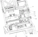
As shown in fig. 1 to 5, in one embodiment of the present application, an automatic detection apparatus for an electronic product includes:
the switching device C comprises a turnover mechanism C10 and a turnover mechanism C20, and is installed on the rack E;
the turnover mechanism C10 includes a three-dimensional motion mechanism and a supporting platform for supporting the electronic product M, and the supporting platform moves in a three-dimensional space under the driving action of the three-dimensional motion mechanism;
the turnover mechanism C20 comprises a turnover driving mechanism C22 and a clamping part C21 for clamping the electronic product M, wherein the clamping part C21 is mounted on a mounting shaft of the turnover driving mechanism C22;
and the photographing device F is arranged on the rack E, faces the switching device C and is used for photographing the electronic product M placed on the bearing platform.
In this embodiment, by configuring the switching device C and the photographing device F, the front, side, four corners, and back of the electronic product M can be photographed and identified, so as to photograph and detect the color, defect, and the like of the electronic product M, so as to classify and recycle the used electronic products M of different models, and provide a data detection basis for evaluation of the used electronic products M.
The electronic product M may be a related product based on electric energy, and includes: watches, smart phones, telephones, televisions, video disc players, video recorders, camcorders, radios, radio cassettes, combination speakers, compact disc players, computers, game consoles, mobile communication products, and the like.
As shown in fig. 1 to 5, the photographing apparatus F includes: a first area-array camera F11 mounted on the frame E. The first area-array camera F11 can acquire images at one time and can acquire images in time, the application range is wide, the area, the shape, the size and the position are measured, even the temperature is measured, the first area-array camera F11 can acquire two-dimensional image information quickly and accurately, and very visual measurement images are provided.
Further, the photographing device F further includes: a camera bellows light source F12, the camera bellows light source F12 arranged on the frame E is matched with the first area array camera F11. The camera bellows light source F12 provides light source for the first area-array camera F11 to obtain better photographing effect.
In the present embodiment, the dark box light source F12 has a plurality of light emitting surfaces, and each light emitting surface is a matte surface structure. The matte surface structure has a diffuse reflection surface, and can reduce reflection and the like.
In this embodiment, the camera bellows light source F12 preferably has four light emitting surfaces, and a circumferential light source can be provided to provide a light source for the operation of the first area-array camera F11, so as to obtain better photographing effect. The light source F12 of the camera bellows is suitable for providing 360 degrees, such as five light emitting surfaces, six light emitting surfaces, or even more light emitting surfaces arranged along the circumference. The specific number of the light emitting surfaces is only for illustration and is not intended to limit the scope of the present application.
For convenience of manufacture and installation, in this embodiment, the light box F12 is preferably a one-piece integrated light source.
Further preferably, the photographing device F further includes: a second area-array camera F21 mounted on the frame E. The second area array camera F21 can once only acquire images and can in time carry out image acquisition, and the range of application is wider, for example area, shape, size, position, even measurement such as temperature, second area array camera F21 can be fast accurate acquire two-dimensional image information, has very audio-visual measurement image moreover.
In this embodiment, the second area-array camera F21 is used to photograph some special defects of the electronic product M, and is used to make up for the defects that other cameras cannot cover, preferably, the second area-array camera F21 may be used to photograph the front side of the electronic product M, and further preferably, the second area-array camera F21 may be used to photograph the back side of the electronic product M.
The photographing device F further includes: an area array light source F22, the area array light source F22 is installed on the frame E, and the area array light source F22 is matched with the second area array camera F21. The area array light source F22 provides a light source for the operation of the second area array camera F21, so as to obtain better photographing effect.
In order to detect the appearance defects of the electronic product M more fully, the present embodiment is configured with the first line-scan camera F31 and the second line-scan camera F41 described below in addition to the first area-scan camera F11 and the second area-scan camera F21 described above. The line scan camera is a special industrial camera, only has one line of photosensitive elements, can be used for high-speed scanning and high resolution, is applied to the field of continuous detection, such as metal, plastic, paper, fiber and the like, and can process pictures one line by one line or form a plurality of pictures for processing so as to achieve uniform detection of the whole surface of the pictures.
Specifically, the photographing device F includes: a first line-scan camera F31, the first line-scan camera F31 being mounted on the chassis E.
The photographing device F further includes: a first line scan light source F32 mounted on the frame E, the first line scan light source F32 being disposed between the first line scan camera F31 and the switching device C. The first line scan light source F32 provides a light source for the operation of the first line scan camera F31 to obtain better photographing effect. The position of the first line scan light source F32 is not limited to the position shown in fig. 2, and it is preferable that the first line scan camera F31 be provided with a light source.
Further, the photographing device F includes: a second line-scan camera F41, the second line-scan camera F41 also being mounted on the chassis E.
The photographing device F further includes: a second line-scan light source F42 mounted on the chassis E, the second line-scan light source F42 being disposed between the second line-scan camera F41 and the switching device C. As described above, the second line scan light source F42 provides a light source for the operation of the second line scan camera F41 to obtain better photographing effect. The position of the second line-scan light source F42 is not limited to the position shown in fig. 2, and it is preferable that the second line-scan camera F41 be provided with a light source.
In order to obtain a better photographing effect, the present embodiment is further configured with a photographing light source G, the photographing light source G is installed on the rack E, and the photographing light source G is preferably disposed below the switching device C to provide a light source support for photographing in the process of turning over the electronic product.
As shown in fig. 23, the present application further provides an automatic detection method for an electronic product M, which includes the following steps:
step one, photographing and identifying the front side of the electronic product M;
step two, photographing and identifying the side surface of the electronic product M;
step three, photographing and identifying four corners of the electronic product M;
and step four, photographing and identifying the back of the electronic product M.
In the embodiment, the front, side, four corners and the back of the electronic product M are photographed and identified to perform photographing detection on the color, defects and the like of the electronic product M, so that the different models of used electronic products M are classified and recycled, and a data detection basis is provided for evaluation of the used electronic products M and the like.
The above-mentioned automatic detection device for the electronic product M and the specific technical solution thereof are described in detail above, and are not described herein again.
Wherein, in the step one, the method comprises the following steps: based on the first area-array camera F11, a first photo is taken of the front side of the electronic product M placed on the switching device C for identifying the external contour of the electronic product M, and the photographing light source disposed below the electronic product M is in an on state at this time.
Specifically, the first area-array camera F11 detects the contour, such as size, position, etc., of the electronic product M and transmits the detected contour to the control system, so as to provide a coordinate basis for subsequent operations, such as turning and flipping.
In the first step, the method further includes: and turning off the photographing light source and turning on a camera bellows light source F12, wherein the first area-array camera F11 continues to photograph at least two front sides of the electronic product M to prepare for the next effective photograph.
Specifically, the above-mentioned photographing process is preferably a blind photograph, wherein the number of photographs is preferably 5, so as to provide a parameter basis for the next effective photograph, and the like.
The photo taking effect can be better obtained by controlling the on-off of the light sources, such as closing the photo taking light source and opening the camera bellows light source F12, and the photo after photo taking is transmitted to the control system for storage, analysis, detection, signal output and the like.
After the parameter basis is obtained, in the above photographing and identifying the front side of the electronic product M, the method further includes: the first area-array camera F11 takes a picture of the front surface of the electronic product M to identify the color of the front surface of the electronic product M and whether the front surface is defective.
After the front detection of the electronic product M is completed, the side surface and four corners of the electronic product M need to be subjected to appearance detection.
Specifically, in the step of recognizing the side of the electronic product M by taking a picture, the method includes: by controlling the turnover mechanism C10, the side of the electronic product M is sequentially disposed toward the first area camera F11, and the first area camera F11 sequentially identifies the color of each side of the electronic product M and whether there is a defect. The control of the turnover mechanism C10 is described above and will not be described in detail here.
Specifically, in the recognition of taking a picture of the four corners of the electronic product M, the following steps are included: by controlling the turnover mechanism C10, four corners of the electronic product M are sequentially set toward the first area camera F11, and the first area camera F11 sequentially identifies the color of each corner of the electronic product M and whether there is a defect.
In order to improve the accuracy of detection, it is also necessary to adopt a strengthened detection means, specifically, by configuring the first and second line scan cameras F31 and F41.
The electronic product M is restored to be arranged with the front side facing upwards by controlling the turnover mechanism C10, and the electronic product M is driven to move linearly under the driving action of the three-dimensional movement mechanism, and in the process of the linear movement, the first linear scanning camera F31 and the second linear scanning camera F41 sequentially scan the front side of the electronic product M and obtain two front side photos of the electronic product M. This step is mainly used to detect whether the front side of the electronic product M has defects, such as cracks.
Of course, in practical applications, since the crack has directionality, it is necessary to change multiple angles to complete the detection. One preferred way is: the electronic product M is rotated by 90 degrees by controlling the turnover mechanism C10, the electronic product M is driven to linearly move under the driving action of the three-dimensional movement mechanism, and in the linear movement process, the first linear scanning camera F31 and the second linear scanning camera F41 sequentially scan the front of the electronic product M and obtain two front photos of the electronic product M.
Further, the rotation angle may be 0 to 90 °, and multiple line scan photographing detections may be performed for different rotation angles.
After the front side of the electronic product M is photographed and detected by the first and second line-scan cameras F31 and F41, the side of the electronic product M needs to be photographed and detected.
Specifically, by controlling the turnover mechanism C10, the side of the electronic product M is sequentially disposed toward the first line-scan camera F31 and the second line-scan camera F41, and the electronic product M is driven to perform linear motion under the driving action of the three-dimensional motion mechanism, during the linear motion, the first line-scan camera F31 and the second line-scan camera F41 sequentially scan each side of the electronic product M and obtain a side photograph of the corresponding electronic product M.
Preferably, the process of flapping sides described above generally requires only one single linear motion.
So far, the front side of the electronic product M is photographed and detected, and the back side of the electronic product M is detected.
Specifically, in the step four, the photographing recognition of the back side of the electronic product M includes: by controlling the turnover mechanism C10 and the turnover mechanism C20, the electronic product M is transferred from the turnover mechanism C10 to the turnover mechanism C20, and is turned over under the driving action of the turnover mechanism C20, and then the turnover mechanism C10 transfers the electronic product M after being turned over to the supporting platform.
The specific matching process of the turnover mechanism C10 and the turnover mechanism C20 is described above.
And after the electronic product M finishes turning over, photographing and detecting the appearance of the back of the electronic product M.
Specifically, the electronic product M is driven to move linearly by the driving action of the three-dimensional movement mechanism, and during the linear movement, the first line-scan camera F31 and the second line-scan camera F41 sequentially scan the back of the electronic product M and obtain two back photos of the electronic product M.
As described above, since cracks and the like have directionality, it is necessary to change a plurality of angles to complete detection. One preferred way is: the electronic product M is rotated by 90 degrees by controlling the turnover mechanism C10, the electronic product M is driven to linearly move under the driving action of the three-dimensional movement mechanism, and in the linear movement process, the first linear scanning camera F31 and the second linear scanning camera F41 sequentially scan the back of the electronic product M and obtain two back photos of the electronic product M.
Further, the rotation angle may be 0 to 90 °, and multiple line scan photographing detections may be performed for different rotation angles.
In the above-mentioned recognition of taking a picture of the back of the electronic product M, the method further includes: based on the first area-array camera F11, a first photograph is taken of the back side of the electronic product M placed on the switching device C. Specifically, the second area-array camera F21 detects the contour, such as size and position, of the electronic product M and transmits the detected contour to the control system, so as to provide a coordinate basis for subsequent operations, such as turning and flipping.
In the above-mentioned recognition of taking a picture of the back of the electronic product M, the method further includes: at least two electronic products M placed on the switching device C are blindly photographed on the back side based on the first area-array camera F11 to prepare parameters for the next valid photograph.
Specifically, the above-mentioned photographing process is preferably a blind photograph, wherein the number of photographs is preferably 5, so as to provide a parameter basis for the next effective photograph, and the like.
After the parameter basis is obtained, in the above photographing and identifying the back of the electronic product M, the method further includes: based on the first area-array camera F11, another photo is taken of the back side of the electronic product M placed on the switching device C to identify the color of the back side of the electronic product M and whether the back side is defective.
In the above-mentioned recognition of taking a picture of the back of the electronic product M, the method further includes: based on the second area-array camera F21 and the area-array light source F22, each sub-light source of the area-array light source F22 is turned on in sequence, and the second area-array camera F21 takes multiple photographs of the back of the electronic product M in sequence.
In the present embodiment, the area array light source F22 is preferably a low-angle bar light source.
In the above-mentioned recognition of taking a picture of the back of the electronic product M, the method further includes: all the sub-light sources of the area array light source F22 are turned on, and the second area array camera F21 takes a picture of the back of the electronic product M.
Through the setting of the photographing step of the second area-array camera F21, the special defects of the electronic product M can be photographed, and due to the fact that the back of the electronic product M is made of a plurality of materials, the second area-array camera F21 can make up the defects that other cameras cannot cover the electronic product M.
After the back side photographing detection of the electronic product M is completed, the electronic product M is transferred to the clamping device a through the turnover mechanism C10, and the transfer process of the turnover mechanism C10 and the clamping device a about the electronic product M is described above, and is not described here again.
After the electronic product M is clamped by the clamping device a, the worker can take out the detected electronic product M to perform appearance detection of the next electronic product M, and the like.
As shown in fig. 6 to 10, the present embodiment further includes a clamping mechanism a for adjusting the electronic products, and the clamping mechanism a is mounted on the rack E. Through the placing opening formed in the frame E, the electronic product can be placed on the clamping mechanism A to prepare for photographing detection and the like.
The clamping device a includes: the base A10, the base A10 has a placing plane, the placing plane is used for placing the electronic product M;
a first clamping jaw A20 and a second clamping jaw A22, wherein the first clamping jaw A20 and the second clamping jaw A22 are respectively arranged at two sides of the base A10, and the first clamping jaw A20 and the second clamping jaw A22 are matched with each other to clamp or release the electronic product M;
clamping actuating mechanism A30, be equipped with first slider A31 and second slider A32 on clamping actuating mechanism A30 under clamping actuating mechanism A30's drive effect, first slider A31 with second slider A32 moves in opposite directions or carried on the back, install respectively on first slider A31 with second slider A32 first clamping jaw A20 with second clamping jaw A22.
In this embodiment, by providing the first clamping jaw a20, the second clamping jaw a22 and the clamping driving mechanism a30, the position of the electronic product M to be detected can be sorted, the structure is simple, the control mode is easy to control, the accuracy is high, the center lines of the electronic products M of different types and different denominations can be always located at the same position, and a detection reference is provided for subsequent further detection.
Further, the clamping driving mechanism a30 may be a parallel cylinder, wherein the first slider a31 and the second slider a32 are two sliders disposed on the parallel cylinder.
Further, in order to ensure the consistency of the movement of the two sliders, in the embodiment, two separate driving assemblies may be provided, and the performance structures and the like of the driving assemblies are set to be the same, and under the control of the same control unit, the first slider a31 and the second slider a32 are controlled to move in the same direction or in a reverse direction, so as to complete the operation of clamping or releasing the electronic product M.
Due to the consistency of the movement of the first slider A31 and the second slider A32, the movement of the first clamping jaw A20 and the movement of the second clamping jaw A22 which are installed on the first slider A31 and the second slider A32 are synchronized, so that the central lines of electronic products M of different models are always in the same position.
In the present embodiment, a sensor a40 (shown in fig. 3) for detecting the electronic product M is further included, and the sensor a40 is disposed near the upper side of the placement plane. The sensor a40 is used for detecting whether an electronic product M is placed on the base a 10.
Preferably, when the electronic product M is placed, it is preferably arranged to be attached to the control surface of the sensor, so that the relative position of the electronic product M is easily defined.
Further, to complete the installation of the sensor a40, the present embodiment further includes a mounting assembly a41, and the sensor a40 is mounted on the rack E through the mounting assembly a 41. Preferably, the mounting assembly a41 is disposed to semi-wrap the sensor a40, so as to protect the sensor a40 and prevent the sensor a40 from being damaged due to accidents and the like while ensuring the mounting.
The number of the sensors a40 is at least two, and the arrangement of the plurality of sensors a40 can prevent the placing position of the electronic product M from deviating too much, thereby reducing the driving adjustment range of the clamping driving mechanism a30 and the like; in addition, if one sensor A40 breaks down, the other sensors A40 can still work continuously, and the operation progress of the whole machine is not affected.
In this embodiment, be equipped with first clamping face on the first clamping jaw a20, be equipped with second clamping face on the second clamping jaw a22, first clamping face with second clamping face is in opposite directions and mutual parallel arrangement. Under the general condition, electronic product M is mostly the rectangle mechanism, through the setting of above-mentioned first clamping face and second clamping face, can guarantee clamping stability and reliability.
Furthermore, in order to reduce the rigid damage and the like to the electronic product M in the clamping process, a buffer layer structure is arranged on the first clamping surface/the second clamping surface.
The buffer layer structure is preferably made of a flexible material or an elastic material, such as rubber, and the buffer layer structure may be fixed on the first clamping surface or the second clamping surface by means of adhesion or the like.
Of course, in the present embodiment, the first clamping jaw a20 and the second clamping jaw a22 are made of flexible material or elastic material, such as rubber. In other words, in a specific implementation, the first clamping jaw a20 and the second clamping jaw a22 may be supported by a flexible material or an elastic material, so as to reduce the installation manner of the buffer layer structure, which is needed, and facilitate the realization of a batch operation manner such as integrated processing.
Preferably, the bottom surface of the first clamping jaw a 20/the second clamping jaw a22 is higher than the upper surface of the base a10 and lower than the top surface for placing the electronic product M. That is, with the above arrangement, in each clamping process, it is necessary to always ensure that the first clamping jaw a20 and the second clamping jaw a22 can complete clamping of the electronic product M, and thus, occurrence of ineffective work such as empty clamping is avoided.
Of course, in the specific embodiment, the bottom surfaces of the first clamping jaw a20 and the second clamping jaw a22 are arranged on the same horizontal plane or on different horizontal planes. When the clamping device is arranged on the same horizontal plane, the clamping operation is more stable and reliable.
Further, as shown in fig. 6 to 10, the first jaw a20 is connected to the first slider a31 by a first bending member a21, and the second jaw a22 is connected to the second slider a32 by a second bending member a 23. Of course, the first jaw a20 and the first bending member a21 may be provided as an integrally formed structure, and the second jaw a22 and the second bending member a23 may be provided as an integrally formed structure; the number of parts used is reduced, the complexity of installation is reduced, and batch processing operation is facilitated.
Further, in order to improve the detection accuracy, as shown in fig. 11 to 15, the present embodiment is further provided with a first dust removing device B which is disposed above the holding device a and applies the high-pressure gas with ions blown out to the electronic product M, and the first dust removing device B includes: a first ionizer B1 and a first air supply delivery passage provided in communication with the first ionizer B1.
Further, the first dust removing device B further includes a first air knife (not shown), and the first air knife is disposed near the outlet of the first ionizer B1. After passing through the first air knife, the high-pressure air is blown out at high speed by an airflow sheet with the thickness of only 0.05 mm, so that a thin impact air curtain with high strength and large airflow can be formed, and dust and the like on the surface of the electronic product M can be blown off to achieve the aim of cleaning. Specifically, the thin sheet air curtain can be 30-40 times of the maximum ambient air through the principle of the coanda effect and the special geometric shape of the air knife, so that the thin impact air curtain with high strength and large airflow is formed.
The first air knife is made of aluminum alloy or stainless steel, the aluminum alloy air knife is subjected to electroplating treatment in the manufacturing process, the service life of the air knife is far longer than that of other similar products, and the stainless steel air knife can be used in high-temperature and high-corrosion environments.
Further, as shown in fig. 14, the first dust removing device B further includes at least one first dust collecting cover B2 for collecting dust, and the first dust collecting cover B2 is disposed at a side of the holding device a. In this embodiment, the first dust collection cover B2 is preferably provided in two pieces, and each of the two pieces is provided on a side surface of the holder a, and more preferably, an upper surface of the first dust collection cover B2 is provided lower than a placement plane of the holder a, so that dust and the like removed by the first dust removal device B flies down or is sucked into the first dust collection cover B2 by a negative pressure suction device described below.
In the present embodiment, the first dust collecting cover B2 is preferably a hopper-shaped structure having a large top size and a small bottom size, so as to facilitate dust collection to the bottom, etc.
In particular, in order to better collect dust and the like on the surface of the electronic product M, a first side surface of the first dust hood B2, which is away from the clamping device a, is slightly higher than a second side surface of the first dust hood B2, which is close to the clamping device a. The arrangement can lead part of dust removed by the first dust removing device B to be intercepted by the first side surface and fall into the first dust collecting cover B2, thereby collecting the dust and the like to the maximum extent for centralized processing and the like.
For convenience of processing, the first side surface and the second side surface of the first dust cage B2 may be formed to have the same height.
The first dust collecting cover B2 is further provided with a first negative pressure suction device, and dust and the like can be better collected in the first dust collecting cover B2 by the arrangement of the first negative pressure suction device.
Further, in order to ensure the integrity of the dust removing operation, the present embodiment is further configured with a second dust removing device D, which is disposed above the switching device C and blows out a high-pressure gas with ions to act on the electronic product M, wherein the second dust removing device D includes: a second ion generator D1 and a second air supply delivery channel, wherein the second air supply delivery channel is communicated with the second ion generator D1. In the same way as the first dust removing device B, the second dust removing device D further includes a second air knife, and the second air knife is disposed near the outlet of the second ion generator D1. After passing through the second air knife, the high-pressure air is blown out at high speed by the airflow sheet with the thickness of only 0.05 mm, so that a thin impact air curtain with high strength and large airflow can be formed, and dust and the like on the surface of the electronic product M can be blown off to achieve the aim of cleaning. Specifically, the thin sheet air curtain can be 30-40 times of the maximum ambient air through the principle of the coanda effect and the special geometric shape of the air knife, so that the thin impact air curtain with high strength and large airflow is formed.
Further, as shown in fig. 15, the second dust removing device D further includes at least one second dust collection cover D2 for collecting dust, and the second dust collection cover D2 is disposed at a side of the switching device C. In this embodiment, it is preferable that the second dust collection covers D2 are provided in two numbers, and are respectively provided on the side surfaces of the holder a.
Since the second dust removing device D is disposed in cooperation with the switching device C and the position of the electronic product M is not unique during the movement of the switching device C, the second dust collecting cover D2 is preferably disposed toward the switching device C, i.e., in a manner of being disposed as shown in fig. 11 and 15, so that the collected dust and the like can be more greatly scattered after being removed by the second dust removing device D or absorbed in the second dust collecting cover D2 by a second negative pressure suction device described below.
In this embodiment, the second dust collecting cover D2 is preferably a hopper-shaped structure having a large opening and a small collecting part, so as to collect dust into the collecting part.
In a specific implementation, in order to better collect dust and the like on the surface of the electronic product M, the first side surface of the second dust collecting cover D2, which is disposed near the lower portion of the switching device C, is disposed beyond the second side surface of the second dust collecting cover D2, which is disposed near the upper portion of the switching device C, so that a part of the dust removed by the second dust removing device D is intercepted by the first side surface disposed below and falls into the second dust collecting cover D2, thereby collecting the dust and the like to the maximum extent for centralized processing and the like.
In the dust removing apparatus for inspecting the electronic product M, the second dust collecting cover D2 is further provided with a second negative pressure suction device, and the second negative pressure suction device is provided to better collect dust and the like in the second dust collecting cover D2.
This embodiment can make the outside of electronic product M remove dust comprehensively through first dust collector B and second dust collector D's setting, blows out the high-pressure gas who takes the ion, and wherein, the ion in the high-pressure gas can neutralize the static on electronic product M surface, makes the dust reduce electrostatic adsorption and drops easily.
The first air source delivery passage or the second air source delivery passage can be also provided with a compressor and an air filter, clean air is input after filtration, and the speed of compressed air or high-pressure air can be adjusted through a regulator.
The first ionizer B1 or the second ionizer D1 mentioned above uses a high voltage transformer to boost the power frequency voltage to the required voltage to ionize the surrounding air, and ionize the air into positive ions and negative ions, these ions are adsorbed by the ions of opposite polarity to neutralize the static electricity, and the remaining ions disappear rapidly into the atmosphere.
As shown in fig. 16, in this embodiment, an air filter unit N is further provided, and the air filter unit N is mounted on the frame E. The outside air enters the rack E through the air filtering unit N, and the air filtered by the air filtering unit E is clean air.
Due to the arrangement of the air filtering unit N, the internal air pressure of the rack E is larger than the external air pressure, and clean air flows out from all gaps on the rack E, so that external dust cannot enter the rack E, and the internal cleanness of the rack E is kept.
In this embodiment, as shown in fig. 17 to 20, the flipping mechanism C10 includes a three-dimensional motion mechanism and a supporting platform for supporting the electronic product M, and the supporting platform moves in a three-dimensional space under the driving action of the three-dimensional motion mechanism;
the turnover mechanism C20, the turnover mechanism C20 includes a turnover driving mechanism C22 and a clamping part C21 for clamping the electronic product M, the clamping part C21 is mounted on the mounting shaft of the turnover driving mechanism C22;
when the flipping mechanism C10 is disposed close to the flipping mechanism C20, the clamping portion C21 clamps the electronic product M and drives the clamping portion C21 to flip 180 ° under the driving action of the flipping driving mechanism C22.
In this embodiment, by providing the flipping mechanism C20, the electronic product M placed on the supporting platform can be turned 180 ° after being clamped by the flipping mechanism C20, so as to realize the flipping process of the electronic product M, for example, the electronic product M with the front side facing upward is flipped so that the back side faces upward, or the electronic product M with the back side facing upward is flipped so that the front side faces upward.
The clamping portion C21 is preferably made of a flexible or elastic material, such as rubber, which can reduce the clamping damage to the electronic product M during the clamping process.
Preferably, a buffer layer is adhered or fixed on the clamping surface of the clamping portion C21 by other conventional fixing means, and the buffer layer is preferably made of flexible or elastic material, such as rubber, etc., so as to reduce the clamping damage to the electronic product M during the clamping process.
Further, as shown in fig. 20 to 22, the holding platform includes a holding portion C12 and an RO shaft driving mechanism C11 for driving the holding portion C12 to turn, and the RO shaft driving mechanism C11 is installed on the three-dimensional moving mechanism. The bearing part C12 can rotate by C360 ° along the plane of the bearing part C12 under the driving operation of the RO shaft driving mechanism C11, so as to cooperate with the electronic product M recycling mechanism to completely detect each angle or side of the electronic product M.
At least one suction cup C121 is disposed on the supporting portion C12, the suction cup C121 is further communicated with a negative pressure mechanism, and the suction cup C121 is used for adsorbing the electronic product M. The electronic product M can be firmly adsorbed on the supporting part C12 by the negative pressure mechanism, when the electronic product M on the supporting part C12 needs to be transferred to the clamping part C21 in the turn-over mechanism C20, the control system can control the negative pressure mechanism to reduce the suction pressure or close the negative pressure mechanism, and the electronic product M is clamped by matching with the clamping part C21, so that the electronic product M is transferred from the turn-over mechanism C10 to the turn-over mechanism C20, and finally the turn-over operation of the electronic product M is realized.
Furthermore, one or more limiting columns C122 with a height corresponding to that of the suction cup C121 are arranged on the supporting portion C12. The supporting part C12 is provided with limiting columns C122, so that the electronic product M to be detected is at a preset horizontal plane, wherein the number of the limiting columns C122 is adaptively set according to the size of the supporting part C12, and the number of the limiting columns C122 can be one, two, four, six or more. When the limiting columns C122 are provided with a plurality of columns, the rotation centers of the bearing parts C12 are used as symmetry centers, and the columns are symmetrically arranged left and right and front and back; the height of the limiting column C122 and the height of the sucker C121 are adaptively arranged, and when the sucker C121 does not suck the electronic product M, the sucking end of the sucker C121 is slightly higher than the limiting column C122; when the suction cup C121 adsorbs the electronic product M, the adsorption end of the suction cup C121 contracts under the action of negative pressure, so that the height of the adsorption end is slightly lower than that of the limiting column C122, and in the contraction process, the suction cup C121 drives the adsorbed surface of the electronic product M to press against the limiting column C122, so that the electronic product M to be detected is located on a preset plane.
As shown in fig. 19, the present embodiment is also provided with a rotary drive mechanism C60, the rotary drive mechanism C60 including: a rotary driving motor C61, a first gear C62 and a second gear C63, wherein the first gear C62 and the second gear C63 are in transmission connection through a first synchronous belt (not shown in the figure), the first gear C62 is installed on a driving shaft of the rotary driving motor C61, and the second gear C63 is fixedly connected with a mounting shell C13 of the supporting platform through a shaft; under the driving action of the rotating driving motor C61, the supporting platform performs 360-degree rotating operation. The rotation driving mechanism C60 allows the support platform to rotate 360 ° in the XOZ plane, and the RO axis driving mechanism C11 can completely detect the angles and sides of the electronic product M, thereby recycling the electronic product M.
In the present embodiment, the rotary drive mechanism C60 is mounted on a Z-axis drive mechanism described below, and specifically, the mounting bracket of the rotary drive mechanism C60 is mounted on the Z-axis slider.
The three-dimensional motion mechanism comprises an X-axis motion mechanism C40, a Y-axis motion mechanism C30 and a Z-axis motion mechanism C50, the X-axis motion mechanism C40 is connected with the Y-axis motion mechanism C30 in a sliding mode, the Z-axis motion mechanism C50 is connected with the X-axis motion mechanism C40 in a sliding mode, the Y-axis motion mechanism C30 is installed on the rack E, and the Z-axis motion mechanism C50 is further provided with the bearing platform. Through the arrangement of the three-dimensional movement mechanism, the supporting platform supporting the electronic product M can move in a three-dimensional space (X-axis, Y-axis and Z-axis directions).
Under the action of the three-dimensional movement mechanism, the rotary driving mechanism C60 and the RO shaft driving mechanism C11, the electronic product M on the supporting part C12 can be detected comprehensively in multiple angles and multiple directions, and the detection comprehensive degree and accuracy are provided.
Further, Y axle motion C30 includes Y axle lead screw, Y axle slider and Y axle driving motor, Y axle driving motor with Y axle lead screw is connected and drives Y axle lead screw rotates, Y axle slider with Y axle lead screw threaded connection, still install on the Y axle slider X axle motion C40, Y axle driving motor installs on the frame E. When the Y-axis driving motor works, the X-axis motion mechanism C40 arranged on the Y-axis slide block can be driven to do linear reciprocating motion along the Y direction.
Further, X axle motion C40 includes X axle lead screw, X axle slider and X axle driving motor, X axle driving motor with the X axle lead screw is connected and is driven the X axle lead screw rotates, X axle slider with X axle lead screw threaded connection, still install on the X axle slider Z axle motion C50. When the X-axis driving motor works, the Z-axis motion mechanism C50 arranged on the X-axis slide block can be driven to do linear reciprocating motion along the X direction.
Further, Z axle motion C50 includes Z axle lead screw, Z axle slider and Z axle driving motor C51, Z axle driving motor C51 with the Z axle lead screw is connected and drives the Z axle lead screw rotates, Z axle slider with Z axle lead screw threaded connection, still install on the Z axle slider the bearing platform. When the Z-axis driving motor C51 works, the supporting platform arranged on the Z-axis sliding block can be driven to do linear reciprocating motion along the Z direction.
Further, in order to improve the driving stability of the Z-axis driving motor C51, the output end of the Z-axis driving motor C51 is further provided with a third gear C52, the Z-axis lead screw is further provided with a fourth gear C53, and the third gear C52 and the fourth gear C53 are engaged through a second synchronous belt (not shown in the figure) to realize synchronous transmission.
In the description of the present application, unless expressly stated or limited otherwise, the terms "connected," "connected," and "fixed" are to be construed broadly, e.g., as meaning permanently connected, removably connected, or integral to one another; can be mechanically or electrically connected; either directly or indirectly through intervening media, either internally or in any other relationship. The specific meaning of the above terms in the present application can be understood in a specific case by those of ordinary skill in the art.
In this application, unless expressly stated or limited otherwise, the first feature "on" or "under" the second feature may comprise direct contact of the first and second features, or may comprise contact of the first and second features not directly but through another feature in between. Also, the first feature being "on," "above" and "over" the second feature includes the first feature being directly on and obliquely above the second feature, or merely indicating that the first feature is at a higher level than the second feature. A first feature being "under," "below," and "beneath" a second feature includes the first feature being directly under and obliquely below the second feature, or simply meaning that the first feature is at a lesser elevation than the second feature.
In the description of the present embodiment, the terms "upper", "lower", "right", etc. are used in an orientation or positional relationship based on that shown in the drawings only for convenience of description and simplicity of operation, and do not indicate or imply that the device or element referred to must have a particular orientation, be constructed and operated in a particular orientation, and thus should not be construed as limiting the present application. Furthermore, the terms "first" and "second" are used only for descriptive purposes and are not intended to have a special meaning.
The above embodiments are merely to illustrate the technical solutions of the present application and are not limitative, and the present application is described in detail with reference to preferred embodiments. It will be understood by those skilled in the art that various modifications and equivalent arrangements may be made in the present invention without departing from the spirit and scope of the present invention and shall be covered by the appended claims.