CN112631523A - Selection method for solid state disk garbage recovery victim block - Google Patents
Selection method for solid state disk garbage recovery victim block Download PDFInfo
- Publication number
- CN112631523A CN112631523A CN202011601090.1A CN202011601090A CN112631523A CN 112631523 A CN112631523 A CN 112631523A CN 202011601090 A CN202011601090 A CN 202011601090A CN 112631523 A CN112631523 A CN 112631523A
- Authority
- CN
- China
- Prior art keywords
- block
- solid state
- garbage collection
- state disk
- blocks
- Prior art date
- Legal status (The legal status is an assumption and is not a legal conclusion. Google has not performed a legal analysis and makes no representation as to the accuracy of the status listed.)
- Granted
Links
Images


Classifications
-
- G—PHYSICS
- G06—COMPUTING OR CALCULATING; COUNTING
- G06F—ELECTRIC DIGITAL DATA PROCESSING
- G06F3/00—Input arrangements for transferring data to be processed into a form capable of being handled by the computer; Output arrangements for transferring data from processing unit to output unit, e.g. interface arrangements
- G06F3/06—Digital input from, or digital output to, record carriers, e.g. RAID, emulated record carriers or networked record carriers
- G06F3/0601—Interfaces specially adapted for storage systems
- G06F3/0628—Interfaces specially adapted for storage systems making use of a particular technique
- G06F3/0646—Horizontal data movement in storage systems, i.e. moving data in between storage devices or systems
- G06F3/0652—Erasing, e.g. deleting, data cleaning, moving of data to a wastebasket
-
- G—PHYSICS
- G06—COMPUTING OR CALCULATING; COUNTING
- G06F—ELECTRIC DIGITAL DATA PROCESSING
- G06F3/00—Input arrangements for transferring data to be processed into a form capable of being handled by the computer; Output arrangements for transferring data from processing unit to output unit, e.g. interface arrangements
- G06F3/06—Digital input from, or digital output to, record carriers, e.g. RAID, emulated record carriers or networked record carriers
- G06F3/0601—Interfaces specially adapted for storage systems
- G06F3/0602—Interfaces specially adapted for storage systems specifically adapted to achieve a particular effect
- G06F3/0614—Improving the reliability of storage systems
- G06F3/0616—Improving the reliability of storage systems in relation to life time, e.g. increasing Mean Time Between Failures [MTBF]
-
- G—PHYSICS
- G06—COMPUTING OR CALCULATING; COUNTING
- G06F—ELECTRIC DIGITAL DATA PROCESSING
- G06F3/00—Input arrangements for transferring data to be processed into a form capable of being handled by the computer; Output arrangements for transferring data from processing unit to output unit, e.g. interface arrangements
- G06F3/06—Digital input from, or digital output to, record carriers, e.g. RAID, emulated record carriers or networked record carriers
- G06F3/0601—Interfaces specially adapted for storage systems
- G06F3/0628—Interfaces specially adapted for storage systems making use of a particular technique
- G06F3/0638—Organizing or formatting or addressing of data
- G06F3/064—Management of blocks
-
- G—PHYSICS
- G06—COMPUTING OR CALCULATING; COUNTING
- G06F—ELECTRIC DIGITAL DATA PROCESSING
- G06F3/00—Input arrangements for transferring data to be processed into a form capable of being handled by the computer; Output arrangements for transferring data from processing unit to output unit, e.g. interface arrangements
- G06F3/06—Digital input from, or digital output to, record carriers, e.g. RAID, emulated record carriers or networked record carriers
- G06F3/0601—Interfaces specially adapted for storage systems
- G06F3/0668—Interfaces specially adapted for storage systems adopting a particular infrastructure
- G06F3/0671—In-line storage system
- G06F3/0673—Single storage device
- G06F3/0679—Non-volatile semiconductor memory device, e.g. flash memory, one time programmable memory [OTP]
Landscapes
- Engineering & Computer Science (AREA)
- Theoretical Computer Science (AREA)
- Human Computer Interaction (AREA)
- Physics & Mathematics (AREA)
- General Engineering & Computer Science (AREA)
- General Physics & Mathematics (AREA)
- Techniques For Improving Reliability Of Storages (AREA)
- Information Retrieval, Db Structures And Fs Structures Therefor (AREA)
Abstract
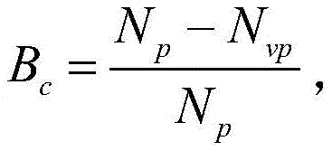
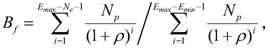
本发明属于计算机存储系统设计技术领域,具体涉及用于固态硬盘垃圾回收受害块的选择方法。包括如下步骤:S1,在固态硬盘SSD触发垃圾回收后,遍历所有块,计算每个块的收益B;S2,在所有块的收益B计算完成后,挑选收益B最大的块作为回收块。本发明能够通过将闪存块的未来可写入量折算到现在,避免了擦除次数较少的块因无效页较少不会被选择成VB的弊端;本发明具有能够保证在进行垃圾回收的VB选择时,考虑闪存块的磨损均衡,实现垃圾回收和磨损均衡的相统一,从而提升SSD性能和寿命的特点。
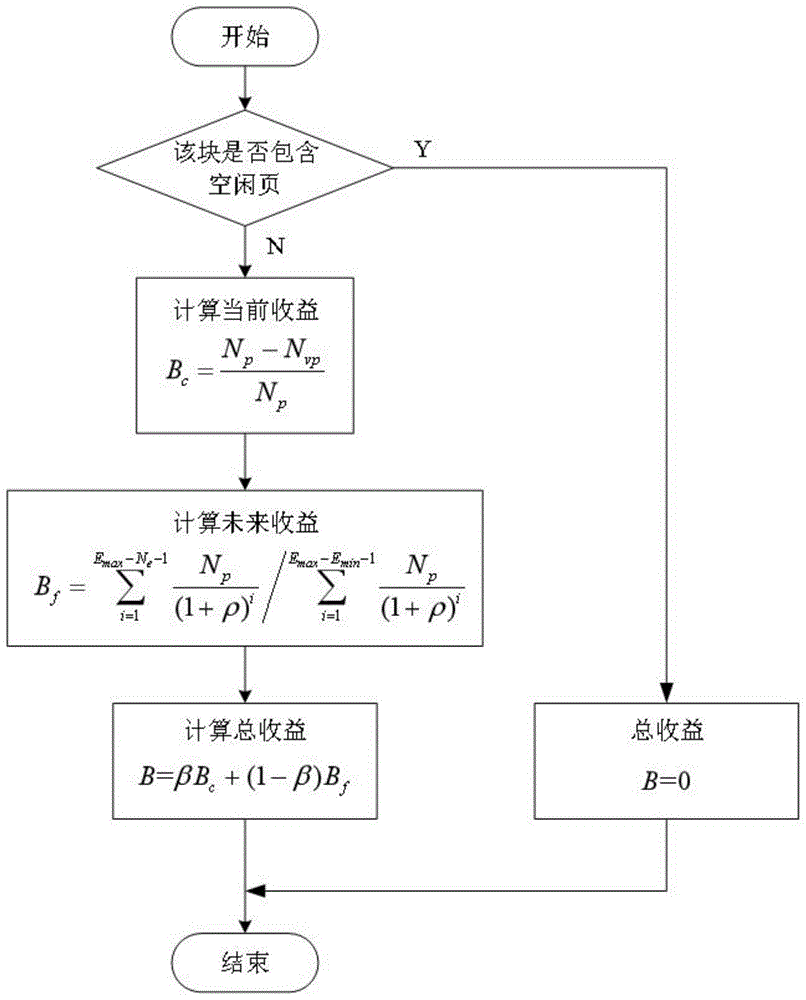
The invention belongs to the technical field of computer storage system design, and in particular relates to a method for selecting victim blocks for garbage collection of solid-state hard disks. It includes the following steps: S1, after the solid-state drive SSD triggers garbage collection, traverse all blocks and calculate the revenue B of each block; S2, after the calculation of the revenue B of all blocks is completed, select the block with the largest revenue B as the recycling block. The invention can convert the future writable amount of the flash memory block to the present, so as to avoid the disadvantage that the block with less erasing times will not be selected as VB due to less invalid pages; When selecting VB, consider the wear leveling of flash memory blocks to achieve the unification of garbage collection and wear leveling, thereby improving the performance and life of SSD.
Description


Claims (6)
Priority Applications (1)
| Application Number | Priority Date | Filing Date | Title |
|---|---|---|---|
| CN202011601090.1A CN112631523B (en) | 2020-12-29 | 2020-12-29 | Selection method for solid state disk garbage recovery victim block |
Applications Claiming Priority (1)
| Application Number | Priority Date | Filing Date | Title |
|---|---|---|---|
| CN202011601090.1A CN112631523B (en) | 2020-12-29 | 2020-12-29 | Selection method for solid state disk garbage recovery victim block |
Publications (2)
| Publication Number | Publication Date |
|---|---|
| CN112631523A true CN112631523A (en) | 2021-04-09 |
| CN112631523B CN112631523B (en) | 2022-08-30 |
Family
ID=75286349
Family Applications (1)
| Application Number | Title | Priority Date | Filing Date |
|---|---|---|---|
| CN202011601090.1A Active CN112631523B (en) | 2020-12-29 | 2020-12-29 | Selection method for solid state disk garbage recovery victim block |
Country Status (1)
| Country | Link |
|---|---|
| CN (1) | CN112631523B (en) |
Cited By (1)
| Publication number | Priority date | Publication date | Assignee | Title |
|---|---|---|---|---|
| CN119311200A (en) * | 2023-07-13 | 2025-01-14 | 四川大学 | A NAND flash memory garbage collection method based on page sequence number and update time |
Citations (4)
| Publication number | Priority date | Publication date | Assignee | Title |
|---|---|---|---|---|
| US20100325351A1 (en) * | 2009-06-12 | 2010-12-23 | Bennett Jon C R | Memory system having persistent garbage collection |
| CN108628758A (en) * | 2018-03-14 | 2018-10-09 | 深圳忆联信息系统有限公司 | A kind of method and solid state disk of selection garbage reclamation object block |
| CN111324303A (en) * | 2020-01-21 | 2020-06-23 | 深圳忆联信息系统有限公司 | SSD garbage recycling method and device, computer equipment and storage medium |
| CN111708713A (en) * | 2020-05-20 | 2020-09-25 | 杭州电子科技大学 | An intelligent garbage collection and scheduling method for solid-state drives |
-
2020
- 2020-12-29 CN CN202011601090.1A patent/CN112631523B/en active Active
Patent Citations (4)
| Publication number | Priority date | Publication date | Assignee | Title |
|---|---|---|---|---|
| US20100325351A1 (en) * | 2009-06-12 | 2010-12-23 | Bennett Jon C R | Memory system having persistent garbage collection |
| CN108628758A (en) * | 2018-03-14 | 2018-10-09 | 深圳忆联信息系统有限公司 | A kind of method and solid state disk of selection garbage reclamation object block |
| CN111324303A (en) * | 2020-01-21 | 2020-06-23 | 深圳忆联信息系统有限公司 | SSD garbage recycling method and device, computer equipment and storage medium |
| CN111708713A (en) * | 2020-05-20 | 2020-09-25 | 杭州电子科技大学 | An intelligent garbage collection and scheduling method for solid-state drives |
Non-Patent Citations (1)
| Title |
|---|
| OHHOON KWON: "FeGC: An efficient garbage collection scheme for flash memory based", 《THE JOURNAL OF SYSTEMS AND SOFTWARE》 * |
Cited By (1)
| Publication number | Priority date | Publication date | Assignee | Title |
|---|---|---|---|---|
| CN119311200A (en) * | 2023-07-13 | 2025-01-14 | 四川大学 | A NAND flash memory garbage collection method based on page sequence number and update time |
Also Published As
| Publication number | Publication date |
|---|---|
| CN112631523B (en) | 2022-08-30 |
Similar Documents
| Publication | Publication Date | Title |
|---|---|---|
| US10795586B2 (en) | System and method for optimization of global data placement to mitigate wear-out of write cache and NAND flash | |
| US8103820B2 (en) | Wear leveling method and controller using the same | |
| JP5603997B2 (en) | Storage apparatus and data control method | |
| CN107710169B (en) | Access method and device of flash memory device | |
| CN109496300B (en) | Storage medium garbage collection method, storage medium and program product | |
| CN102222046B (en) | Abrasion equilibrium method and device | |
| CN103092766B (en) | A kind of loss equalizing implementation method for NAND FLASH | |
| US20200225882A1 (en) | System and method for compaction-less key-value store for improving storage capacity, write amplification, and i/o performance | |
| US11126561B2 (en) | Method and system for organizing NAND blocks and placing data to facilitate high-throughput for random writes in a solid state drive | |
| US20190146925A1 (en) | Method and system for enhancing flash translation layer mapping flexibility for performance and lifespan improvements | |
| CN108733306B (en) | A file merging method and device | |
| KR20210099870A (en) | Memory system and operating method thereof | |
| CN103838676B (en) | Data-storage system, date storage method and PCM bridges | |
| CN110633047A (en) | Method for managing flash memory module and related flash memory controller and electronic device | |
| CN106557432B (en) | Buffer memory management method, memory control circuit unit and storage device | |
| CN112346666A (en) | Writing and block granularity compression and combination method and system of key value storage system based on OCSSD | |
| EP4012547B1 (en) | Storage method and apparatus for key value (kv) and storage device | |
| US20200327066A1 (en) | Method and system for online recovery of logical-to-physical mapping table affected by noise sources in a solid state drive | |
| CN111708713A (en) | An intelligent garbage collection and scheduling method for solid-state drives | |
| KR101480424B1 (en) | Apparatus and method for optimization for improved performance and enhanced lifetime of hybrid flash memory devices | |
| US20200133511A1 (en) | Optimized placement of data contained in a garbage collected storage system | |
| CN110347613A (en) | Method, controller and the multi-tenant solid-state disk of RAID are realized in multi-tenant solid-state disk | |
| CN116134519A (en) | Balanced three-level read disturb management in memory devices | |
| WO2017123776A1 (en) | System and method of write amplification factor mitigation and flash lifespan extension | |
| US11429519B2 (en) | System and method for facilitating reduction of latency and mitigation of write amplification in a multi-tenancy storage drive |
Legal Events
| Date | Code | Title | Description |
|---|---|---|---|
| PB01 | Publication | ||
| PB01 | Publication | ||
| SE01 | Entry into force of request for substantive examination | ||
| SE01 | Entry into force of request for substantive examination | ||
| GR01 | Patent grant | ||
| GR01 | Patent grant | ||
| TR01 | Transfer of patent right |
Effective date of registration: 20240708 Address after: 518000 1002, Building A, Zhiyun Industrial Park, No. 13, Huaxing Road, Henglang Community, Longhua District, Shenzhen, Guangdong Province Patentee after: Shenzhen Wanzhida Technology Co.,Ltd. Country or region after: China Address before: 310018 no.1158, No.2 street, Baiyang street, Hangzhou Economic and Technological Development Zone, Hangzhou, Zhejiang Province Patentee before: HANGZHOU DIANZI University Country or region before: China |
|
| TR01 | Transfer of patent right | ||
| TR01 | Transfer of patent right |
Effective date of registration: 20250416 Address after: 1034, 10th Floor, Building 27, Taihu Beili, Tongzhou District, Beijing, 100000 Patentee after: Beijing Juanpeng Interactive Entertainment Technology Co.,Ltd. Country or region after: China Address before: 518000 1002, Building A, Zhiyun Industrial Park, No. 13, Huaxing Road, Henglang Community, Longhua District, Shenzhen, Guangdong Province Patentee before: Shenzhen Wanzhida Technology Co.,Ltd. Country or region before: China |
|
| TR01 | Transfer of patent right |