Detailed Description
Repetitive Side Channel Attack (SCA) countermeasures for computing devices are described herein. The described countermeasures are suitable for preventing side-channel attacks when repeated behavior of the attack is occurring. An example of a computing device is a cryptographic engine, which may be implemented as part of a smart card.
In one scenario of a repetitive side-channel attack, the smart card applies different signals with a reset in between. Smart cards containing duplicate SCA countermeasures (or other computing devices subject to such side-channel attack scenarios) may include a timer circuit and a capacitive delay circuit that notifies of potential duplicate-based attacks by sending an activity detection signal that may be used to initiate an appropriate countermeasure response. For example, the activity detection signal may be used to reset a cryptographic engine of the smart card or perform another appropriate countermeasure response when the smart card is powered for an amount of time that is less than the amount of time for typical operation or in response to the smart card applying power or resetting within a specified amount of time after a previous application or reset of power or resetting.
In another repetitive side-channel attack scenario, the smart card is repeatedly applied with the same input signal. A smart card (or other computing device subject to such side-channel attack scenarios) containing a repetitive SCA countermeasure may include at least one storage unit that may store incoming input signals; at least one comparator for comparing a next incoming input signal with a previous incoming signal stored in the storage unit and indicating a match and incrementing a counter upon a match. When the counter reaches a specified limit, an out-of-limit signal may be sent to notify of a potential duplicate-based attack and initiate an appropriate countermeasure response.
FIG. 1A shows an illustrative smart card pin assignment for a smart card chip that may include any of the hardware countermeasures described herein; and FIG. 1B provides a schematic diagram of a smart card chip. The smart card chip 100 includes circuitry and packaging. Currently, standard smart card chip packages provide 6-pin or 8-pin bus pin assignments. As shown in fig. 1A, the package of the smart card chip 100 may include pads for: VCC (power supply input), RST (which may be used alone or in conjunction with internal reset control circuitry), CLK (clock or timing signal), GND (ground-ground or VSS signal), VPP (programming voltage input), and I/O (input or output of serial data to a microcontroller internal to the smart card). Two additional connection pads (e.g., C4 and C8) for dedicated inputs (or outputs) or future standards may be included. The pads are coupled to a smart card chip circuit that includes a crypto-engine block 110. Although only the crypto-engine block 110 is shown in fig. 1B, the smart card chip 100 may include a number of different circuit blocks and sub-blocks in addition to the crypto-engine block 110, including but not limited to a processor, memory, analog circuitry, and interface circuitry. Further, any one or combination of the countermeasures described herein may be included as part of the smart card chip 100.
The data input signal to the smart card for a transaction (and provided to the crypto engine 110 via the I/O pins) is referred to herein as an information cycle. The information period may include, but is not limited to, an input signal formed of digital bits, analog waveforms, or mixed signal data. In many cases, the information cycle uses plaintext or ciphertext.
During normal operation of the smart card chip 100, a smart card embedded in the chip 100 may be inserted into a contact-based card reader or placed in a location for wireless card reader connection. It is generally desirable that there be a reasonable period of time between transactions using a smart card. For example, it takes a certain amount of time to complete a purchase, slide the card into a card reader, enter pins, and complete a transaction; and then go to another store or make another purchase at the same store, slide the card into the card reader, enter the pin and complete another purchase.
In normal use of a smart card, such as during a credit/debit card transaction, the owner of the smart card may initiate a transaction at one store and then initiate another transaction at a different store after a few minutes (or longer). There is a reasonable time interval between each iteration of running instructions in this process, and the information period for each iteration may be different.
In contrast to normal use of smart cards, repeated side-channel attacks typically involve repeatedly performing activities within a short amount of time. In an attack, the information period may be the same or different each time. A typical repetitive attack may be performed, for example, 1000-. An oscilloscope may be used to observe this repeating information cycle, and a probing device may be used to record fluctuations in voltage or current at a power pin or point of interest within the smart card. Such analysis of the smart card may allow an attacker to derive the key based on known arithmetic operations within the algorithm and the value of the input text.
The repeated SCA countermeasures described herein can identify when too many access attempts have been made within a fixed amount of time (even in the case of a system reset), indicating abnormal usage. In addition, the repeated SCA countermeasures described herein can identify when too many attempts have been made using the same information period of the input data. Once identified, the smart card or other computing device may enter a protected mode, a completely damaged card mode, or initiate some other security action to stop the extraction of information.
Fig. 2 illustrates an example hardware implementation of a repetitive SCA countermeasure using capacitive delays. As described above, the repetitive SCA countermeasure using capacitive delay may include a timer circuit coupled to a clock signal pin and a reset signal pin; and a capacitive delay circuit coupled to the power signal pin and the ground signal pin, wherein the timer circuit receives a clock signal from the clock signal pin and a reset signal from the reset signal pin and outputs a delayed capture signal to the capacitive delay circuit, wherein the capacitive delay circuit receives the power signal from the power signal pin, the ground signal from the ground signal pin, and the delayed capture signal from the timer circuit and outputs an activity detection signal to a compute engine of the computing device. Referring to the particular smart card implementation example of FIG. 2, the smart card 200 may include a crypto engine 202, a timer circuit 204, and a capacitive delay circuit 206. The timer circuit 204 is coupled to a clock signal pin (CLK) and a reset signal pin (RST) of the smart card 200. The timer circuit 204 receives a clock signal from a clock signal pin and a reset signal from a reset signal pin, and outputs a delayed capture signal to the capacitive delay circuit 206. The pins may receive a clock and reset signal from a card reader or test jig (test jig) inserted into the smart card 200.
The capacitive delay circuit 206 is coupled to a power supply signal pin (VCC) and a ground signal pin (GND) of the smart card 200. The capacitive delay circuit 206 receives a power signal from the power signal pin, a ground signal from the ground signal pin, and the delayed capture signal 204 from the timer circuit 204 and outputs an activity detection signal to the crypto-engine 202. The power and ground signals may be received from a card reader or test fixture into which the smart card 200 is inserted. In some cases, an "enable" switch may be included between the power supply signal pin and the capacitive delay circuit 206, the switch being controlled by an attack detection enable signal that is set if countermeasures are to be used and cleared otherwise. The capacitive delay circuit 206 may include a capacitor 208, an amplifier 210, and a latch or flip-flop gate 212. The capacitor 208 is coupled to a power signal pin (VCC) and a ground signal pin (GND). For implementations using an enable switch, the enable switch may be located between the power supply signal pin and the capacitor 208. An amplifier 210 is coupled to the capacitor 208 to sense the charge on the capacitor 208. The amplifier may be a high gain amplifier and amplifies the charge (e.g., voltage amplitude) sensed on the capacitor 208, captures the state of the capacitor, and sets a latch or flip-flop gate 212 after the capacitor 208 has been charged to a threshold level. A latch or flip-flop gate 212 is coupled to the amplifier 210 to receive the output of the amplifier 210 and to the timer circuit 204 to receive the delayed capture signal. The output of the latch or flip-flop gate 212 is coupled to the crypto-engine 202 to provide an activity detection signal. The latch or flip-flop gate 212 may be a D flip-flop.
The cryptographic engine 202 may include one or more processing cores and memory storage. The processing cores may be implemented using Application Specific Integrated Circuits (ASICs), Field Programmable Gate Arrays (FPGAs), microprocessors, or other hardware circuits. Common cryptographic algorithms implemented in cryptographic engines include AES, ECC, variants of DES, and RSA. The memory storage may include a non-volatile memory (NVM) and a volatile memory. Examples of NVM include flash memory, various read-only memories (ROM, PROM, EPROM, EEPROM), phase change memory, magnetic and ferromagnetic/ferroelectric memories (MRAM, FeRAM). Examples of volatile memory include random access memory (RAM, DRAM, SRAM).
The illustrated smart card 200 may initiate a counter measure response based on the activity detection signal received by the crypto-engine 202, which may be a result of the smart card being powered for an amount of time longer than typical operations. A countermeasure response can then be initiated based on the activity detection signal received by the crypto-engine 202. In some cases, the timer circuit 204 is coupled to the cryptographic engine 202 to output a timer-on notification to the cryptographic engine 202. The crypto engine 202 may use a timer on notification to signal to read the input of the capacitive delay circuit 206. An illustrative scenario is provided as follows.
After the smart card 200 is inserted into the card reader (or test fixture), the RST signal goes high and the timer circuit 204 begins to operate. Initially, the charge on the capacitor 208 is minimal on the first insertion, or if a sufficient amount of time has passed since the previous insertion of the smart card 200 into a card reader or test fixture. Thus, when the timer circuit 204 sends a delayed capture signal to the flip-flop 212 to cause the flip-flop 212 to capture its input value, the latch or flip-flop gate 212 outputs a low value to the crypto-engine 202, indicating that an attack has not (yet) been detected.
As power is supplied to the card 200, the capacitor 208 begins to charge after the smart card 200 is inserted into the card reader. When the capacitor 208 is charged, the amplifier 210 amplifies a signal (e.g., voltage amplitude) provided to the latch or flip-flop gate 212. Once the capacitor 208 charges to a value above the threshold, the input of the latch or flip-flop gate 212 may switch to a high value. The next timer circuit 204 sends a delayed capture signal to the latch or flip-flop gate 212 to cause the latch or flip-flop gate 212 to capture its input state, which will be high. In this state, the latch or flip-flop gate 212 will output a high activity detection value to alert the crypto-engine 202 that an attack is in progress.
As described above, the crypto engine (or designated control portion of the smart card) may read the value output by the latch or flip-flop gate 212 when the timer circuit further provides a timer turn-on notification.
The size/capacitance of the capacitor may be selected to support a delay of a certain amount of time (e.g., time for charging to a threshold level), such as 3-5 seconds. If access to the smart card 200 is requested within a few seconds of a previous access or previous reset operation, the charge on the capacitor continues to charge and is sufficient to cause the output of the latch or flip-flop gate 212, which when read by the crypto-engine (or designated control portion of the smart card), can be used to initiate a countermeasure. If the capacitor 208 is sufficiently discharged, the state of the latch or flip-flop gate 212 is low and the output of the flip-flop is low, indicating that the SCA method is not attacked (and that access is secure).
The specific countermeasures implemented may confuse or alter the data in some way as determined by the smart card designer. For example, the smart card may be disabled, not perform a response to the input data, or may switch from performing an appropriate response to performing an inappropriate response. An improper response refers to a response intended to create a power signature (power signature) indicative of a different key or a random key.
Incorporating capacitive delay circuits into smart cards may cause an attacker to spend approximately 80 times more time capturing the data needed to extract the key through SCA (e.g., Differential Power Analysis (DPA)). In addition, by increasing the discharge time of the capacitor, the amount of time required to extract the key during an attack is directly increased.
In another embodiment of the repetitive SCA strategy described herein, one or more comparators may be used. Repeating the SCA countermeasure may include counting the number of times the smart card receives the same information cycle. Repeated receipt of the same information period may indicate an attack.
Fig. 3 illustrates an example implementation of a duplicate SCA countermeasure using a comparator. As described above, the duplicate SCA countermeasure using comparators can include one or more comparators coupled to I/O pins of a computing device; a memory cell coupled to each comparator; and a counter coupled to receive an output of the comparator, an output of the counter being coupled to the compute engine to provide an out-of-limit signal to the compute engine. Referring to the particular smart card implementation example of FIG. 3, smart card 300 may include a cryptographic engine 302, a storage unit 304, a comparator 306, and a counter 308. The memory unit 304 may be a register, such as a first-in-first-out (FIFO) register, or a suitable non-volatile memory (NVM). The memory cell has a size to store a cycle of information received via the I/O pin. Although specific reference is made to the described countermeasures applied to smart cards, the circuit is applicable to any computing device that may be subject to repeated attacks via signal lines.
Comparator 306 may receive one complete cycle of information from the I/O pin at a time and may output a signal indicating a match. The information period may be a data block of a predetermined length, for example 64 bits. In some cases, the comparator is a 64-bit comparator. In some cases, the comparator includes a plurality of smaller comparators, each of which is capable of processing a number of bits of the data block within the information period. The storage unit 304 is coupled to the comparator 306 and stores the previously received information cycle. The storage unit 304 may be part of the memory storage within the cryptographic engine 302, part of other memory storage on the smart card 300, or a separate storage on the smart card 300. The comparator 306 compares the previously stored information period in the storage unit 304 with the newly received information period. If the comparator outputs a signal indicating that the newly received information period matches a previously stored information period, the counter 308 will be incremented.
In fig. 3, the smart card 300 may receive input data via I/O pins such as described with respect to fig. 1A and 1B. The input data may include information periods representing input data (such as, but not limited to, plaintext or ciphertext). The exchange of information cycles begins when a smart card is inserted into a card reader or test fixture (or other device). The smart card 300 may use the described countermeasure circuit to detect whether the newly received information period is a repeated transmission of a previous information period.
A single match between a newly received information period and a previously stored information period does not necessarily indicate an attack. The smart card designer can determine how many repeating information cycles are acceptable before implementing the countermeasures. For example, an attack may be considered possible if there are more than 3 repeated information cycles since the last reset. If the counter 308 exceeds a predetermined acceptable level, the counter (or other circuitry coupled to the counter) may output an out-of-limit signal to the crypto-engine 302 to indicate the attack. The out-of-limit signal may be used to generate a suspend, interrupt, or pause signal. Similar to the example embodiment in fig. 2, the countermeasures may include obfuscating or altering the data, shutting down the device, or other countermeasures in some manner determined by the smart card designer.
The number of comparators and memory cells used in the smart card may vary based on the expected complexity of the potential attacker. For example, an attacker may learn that the smart card is disabled after 3 attempts to send the same information period. An attacker may start a pattern of two repeated information cycles, followed by different information cycles to access the smart card, which is referred to herein as a "multiple input" repeat attack.
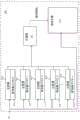
Fig. 4A and 4B illustrate an example implementation of a repetitive SCA countermeasure suitable for multiple-input repetitive attacks. Although specific reference is made to a smart card, the example implementation of the duplicate SCA countermeasure shown in fig. 4A and 4B is applicable to any computing device that receives input and is subject to multiple-input duplicate attacks. Referring to fig. 4A, a smart card 400 may include a plurality of comparators and memory cells, such as n comparators (402, 404, 406, 408, 410) coupled to n respective memory cells (412, 414, 416, 418, 420). Each comparator may receive a block of information periods and output an activity detection signal to counter 422. The counter 422 is coupled to receive the output from each comparator and output an out-of-limit signal to the crypto-engine 424.
As described with respect to fig. 3, the memory cells (e.g., 412, 414, 416, 418, 420) may be registers, such as D-type registers, or suitable non-volatile memory (NVM). Each memory cell has a size to store a cycle of information received via the I/O pin. Further, in some cases, the comparator is a 64-bit comparator. In some cases, the comparator includes a plurality of smaller comparators, each of which is capable of processing a number of bits of the data block within the information period. The multiple storage units (e.g., 412, 414, 416, 418, 420) may be part of the memory storage within the cryptographic engine 424, part of other memory storage on the smart card 400, or a separate storage on the smart card 400. Each comparator (e.g., 402, 404, 406, 408, 410) compares a previously stored information period in a storage location (e.g., 412, 414, 416, 418, 420) associated with the comparator to a newly received information period. If any comparator outputs a signal indicating that the newly received information period matches the previously stored information period, the counter 422 will be incremented.
Each of the n comparators (402, 404, 406, 408, 410) may receive a complete cycle of information from an I/O pin. In some cases, the comparators are connected in series and fill in incoming information cycles similar to a first-in-first-out operation before performing the comparison operation. In some cases, the comparators are connected in parallel so that incoming information cycles are directed to the appropriate comparator before the comparison is performed. Either configuration may be operated such that not all comparators are populated and used for comparison during operation.
In some cases, more than one counter may be used; and allows for the configuration to provide a limit value for the counter.
Referring to fig. 4B, the countermeasures included in the smart card 450 may be similar to those described with respect to the smart card 400 of fig. 4A, but include circuitry 440 that directs the storage of appropriate input data in a memory unit. A circuit 440 is coupled to each comparator (402, 404, 406, 408, 410) to receive the comparator's output: the output of the comparator is a comparison between the received input data of the information cycle and the input data stored in the respective storage unit (412, 414, 416, 418, 420); and if the output of the comparator indicates a mismatch, storing the received input data in the selected one of the memory cells.
Within the counter 422 may be a set of counters, one for each comparator. A single match between a newly received information period and a previously stored information period does not necessarily indicate an attack. The smart card designer can determine how many repeating information cycles are acceptable before implementing the countermeasures. For example, an attack may be considered possible if there are more than 3 repeated information cycles since the last reset. If the counter 422 (either across all counters or by a single counter within the counter 422) exceeds a predetermined acceptable level, the counter (or other circuitry coupled to the counter) may output an out-of-limit signal to the crypto-engine 424 to indicate an attack, such as described with respect to 3; and take appropriate countermeasures. In some cases, no countermeasures are taken in response to the limit signal being exceeded. For example, countermeasures may be taken when a certain number of out-of-limit signals are received.
In some cases, the circuit 440 may determine whether any of the storage cells (412, 414, 416, 418, 420) do not store the previous input data; if all of the memory cells store the previous input data, circuitry 440 may select a random memory cell of the plurality of memory cells and load the received input data for the information cycle into the random memory cell; and if none of the memory cells stores previous input data, one of the empty memory cells may be selected and the received input data for the information cycle is loaded into the empty memory cell. The selection of empty memory cells may be random, according to a predetermined pattern, or sequential. In some cases, circuit 440 may select memory cells according to a predetermined pattern rather than randomly when all memory cells store previously input data. In some cases, each of the n storage units (412, 414, 416, 418, 420) is coupled to a respective full/empty indicator device (426, 428, 430, 432, 434). A full/empty indicator device may be coupled to the circuit 440 to indicate whether the memory cell is an empty information cycle or a full information cycle.
Fig. 5 illustrates a method that may be performed by a repetitive SCA countermeasure using one or more comparators. Method 500 may be performed by any computing device that includes a duplicate SCA countermeasure. In some cases, the method 500 shown in fig. 5 may be performed by a smart card (e.g., as described with respect to the smart cards 300, 400, and 450 of fig. 3, 4A, and 4B). The described duplicate SCA strategy may begin when data is first entered into a smart card (or other computing device) using, for example, I/O connection pins (502). The smart card may be in a wait state until a new input is received (504). Once the new input is received, the new input is loaded into both a compute engine (e.g., a cryptographic engine) and a storage unit (506). Next, the input data is compared to all valid (i.e., non-empty) memory cells (508). This step may occur in a parallel process in which the input data may be compared to all valid memory locations simultaneously — whether there is a single memory location (e.g., as described with respect to smart card 300) or multiple memory locations (e.g., as described with respect to smart cards 400 and 450).
When the input data matches any data already stored in any valid memory cell (510), the counter will be incremented (512). The counter may be checked to see if the number of matches exceeds the limit (514). If the number of matches exceeds the limit, a signal is generated to initiate a countermeasure (516). As some examples, the signal may be an abort signal, an interrupt signal, or a signal to stop the cryptographic operation. If the number of matches does not exceed the limit (as determined during operation 514), the process may return to operation 504 to wait for a new input.
If, during operation 510, the input data does not match any data already stored in any valid memory locations, the smart card/computing device may check whether there are any empty memory locations (518). When there are empty memory locations, the input data may be loaded into the next empty memory location (520), and the process may then return to operation 504 to wait for new input. If there are no empty memory locations, then the memory locations may be selected randomly or in some predetermined pattern (522), and the input data may be loaded into the selected memory locations (524). The process may then return to operation 504 to wait for a new input.
In some cases, one or more comparators and/or method 500 may themselves be implemented in software stored on a computing device and executed by a processor of the computing device. For example, a computer-implemented method may include: receiving input data of an information cycle; comparing the input data with one or more previous input data; incrementing a counter when the input data matches any of the one or more previous input data; and generating a signal to initiate a repeat SCA countermeasure when the counter reaches or exceeds the limit. In some cases, the method further comprises: checking whether there is an empty memory cell when the input data of the information period does not match any previous input data; and loading the input data into a next empty memory cell when there is an empty memory cell, and selecting a memory cell and loading the input data into the selected memory cell when there is no empty memory cell. The selecting of the memory cell may include randomly selecting one of a plurality of memory cells. For example, a random number generator may be used to select a selected memory cell to generate a selection pattern. In some cases, the selected memory cell may be selected according to a predetermined pattern.
Fig. 6 shows a schematic diagram of a smart card implementing the duplicate SCA countermeasure. Referring to fig. 6, the smart card chip 600 may include a cryptographic engine 610; and a pad for: VCC (power supply input), RST (which may be used alone or in combination with internal reset control circuitry), CLK (clock or timing signal), GND (ground-ground or VSS signal), VPP (programming voltage input), I/O (input or output of serial data to a microcontroller internal to the smart card); and optionally two additional connection pads for dedicated inputs (or outputs) or future standards, as described with respect to fig. 1A and 1B. The smart card chip 600 may include a plurality of SCA countermeasures, including countermeasure 1(CM1)620 and countermeasure 2(CM2) 630. CM 1620 may provide a repetitive SCA countermeasure (e.g., as described with respect to fig. 2) using capacitive delays, including a timer circuit and a capacitive delay circuit. CM2630 may provide for repeated SCA countermeasures using one or more comparators (e.g., as described with respect to fig. 3-5). One or both countermeasures may be enabled for a particular chip.
Although a smart card and a cryptographic engine are specifically described and illustrated herein, some of the SCA countermeasures may be applied to any computing device that receives signals such as clock or timing signals, reset signals, ground signals, and power input signals. Furthermore, some of the SCA countermeasures may be applied to any computing device that receives an input signal input in an information cycle.
Although the subject matter has been described in language specific to structural features and/or acts, it is to be understood that the subject matter defined in the appended claims is not necessarily limited to the specific features or acts described above. Rather, the specific features and acts described above are disclosed as example implementations of the claims, and other equivalent features and acts are intended to be within the scope of the claims.