CN112289778B - Display substrate, display device and inspection method for display substrate - Google Patents
Display substrate, display device and inspection method for display substrate Download PDFInfo
- Publication number
- CN112289778B CN112289778B CN202011175489.8A CN202011175489A CN112289778B CN 112289778 B CN112289778 B CN 112289778B CN 202011175489 A CN202011175489 A CN 202011175489A CN 112289778 B CN112289778 B CN 112289778B
- Authority
- CN
- China
- Prior art keywords
- detection
- crack
- base substrate
- substrate
- electrode
- Prior art date
- Legal status (The legal status is an assumption and is not a legal conclusion. Google has not performed a legal analysis and makes no representation as to the accuracy of the status listed.)
- Active
Links
Images


Classifications
-
- H—ELECTRICITY
- H10—SEMICONDUCTOR DEVICES; ELECTRIC SOLID-STATE DEVICES NOT OTHERWISE PROVIDED FOR
- H10K—ORGANIC ELECTRIC SOLID-STATE DEVICES
- H10K59/00—Integrated devices, or assemblies of multiple devices, comprising at least one organic light-emitting element covered by group H10K50/00
- H10K59/80—Constructional details
- H10K59/88—Dummy elements, i.e. elements having non-functional features
-
- H—ELECTRICITY
- H10—SEMICONDUCTOR DEVICES; ELECTRIC SOLID-STATE DEVICES NOT OTHERWISE PROVIDED FOR
- H10K—ORGANIC ELECTRIC SOLID-STATE DEVICES
- H10K59/00—Integrated devices, or assemblies of multiple devices, comprising at least one organic light-emitting element covered by group H10K50/00
- H10K59/80—Constructional details
- H10K59/87—Passivation; Containers; Encapsulations
- H10K59/873—Encapsulations
-
- H—ELECTRICITY
- H10—SEMICONDUCTOR DEVICES; ELECTRIC SOLID-STATE DEVICES NOT OTHERWISE PROVIDED FOR
- H10K—ORGANIC ELECTRIC SOLID-STATE DEVICES
- H10K50/00—Organic light-emitting devices
- H10K50/80—Constructional details
- H10K50/84—Passivation; Containers; Encapsulations
- H10K50/844—Encapsulations
-
- H—ELECTRICITY
- H10—SEMICONDUCTOR DEVICES; ELECTRIC SOLID-STATE DEVICES NOT OTHERWISE PROVIDED FOR
- H10K—ORGANIC ELECTRIC SOLID-STATE DEVICES
- H10K59/00—Integrated devices, or assemblies of multiple devices, comprising at least one organic light-emitting element covered by group H10K50/00
- H10K59/10—OLED displays
- H10K59/12—Active-matrix OLED [AMOLED] displays
- H10K59/122—Pixel-defining structures or layers, e.g. banks
-
- H—ELECTRICITY
- H10—SEMICONDUCTOR DEVICES; ELECTRIC SOLID-STATE DEVICES NOT OTHERWISE PROVIDED FOR
- H10K—ORGANIC ELECTRIC SOLID-STATE DEVICES
- H10K59/00—Integrated devices, or assemblies of multiple devices, comprising at least one organic light-emitting element covered by group H10K50/00
- H10K59/10—OLED displays
- H10K59/12—Active-matrix OLED [AMOLED] displays
- H10K59/131—Interconnections, e.g. wiring lines or terminals
-
- H—ELECTRICITY
- H10—SEMICONDUCTOR DEVICES; ELECTRIC SOLID-STATE DEVICES NOT OTHERWISE PROVIDED FOR
- H10K—ORGANIC ELECTRIC SOLID-STATE DEVICES
- H10K59/00—Integrated devices, or assemblies of multiple devices, comprising at least one organic light-emitting element covered by group H10K50/00
- H10K59/80—Constructional details
- H10K59/87—Passivation; Containers; Encapsulations
- H10K59/873—Encapsulations
- H10K59/8731—Encapsulations multilayered coatings having a repetitive structure, e.g. having multiple organic-inorganic bilayers
-
- H10P74/273—
-
- H—ELECTRICITY
- H10—SEMICONDUCTOR DEVICES; ELECTRIC SOLID-STATE DEVICES NOT OTHERWISE PROVIDED FOR
- H10K—ORGANIC ELECTRIC SOLID-STATE DEVICES
- H10K71/00—Manufacture or treatment specially adapted for the organic devices covered by this subclass
- H10K71/70—Testing, e.g. accelerated lifetime tests
-
- H10P74/203—
-
- H10P74/23—
-
- H10P74/277—
Landscapes
- Engineering & Computer Science (AREA)
- Microelectronics & Electronic Packaging (AREA)
- Manufacturing & Machinery (AREA)
- Physics & Mathematics (AREA)
- Optics & Photonics (AREA)
- Chemical & Material Sciences (AREA)
- Inorganic Chemistry (AREA)
- Electroluminescent Light Sources (AREA)
- Devices For Indicating Variable Information By Combining Individual Elements (AREA)
Abstract
本公开的实施例提供一种显示基板,一种显示装置,以及一种用于显示基板的检测方法。所述显示基板包括:衬底基板,所述衬底基板包括显示区和位于所述显示区至少一侧的外围区;位于所述外围区中的裂纹阻挡件,所述裂纹阻挡件被配置为阻挡裂纹朝所述显示区延伸;设置于所述衬底基板上且覆盖所述显示区的封装结构;以及设置于所述衬底基板上的裂纹检测结构,其中,所述裂纹检测结构位于所述裂纹阻挡件靠近所述显示区的一侧,所述裂纹检测结构在所述衬底基板上的正投影落入所述封装结构在所述衬底基板上的正投影内,所述裂纹检测结构被配置为检测所述封装结构中是否出现裂纹。
Embodiments of the present disclosure provide a display substrate, a display device, and a detection method for a display substrate. The display substrate includes: a base substrate, the base substrate includes a display area and a peripheral area located on at least one side of the display area; a crack stopper located in the peripheral area, the crack stopper is configured to preventing cracks from extending toward the display area; a packaging structure disposed on the base substrate and covering the display area; and a crack detection structure disposed on the base substrate, wherein the crack detection structure is located at the The side of the crack stopper close to the display area, the orthographic projection of the crack detection structure on the base substrate falls within the orthographic projection of the packaging structure on the base substrate, and the crack detection structure A structure is configured to detect the presence of a crack in the package structure.
Description
技术领域technical field
本公开涉及显示技术领域,尤其涉及一种显示基板,一种显示装置,以及一种用于显示基板的检测方法。The present disclosure relates to the field of display technology, and in particular to a display substrate, a display device, and a detection method for a display substrate.
背景技术Background technique
通常,显示装置(例如,有机发光二极管(OLED)显示装置)的显示基板包括无机层,无机层的边缘容易发生裂纹。如果边缘处的裂纹延伸至显示区,则易产生黑斑等显示不良。Generally, a display substrate of a display device (for example, an organic light emitting diode (OLED) display device) includes an inorganic layer, and cracks are prone to occur at edges of the inorganic layer. If the cracks at the edge extend to the display area, display defects such as dark spots are likely to occur.
在本部分中公开的以上信息仅用于对本公开的发明构思的背景的理解,因此,以上信息可包含不构成现有技术的信息。The above information disclosed in this section is only for understanding of the background of the inventive concept of the present disclosure and therefore it may contain information that does not form the prior art.
发明内容Contents of the invention
为了解决上述问题的至少一个方面,本公开实施例提供一种显示基板,一种显示装置,以及一种用于显示基板的检测方法。In order to solve at least one aspect of the above problems, embodiments of the present disclosure provide a display substrate, a display device, and a detection method for a display substrate.
在一个方面,提供一种显示基板,所述显示基板包括:In one aspect, a display substrate is provided, the display substrate comprising:
衬底基板,所述衬底基板包括显示区和位于所述显示区至少一侧的外围区;a base substrate, the base substrate including a display area and a peripheral area located at least one side of the display area;
位于所述外围区中的裂纹阻挡件,所述裂纹阻挡件被配置为阻挡裂纹朝所述显示区延伸;a crack stop located in the peripheral region, the crack stop configured to block cracks from extending toward the display region;
设置于所述衬底基板上且覆盖所述显示区的封装结构;以及a packaging structure disposed on the base substrate and covering the display area; and
设置于所述衬底基板上的裂纹检测结构,a crack detection structure disposed on the base substrate,
其中,所述裂纹检测结构位于所述裂纹阻挡件靠近所述显示区的一侧,所述裂纹检测结构在所述衬底基板上的正投影落入所述封装结构在所述衬底基板上的正投影内,所述裂纹检测结构被配置为检测所述封装结构中是否出现裂纹。Wherein, the crack detection structure is located on the side of the crack blocking member close to the display area, and the orthographic projection of the crack detection structure on the base substrate falls into the package structure on the base substrate In the orthographic projection of , the crack detection structure is configured to detect whether a crack occurs in the package structure.
根据一些示例性的实施例,所述裂纹检测结构被配置为:响应于所述封装结构中出现裂纹,所述裂纹检测结构对入射到其上的光的反射率下降;和/或,响应于所述封装结构中出现裂纹,所述裂纹检测结构的电阻率增大。According to some exemplary embodiments, the crack detection structure is configured to: in response to the occurrence of a crack in the packaging structure, the reflectivity of the crack detection structure to light incident thereon decreases; and/or, in response to A crack occurs in the package structure, and the resistivity of the crack detection structure increases.
根据一些示例性的实施例,所述裂纹检测结构包括检测电极和检测导线,所述检测电极和检测导线电连接;所述检测电极和所述检测导线分别位于不同的导电层中;所述检测电极在所述衬底基板上的正投影与所述检测导线在所述衬底基板上的正投影至少部分重叠。According to some exemplary embodiments, the crack detection structure includes detection electrodes and detection wires, the detection electrodes and detection wires are electrically connected; the detection electrodes and the detection wires are respectively located in different conductive layers; the detection The orthographic projection of the electrode on the base substrate at least partially overlaps with the orthographic projection of the detection wire on the base substrate.
根据一些示例性的实施例,所述检测电极靠近所述裂纹阻挡件的侧部搭接在所述检测导线远离所述裂纹阻挡件的侧部上,以实现所述检测电极和检测导线电连接。According to some exemplary embodiments, the side of the detection electrode close to the crack stopper overlaps the side of the detection wire away from the crack stopper, so as to realize the electrical connection between the detection electrode and the detection wire .
根据一些示例性的实施例,所述显示基板还包括像素界定层,所述像素界定层位于所述检测导线所在的层与所述检测电极所在的层之间;以及所述检测电极通过形成在所述像素界定层中的过孔与所述检测导线电连接。According to some exemplary embodiments, the display substrate further includes a pixel defining layer, the pixel defining layer is located between the layer where the detection wire is located and the layer where the detection electrode is located; and the detection electrode is formed by The via holes in the pixel defining layer are electrically connected to the detection wires.
根据一些示例性的实施例,所述裂纹检测结构包括多个所述检测电极,所述检测导线包括多个检测导线段,所述多个检测电极在所述衬底基板上的正投影和所述多个检测导线段在所述衬底基板上的正投影交替设置,多个所述检测电极中任意两个相邻的检测电极通过一个检测导线段电连接;每一个检测电极包括第一检测电极段和第二检测电极段,所述每一个检测电极包括的第一检测电极段和第二检测电极段相交于一个连接部;以及每一个检测电极包括的第一检测电极段和第二检测电极段中的每一个在所述衬底基板上的正投影相对于与该检测电极相邻的检测导线段在所述衬底基板上的正投影的延伸方向均倾斜设置。According to some exemplary embodiments, the crack detection structure includes a plurality of detection electrodes, the detection wires include a plurality of detection wire segments, and the orthographic projections of the plurality of detection electrodes on the base substrate and the Orthographic projections of the plurality of detection wire segments on the base substrate are arranged alternately, and any two adjacent detection electrodes among the plurality of detection electrodes are electrically connected through a detection wire segment; each detection electrode includes a first detection An electrode segment and a second detection electrode segment, the first detection electrode segment and the second detection electrode segment included in each detection electrode intersect at a connecting portion; and the first detection electrode segment and the second detection electrode segment included in each detection electrode The orthographic projection of each of the electrode segments on the base substrate is obliquely set relative to the extension direction of the orthographic projection of the detection wire segment adjacent to the detection electrode on the base substrate.
根据一些示例性的实施例,所述每一个检测电极包括的连接部位于与该检测电极相邻的检测导线段靠近所述显示区的一侧。According to some exemplary embodiments, the connecting portion included in each detection electrode is located on a side of the detection wire segment adjacent to the detection electrode that is close to the display area.
根据一些示例性的实施例,所述裂纹检测结构包括多个所述检测电极,所述检测导线包括多个检测导线段,所述多个检测导线段连续延伸;每一个检测电极在所述衬底基板上的正投影与多个检测导线段中的至少一个在所述衬底基板上的正投影部分重叠;以及每一个检测电极在所述衬底基板上的正投影相对于与该检测电极重叠的检测导线段在所述衬底基板上的正投影的延伸方向倾斜设置。According to some exemplary embodiments, the crack detection structure includes a plurality of detection electrodes, the detection wire includes a plurality of detection wire segments, and the plurality of detection wire segments extend continuously; The orthographic projection on the base substrate partially overlaps the orthographic projection of at least one of the detection wire segments on the base substrate; and the orthographic projection of each detection electrode on the base substrate is relative to the detection electrode The extension direction of the orthographic projection of the overlapped detection wire segments on the base substrate is arranged obliquely.
根据一些示例性的实施例,所述显示基板还包括设置于所述衬底基板上的阻挡结构,所述阻挡结构位于所述裂纹阻挡件靠近所述显示区的一侧;所述裂纹检测结构在所述衬底基板上的正投影位于所述裂纹阻挡件在所述衬底基板上的正投影与所述阻挡结构在所述衬底基板上的正投影之间。According to some exemplary embodiments, the display substrate further includes a blocking structure disposed on the base substrate, the blocking structure is located on a side of the crack blocking member close to the display area; the crack detection structure The orthographic projection on the backing substrate is between the orthographic projection of the crack stop on the backing substrate and the orthographic projection of the barrier structure on the backing substrate.
根据一些示例性的实施例,所述显示基板还包括设置于所述衬底基板上的发光器件和用于驱动所述发光器件的驱动电路;所述发光器件包括设置于所述衬底基板上的第一电极,设置于所述第一电极远离所述衬底基板一侧的发光层,和设置于所述发光层远离所述衬底基板一侧的第二电极;所述驱动电路至少包括用于供应第一电源电压的电源信号线,所述电源信号线与所述第一电极电连接;以及所述检测导线与所述电源信号线位于同一层,所述检测电极与所述第一电极位于同一层。According to some exemplary embodiments, the display substrate further includes a light emitting device disposed on the base substrate and a driving circuit for driving the light emitting device; the light emitting device includes a light emitting device disposed on the base substrate a first electrode, a light-emitting layer disposed on a side of the first electrode away from the base substrate, and a second electrode disposed on a side of the light-emitting layer away from the base substrate; the drive circuit at least includes A power signal line for supplying a first power supply voltage, the power signal line is electrically connected to the first electrode; and the detection wire is located on the same layer as the power signal line, and the detection electrode is connected to the first electrode The electrodes are on the same layer.
根据一些示例性的实施例,所述检测导线包括单层结构或叠层结构,所述单层结构的材料包括钼,所述叠层结构包括由Ti/Al/Ti形成的叠层结构;和/或,所述检测电极的材料包括镁、银或铝。According to some exemplary embodiments, the detection wire includes a single-layer structure or a laminated structure, the material of the single-layer structure includes molybdenum, and the laminated structure includes a laminated structure formed of Ti/Al/Ti; and /Or, the material of the detection electrode includes magnesium, silver or aluminum.
根据一些示例性的实施例,所述检测导线的厚度在100~200埃之间;和/或,所述检测电极的厚度在100~500埃之间。According to some exemplary embodiments, the detection wire has a thickness between 100-200 angstroms; and/or, the detection electrode has a thickness between 100-500 angstroms.
根据一些示例性的实施例,所述封装结构包括:设置在第二电极远离所述衬底基板一侧的第一封装层;设置在所述第一封装层远离所述衬底基板一侧的第二封装层;以及设置在所述第二封装层远离所述衬底基板一侧的第三封装层,其中,所述第一封装层和所述第三封装层包括无机材料,所述第二封装层包括有机材料;以及所述第二封装层在所述衬底基板上的正投影与所述裂纹检测结构在所述衬底基板上的正投影间隔设置,所述第一封装层和所述第三封装层中的每一个在所述衬底基板上的正投影覆盖所述裂纹检测结构在所述衬底基板上的正投影。According to some exemplary embodiments, the encapsulation structure includes: a first encapsulation layer disposed on a side of the second electrode away from the base substrate; a first encapsulation layer disposed on a side of the first encapsulation layer away from the base substrate a second encapsulation layer; and a third encapsulation layer disposed on a side of the second encapsulation layer away from the base substrate, wherein the first encapsulation layer and the third encapsulation layer include inorganic materials, and the first encapsulation layer includes an inorganic material. The second encapsulation layer includes an organic material; and the orthographic projection of the second encapsulation layer on the base substrate is spaced apart from the orthographic projection of the crack detection structure on the base substrate, the first encapsulation layer and The orthographic projection of each of the third encapsulation layers on the base substrate covers the orthographic projection of the crack detection structure on the base substrate.
在另一方面,提供一种显示装置,所述显示装置包括上述的显示基板。In another aspect, a display device is provided, which includes the above-mentioned display substrate.
在又一方面,提供一种用于显示基板的检测方法,所述显示基板包括:衬底基板,所述衬底基板包括显示区和位于所述显示区至少一侧的外围区;位于所述外围区中的裂纹阻挡件,所述裂纹阻挡件被配置为阻挡裂纹朝所述显示区延伸;设置于所述衬底基板上且覆盖所述显示区的封装结构;以及设置于所述衬底基板上的裂纹检测结构,其中,所述检测方法包括:In yet another aspect, a detection method for a display substrate is provided, the display substrate comprising: a base substrate, the base substrate including a display area and a peripheral area located at least one side of the display area; A crack stopper in the peripheral area, the crack stopper configured to block cracks from extending toward the display area; a package structure disposed on the base substrate and covering the display area; and disposed on the substrate A crack detection structure on a substrate, wherein the detection method includes:
对显示基板的样品进行基准检测,获取所述样品的裂纹检测结构的基准反射率和基准电阻;Carrying out a benchmark test on a sample of the display substrate, and obtaining a benchmark reflectance and a benchmark resistance of the crack detection structure of the sample;
对显示基板的实际产品进行实际检测,获取所述实际产品的裂纹检测结构的实际反射率和实际电阻;Carrying out actual detection on the actual product of the display substrate, and acquiring the actual reflectivity and actual resistance of the crack detection structure of the actual product;
比较所述实际反射率和所述基准反射率,和/或,比较所述实际电阻和所述基准电阻;以及comparing the actual reflectivity to the reference reflectivity, and/or comparing the actual resistance to the reference resistance; and
当所述基准反射率与所述实际反射率的差值大于预设值,和/或,所述实际电阻与所述基准电阻的差值大于预设值时,确定所述显示基板的实际产品的封装结构中存在裂纹。When the difference between the reference reflectance and the actual reflectance is greater than a preset value, and/or the difference between the actual resistance and the reference resistance is greater than a preset value, determine the actual product of the display substrate There are cracks in the package structure.
附图说明Description of drawings
通过下文中参照附图对本公开所作的描述,本公开的其它目的和优点将显而易见,并可帮助对本公开有全面的理解。Other objects and advantages of the present disclosure will be apparent from the following description of the present disclosure with reference to the accompanying drawings, and can help a comprehensive understanding of the present disclosure.
图1是根据本公开的一些示例性实施例的显示基板的平面示意图;FIG. 1 is a schematic plan view of a display substrate according to some exemplary embodiments of the present disclosure;
图2是根据本公开的一些示例性实施例的显示基板沿图1中的线AA’截取的截面示意图;2 is a schematic cross-sectional view of a display substrate taken along line AA' in FIG. 1 according to some exemplary embodiments of the present disclosure;
图3是根据本公开的另一些示例性实施例的显示基板沿图1中的线AA’截取的截面示意图;3 is a schematic cross-sectional view of a display substrate taken along line AA' in FIG. 1 according to other exemplary embodiments of the present disclosure;
图4是根据本公开的另一些示例性实施例的显示基板的平面示意图;4 is a schematic plan view of a display substrate according to other exemplary embodiments of the present disclosure;
图5为根据本公开的一些示例性实施例的显示基板中沿图1中的线BB’的示意截面图,其示意性示出了位于显示区中的像素的驱动电路结构层和发光器件;5 is a schematic cross-sectional view along line BB' in FIG. 1 in a display substrate according to some exemplary embodiments of the present disclosure, which schematically shows a driving circuit structure layer and a light emitting device of a pixel located in a display area;
图6A示意性示出了形成图1中的显示基板的检测导线后的平面图;FIG. 6A schematically shows a plan view after forming detection wires of the display substrate in FIG. 1;
图6B示意性示出了用于形成图1中的显示基板的检测电极的掩模板的平面图;FIG. 6B schematically shows a plan view of a mask used to form the detection electrodes of the display substrate in FIG. 1;
图7A示意性示出了形成图4中的显示基板的检测导线后的平面图;FIG. 7A schematically shows a plan view after forming detection wires of the display substrate in FIG. 4;
图7B示意性示出了用于形成图4中的显示基板的检测电极的掩模板的平面图;FIG. 7B schematically shows a plan view of a mask used to form the detection electrodes of the display substrate in FIG. 4;
图8是根据本公开的一些示例性实施例的用于显示基板的检测方法的流程图;以及8 is a flowchart of a detection method for displaying a substrate according to some exemplary embodiments of the present disclosure; and
图9A和图9B分别是封装结构中无裂纹和有裂纹的情况下进行自动光学检测(即AOI)的示意图。9A and 9B are schematic diagrams of automatic optical inspection (ie, AOI) in the case of no cracks and cracks in the packaging structure, respectively.
需要注意的是,为了清晰起见,在用于描述本公开的实施例的附图中,层、结构或区域的尺寸可能被放大或缩小,即这些附图并非按照实际的比例绘制。It should be noted that for the sake of clarity, in the drawings used to describe the embodiments of the present disclosure, the size of layers, structures or regions may be exaggerated or reduced, that is, the drawings are not drawn according to actual scale.
具体实施方式Detailed ways
在下面的描述中,出于解释的目的,阐述了许多具体细节以提供对各种示例性实施例的全面的理解。然而,明显的是,在不具有这些具体细节或者具有一个或多个等同布置的情况下,可以实施各种示例性实施例。在其它情况下,以框图形式示出了公知的结构和装置,以避免使各种示例性实施例不必要地模糊。此外,各种示例性实施例可以是不同的,但不必是排他的。例如,在不脱离发明构思的情况下,可以在另一示例性实施例中使用或实施示例性实施例的具体形状、配置和特性。In the following description, for purposes of explanation, numerous specific details are set forth in order to provide a thorough understanding of various exemplary embodiments. It is evident, however, that the various exemplary embodiments may be practiced without these specific details, or with one or more equivalent arrangements. In other instances, well-known structures and devices are shown in block diagram form in order to avoid unnecessarily obscuring the various exemplary embodiments. Furthermore, the various exemplary embodiments may be different, but are not necessarily exclusive. For example, the specific shape, configuration, and characteristics of an exemplary embodiment may be used or implemented in another exemplary embodiment without departing from the inventive concept.
在附图中,为了清楚和/或描述的目的,可以放大元件的尺寸和相对尺寸。如此,各个元件的尺寸和相对尺寸不必限于图中所示的尺寸和相对尺寸。当可以不同地实施示例性实施例时,可以与描述的顺序不同地执行具体的工艺顺序。例如,可以基本上同时执行或者以与描述的顺序相反的顺序执行两个连续描述的工艺。此外,同样的附图标记表示同样的元件。In the drawings, the size and relative sizes of elements may be exaggerated for clarity and/or descriptive purposes. As such, the sizes and relative sizes of the respective elements are not necessarily limited to those shown in the drawings. When exemplary embodiments may be implemented differently, a specific process sequence may be performed differently from the described sequence. For example, two consecutively described processes may be performed substantially simultaneously or in an order reverse to that described. Furthermore, the same reference numerals denote the same elements.
当元件被描述为“在”另一元件“上”、“连接到”另一元件或“结合到”另一元件时,所述元件可以直接在所述另一元件上、直接连接到所述另一元件或直接结合到所述另一元件,或者可以存在中间元件。然而,当元件被描述为“直接在”另一元件“上”、“直接连接到”另一元件或“直接结合到”另一元件时,不存在中间元件。用于描述元件之间的关系的其他术语和/或表述应当以类似的方式解释,例如,“在……之间”对“直接在……之间”、“相邻”对“直接相邻”或“在……上”对“直接在……上”等。此外,术语“连接”可指的是物理连接、电连接、通信连接和/或流体连接。此外,X轴、Y轴和Z轴不限于直角坐标系的三个轴,并且可以以更广泛的含义解释。例如,X轴、Y轴和Z轴可彼此垂直,或者可代表彼此不垂直的不同方向。出于本公开的目的,“X、Y和Z中的至少一个”和“从由X、Y和Z构成的组中选择的至少一个”可以被解释为仅X、仅Y、仅Z、或者诸如XYZ、XYY、YZ和ZZ的X、Y和Z中的两个或更多个的任何组合。如文中所使用的,术语“和/或”包括所列相关项中的一个或多个的任何组合和所有组合。When an element is described as being "on," "connected to," or "coupled to" another element, the element may be directly on, directly connected to, or The other element is either directly coupled to the other element, or intervening elements may be present. However, when an element is referred to as being "directly on," "directly connected to" or "directly coupled to" another element, there are no intervening elements present. Other terms and/or expressions used to describe the relationship between elements should be interpreted in a similar fashion, for example, "between" versus "directly between," "adjacent" versus "directly adjacent "Or "on..." versus "directly on..." and so on. Additionally, the term "connected" may refer to a physical connection, an electrical connection, a communicative connection, and/or a fluid connection. In addition, the X-axis, Y-axis, and Z-axis are not limited to the three axes of the rectangular coordinate system, and may be interpreted in a wider sense. For example, the X-axis, Y-axis, and Z-axis may be perpendicular to each other, or may represent different directions that are not perpendicular to each other. For the purposes of this disclosure, "at least one of X, Y, and Z" and "at least one selected from the group consisting of X, Y, and Z" may be interpreted as meaning only X, only Y, only Z, or Any combination of two or more of X, Y, and Z such as XYZ, XYY, YZ, and ZZ. As used herein, the term "and/or" includes any and all combinations of one or more of the associated listed items.
应该理解的是,尽管在这里可使用术语第一、第二等来描述不同的元件,但是这些元件不应受这些术语的限制。这些术语仅是用来将一个元件与另一个元件区分开来。例如,在不脱离示例实施例的范围的情况下,第一元件可以被命名为第二元件,类似地,第二元件可以被命名为第一元件。It will be understood that, although the terms first, second, etc. may be used herein to describe various elements, these elements should not be limited by these terms. These terms are only used to distinguish one element from another. For example, a first element could be termed a second element, and, similarly, a second element could be termed a first element, without departing from the scope of example embodiments.
为了描述的目的,在文中可以使用诸如“在……之下”、“在……下方”、“在……下面”、“下”、“在……上方”、“上”、“在……之上”、“较高的”或“侧”(例如,如在“侧壁”中)等的空间相对术语,从而描述如图中所示的一个元件与另一(或另一些)元件的关系。除了图中描绘的方位之外,空间相对术语还意图包含设备在使用、操作和/或制造中的不同方位。例如,如果图中的设备被翻转,则被描述为“在”其它元件或特征“下方”或“之下”的元件将随后被定位为“在”所述其它元件或特征“上方”。因此,示例性术语“在……下方”可以包含上方和下方两种方位。此外,设备可以被另外定位(例如,旋转90度或者在其它方位处),如此,相应地解释文中使用的空间相对描述语。For descriptive purposes, terms such as "under", "under", "below", "below", "above", "on", "at" may be used in the text ... above", "higher" or "side" (e.g., as in "side wall"), etc., thereby describing one element as shown in the drawings compared to another (or further) elements Relationship. Spatially relative terms are intended to encompass different orientations of the device in use, operation and/or manufacture in addition to the orientation depicted in the figures. For example, if the device in the figures is turned over, elements described as "below" or "beneath" other elements or features would then be oriented "above" the other elements or features. Thus, the exemplary term "below" can encompass both an orientation of above and below. Furthermore, the device may be otherwise positioned (eg, rotated 90 degrees or at other orientations), and as such, the spatially relative descriptors used herein are interpreted accordingly.
除非另外限定,否则文中使用的所有术语(包括技术术语和科学术语)具有与本公开作为其一部分的领域中的普通技术人员所通常理解的含义相同的含义。Unless defined otherwise, all terms (including technical and scientific terms) used herein have the same meaning as commonly understood by one of ordinary skill in the art to which this disclosure forms a part.
本公开的实施例提供一种显示基板,一种显示装置,以及一种用于显示基板的检测方法。所述显示基板包括:衬底基板,所述衬底基板包括显示区和位于所述显示区至少一侧的外围区;位于所述外围区中的裂纹阻挡件,所述裂纹阻挡件被配置为阻挡裂纹朝所述显示区延伸;设置于所述衬底基板上且覆盖所述显示区的封装结构;以及设置于所述衬底基板上的裂纹检测结构,其中,所述裂纹检测结构位于所述裂纹阻挡件靠近所述显示区的一侧,所述裂纹检测结构在所述衬底基板上的正投影落入所述封装结构在所述衬底基板上的正投影内,所述裂纹检测结构被配置为检测所述封装结构中是否出现裂纹。在本公开实施例提供的显示基板中,能够准确判断封装结构的信赖性。Embodiments of the present disclosure provide a display substrate, a display device, and a detection method for a display substrate. The display substrate includes: a base substrate, the base substrate includes a display area and a peripheral area located at least one side of the display area; a crack stopper located in the peripheral area, the crack stopper is configured to preventing cracks from extending toward the display area; a packaging structure disposed on the base substrate and covering the display area; and a crack detection structure disposed on the base substrate, wherein the crack detection structure is located on the The side of the crack stopper close to the display area, the orthographic projection of the crack detection structure on the base substrate falls within the orthographic projection of the packaging structure on the base substrate, and the crack detection structure A structure is configured to detect the presence of a crack in the package structure. In the display substrate provided by the embodiments of the present disclosure, the reliability of the packaging structure can be accurately judged.
图1是根据本公开的一些示例性实施例的显示基板的平面示意图。图2是根据本公开的一些示例性实施例的显示基板沿图1中的线AA’截取的截面示意图。图3是根据本公开的另一些示例性实施例的显示基板沿图1中的线AA’截取的截面示意图。FIG. 1 is a schematic plan view of a display substrate according to some exemplary embodiments of the present disclosure. FIG. 2 is a schematic cross-sectional view of a display substrate taken along line AA' in FIG. 1 according to some exemplary embodiments of the present disclosure. FIG. 3 is a schematic cross-sectional view of a display substrate taken along line AA' in FIG. 1 according to other exemplary embodiments of the present disclosure.
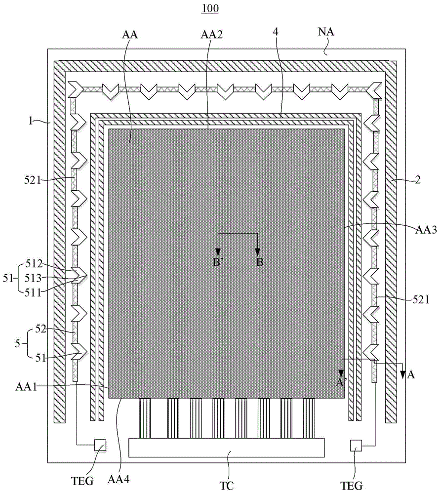
如图1所示,所述显示基板100可以包括衬底基板1,衬底基板1可以被划分为两个区域。例如,衬底基板1包括显示区AA和位于显示区AA至少一侧的外围区NA。例如,外围区NA可以为非显示区,它可位于显示区AA的上侧、下侧、左侧和右侧中的至少一个。图1中示出了外围区NA位于显示区AA的上侧、下侧、左侧和右侧。例如,外围区NA也可仅位于显示区AA的一侧,例如,仅位于显示区AA的上侧、下侧、左侧或右侧。图1中灰色填充处为显示区AA,衬底基板1的其余位置处为外围区NA。例如,显示区AA为显示基板的画面显示区域,为出光区。例如,外围区NA为显示基板的不显示画面的区域,为非出光区。As shown in FIG. 1 , the
如图1所示,所述显示基板100还可以包括设置于衬底基板1上且位于外围区NA中的裂纹阻挡件2,所述裂纹阻挡件被配置为阻挡裂纹朝所述显示区AA延伸。As shown in FIG. 1 , the
参照图2,所述显示基板100还可以包括设置于衬底基板1上且覆盖所述显示区AA的封装结构3。所述封装结构3可以包括由无机层和有机层交替形成的膜层,例如,可以包括依次设置的第一封装层31、第二封装层32以及第三封装层33。例如,第一封装层31和第三封装层33可以由无机材料构成,第二封装层32可以由有机材料构成。Referring to FIG. 2 , the
参照图1至图3,所述显示基板100还可以包括设置于衬底基板1上的裂纹检测结构5。所述裂纹检测结构5位于裂纹阻挡件2靠近所述显示区AA的一侧,所述裂纹检测结构5在所述衬底基板1上的正投影落入封装结构3在所述衬底基板1上的正投影内。Referring to FIGS. 1 to 3 , the
在本公开的实施例中,所述裂纹检测结构5被配置为检测封装结构3中是否出现裂纹。也就是说,借助所述裂纹检测结构5,能够准确判断封装结构3的信赖性。In an embodiment of the present disclosure, the
在一些实施例中,所述裂纹检测结构5被配置为:响应于封装结构3中出现裂纹,所述裂纹检测结构5被腐蚀,例如被水氧腐蚀。例如,在一些实施例中,所述裂纹检测结构5被配置为:响应于封装结构3中出现裂纹,所述裂纹检测结构5对入射到其上的光的反射率下降。可替代地或附加地,在一些实施例中,所述裂纹检测结构5被配置为:响应于封装结构3中出现裂纹,所述裂纹检测结构5的电阻率增大。In some embodiments, the
结合参照图1至图3,所述裂纹检测结构5可以包括检测电极51和检测导线52,检测电极51和检测导线52电连接。检测电极51和检测导线52分别位于不同的导电层中。例如,检测电极51所在的导电层可以位于检测导线52所在的导电层远离衬底基板1的一侧。检测电极51在所述衬底基板1上的正投影与检测导线52在所述衬底基板1上的正投影至少部分重叠。Referring to FIG. 1 to FIG. 3 , the
例如,如图2所示,检测电极51靠近裂纹阻挡件2的侧部搭接在检测导线52远离裂纹阻挡件2的侧部上,以实现所述检测电极51和检测导线52之间的电连接。For example, as shown in FIG. 2 , the side portion of the
例如,如图3所示,所述显示基板100还可以包括像素界定层PDL,像素界定层PDL位于所述检测导线52所在的层与所述检测电极51所在的层之间。检测电极51通过形成在所述像素界定层PDL中的过孔VH1与检测导线52电连接。For example, as shown in FIG. 3 , the
参照图1,在一些实施例中,所述裂纹检测结构5可以包括多个所述检测电极51,所述检测导线52可以包括多个检测导线段521。Referring to FIG. 1 , in some embodiments, the
例如,显示区AA在衬底基板1上的正投影可以呈大致矩形形状。显示区AA可以具有四个侧面,即第一侧面AA1(图1中的左侧面)、第二侧面AA2(图1中的上侧面)、第三侧面AA3(图1中的右侧面)和第四侧面AA4(图1中的下侧面)。For example, the orthographic projection of the display area AA on the
在显示区AA的第一侧面AA1、第二侧面AA2和第三侧面AA3的外侧,均设置有所述检测电极51和检测导线段521。所述多个检测电极51在所述衬底基板1上的正投影和所述多个检测导线段521在所述衬底基板1上的正投影交替设置,多个所述检测电极51中任意两个相邻的检测电极51通过一个检测导线段521电连接。通过这样的方式,多个检测导线段521将多个检测电极51电连接起来。On the outside of the first side AA1 , the second side AA2 and the third side AA3 of the display area AA, the
继续参照图1,每一个检测电极51包括第一检测电极段511和第二检测电极段512,每一个检测电极51包括的第一检测电极段511和第二检测电极段512相交于一个连接部513。在图1所示的平面图中,连接部513以“连接点”的形式被示出。例如,每一个检测电极51包括的连接部513位于与该检测电极51相邻的检测导线段521靠近所述显示区AA的一侧。也就是说,每一个检测电极51在衬底基板1上的正投影呈现为人字形。例如,每一个检测电极51在衬底基板1上的正投影呈现为顶点(即连接点)朝向显示区AA的人字形。结合参照图1,位于第一侧面AA1外侧的每一个检测电极51在衬底基板1上的正投影呈现为顶点朝向右侧的人字形;位于第二侧面AA2外侧的每一个检测电极51在衬底基板1上的正投影呈现为顶点朝向下侧的人字形;位于第三侧面AA3外侧的每一个检测电极51在衬底基板1上的正投影呈现为顶点朝向左侧的人字形。Continuing to refer to FIG. 1, each
每一个检测电极51包括的第一检测电极段511和第二检测电极段512中的每一个在所述衬底基板1上的正投影相对于与该检测电极51相邻的检测导线段521在所述衬底基板1上的正投影的延伸方向均倾斜设置。例如,以位于第一侧面AA1外侧的一个检测电极51为例,其包括第一检测电极段511和第二检测电极段512,与该检测电极51相邻的检测导线段521沿图1中的竖直方向延伸,该检测电极51的第一检测电极段511和第二检测电极段512相对于竖直方向均倾斜设置。这样,可以在有限的空间内尽可能地增加每一个检测电极51的有效长度,以保证每一个检测电极51的电阻的稳定性,此外,还可以提升显示基板的可弯折性能。The orthographic projection of each of the first
图4是根据本公开的另一些示例性实施例的显示基板的平面示意图。如图4所示,所述裂纹检测结构5可以包括多个所述检测电极51,所述检测导线52包括多个检测导线段521,所述多个检测导线段521可以连续延伸。例如,在图4的实施例中,显示基板包括3个检测导线段521,即位于第一侧面AA1外侧的第一检测导线段521,位于第二侧面AA2外侧的第二检测导线段521,位于第三侧面AA3外侧的第三检测导线段521。第一检测导线段可以与第二检测导线段直接相连,第二检测导线段可以与第三检测导线段直接相连,从而形成围绕显示区AA的三个侧面的连续延伸结构。FIG. 4 is a schematic plan view of a display substrate according to other exemplary embodiments of the present disclosure. As shown in FIG. 4 , the
继续参照图4,每一个检测电极51在所述衬底基板1上的正投影与多个检测导线段521中的至少一个在所述衬底基板1上的正投影部分重叠。例如,位于第一侧面AA1外侧的每一个检测电极51与第一检测导线段521的正投影彼此部分重叠,位于第二侧面AA2外侧的每一个检测电极51与第二检测导线段521的正投影彼此部分重叠,位于第三侧面AA3外侧的每一个检测电极51与第三检测导线段521的正投影彼此部分重叠。此外,位于左上侧的拐角处的检测电极51可以与第一检测导线段521的正投影部分重叠,还与第二检测导线段521的正投影部分重叠。位于右上侧的拐角处的检测电极51可以与第二检测导线段521的正投影部分重叠,还与第三检测导线段521的正投影部分重叠。Continuing to refer to FIG. 4 , the orthographic projection of each
在该实施例中,每一个检测电极51在所述衬底基板1上的正投影相对于与该检测电极51重叠的检测导线段521在所述衬底基板1上的正投影的延伸方向倾斜设置。以此方式,可以在有限的空间内尽可能地增加每一个检测电极51的有效长度,以保证每一个检测电极51的电阻的稳定性,此外,还可以提升显示基板的可弯折性能。In this embodiment, the orthographic projection of each
参照图1和图4,所述显示基板还可以包括测试电路TC和测试元件组TEG。测试电路TC和测试元件组TEG可以设置在第四侧面AA4的外侧。例如,测试电路TC可以被配置为给设置于显示区AA中的各个像素提供测试信号。测试元件组TEG可以被配置为给所述裂纹检测结构5提供测试信号。例如,测试电路TC和测试元件组TEG可以通过相同的工艺形成。这样,无需通过额外的构图工艺来形成所述测试元件组TEG,有利于简化制造工艺。Referring to FIGS. 1 and 4 , the display substrate may further include a test circuit TC and a test element group TEG. The test circuit TC and the test element group TEG may be disposed outside the fourth side AA4. For example, the test circuit TC may be configured to provide test signals to respective pixels disposed in the display area AA. The test element group TEG may be configured to provide test signals to the
例如,在利用电学测试设备对测试元件组TEG进行测试时,电学测试设备上的多个测试针脚呈固定方式排列。测试元件组TEG可以包括多个测试接口(即测试垫),该多个测试接口与所述多个测试针脚一一对应排列,以便进行对应检测,即,接收对应的检测信号。For example, when the electrical test equipment is used to test the test element group TEG, a plurality of test pins on the electrical test equipment are arranged in a fixed manner. The test element group TEG may include a plurality of test interfaces (ie, test pads), which are arranged in one-to-one correspondence with the plurality of test pins, so as to perform corresponding detection, that is, to receive corresponding detection signals.
所述显示基板100可以包括两个测试元件组TEG,即靠近第一侧面AA1设置的第一测试元件组TEG和靠近第三侧面AA3设置的第二测试元件组TEG。第一测试元件组TEG与位于第一侧面AA1外侧的一个检测导线段521(左下角位置处)电连接,第二测试元件组TEG与位于第三侧面AA3外侧的一个检测导线段521(右下角位置处)电连接,位于这两个检测导线段521之间的多个检测电极51和多个检测导线段521相互交替且彼此电连接。以此方式,可以将检测信号提供给各个检测电极51。The
参照图2和图3,所述显示基板100还可以包括设置于所述衬底基板1上的阻挡结构4,所述阻挡结构4位于所述裂纹阻挡件2靠近所述显示区AA的一侧。例如,所述阻挡结构4可以用于阻挡有机封装材料。在形成上述封装结构3的有机封装层时,可以采用喷墨打印等工艺,通过设置所述阻挡结构4,可以阻挡有机封装材料朝向阻挡结构4远离显示区AA的一侧。Referring to FIG. 2 and FIG. 3, the
在本公开的实施例中,所述裂纹检测结构5位于阻挡结构4和裂纹阻挡件2之间。即,所述裂纹检测结构5在所述衬底基板1上的正投影位于所述裂纹阻挡件2在所述衬底基板1上的正投影与所述阻挡结构4在所述衬底基板1上的正投影之间。In an embodiment of the present disclosure, the
例如,所述显示基板100可以包括多个裂纹阻挡件2和多个阻挡结构4。所述裂纹检测结构5位于最靠近裂纹阻挡件2的阻挡结构4和最靠近阻挡结构4的裂纹阻挡件2之间。For example, the
参照图2和图3,所述显示基板100可以包括设置在衬底基板1上的绝缘层,例如,该绝缘层可以至少包括层间绝缘层IDL。裂纹阻挡件2可以包括形成在该绝缘层IDL中的至少一个沟槽21,例如多个沟槽21。通过在绝缘层中形成多个沟槽21,可以避免在裂纹阻挡件2外侧的绝缘层中的裂纹朝向显示区AA延伸,有利于提高显示基板的封装信赖性。Referring to FIGS. 2 and 3 , the
可选地,裂纹阻挡件2还可以包括设置在沟槽21远离衬底基板1一侧的有机层膜层(将在下文中进一步说明)。Optionally, the
图5为根据本公开的一些示例性实施例的显示基板中沿图1中的线BB’的示意截面图,其示意性示出了位于显示区AA中的像素的驱动电路结构层和发光器件。参照图5,显示基板100可以包括设置在衬底基板1上的驱动电路结构层和发光器件。5 is a schematic cross-sectional view along line BB' in FIG. 1 in a display substrate according to some exemplary embodiments of the present disclosure, which schematically shows a driving circuit structure layer and a light emitting device of a pixel located in the display area AA. . Referring to FIG. 5 , a
示例性地,图5示出驱动电路结构层的驱动晶体管Qd。驱动晶体管Qd包括有源层121、栅电极123、源电极125以及漏电极127。Exemplarily, FIG. 5 shows the driving transistor Qd of the driving circuit structure layer. The driving transistor Qd includes an
有源层121可设置在衬底基板1上。驱动电路结构层还可包括设置在有源层121和栅电极123之间的第一绝缘层122。第一绝缘层122可将有源层121和栅电极123彼此绝缘。驱动电路结构层还可包括设置在栅电极123和源电极125之间以及在栅电极123和漏电极127之间的第二绝缘层124,以及设置在栅绝缘层124远离衬底基板11一侧的层间绝缘层IDL。源电极125和漏电极127可分别经由形成在绝缘层中的接触孔CH1和CH2电连接到有源层121。The
驱动电路结构层还可包括设置在源电极125和漏电极127上的平坦化层PLN。The driving circuit structure layer may further include a planarization layer PLN disposed on the
虽然未在图5中具体示出,但是开关晶体管可具有与驱动晶体管Qd基本相同的结构或者与驱动晶体管Qd类似的结构,但是示例性实施例不限于此。即,可替代地,开关晶体管和驱动晶体管Qd可具有不同的结构。例如,开关晶体管的有源层和驱动晶体管Qd的有源层121可置于不同的层上。Although not specifically shown in FIG. 5 , the switching transistor may have substantially the same structure as the driving transistor Qd or a similar structure to the driving transistor Qd, but exemplary embodiments are not limited thereto. That is, alternatively, the switching transistor and the driving transistor Qd may have different structures. For example, the active layer of the switching transistor and the
应该理解,驱动电路结构层还可以包括电容Cst,参照图5,电容Cst包括相对且间隔设置的第一极板C1和第二极板C2。例如,第一极板C1可以与栅电极123位于同一层,第二极板C2可以位于栅绝缘层124远离衬底基板11的一侧。例如,第一极板C1和第二极板C2均可以由与栅电极123相同的材料构成。It should be understood that the driving circuit structure layer may also include a capacitor Cst. Referring to FIG. 5 , the capacitor Cst includes a first plate C1 and a second plate C2 that are opposite and spaced apart. For example, the first plate C1 may be located on the same layer as the
结合参照图2、图3和图5,在一些示例性实施例中,驱动电路结构层不仅可设置在显示区AA中,还可设置在外围区NA中。例如,驱动电路结构层还可以包括电连接至驱动集成电路(IC)的多条走线,这些走线的一部分可以位于显示区AA中,另一部分可以位于外围区NA中。例如,所述走线可以包括用于提供初始化电压信号的初始化电压信号线Vint,用于提供VSS电压信号的电源信号线VSS等。初始化电压信号线Vint和电源信号线VSS可以与上述源电极125和漏电极127位于同一导电层中。Referring to FIGS. 2 , 3 and 5 in combination, in some exemplary embodiments, the driving circuit structure layer may be disposed not only in the display area AA but also in the peripheral area NA. For example, the driving circuit structure layer may further include a plurality of wires electrically connected to the driving integrated circuit (IC), some of these wires may be located in the display area AA, and the other part may be located in the peripheral area NA. For example, the wiring may include an initialization voltage signal line Vint for providing an initialization voltage signal, a power signal line VSS for providing a VSS voltage signal, and the like. The initialization voltage signal line Vint and the power signal line VSS may be located in the same conductive layer as the above-mentioned
所述驱动电路结构层还可以包括驱动电路GOA。例如,该驱动电路可以位于显示区AA的至少一侧。在图2所示的实施例中,驱动电路位于初始化电压信号线Vint和电源信号线VSS之间。所述驱动电路可以用于驱动显示基板中的各个像素进行显示。例如,所述驱动电路可以包括栅极驱动电路和数据驱动电路。数据驱动电路用于依据时钟信号定时将输入的数据顺序锁存并将锁存的数据转换成模拟信号后输入到显示基板的各条数据线上。栅极驱动电路通常由移位寄存器实现,移位寄存器将时钟信号转换成开启/关断电压,分别输出到显示基板的各条栅线上。The driving circuit structure layer may also include a driving circuit GOA. For example, the driving circuit can be located on at least one side of the display area AA. In the embodiment shown in FIG. 2 , the driving circuit is located between the initialization voltage signal line Vint and the power signal line VSS. The driving circuit can be used to drive each pixel in the display substrate to display. For example, the driving circuit may include a gate driving circuit and a data driving circuit. The data driving circuit is used for sequentially latching the input data according to the timing of the clock signal and converting the latched data into analog signals and inputting them to each data line of the display substrate. The gate driving circuit is usually implemented by a shift register, which converts the clock signal into an on/off voltage, which is respectively output to each gate line of the display substrate.
例如,所述驱动电路可以采用GOA技术,即Gate Driver on Array。在GOA技术中,将栅极驱动电路直接设置于阵列基板上,以代替外接驱动芯片。每个GOA单元作为一级移位寄存器,每级移位寄存器与一条栅线连接,通过各级移位寄存器依序轮流输出开启电压,实现像素的逐行扫描。在一些实施例中,每级移位寄存器也可以与多条栅线连接。这样,可以适应显示基板高分辨率、窄边框的发展趋势。For example, the driving circuit may adopt GOA technology, that is, Gate Driver on Array. In the GOA technology, the gate driving circuit is directly disposed on the array substrate instead of an external driving chip. Each GOA unit is used as a first-level shift register, and each level of shift register is connected to a gate line, and the turn-on voltage is sequentially output through each level of shift register to realize progressive scanning of pixels. In some embodiments, each stage of the shift register can also be connected to multiple gate lines. In this way, it can adapt to the development trend of display substrates with high resolution and narrow borders.
发光器件可包括第一电极131、发光层132以及第二电极133。第一电极131可以设置在平坦化层PLN远离衬底基板1的一侧。例如,所述第一电极131可以是OLED的正极和负极中的一个,例如负极;所述第二电极133可以是OLED的正极和负极中的另一个,例如正极。例如,所述发光层132可以是有机发光层。The light emitting device may include a
例如,参照图2和图3,所述显示基板100还可以包括导电连接部128,导电连接部128可以设置在电源信号线VSS远离衬底基板1一侧的导电层中。导电连接部128的一部分与电源信号线VSS接触,以与电源信号线VSS电连接。导电连接部128的另一部分可与第一电极131接触,以与第一电极131电连接。以此方式,实现电源信号线VSS与第一电极131的电连接,从而将VSS电压信号提供给第一电极131。For example, referring to FIG. 2 and FIG. 3 , the
所述像素界定层PDL可以位于导电连接部128远离所述衬底基板1的一侧。所述像素界定层PDL可以具有开孔129。开孔129暴露所述导电连接部128的至少一部分。第一电极131的一部分填充于该开孔129中,从而与导电连接部128接触。The pixel defining layer PDL may be located on a side of the
例如,导电连接部128在衬底基板1上的正投影与平坦化层PLN在衬底基板1上的正投影部分重叠。并且,导电连接部128中形成有多个通孔1281,多个通孔1281分别暴露平坦化层PLN的一部分。通过设置这些通孔1281,有利于释放在高温制程中释放的水汽等排放气体。For example, the orthographic projection of the
所述显示基板100还可以包括隔垫物PS。所述阻挡结构4可以包括靠近所述裂纹检测结构5的第一阻挡结构41和远离所述裂纹检测结构5的第二阻挡结构42。即,第一阻挡结构41比第二阻挡结构42更靠近裂纹检测结构5。The
第一阻挡结构41可以包括叠层结构,例如,可以包括第一阻挡层411、第二阻挡层412和第三阻挡层413。第一阻挡层411可与平坦化层PLN位于同一层,第二阻挡层412可与像素界定层PDL位于同一层,第三阻挡层413可与隔垫物PS位于同一层。第一阻挡结构41至少覆盖电源信号线VSS靠近裂纹检测结构5的侧面,以及覆盖导电连接部128靠近裂纹检测结构5的侧面,从而保护电源信号线VSS的该侧面和导电连接部128的该侧面。The
第二阻挡结构42可以包括叠层结构,例如,第二阻挡结构42可以包括第一阻挡子层421和第二阻挡子层422。第一阻挡子层421可与像素界定层PDL位于同一层,第二阻挡子层422可与隔垫物PS位于同一层。第二阻挡结构42在衬底基板1上的正投影可以落入电源信号线VSS和导电连接部128中每一个在衬底基板1上的正投影内。The
如上所述,所述封装结构3包括依次设置的第一封装层31、第二封装层32以及第三封装层33。例如,第一封装层31和第三封装层33可以由无机材料构成,第二封装层32可以由有机材料构成。第二封装层32在衬底基板1上的正投影与阻挡结构4在衬底基板1上的正投影间隔设置。例如,第二封装层32在衬底基板1上的正投影与第二阻挡结构42在衬底基板1上的正投影间隔设置。即,第二封装层32靠近裂纹阻挡件2的侧面位于阻挡结构4的内侧。As mentioned above, the encapsulation structure 3 includes the
第一封装层31和第三封装层33均延伸到阻挡结构4的外侧,它们均覆盖裂纹检测结构5。第一封装层31和第三封装层33中每一个在衬底基板1上的正投影均覆盖裂纹检测结构5在衬底基板1上的正投影。这样,裂纹检测结构5可以用来检测封装结构3中是否存在裂纹。Both the
在本公开的实施例中,裂纹容易通过无机封装层延伸进显示区,通过将裂纹检测结构5设置在无机封装层31和33中,有利于检测裂纹是否延伸进封装结构3中。In the embodiments of the present disclosure, cracks easily extend into the display area through the inorganic encapsulation layer, and by disposing the
在本公开的实施例中,所述检测导线52与所述电源信号线VSS位于同一层,所述检测电极51与所述第一电极131位于同一层。In the embodiment of the present disclosure, the
例如,所述检测导线52包括单层结构或叠层结构,所述单层结构的材料包括钼,所述叠层结构包括由Ti/Al/Ti形成的叠层结构。所述检测电极51的材料包括镁、银或铝。For example, the
例如,所述检测导线52的厚度在100~200埃之间。所述检测电极51的厚度在100~500埃之间。For example, the
在本公开的实施例中,所述检测导线52与所述电源信号线VSS位于同一层,这样,检测导线52可与电源信号线VSS等位于同一导电层中的部件通过同一构图工艺形成。图6A示意性示出了形成图1中的显示基板的检测导线52后的平面图。结合参照图1至图6A,检测导线52可与电源信号线VSS等位于同一导电层中的部件通过同一构图工艺形成。In the embodiment of the present disclosure, the
所述检测电极51与所述第一电极131位于同一层,这样,所述检测电极51与所述第一电极131可以通过同一构图工艺形成。图6B示意性示出了用于形成图1中的显示基板的检测电极51的掩模板的平面图。结合参照图1至图6B,该掩模板可以包括一个第一开口OH1和多个第二开口OH2。第一开口OH1为一个较大尺寸的开口,用于形成第一电极131。多个第二开口OH2用于形成多个检测电极51。例如,可以在蒸镀工艺中,通过该掩模板,同时形成第一电极131和检测电极51。这样,有利于简化制造工艺。The
相应地,图7A示意性示出了形成图4中的显示基板的检测导线52后的平面图。图7B示意性示出了用于形成图4中的显示基板的检测电极51的掩模板的平面图。该掩模板可以包括一个第一开口OH1和多个第二开口OH2。第一开口OH1为一个较大尺寸的开口,用于形成第一电极131。多个第二开口OH2用于形成多个检测电极51。结合参照图1至图7B,检测导线52可与电源信号线VSS等位于同一导电层中的部件通过同一构图工艺形成。所述检测电极51与所述第一电极131可以通过同一构图工艺形成。这样,有利于简化制造工艺。Correspondingly, FIG. 7A schematically shows a plan view after forming the
图8是根据本公开的一些示例性实施例的用于显示基板的检测方法的流程图。所述检测方法可以包括以下步骤。FIG. 8 is a flowchart of a detection method for a display substrate according to some exemplary embodiments of the present disclosure. The detection method may include the following steps.
在步骤S81中,对显示基板100的样品进行基准检测,获取所述样品的裂纹检测结构的基准反射率和基准电阻。In step S81 , a reference test is performed on a sample of the
需要说明的是,显示基板100的样品指的是确定封装结构3中没有裂纹的显示基板。在对该样品进行检测后,可以获取封装结构3中没有裂纹的情况下裂纹检测结构的各个基准值,例如,基准反射率和基准电阻。It should be noted that the sample of the
在步骤S82中,对显示基板的实际产品进行实际检测,获取所述实际产品的裂纹检测结构的实际反射率和实际电阻。In step S82 , the actual product of the display substrate is actually detected, and the actual reflectivity and actual resistance of the crack detection structure of the actual product are obtained.
需要说明的是,显示基板100的实际产品指的是生产线上制造出的实际产品。这些实际产品在制造出来后,在实际加工制程的影响下,例如,切割时可能在显示基板的边缘处产生裂纹,该裂纹可能延伸进封装结构3中。It should be noted that the actual product of the
在步骤S83中,比较所述实际反射率和所述基准反射率,和/或,比较所述实际电阻和所述基准电阻。In step S83, the actual reflectance is compared with the reference reflectance, and/or the actual resistance is compared with the reference resistance.
在步骤S84中,当所述基准反射率与所述实际反射率的差值大于预设值,和/或,所述实际电阻与所述基准电阻的差值大于预设值时,确定所述显示基板的实际产品的封装结构中存在裂纹。In step S84, when the difference between the reference reflectance and the actual reflectance is greater than a preset value, and/or the difference between the actual resistance and the reference resistance is greater than a preset value, it is determined that the There is a crack in the package structure of the actual product showing the substrate.
可选地,在上述步骤S81中,还可以获取所述样品的裂纹检测结构的基准图像。例如,可以对样品的裂纹检测结构进行拍照,以获取该基准图像。Optionally, in the above step S81, a reference image of the crack detection structure of the sample may also be acquired. For example, the crack detection structure of the sample can be photographed to obtain this reference image.
在步骤S82中,还获取实际产品的裂纹检测结构的实际图像。例如,可以对实际产品的裂纹检测结构进行拍照,以获取该实际图像。In step S82, an actual image of the crack detection structure of the actual product is also acquired. For example, a crack detection structure of an actual product may be photographed to obtain the actual image.
在步骤S83中,还比较基准图像和实际图像的差异。并且,在步骤S84中,当所述基准图像和所述实际图像的差异较大时,判断所述裂纹检测结构是否被腐蚀,并且,响应于所述裂纹检测结构被腐蚀,确定所述显示基板的实际产品的封装结构存在裂纹。In step S83, the difference between the reference image and the actual image is also compared. And, in step S84, when the difference between the reference image and the actual image is large, it is judged whether the crack detection structure is corroded, and in response to the crack detection structure being corroded, it is determined that the display substrate There are cracks in the packaging structure of the actual product.
例如,在一些示例性实施例中,比较基准图像和实际图像,可以发现:裂纹检测结构的实际图像中存在较多被腐蚀的痕迹。即,该显示基板的裂纹检测结构已经被腐蚀。在情况下,可以确定该显示基板的封装结构3中存在裂纹。For example, in some exemplary embodiments, comparing the reference image and the actual image, it can be found that there are many traces of corrosion in the actual image of the crack detection structure. That is, the crack detection structure of the display substrate has been corroded. In this case, it can be determined that there is a crack in the packaging structure 3 of the display substrate.
图9A和图9B分别是封装结构中无裂纹和有裂纹的情况下进行自动光学检测(即AOI)的示意图。如图9A所示,封装结构3中无裂纹,裂纹检测结构5没有被水氧等腐蚀。在进行AOI检测过程中,入射光基本都被裂纹检测结构5反射回来,即反射率较高。如图9B所示,封装结构3中有裂纹,裂纹检测结构5被水氧等腐蚀。在进行AOI检测过程中,入射光照射到裂纹检测结构5上会产生类似于漫反射的效果,AOI检测设备接收到的反射光减少,即反射率较低。也就是说,裂纹检测结构5在封装结构中无裂纹的情况下的反射率大于在封装结构中有裂纹的情况下的反射率。通过判断所述基准反射率与所述实际反射率的差值是否大于预设值,即能够确定封装结构3中是否有裂纹。9A and 9B are schematic diagrams of automatic optical inspection (ie, AOI) in the case of no cracks and cracks in the packaging structure, respectively. As shown in FIG. 9A , there is no crack in the package structure 3 , and the
需要说明的是,此处的“预设值”可以是绝对值,例如,在10%以上;也可以是相对值,例如,此处的“预设值”可以用所述差值与所述基准反射率的比值来表示,例如,如果所述差值与所述基准反射率的比值大于5%,则认为所述基准反射率与所述实际反射率的差值大于预设值。It should be noted that the "preset value" here can be an absolute value, for example, above 10%; it can also be a relative value, for example, the "preset value" here can be the difference between the difference and the For example, if the ratio of the difference to the reference reflectance is greater than 5%, it is considered that the difference between the reference reflectance and the actual reflectance is greater than a preset value.
类似,结合参照图1和图4,可以借助测试元件组TEG,对裂纹检测结构5的电学性能进行检测,例如检测它的电阻率。在封装结构3中无裂纹的情况下,裂纹检测结构5没有被腐蚀,其导电性能良好,电阻率较小。在封装结构3中有裂纹的情况下,裂纹检测结构5被水氧等腐蚀,其导电性能变差,电阻率较大。也就是说,裂纹检测结构5在封装结构中有裂纹的情况下的电阻率大于在封装结构中无裂纹的情况下的电阻率。通过判断所述实际电阻率与所述基准电阻率的差值是否大于预设值,即能够确定封装结构3中是否有裂纹。Similarly, referring to FIG. 1 and FIG. 4 in conjunction, the electrical performance of the
需要说明的是,此处的“预设值”可以是绝对值,例如,在0.1*10-8(Ω·m)以上;也可以是相对值,例如,此处的“预设值”可以用所述差值与所述基准电阻率的比值来表示,例如,如果所述差值与所述基准电阻率的比值大于5%,则认为所述实际电阻率与所述基准电阻率的差值大于预设值。It should be noted that the "preset value" here can be an absolute value, for example, above 0.1*10 -8 (Ω·m); it can also be a relative value, for example, the "preset value" here can be Expressed by the ratio of the difference to the reference resistivity, for example, if the ratio of the difference to the reference resistivity is greater than 5%, the difference between the actual resistivity and the reference resistivity is considered The value is greater than the preset value.
在本公开的另一些实施例中,还提供一种显示装置。所述显示装置可以包括上述显示基板。例如,所述显示装置可以是智能电话、移动电话、视频电话、电子书阅读器、台式电脑(PC)、膝上型PC、上网本PC、个人数字助理(PDA)、便携式多媒体播放器(PMP)、数字音频播放器、移动医疗设备、相机、可穿戴设备(例如头戴式设备、电子服饰、电子手环或智能手表)等。In other embodiments of the present disclosure, a display device is also provided. The display device may include the above-mentioned display substrate. For example, the display device may be a smartphone, mobile phone, video phone, e-book reader, desktop computer (PC), laptop PC, netbook PC, personal digital assistant (PDA), portable multimedia player (PMP) , digital audio players, mobile medical devices, cameras, wearable devices (such as head-mounted devices, electronic clothing, electronic bracelets or smart watches), etc.
虽然根据本公开的总体发明构思的一些实施例已被图示和说明,本领域普通技术人员将理解,在不远离本公开的总体发明构思的原则和精神的情况下,可对这些实施例做出改变,本公开的范围以权利要求和它们的等同物限定。Although some embodiments according to the general inventive concept of the present disclosure have been illustrated and described, those of ordinary skill in the art will understand that, without departing from the principles and spirit of the general inventive concept of the present disclosure, modifications can be made to these embodiments. Without modification, the scope of the present disclosure is defined by the claims and their equivalents.
Claims (10)
Priority Applications (3)
| Application Number | Priority Date | Filing Date | Title |
|---|---|---|---|
| CN202011175489.8A CN112289778B (en) | 2020-10-28 | 2020-10-28 | Display substrate, display device and inspection method for display substrate |
| US17/788,922 US12532650B2 (en) | 2020-10-28 | 2021-09-01 | Display substrate, display device, and detection method for crack in encapsulation structure |
| PCT/CN2021/116001 WO2022088955A1 (en) | 2020-10-28 | 2021-09-01 | Display substrate, display device, and detection method for display substrate |
Applications Claiming Priority (1)
| Application Number | Priority Date | Filing Date | Title |
|---|---|---|---|
| CN202011175489.8A CN112289778B (en) | 2020-10-28 | 2020-10-28 | Display substrate, display device and inspection method for display substrate |
Publications (2)
| Publication Number | Publication Date |
|---|---|
| CN112289778A CN112289778A (en) | 2021-01-29 |
| CN112289778B true CN112289778B (en) | 2023-02-07 |
Family
ID=74373854
Family Applications (1)
| Application Number | Title | Priority Date | Filing Date |
|---|---|---|---|
| CN202011175489.8A Active CN112289778B (en) | 2020-10-28 | 2020-10-28 | Display substrate, display device and inspection method for display substrate |
Country Status (3)
| Country | Link |
|---|---|
| US (1) | US12532650B2 (en) |
| CN (1) | CN112289778B (en) |
| WO (1) | WO2022088955A1 (en) |
Families Citing this family (6)
| Publication number | Priority date | Publication date | Assignee | Title |
|---|---|---|---|---|
| CN112289778B (en) * | 2020-10-28 | 2023-02-07 | 京东方科技集团股份有限公司 | Display substrate, display device and inspection method for display substrate |
| CN113360024B (en) * | 2021-06-18 | 2024-04-12 | 京东方科技集团股份有限公司 | Touch panel and crack detection method thereof |
| US12326412B2 (en) | 2022-01-07 | 2025-06-10 | Chengdu Boe Optoelectronics Technology Co., Ltd. | Display substrates, display apparatuses and methods of detecting cracks in display substrates |
| KR20230137612A (en) * | 2022-03-22 | 2023-10-05 | 엘지디스플레이 주식회사 | Display apparatus |
| CN116864507B (en) * | 2022-03-25 | 2026-01-30 | 京东方科技集团股份有限公司 | Display substrate |
| CN114944111B (en) * | 2022-05-23 | 2023-12-05 | 京东方科技集团股份有限公司 | Display panel and display device |
Family Cites Families (19)
| Publication number | Priority date | Publication date | Assignee | Title |
|---|---|---|---|---|
| US6091131A (en) * | 1998-04-28 | 2000-07-18 | International Business Machines Corporation | Integrated circuit having crack stop for interlevel dielectric layers |
| US20130082843A1 (en) * | 2011-09-30 | 2013-04-04 | Apple Inc. | Detection of fracture of display panel or other patterned device |
| US9983452B2 (en) * | 2014-07-15 | 2018-05-29 | Huawei Technologies Co., Ltd. | Method for detecting substrate crack, substrate, and detection circuit |
| KR102356028B1 (en) * | 2015-02-06 | 2022-01-26 | 삼성디스플레이 주식회사 | Display device |
| US9614183B2 (en) * | 2015-04-01 | 2017-04-04 | Apple Inc. | Organic light-emitting diode displays with crack detection and crack propagation prevention circuitry |
| KR102417143B1 (en) | 2015-04-29 | 2022-07-05 | 삼성디스플레이 주식회사 | Display device |
| JP6444914B2 (en) * | 2016-03-02 | 2018-12-26 | 東芝メモリ株式会社 | Semiconductor device |
| KR102518427B1 (en) * | 2016-03-14 | 2023-04-05 | 삼성디스플레이 주식회사 | Display device |
| US11087670B2 (en) * | 2016-08-19 | 2021-08-10 | Apple Inc. | Electronic device display with monitoring circuitry utilizing a crack detection resistor |
| KR102718898B1 (en) * | 2016-12-06 | 2024-10-17 | 삼성디스플레이 주식회사 | Display device |
| KR102439673B1 (en) * | 2017-06-19 | 2022-09-05 | 삼성디스플레이 주식회사 | Display apparatus |
| KR102056678B1 (en) * | 2017-11-23 | 2019-12-17 | 엘지디스플레이 주식회사 | Organic light emitting display device |
| WO2019157271A2 (en) * | 2018-02-09 | 2019-08-15 | Massachusetts Institute Of Technology | Systems and methods for crack detection |
| CN108598282B (en) * | 2018-05-11 | 2021-02-26 | 京东方科技集团股份有限公司 | Display substrate and detection method and detection device thereof |
| KR102737652B1 (en) * | 2018-10-26 | 2024-12-04 | 삼성디스플레이 주식회사 | Display apparatus and method of manufacturing the same |
| KR102642351B1 (en) * | 2018-12-31 | 2024-02-28 | 엘지디스플레이 주식회사 | Electroluminescence display apparatus |
| CN109872634A (en) * | 2019-03-28 | 2019-06-11 | 武汉华星光电半导体显示技术有限公司 | A kind of display panel |
| CN111509026B (en) | 2020-05-27 | 2023-02-07 | 京东方科技集团股份有限公司 | Display panel, method for detecting cracks thereof, and display device |
| CN112289778B (en) * | 2020-10-28 | 2023-02-07 | 京东方科技集团股份有限公司 | Display substrate, display device and inspection method for display substrate |
-
2020
- 2020-10-28 CN CN202011175489.8A patent/CN112289778B/en active Active
-
2021
- 2021-09-01 WO PCT/CN2021/116001 patent/WO2022088955A1/en not_active Ceased
- 2021-09-01 US US17/788,922 patent/US12532650B2/en active Active
Also Published As
| Publication number | Publication date |
|---|---|
| US20230046867A1 (en) | 2023-02-16 |
| WO2022088955A1 (en) | 2022-05-05 |
| CN112289778A (en) | 2021-01-29 |
| US12532650B2 (en) | 2026-01-20 |
Similar Documents
| Publication | Publication Date | Title |
|---|---|---|
| CN112289778B (en) | Display substrate, display device and inspection method for display substrate | |
| US12396327B2 (en) | Array substrate structure | |
| CN108258016B (en) | Flexible display device | |
| CN106229332B (en) | Display panel, manufacturing method thereof and flexible display device | |
| KR102879461B1 (en) | Display device and method for fabricating the same | |
| CN106896609A (en) | A kind of array base palte and the display device including it | |
| KR102860751B1 (en) | Display device and method for fabricating the same | |
| CN113380656A (en) | Display substrate to be cut, display substrate and display device thereof | |
| CN110190087A (en) | display screen | |
| CN109216305B (en) | Display device | |
| EP4586790A2 (en) | Display device and method of providing the same | |
| JP2025516505A (en) | display device | |
| US9626014B2 (en) | Touch display panel and manufacturing method thereof | |
| US10847751B2 (en) | Display device including a thin film encapsulating layer and method of manufacturing the same | |
| CN110738936A (en) | Component substrate and splicing electronic device | |
| CN120164392A (en) | Display device and test circuit board | |
| KR102768108B1 (en) | Display apparatus and method of manufacturing the same | |
| TW202537489A (en) | Display device | |
| US20230397461A1 (en) | Display device and manufacturing method of the same | |
| US12336413B2 (en) | Display panel, display device, and manufacturing method of display panel | |
| KR102890482B1 (en) | Display device and method of manufacturing the same | |
| CN116360617A (en) | display device | |
| CN116264808A (en) | touch display device | |
| KR20210103614A (en) | Display device | |
| CN113903783A (en) | Display panel and method for manufacturing the same |
Legal Events
| Date | Code | Title | Description |
|---|---|---|---|
| PB01 | Publication | ||
| PB01 | Publication | ||
| SE01 | Entry into force of request for substantive examination | ||
| SE01 | Entry into force of request for substantive examination | ||
| GR01 | Patent grant | ||
| GR01 | Patent grant |