CN112216767A - Fabrication of semiconductor photosensitive devices - Google Patents
Fabrication of semiconductor photosensitive devices Download PDFInfo
- Publication number
- CN112216767A CN112216767A CN202010646126.1A CN202010646126A CN112216767A CN 112216767 A CN112216767 A CN 112216767A CN 202010646126 A CN202010646126 A CN 202010646126A CN 112216767 A CN112216767 A CN 112216767A
- Authority
- CN
- China
- Prior art keywords
- layer
- germanium
- support
- doped
- substrate
- Prior art date
- Legal status (The legal status is an assumption and is not a legal conclusion. Google has not performed a legal analysis and makes no representation as to the accuracy of the status listed.)
- Granted
Links
- 239000004065 semiconductor Substances 0.000 title claims abstract description 20
- 238000004519 manufacturing process Methods 0.000 title claims abstract description 16
- GNPVGFCGXDBREM-UHFFFAOYSA-N germanium atom Chemical compound [Ge] GNPVGFCGXDBREM-UHFFFAOYSA-N 0.000 claims abstract description 123
- 229910052732 germanium Inorganic materials 0.000 claims abstract description 116
- 238000000034 method Methods 0.000 claims description 32
- 239000000758 substrate Substances 0.000 claims description 28
- 230000007547 defect Effects 0.000 claims description 16
- VYPSYNLAJGMNEJ-UHFFFAOYSA-N Silicium dioxide Chemical compound O=[Si]=O VYPSYNLAJGMNEJ-UHFFFAOYSA-N 0.000 claims description 12
- 239000012212 insulator Substances 0.000 claims description 12
- 238000000407 epitaxy Methods 0.000 claims description 10
- 238000005498 polishing Methods 0.000 claims description 6
- 235000012239 silicon dioxide Nutrition 0.000 claims description 6
- 239000000377 silicon dioxide Substances 0.000 claims description 6
- XUIMIQQOPSSXEZ-UHFFFAOYSA-N Silicon Chemical compound [Si] XUIMIQQOPSSXEZ-UHFFFAOYSA-N 0.000 claims description 5
- 229910052710 silicon Inorganic materials 0.000 claims description 5
- 239000010703 silicon Substances 0.000 claims description 5
- FGUUSXIOTUKUDN-IBGZPJMESA-N C1(=CC=CC=C1)N1C2=C(NC([C@H](C1)NC=1OC(=NN=1)C1=CC=CC=C1)=O)C=CC=C2 Chemical compound C1(=CC=CC=C1)N1C2=C(NC([C@H](C1)NC=1OC(=NN=1)C1=CC=CC=C1)=O)C=CC=C2 FGUUSXIOTUKUDN-IBGZPJMESA-N 0.000 claims description 4
- 229910052739 hydrogen Inorganic materials 0.000 claims description 3
- 239000001257 hydrogen Substances 0.000 claims description 3
- -1 hydrogen ions Chemical class 0.000 claims description 3
- 238000002513 implantation Methods 0.000 claims description 3
- 238000000992 sputter etching Methods 0.000 claims description 3
- 235000012431 wafers Nutrition 0.000 claims 1
- 230000036961 partial effect Effects 0.000 description 10
- 230000008901 benefit Effects 0.000 description 8
- 239000013078 crystal Substances 0.000 description 8
- 230000005855 radiation Effects 0.000 description 7
- 229910052751 metal Inorganic materials 0.000 description 6
- 239000002184 metal Substances 0.000 description 6
- 238000005468 ion implantation Methods 0.000 description 5
- 230000002829 reductive effect Effects 0.000 description 5
- 238000001514 detection method Methods 0.000 description 4
- 230000035945 sensitivity Effects 0.000 description 4
- 230000000694 effects Effects 0.000 description 3
- 238000005530 etching Methods 0.000 description 3
- 230000006872 improvement Effects 0.000 description 3
- 239000000463 material Substances 0.000 description 3
- 230000004048 modification Effects 0.000 description 3
- 238000012986 modification Methods 0.000 description 3
- 230000002441 reversible effect Effects 0.000 description 3
- 238000010292 electrical insulation Methods 0.000 description 2
- 150000004678 hydrides Chemical class 0.000 description 2
- 150000002500 ions Chemical class 0.000 description 2
- 230000004075 alteration Effects 0.000 description 1
- 229910052782 aluminium Inorganic materials 0.000 description 1
- XAGFODPZIPBFFR-UHFFFAOYSA-N aluminium Chemical compound [Al] XAGFODPZIPBFFR-UHFFFAOYSA-N 0.000 description 1
- 230000015572 biosynthetic process Effects 0.000 description 1
- 230000015556 catabolic process Effects 0.000 description 1
- 239000004020 conductor Substances 0.000 description 1
- 238000006731 degradation reaction Methods 0.000 description 1
- 239000002019 doping agent Substances 0.000 description 1
- 230000014509 gene expression Effects 0.000 description 1
- 238000010438 heat treatment Methods 0.000 description 1
- GPRLSGONYQIRFK-UHFFFAOYSA-N hydron Chemical compound [H+] GPRLSGONYQIRFK-UHFFFAOYSA-N 0.000 description 1
- 239000007943 implant Substances 0.000 description 1
- 230000000670 limiting effect Effects 0.000 description 1
- 230000003071 parasitic effect Effects 0.000 description 1
- 238000003825 pressing Methods 0.000 description 1
- 230000009467 reduction Effects 0.000 description 1
- 230000000717 retained effect Effects 0.000 description 1
- 238000007669 thermal treatment Methods 0.000 description 1
Images


Classifications
-
- H—ELECTRICITY
- H10—SEMICONDUCTOR DEVICES; ELECTRIC SOLID-STATE DEVICES NOT OTHERWISE PROVIDED FOR
- H10F—INORGANIC SEMICONDUCTOR DEVICES SENSITIVE TO INFRARED RADIATION, LIGHT, ELECTROMAGNETIC RADIATION OF SHORTER WAVELENGTH OR CORPUSCULAR RADIATION
- H10F71/00—Manufacture or treatment of devices covered by this subclass
- H10F71/139—Manufacture or treatment of devices covered by this subclass using temporary substrates
-
- H—ELECTRICITY
- H10—SEMICONDUCTOR DEVICES; ELECTRIC SOLID-STATE DEVICES NOT OTHERWISE PROVIDED FOR
- H10F—INORGANIC SEMICONDUCTOR DEVICES SENSITIVE TO INFRARED RADIATION, LIGHT, ELECTROMAGNETIC RADIATION OF SHORTER WAVELENGTH OR CORPUSCULAR RADIATION
- H10F71/00—Manufacture or treatment of devices covered by this subclass
- H10F71/121—The active layers comprising only Group IV materials
- H10F71/1212—The active layers comprising only Group IV materials consisting of germanium
-
- H—ELECTRICITY
- H10—SEMICONDUCTOR DEVICES; ELECTRIC SOLID-STATE DEVICES NOT OTHERWISE PROVIDED FOR
- H10F—INORGANIC SEMICONDUCTOR DEVICES SENSITIVE TO INFRARED RADIATION, LIGHT, ELECTROMAGNETIC RADIATION OF SHORTER WAVELENGTH OR CORPUSCULAR RADIATION
- H10F30/00—Individual radiation-sensitive semiconductor devices in which radiation controls the flow of current through the devices, e.g. photodetectors
- H10F30/20—Individual radiation-sensitive semiconductor devices in which radiation controls the flow of current through the devices, e.g. photodetectors the devices having potential barriers, e.g. phototransistors
- H10F30/21—Individual radiation-sensitive semiconductor devices in which radiation controls the flow of current through the devices, e.g. photodetectors the devices having potential barriers, e.g. phototransistors the devices being sensitive to infrared, visible or ultraviolet radiation
- H10F30/22—Individual radiation-sensitive semiconductor devices in which radiation controls the flow of current through the devices, e.g. photodetectors the devices having potential barriers, e.g. phototransistors the devices being sensitive to infrared, visible or ultraviolet radiation the devices having only one potential barrier, e.g. photodiodes
- H10F30/223—Individual radiation-sensitive semiconductor devices in which radiation controls the flow of current through the devices, e.g. photodetectors the devices having potential barriers, e.g. phototransistors the devices being sensitive to infrared, visible or ultraviolet radiation the devices having only one potential barrier, e.g. photodiodes the potential barrier being a PIN barrier
-
- H—ELECTRICITY
- H10—SEMICONDUCTOR DEVICES; ELECTRIC SOLID-STATE DEVICES NOT OTHERWISE PROVIDED FOR
- H10F—INORGANIC SEMICONDUCTOR DEVICES SENSITIVE TO INFRARED RADIATION, LIGHT, ELECTROMAGNETIC RADIATION OF SHORTER WAVELENGTH OR CORPUSCULAR RADIATION
- H10F77/00—Constructional details of devices covered by this subclass
- H10F77/10—Semiconductor bodies
- H10F77/12—Active materials
- H10F77/122—Active materials comprising only Group IV materials
Landscapes
- Light Receiving Elements (AREA)
- Recrystallisation Techniques (AREA)
- Thin Film Transistor (AREA)
Abstract
本公开涉及一种制造半导体器件的方法,包括以下相继步骤:a)在覆盖第一支撑件的锗层上形成掺杂锗;b)以第二支撑件覆盖所述掺杂锗;以及c)去除所述第一支撑件。

The present disclosure relates to a method of fabricating a semiconductor device comprising the following sequential steps: a) forming doped germanium on a germanium layer covering a first support; b) covering the doped germanium with a second support; and c) The first support is removed.
Description
The present application claims the benefit of priority from french patent application No. FR19/07664, the contents of which are hereby incorporated by reference in their entirety to the maximum extent allowed by law.
Technical Field
The present disclosure relates generally to semiconductor devices and, in particular, to photosensitive devices comprised of germanium.
Background
Photosensitive devices composed of germanium are used in infrared radiation (e.g., having a wavelength in the range of from about 0.9 μm to about 1.6 μm) detection applications. Such a device comprises, for example, a photodiode, i.e. a diode that conducts current when it receives infrared radiation.
The light-sensitive devices are mostly arranged in an array, for example in an image sensor. Each photosensitive device receives radiation originating from a portion of the scene. The array then enables an infrared image to be obtained in the scene. Each pixel of the image corresponds to a photosensitive device in the array.
Disclosure of Invention
There is a need for improvements in known semiconductor-based devices and methods of manufacturing the same.
There is a need to reduce parasitic currents, known as dark currents, that flow through the photosensitive device without receiving radiation.
There is a need to reduce the difference in operating characteristics (such as dark current and/or detection sensitivity) between photosensitive devices that are intended to be identical (e.g., arranged in an array).
There is a need to improve the manufacturing efficiency and reliability of photosensitive devices.
Embodiments overcome all or part of the disadvantages of known semiconductor-based devices.
Embodiments overcome all or part of the disadvantages of known methods of fabricating semiconductor-based devices.
Embodiments provide a method of fabricating a photosensitive device with reduced dark current.
Embodiments provide a method of fabricating a photosensitive device having reduced differences between its operating characteristics.
Embodiments provide a more reliable manufacturing method than known methods and provide a more reliable photosensitive device than known devices.
An embodiment provides a method of manufacturing a semiconductor device, comprising the following successive steps: a) forming a buried hydride layer in the germanium substrate under a portion of the substrate forming the germanium layer by implantation of hydrogen ions; b) covering the substrate with a first support; c) removing the buried layer and a portion of the substrate on a side of the buried layer opposite to the first support while leaving the germanium layer covering the first support in place; d) forming doped germanium on the germanium layer; e) covering the doped germanium with a second support; and f) removing the first support, the method further comprising, prior to step d), epitaxially growing intrinsic germanium on the germanium layer.
According to an embodiment, the first support and/or the second support is a silicon wafer.
According to an embodiment, the germanium of the substrate is intrinsic and monocrystalline.
According to an embodiment, an intrinsic germanium epitaxy step is performed after step c).
According to an embodiment, at step c) an insulator is located between the substrate and the first support, said insulator being removed after step e).
According to an embodiment, at step d), the doped germanium is formed by epitaxy.
According to an embodiment, the germanium layer is intrinsic.
According to an embodiment, the germanium layer is monocrystalline and preferably has less than 10 defects per square centimeter.
According to an embodiment, the germanium layer has a thickness greater than or equal to about 1 μm.
According to an embodiment, at step e), an insulating layer is located between the doped germanium and the second support, the insulating layer preferably comprising silicon dioxide.
According to an embodiment, at step e), the method comprises the steps of: covering the doped germanium with a first portion of the insulating layer; covering a second support with a second portion of the insulating layer; and performing molecular bonding between the first portion and the second portion of the insulating layer.
According to an embodiment, the method comprises after step f), epitaxially growing doped germanium on the germanium layer having a conductivity type different from the conductivity type of the doped germanium formed at step d).
According to an embodiment, at step f), the first support is removed by ion etching and/or polishing.
According to an embodiment, the device is a photodiode.
Brief description of the drawings
The foregoing features and advantages, and other features and advantages, are described in detail in the following description of specific embodiments, given by way of illustration and not of limitation with reference to the accompanying drawings.
FIG. 1 is a partially simplified cross-sectional view of an example of a device to which the described embodiments are applied;
FIG. 2 is a partial simplified cross-sectional view illustrating steps of an embodiment of a method of fabricating a semiconductor-based device;
FIG. 3 is a partial simplified cross-sectional view illustrating another step of the method;
FIG. 4 is a partial simplified cross-sectional view illustrating another step of the method;
FIG. 5 is a partial simplified cross-sectional view illustrating another step of the method;
FIG. 6 is a partial simplified cross-sectional view illustrating another step of the method;
FIG. 7 is a partial simplified cross-sectional view illustrating another step of the method;
FIG. 8 is a partial simplified cross-sectional view illustrating another step of the method;
FIG. 9 is a partial simplified cross-sectional view illustrating another step of the method;
FIG. 10 is a partial simplified cross-sectional view illustrating another step of the method;
FIG. 11 is a simplified cross-sectional view showing another step of the method; and
fig. 12 is a simplified cross-sectional view showing a variation of the step of fig. 11.
Detailed Description
Like features have been identified with like reference numerals in the various figures. In particular, structural and/or functional features that are common among the various embodiments may have the same references and may be configured with the same structural, dimensional, and material properties.
For clarity, only steps and elements useful for understanding the embodiments described in this disclosure are shown and described in detail. In particular, various steps of forming and/or removing (such as epitaxy, etching, polishing, thermal treatment, etc.) various insulator, semiconductor, or metal regions or layers have not been described in detail, and the described embodiments are consistent with common steps of forming and/or removing insulator, semiconductor, or metal regions or layers.
Unless otherwise indicated, when two elements are referred to as being connected together, this means a direct connection without any intervening elements other than conductors, and when two elements are referred to as being coupled together, this means that the two elements may be connected via one or more other elements or may be coupled via one or more other elements.
In the following disclosure, unless otherwise indicated, when referring to a qualifier for an absolute position, such terms as "front", "back", "upper", "lower", "left", "right", etc., or to a qualifier for a relative position, such as "above …", "below …", "higher", "lower", etc., or to a qualifier for an orientation, such as "horizontal", "vertical", etc., refer to the orientation shown in the figures.
Unless specifically stated otherwise, expressions of "about", "approximately", "substantially" and "approximately …" mean within 10%, and preferably within 5%.
Fig. 1 is a partially simplified cross-sectional view of an example of a device to which the embodiment is applied. More particularly, the device in this example is a germanium-based photodiode 100.
As an example, the photodiode 100 is located on a support 102. The support 102 is generally plate-like. The support 102 is preferably a semiconductor wafer portion, and the support 102 is more preferably covered with an insulator (not shown) on its upper surface.
The photodiode 100 is of the PIN type, i.e. it comprises an intrinsic semiconductor region between doped semiconductor regions of opposite type. When the semiconductor is not intentionally doped or when its doping level is less than 10 per cubic centimeter16One atom, preferably less than 10 per cubic centimeter15When atomic, a semiconductor is referred to herein as "intrinsic". The photodiode 100 comprises a stack in the following order starting from the support 102: a P-type doped germanium layer 110, an intrinsic germanium layer 120, and an N-type doped germanium layer 130.
The layers 110 and 130 are connected to the anode contact region a of the photodiode and the cathode region K of the photodiode, respectively. As a variant, the layers 110 and 130 exchange their conductivity types N and P and exchange the contact areas a and K.
In operation, the photodiode is reverse biased. Infrared radiation received by the photodiode causes a current 122 that flows through the intrinsic layer 120 to the P-doped layer 110 in the N-doped layer 130 of the photodiode. In other words, the PIN photodiode 100 is of a vertical type, i.e., the current 122 flows from one of the main surfaces (upper and lower surfaces) of the intrinsic layer 120 to the other. One of the advantages of a vertical photodiode is that it takes up less space for the same sensitivity than a photodiode where the intrinsic and doped regions are not stacked. This enables, for example, the number of pixels of the obtained infrared image to be increased for the same sensitivity and the same size of the image sensor.
In some applications, the photodiode is reverse biased during radiation detection. More particularly, when infrared radiation is received by the photodiode, the reverse voltage is sufficient to obtain the avalanche effect. Advantageously, the avalanche effect results in increased sensitivity relative to a photodiode that does not use the avalanche effect.
The embodiments described in the following figures provide an improvement in the crystal quality of the intrinsic layer 120 relative to known vertical PIN photodiodes. In other words, in such embodiments, intrinsic layer 120 is preferably monocrystalline and has a particularly low number of defects (such as dislocations) or no defects (such as dislocations) across at least a portion of its thickness. This enables a dark current in the photodiode to be reduced.
Furthermore, when photodiodes designed to be identical are manufactured, there is a substantial difference between the operating characteristics of the photodiodes obtained. The fact that the number of defects of the lattice of the intrinsic layer 120 is reduced, for example, to a value of less than 10 defects per square centimeter, enables the difference in operating characteristics due to the difference between the positions and the number of defects to be reduced.
Furthermore, the reduction in the number of defects of the lattice of the intrinsic layer 120 makes it possible to reduce the risk that the photodiode does not have desired operating characteristics and is rejected, for example, during testing after manufacturing. Thus improving the manufacturing efficiency of the photodiode. But also reduces the risk of photodiode degradation and thus improves the reliability of the photodiode.
Fig. 2-11 are partial simplified cross-sectional views illustrating successive steps of an embodiment of a method of fabricating a semiconductor-based device. More particularly, the device is, as an example, a photodiode of the type described with respect to fig. 1.
At the step of fig. 2-4, a germanium layer 210B is formed overlying support 250. More particularly, in the example of these steps, layer 210B is part of substrate 210 and is formed and mounted on support 250 by a method of the type known by the trade name "Smart Cut".
At the step of fig. 2, a germanium substrate 210 is provided. The substrate 210 preferably has a plate shape, for example, the substrate 210 is a germanium wafer.
More preferably, the crystal lattice of the substrate 210 exhibits no or almost no defects, i.e. the number of defects is less than 10 per square centimeter, preferably less than 5 per square centimeter. To achieve this, the substrate may be obtained by the czochralski method.
Hydrogen ions are implanted from the upper surface of the substrate 210 (in fig. 2) to form a buried hydride layer 220 in the substrate 210. The buried layer 220 is located below the germanium layer 210B. The remaining portion of the substrate 210 corresponds to the portion 210A located below the buried layer 220. As a result of this step, layer 210B is preferably intrinsic and monocrystalline, and is defect-free or nearly defect-free. Layer 210B is intended to form all or part of the intrinsic layer 120 (fig. 1) of future photodiodes.
The depth of the buried layer 220 is related to the energy of the implanted ions. The depth is greater than the thickness of germanium layer 210B. For example, the thickness of germanium layer 210B is greater than 0.1 μm, more preferably greater than 0.2 μm, and even more preferably greater than 0.5 μm. Preferably, the implant is provided such that the thickness of the germanium layer 210B is as large as possible, i.e., typically greater than or equal to about 1 μm. Thus, germanium layer 210B may advantageously form all or most of the intrinsic layer 120 of future photodiodes. This will enable the above advantages to be maximized in future photodiodes due to the crystal quality of the intrinsic layer 120.
Preferably, an electrically insulating or dielectric layer 230 is formed on germanium layer 210B. The insulating layer 230 is more preferably formed after the hydrogen ion implantation. The insulating layer 230 may be comprised of silicon dioxide.
In parallel, support 250 is provided before or after the formation of the structure comprising portion 210A and layers 220, 210B and 230. The support member 250 is generally plate-shaped, having two opposing major surfaces (a lower surface and an upper surface in fig. 2). The support 250 is temporary, i.e. it is intended to be removed in a subsequent step (step of fig. 9). Preferably, the support 250 is a semiconductor wafer, for example made of silicon. As a variant, any other support suitable for a method of the type known under the trade name "Smart Cut" and capable of being removed in a subsequent step can be used.
Preferably, an electrical insulation layer 260 is formed on the lower surface of the supporter 250. More preferably, the material of the insulating layer 260 is the same as that of the insulating layer 230.
At the step of fig. 3, germanium layer 210B is covered by support 250. Preferably, for this purpose, insulating layers 230 and 260 are assembled by placing insulating layers 230 and 260 in contact with their accessible (i.e., uncovered) surfaces. Preferably, the assembly is of the molecular bonding type, which is obtained after polishing the surfaces to be in contact with each other, placing the layers in contact with each other and applying pressure. Layers 230 and 260 then form insulator 310 between germanium layer 210B and support 250. The embodiments are not limited to assembly by molecular bonding and are compatible with any current steps that enable the germanium layer to be covered with supports (e.g., by assembling and/or forming supports on the germanium layer).
At the step of fig. 4, the buried layer 220 and the portion 210A of the substrate 210 are removed to leave the germanium layer 210B in place. The structure of fig. 4 is shown inverted relative to the structure of fig. 3, with the elements of fig. 4 covering the upper surface of the support 250 being located on the lower surface of the support 250 in fig. 3. To remove the buried layer 220 and the portion 210A, a heat treatment is performed to cause fracture of the buried layer 220, followed by polishing of the upper surface of the structure shown in fig. 4.
In said embodiment, the steps of fig. 2 to 4 may be replaced by any step that enables to obtain a germanium layer on the support, preferably intrinsic and monocrystalline, and even more preferably with a lattice free or almost free of defects. The support may be any support that can be removed in a subsequent step. For example, the steps of fig. 2-4 may be replaced by providing only a substrate, such as substrate 210, a germanium layer corresponding to a surface portion of the substrate, and the remaining portion of the substrate corresponding to the support. The resulting structure corresponds to that of fig. 4, where the support is comprised of germanium and insulator 310 is omitted. However, the presence of the insulator 310 eases the subsequent removal of the support compared to such an example. The germanium layer may also be obtained, for example, by epitaxy on a doped germanium layer intended to form the doped layer 110 or 130 (fig. 1). However, the fact that germanium layer 210B is provided as part of the substrate facilitates obtaining a defect-free or nearly defect-free single-crystal germanium layer 210B, as compared to germanium epitaxy.
At the step of fig. 5, an intrinsic germanium layer 410 is epitaxially grown on the surface (upper surface) of the germanium layer 210B that was made accessible at the step of fig. 4. Layers 210B and 410 form the intrinsic layer 120 of the future photodiode. For this purpose, the thickness of the epitaxial layer 410 is selected such that the sum of the thicknesses of the layers 210B and 410 corresponds to the desired thickness of the intrinsic layer 120, e.g., the desired thickness is greater than or equal to about 1.5 μm. The thickness of epitaxial layer 410 is, for example, in the range from 20% to 50% of the thickness of germanium layer 210B. As a variation, the steps of fig. 5 are omitted, and the intrinsic layer 120 of the future photodiode is formed from germanium layer 210B. However, in contrast to such a variant, the provision of the layer 410 makes it possible to easily obtain a layer 120 of the desired thickness.
Although the step of fig. 5 is preferably performed after the step of fig. 4 (removing portion 210A of substrate 210), as a variant, it may be provided to form layer 410 on germanium layer 210B before forming insulating layer 230 at the step of fig. 2, germanium layer 210B being intended to be left in place on support 250 at the step of fig. 4. After the step of fig. 4, layer 410 is then located under germanium layer 210B. However, in contrast to such a variant, the fact that the step of fig. 5 is carried out after the step of fig. 4, enables to avoid the risk of thermal budgeting by epitaxy, due to the presence of the spacing between the hydrogenated buried layer 220, the portion 210A and the germanium layer 210B.
At the step of fig. 6, doped germanium is formed on the structure obtained at the step of fig. 5, as described with respect to fig. 1, the doped germanium forming a layer 110 of the future photodiode. In other words, the doped germanium covers the germanium layers 410 and 210B and preferably contacts the layer 410. If the step of fig. 5 is omitted, the doped germanium covers germanium layer 210B and preferably is in contact with germanium layer 210B.
Preferably, the doped germanium layer 100 is formed by epitaxy. This enables a more accurate control of the thickness of the layer 110 and its doping profile, in particular at the junction between the intrinsic layer 120 and the doped germanium of the layer 110, than would otherwise be possible to form the layer 110. This makes it possible to improve the operating characteristics of the photodiodes and to limit the difference in operating characteristics between intended identical photodiodes.
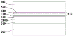
At the step of fig. 7, an electrically insulating or dielectric layer 510 is formed on the doped germanium layer 110. The insulating layer 510 may be composed of silicon dioxide.
There is further provided a support, such as the support 102 described with respect to fig. 1, preferably formed from a silicon wafer.
Preferably, an electrically insulating layer 560 is formed on the lower surface of the support 102, for example, composed of silicon dioxide. More preferably, the material of the insulating layer 510 is the same as that of the insulating layer 560.
At the step of fig. 8, the doped germanium layer 110 is covered by the support 102. Preferably, for this purpose, layers 510 and 560 are assembled by placing layers 510 and 560 in contact with their accessible surfaces. Preferably, the assembly is of the molecular bonding type. The layers 510 and 560 then form an insulating layer 610 between the doped germanium layer 410 and the support 102, the layers 510 and 560 forming a first portion and a second portion, respectively, of the layer 610. As a variant, the layer 610 may be omitted. However, the fact of providing the layer 610 advantageously enables to obtain an electrical insulation between the support 102 and the doped germanium layer 110 in future photodiodes. Furthermore, the fact that the layers 510 and 560 are provided enables molecular bonding to be facilitated with respect to omitting the assembly of these layers. The embodiments are not limited to assembly by molecular bonding and are compatible with the current steps of enabling to cover a doped germanium layer with supports (e.g., by assembling and/or forming supports on the doped germanium layer).
At the step of fig. 9, the support 250 is removed. Insulator 310 is also preferably removed to make germanium layer 210B accessible. The structure of fig. 9 is shown inverted relative to the structure of fig. 8, with the element covering the upper surface of the support 102 in fig. 9 being located on the lower surface of the support 102 in fig. 8. Preferably, the support 250 and the insulator 310 are removed by ion etching and/or polishing.
Thus, in the structure obtained at the step of fig. 9, doped germanium layer 110 is located between support 102 and germanium layer 120. In other words, the doped germanium layer 110 is buried under the upper germanium layer 120.
The present invention may be designed to obtain a doped germanium layer buried under the upper germanium layer by ion implanting dopants through the upper germanium layer. For example, the present invention may be designed to obtain a buried doped germanium layer from germanium layer 210B (such as germanium layer 210B of fig. 4) by doping a lower portion of layer 210B through an upper portion of that layer. The resulting upper germanium layer, however, will have a thickness that is less than the thickness of layer 210.
The steps of fig. 5 to 9 enable the thickness of the upper germanium layer to be increased from a structure such as that of fig. 4, as compared to forming a buried layer by ion implantation. Furthermore, the steps of fig. 5 to 9 enable easier control of the doping profile of the buried layer. Furthermore, the steps of fig. 5 to 9 make it possible to avoid ion implantation through the upper germanium layer, which makes it possible to avoid any risk of modifying this layer during implantation. In particular, in the preferred case in which layer 210B is made of intrinsic single-crystal germanium with no or little defects at the end of the steps of fig. 2 to 4, layer 210B remains made of single-crystal germanium with no or little defects at the end of the steps of fig. 9.
Thus, the steps of fig. 2 to 9 enable in particular to obtain a germanium layer 210B made of a single-crystal germanium having no or almost no defects. More particularly, intrinsic germanium layer 120 of the photodiode is a single crystal with no or little defects across at least a portion of its thickness corresponding to layer 210B. As described above, this provides advantages of reducing dark current, reducing the difference between photodiodes intended to be identical, and increasing reliability and manufacturing efficiency. These advantages are all the more pronounced the thicker the germanium layer 210B is.
Although the steps of fig. 2 to 9 have been described in the specific case of the fabrication of a photodiode, they may be implemented to fabricate any semiconductor-based device of this type comprising a doped germanium layer, such as layer 110, on a support, topped with a germanium region, preferably intrinsic and/or monocrystalline, preferably with no or few defects. In particular, the above-mentioned advantages of steps 5 to 9 are retained for any device of this type.
At the step of fig. 10, an N-type doped layer 130 is formed. The doped germanium layers 110 and 130 of the P and N conductivity types may be interchanged. Thus, layers 110 and 130 have opposite conductivity types. The N-type doped layer is preferably epitaxial, which enables easy control of its thickness and its doping profile.
At the step of fig. 11, a P-doped region 710 is formed by ion implantation extending from the upper surface of the N-doped layer 130 through the N-type layer 130 and the intrinsic layer 120 to the P-doped layer 110. An N-type doped region 730 is formed by ion implantation, separated from the P-region 710 and extending from the upper surface of the N-type layer 130 through at least a portion of the N-type layer 130, preferably up to a level located in the intrinsic layer 120. An insulating layer 740, for example made of silicon dioxide, is then formed on the N-type layer 130 and preferably in contact with the N-type layer 130. The insulating layer 740 has through openings over the P-type region 710 and the N-type region 730. These openings are filled with metal regions 750 and 760 that contact the P-type doped region 710 and the N-type doped region 730, respectively. The doping levels of the P-type doped region 710 and the N-type doped region 730 are preferably higher than the doping levels of the P-type layer 110 and the N-type layer 130, respectively, so that these regions form, with the corresponding metal regions 750 and 760, the anode and cathode contact regions a and K, respectively, of the photodiode.
As an example, a plurality of photodiodes have been formed simultaneously on the support 102. The support 102 and layers 610, 110, 120 and 130 are then cut into individual photodiodes by dicing lines 77.
Fig. 12 is a simplified cross-sectional view showing a modification of the step in fig. 11. This variant is compatible with diodes such as those described In an article by M.Jutzi et al, entitled "Ge-on-Si Pin-phosphors for Vertical and In-Plane detection of 1300to 1580nm Light", published In "ESCIRC 2004-Proceedings of the 34th European Solid-State Device Research Conference" page 345-347.
The structure obtained at the step of fig. 10 is covered with a layer 830 in contact with the upper N-type layer 130. Layer 830 is made of, for example, N-type doped silicon.
All portions of the layers 830, 130, 120, 110 that are outside the location 820 are removed. Such removal is performed, for example, by etching from the upper surface of layer 830 down to at least the upper surface of insulating layer 610.
All remaining portions of layers 830, 130 and 120 that are outside of location 810, which is strictly included in location 830, are removed. More particularly, location 820 extends on either side of location 810. Such removal is performed, for example, by etching from the upper surface of layer 830 down to at least the upper surface of P-type doped germanium layer 110. Thus, portions of layer 110 on either side of location 820 become accessible.
A metal region 750 of anode a, made of aluminum for example, is then formed over and in contact with the accessible portion of layer 110. Metal region 760 of cathode K is formed over and in contact with the remaining portion of layer 830.
The disclosure has described various embodiments and modifications. Those skilled in the art will appreciate that certain features of these embodiments can be combined, and that other variations will readily occur to those skilled in the art.
Finally, the actual implementation of the embodiments and variations in the present disclosure is within the abilities of one of ordinary skill in the art based on the functional descriptions provided above.
Such alterations, modifications, and improvements are intended to be part of this disclosure, and are intended to be within the spirit and scope of the invention. Accordingly, the foregoing description is by way of example only and is not intended as limiting. The invention is limited only as defined in the following claims and the equivalents thereto.
Claims (14)
Applications Claiming Priority (2)
| Application Number | Priority Date | Filing Date | Title |
|---|---|---|---|
| FR1907664 | 2019-07-09 | ||
| FR1907664A FR3098643B1 (en) | 2019-07-09 | 2019-07-09 | Manufacture of a photosensitive semiconductor device |
Publications (2)
| Publication Number | Publication Date |
|---|---|
| CN112216767A true CN112216767A (en) | 2021-01-12 |
| CN112216767B CN112216767B (en) | 2024-04-05 |
Family
ID=68733208
Family Applications (1)
| Application Number | Title | Priority Date | Filing Date |
|---|---|---|---|
| CN202010646126.1A Active CN112216767B (en) | 2019-07-09 | 2020-07-07 | Fabrication of semiconductor photosensitive device |
Country Status (4)
| Country | Link |
|---|---|
| US (1) | US11005002B2 (en) |
| EP (1) | EP3764403B1 (en) |
| CN (1) | CN112216767B (en) |
| FR (1) | FR3098643B1 (en) |
Cited By (1)
| Publication number | Priority date | Publication date | Assignee | Title |
|---|---|---|---|---|
| CN114709233A (en) * | 2022-05-10 | 2022-07-05 | 浙江兴芯半导体有限公司 | Method for integrating germanium p-i-n photodiode into image sensor structure |
Citations (6)
| Publication number | Priority date | Publication date | Assignee | Title |
|---|---|---|---|---|
| CN1159071A (en) * | 1995-10-06 | 1997-09-10 | 佳能株式会社 | Semiconductor substrate and producing method thereof |
| EP1443550A1 (en) * | 2003-01-29 | 2004-08-04 | S.O.I. Tec Silicon on Insulator Technologies S.A. | A method for fabricating a strained crystalline layer on an insulator, a semiconductor structure therefor, and a fabricated semiconductor structure |
| US20060054891A1 (en) * | 2004-09-13 | 2006-03-16 | International Business Machines Corporation | Method of creating defect free high Ge content (>25%) SiGe-on-insulator (SGOI) substrates using wafer bonding techniques |
| CN101192512A (en) * | 2006-11-30 | 2008-06-04 | S.O.I.Tec绝缘体上硅技术公司 | Fabrication method of semiconductor heterostructure |
| US20090061557A1 (en) * | 2006-03-13 | 2009-03-05 | Shin-Etsu Chemical Co., Ltd | Method for manufacturing substrate for photoelectric conversion element |
| US20100275990A1 (en) * | 2009-05-02 | 2010-11-04 | Semiconductor Energy Laboratory Co., Ltd. | Photoelectric conversion device and manufacturing method thereof |
Family Cites Families (10)
| Publication number | Priority date | Publication date | Assignee | Title |
|---|---|---|---|---|
| US6833195B1 (en) * | 2003-08-13 | 2004-12-21 | Intel Corporation | Low temperature germanium transfer |
| US20060021565A1 (en) * | 2004-07-30 | 2006-02-02 | Aonex Technologies, Inc. | GaInP / GaAs / Si triple junction solar cell enabled by wafer bonding and layer transfer |
| US8481845B2 (en) * | 2008-02-05 | 2013-07-09 | Gtat Corporation | Method to form a photovoltaic cell comprising a thin lamina |
| US8129613B2 (en) * | 2008-02-05 | 2012-03-06 | Twin Creeks Technologies, Inc. | Photovoltaic cell comprising a thin lamina having low base resistivity and method of making |
| JP5611571B2 (en) * | 2008-11-27 | 2014-10-22 | 株式会社半導体エネルギー研究所 | Method for manufacturing semiconductor substrate and method for manufacturing semiconductor device |
| US7994064B2 (en) * | 2009-06-15 | 2011-08-09 | Twin Creeks Technologies, Inc. | Selective etch for damage at exfoliated surface |
| US20100330731A1 (en) * | 2009-06-27 | 2010-12-30 | Twin Creeks Technologies, Inc. | Method to form a thin semiconductor lamina adhered to a flexible substrate |
| US9704916B2 (en) * | 2015-07-24 | 2017-07-11 | Artilux Inc. | Multi-wafer based light absorption apparatus and applications thereof |
| US10644187B2 (en) * | 2015-07-24 | 2020-05-05 | Artilux, Inc. | Multi-wafer based light absorption apparatus and applications thereof |
| US11355397B2 (en) * | 2019-05-13 | 2022-06-07 | Board Of Regents, The University Of Texas System | Catalyst influenced chemical etching for fabricating three-dimensional SRAM architectures |
-
2019
- 2019-07-09 FR FR1907664A patent/FR3098643B1/en not_active Expired - Fee Related
-
2020
- 2020-07-07 CN CN202010646126.1A patent/CN112216767B/en active Active
- 2020-07-07 US US16/946,796 patent/US11005002B2/en active Active
- 2020-07-07 EP EP20184388.5A patent/EP3764403B1/en active Active
Patent Citations (6)
| Publication number | Priority date | Publication date | Assignee | Title |
|---|---|---|---|---|
| CN1159071A (en) * | 1995-10-06 | 1997-09-10 | 佳能株式会社 | Semiconductor substrate and producing method thereof |
| EP1443550A1 (en) * | 2003-01-29 | 2004-08-04 | S.O.I. Tec Silicon on Insulator Technologies S.A. | A method for fabricating a strained crystalline layer on an insulator, a semiconductor structure therefor, and a fabricated semiconductor structure |
| US20060054891A1 (en) * | 2004-09-13 | 2006-03-16 | International Business Machines Corporation | Method of creating defect free high Ge content (>25%) SiGe-on-insulator (SGOI) substrates using wafer bonding techniques |
| US20090061557A1 (en) * | 2006-03-13 | 2009-03-05 | Shin-Etsu Chemical Co., Ltd | Method for manufacturing substrate for photoelectric conversion element |
| CN101192512A (en) * | 2006-11-30 | 2008-06-04 | S.O.I.Tec绝缘体上硅技术公司 | Fabrication method of semiconductor heterostructure |
| US20100275990A1 (en) * | 2009-05-02 | 2010-11-04 | Semiconductor Energy Laboratory Co., Ltd. | Photoelectric conversion device and manufacturing method thereof |
Cited By (1)
| Publication number | Priority date | Publication date | Assignee | Title |
|---|---|---|---|---|
| CN114709233A (en) * | 2022-05-10 | 2022-07-05 | 浙江兴芯半导体有限公司 | Method for integrating germanium p-i-n photodiode into image sensor structure |
Also Published As
| Publication number | Publication date |
|---|---|
| EP3764403B1 (en) | 2023-03-08 |
| FR3098643A1 (en) | 2021-01-15 |
| FR3098643B1 (en) | 2023-01-13 |
| CN112216767B (en) | 2024-04-05 |
| EP3764403A1 (en) | 2021-01-13 |
| US11005002B2 (en) | 2021-05-11 |
| US20210013361A1 (en) | 2021-01-14 |
Similar Documents
| Publication | Publication Date | Title |
|---|---|---|
| US7906825B2 (en) | Ge imager for short wavelength infrared | |
| CN111223960B (en) | Method for manufacturing at least one passivated planar photodiode with reduced dark current | |
| CN111261748B (en) | Method for making germanium-based diode arrays with low dark current | |
| US7186611B2 (en) | High-density germanium-on-insulator photodiode array | |
| US12272720B2 (en) | Front-side type image sensors | |
| KR20140098838A (en) | P-n diode having a controlled heterostructure self-positioned on HgCdTe, for infrared imagers | |
| US12382732B2 (en) | Passivated photodiode comprising a ferroelectric peripheral portion | |
| TW201351512A (en) | Image sensing device and method of manufacturing same | |
| US11271028B2 (en) | Germanium on insulator for CMOS imagers in the short wave infrared | |
| US20140217541A1 (en) | Back-side illuminated image sensor with a junction insulation | |
| TWI761422B (en) | Substrate for front side type imager and method of manufacturing such a substrate | |
| CN112216767B (en) | Fabrication of semiconductor photosensitive device | |
| CN113471229B (en) | Method of forming an image sensor device | |
| US9520441B2 (en) | Method for electronically pinning a back surface of a back-illuminated imager fabricated on a UTSOI wafer | |
| WO2025139385A1 (en) | Ingaas wafer and manufacturing method therefor, and radio frequency array chip and manufacturing method therefor | |
| EP3806152A1 (en) | A method of forming a semiconductor device structure | |
| KR100709645B1 (en) | Radiation hardened visible p-i-n detector | |
| CN113228248B (en) | Method for manufacturing a substrate for a front side image sensor | |
| US11605745B2 (en) | Stacked III-V semiconductor photonic device | |
| US20090065819A1 (en) | Apparatus and method of manufacture for an imager starting material | |
| KR101053736B1 (en) | Rear light-receiving image sensor and its manufacturing method |
Legal Events
| Date | Code | Title | Description |
|---|---|---|---|
| PB01 | Publication | ||
| PB01 | Publication | ||
| SE01 | Entry into force of request for substantive examination | ||
| SE01 | Entry into force of request for substantive examination | ||
| GR01 | Patent grant | ||
| GR01 | Patent grant |