CN112151583A - Function panels, semiconductor devices, display devices, input/output devices, data processing devices - Google Patents
Function panels, semiconductor devices, display devices, input/output devices, data processing devices Download PDFInfo
- Publication number
- CN112151583A CN112151583A CN202010596969.5A CN202010596969A CN112151583A CN 112151583 A CN112151583 A CN 112151583A CN 202010596969 A CN202010596969 A CN 202010596969A CN 112151583 A CN112151583 A CN 112151583A
- Authority
- CN
- China
- Prior art keywords
- data
- conductive film
- area
- film
- region
- Prior art date
- Legal status (The legal status is an assumption and is not a legal conclusion. Google has not performed a legal analysis and makes no representation as to the accuracy of the status listed.)
- Pending
Links
Images


Classifications
-
- G—PHYSICS
- G09—EDUCATION; CRYPTOGRAPHY; DISPLAY; ADVERTISING; SEALS
- G09G—ARRANGEMENTS OR CIRCUITS FOR CONTROL OF INDICATING DEVICES USING STATIC MEANS TO PRESENT VARIABLE INFORMATION
- G09G3/00—Control arrangements or circuits, of interest only in connection with visual indicators other than cathode-ray tubes
- G09G3/20—Control arrangements or circuits, of interest only in connection with visual indicators other than cathode-ray tubes for presentation of an assembly of a number of characters, e.g. a page, by composing the assembly by combination of individual elements arranged in a matrix no fixed position being assigned to or needed to be assigned to the individual characters or partial characters
- G09G3/22—Control arrangements or circuits, of interest only in connection with visual indicators other than cathode-ray tubes for presentation of an assembly of a number of characters, e.g. a page, by composing the assembly by combination of individual elements arranged in a matrix no fixed position being assigned to or needed to be assigned to the individual characters or partial characters using controlled light sources
- G09G3/30—Control arrangements or circuits, of interest only in connection with visual indicators other than cathode-ray tubes for presentation of an assembly of a number of characters, e.g. a page, by composing the assembly by combination of individual elements arranged in a matrix no fixed position being assigned to or needed to be assigned to the individual characters or partial characters using controlled light sources using electroluminescent panels
- G09G3/32—Control arrangements or circuits, of interest only in connection with visual indicators other than cathode-ray tubes for presentation of an assembly of a number of characters, e.g. a page, by composing the assembly by combination of individual elements arranged in a matrix no fixed position being assigned to or needed to be assigned to the individual characters or partial characters using controlled light sources using electroluminescent panels semiconductive, e.g. using light-emitting diodes [LED]
- G09G3/3208—Control arrangements or circuits, of interest only in connection with visual indicators other than cathode-ray tubes for presentation of an assembly of a number of characters, e.g. a page, by composing the assembly by combination of individual elements arranged in a matrix no fixed position being assigned to or needed to be assigned to the individual characters or partial characters using controlled light sources using electroluminescent panels semiconductive, e.g. using light-emitting diodes [LED] organic, e.g. using organic light-emitting diodes [OLED]
- G09G3/3225—Control arrangements or circuits, of interest only in connection with visual indicators other than cathode-ray tubes for presentation of an assembly of a number of characters, e.g. a page, by composing the assembly by combination of individual elements arranged in a matrix no fixed position being assigned to or needed to be assigned to the individual characters or partial characters using controlled light sources using electroluminescent panels semiconductive, e.g. using light-emitting diodes [LED] organic, e.g. using organic light-emitting diodes [OLED] using an active matrix
- G09G3/3233—Control arrangements or circuits, of interest only in connection with visual indicators other than cathode-ray tubes for presentation of an assembly of a number of characters, e.g. a page, by composing the assembly by combination of individual elements arranged in a matrix no fixed position being assigned to or needed to be assigned to the individual characters or partial characters using controlled light sources using electroluminescent panels semiconductive, e.g. using light-emitting diodes [LED] organic, e.g. using organic light-emitting diodes [OLED] using an active matrix with pixel circuitry controlling the current through the light-emitting element
-
- G—PHYSICS
- G09—EDUCATION; CRYPTOGRAPHY; DISPLAY; ADVERTISING; SEALS
- G09F—DISPLAYING; ADVERTISING; SIGNS; LABELS OR NAME-PLATES; SEALS
- G09F9/00—Indicating arrangements for variable information in which the information is built-up on a support by selection or combination of individual elements
- G09F9/30—Indicating arrangements for variable information in which the information is built-up on a support by selection or combination of individual elements in which the desired character or characters are formed by combining individual elements
-
- G—PHYSICS
- G06—COMPUTING OR CALCULATING; COUNTING
- G06F—ELECTRIC DIGITAL DATA PROCESSING
- G06F1/00—Details not covered by groups G06F3/00 - G06F13/00 and G06F21/00
- G06F1/16—Constructional details or arrangements
- G06F1/1613—Constructional details or arrangements for portable computers
- G06F1/1633—Constructional details or arrangements of portable computers not specific to the type of enclosures covered by groups G06F1/1615 - G06F1/1626
- G06F1/1637—Details related to the display arrangement, including those related to the mounting of the display in the housing
- G06F1/1652—Details related to the display arrangement, including those related to the mounting of the display in the housing the display being flexible, e.g. mimicking a sheet of paper, or rollable
-
- G—PHYSICS
- G06—COMPUTING OR CALCULATING; COUNTING
- G06F—ELECTRIC DIGITAL DATA PROCESSING
- G06F1/00—Details not covered by groups G06F3/00 - G06F13/00 and G06F21/00
- G06F1/26—Power supply means, e.g. regulation thereof
- G06F1/32—Means for saving power
- G06F1/3203—Power management, i.e. event-based initiation of a power-saving mode
- G06F1/3234—Power saving characterised by the action undertaken
- G06F1/325—Power saving in peripheral device
- G06F1/3262—Power saving in digitizer or tablet
-
- G—PHYSICS
- G06—COMPUTING OR CALCULATING; COUNTING
- G06F—ELECTRIC DIGITAL DATA PROCESSING
- G06F1/00—Details not covered by groups G06F3/00 - G06F13/00 and G06F21/00
- G06F1/26—Power supply means, e.g. regulation thereof
- G06F1/32—Means for saving power
- G06F1/3203—Power management, i.e. event-based initiation of a power-saving mode
- G06F1/3234—Power saving characterised by the action undertaken
- G06F1/325—Power saving in peripheral device
- G06F1/3265—Power saving in display device
-
- G—PHYSICS
- G06—COMPUTING OR CALCULATING; COUNTING
- G06F—ELECTRIC DIGITAL DATA PROCESSING
- G06F3/00—Input arrangements for transferring data to be processed into a form capable of being handled by the computer; Output arrangements for transferring data from processing unit to output unit, e.g. interface arrangements
- G06F3/01—Input arrangements or combined input and output arrangements for interaction between user and computer
- G06F3/03—Arrangements for converting the position or the displacement of a member into a coded form
- G06F3/041—Digitisers, e.g. for touch screens or touch pads, characterised by the transducing means
-
- G—PHYSICS
- G06—COMPUTING OR CALCULATING; COUNTING
- G06F—ELECTRIC DIGITAL DATA PROCESSING
- G06F3/00—Input arrangements for transferring data to be processed into a form capable of being handled by the computer; Output arrangements for transferring data from processing unit to output unit, e.g. interface arrangements
- G06F3/01—Input arrangements or combined input and output arrangements for interaction between user and computer
- G06F3/048—Interaction techniques based on graphical user interfaces [GUI]
- G06F3/0487—Interaction techniques based on graphical user interfaces [GUI] using specific features provided by the input device, e.g. functions controlled by the rotation of a mouse with dual sensing arrangements, or of the nature of the input device, e.g. tap gestures based on pressure sensed by a digitiser
- G06F3/0488—Interaction techniques based on graphical user interfaces [GUI] using specific features provided by the input device, e.g. functions controlled by the rotation of a mouse with dual sensing arrangements, or of the nature of the input device, e.g. tap gestures based on pressure sensed by a digitiser using a touch-screen or digitiser, e.g. input of commands through traced gestures
- G06F3/04883—Interaction techniques based on graphical user interfaces [GUI] using specific features provided by the input device, e.g. functions controlled by the rotation of a mouse with dual sensing arrangements, or of the nature of the input device, e.g. tap gestures based on pressure sensed by a digitiser using a touch-screen or digitiser, e.g. input of commands through traced gestures for inputting data by handwriting, e.g. gesture or text
-
- G—PHYSICS
- G09—EDUCATION; CRYPTOGRAPHY; DISPLAY; ADVERTISING; SEALS
- G09G—ARRANGEMENTS OR CIRCUITS FOR CONTROL OF INDICATING DEVICES USING STATIC MEANS TO PRESENT VARIABLE INFORMATION
- G09G3/00—Control arrangements or circuits, of interest only in connection with visual indicators other than cathode-ray tubes
- G09G3/03—Control arrangements or circuits, of interest only in connection with visual indicators other than cathode-ray tubes specially adapted for displays having non-planar surfaces, e.g. curved displays
- G09G3/035—Control arrangements or circuits, of interest only in connection with visual indicators other than cathode-ray tubes specially adapted for displays having non-planar surfaces, e.g. curved displays for flexible display surfaces
-
- G—PHYSICS
- G09—EDUCATION; CRYPTOGRAPHY; DISPLAY; ADVERTISING; SEALS
- G09G—ARRANGEMENTS OR CIRCUITS FOR CONTROL OF INDICATING DEVICES USING STATIC MEANS TO PRESENT VARIABLE INFORMATION
- G09G3/00—Control arrangements or circuits, of interest only in connection with visual indicators other than cathode-ray tubes
- G09G3/20—Control arrangements or circuits, of interest only in connection with visual indicators other than cathode-ray tubes for presentation of an assembly of a number of characters, e.g. a page, by composing the assembly by combination of individual elements arranged in a matrix no fixed position being assigned to or needed to be assigned to the individual characters or partial characters
- G09G3/22—Control arrangements or circuits, of interest only in connection with visual indicators other than cathode-ray tubes for presentation of an assembly of a number of characters, e.g. a page, by composing the assembly by combination of individual elements arranged in a matrix no fixed position being assigned to or needed to be assigned to the individual characters or partial characters using controlled light sources
- G09G3/30—Control arrangements or circuits, of interest only in connection with visual indicators other than cathode-ray tubes for presentation of an assembly of a number of characters, e.g. a page, by composing the assembly by combination of individual elements arranged in a matrix no fixed position being assigned to or needed to be assigned to the individual characters or partial characters using controlled light sources using electroluminescent panels
- G09G3/32—Control arrangements or circuits, of interest only in connection with visual indicators other than cathode-ray tubes for presentation of an assembly of a number of characters, e.g. a page, by composing the assembly by combination of individual elements arranged in a matrix no fixed position being assigned to or needed to be assigned to the individual characters or partial characters using controlled light sources using electroluminescent panels semiconductive, e.g. using light-emitting diodes [LED]
- G09G3/3208—Control arrangements or circuits, of interest only in connection with visual indicators other than cathode-ray tubes for presentation of an assembly of a number of characters, e.g. a page, by composing the assembly by combination of individual elements arranged in a matrix no fixed position being assigned to or needed to be assigned to the individual characters or partial characters using controlled light sources using electroluminescent panels semiconductive, e.g. using light-emitting diodes [LED] organic, e.g. using organic light-emitting diodes [OLED]
- G09G3/3225—Control arrangements or circuits, of interest only in connection with visual indicators other than cathode-ray tubes for presentation of an assembly of a number of characters, e.g. a page, by composing the assembly by combination of individual elements arranged in a matrix no fixed position being assigned to or needed to be assigned to the individual characters or partial characters using controlled light sources using electroluminescent panels semiconductive, e.g. using light-emitting diodes [LED] organic, e.g. using organic light-emitting diodes [OLED] using an active matrix
-
- G—PHYSICS
- G09—EDUCATION; CRYPTOGRAPHY; DISPLAY; ADVERTISING; SEALS
- G09G—ARRANGEMENTS OR CIRCUITS FOR CONTROL OF INDICATING DEVICES USING STATIC MEANS TO PRESENT VARIABLE INFORMATION
- G09G3/00—Control arrangements or circuits, of interest only in connection with visual indicators other than cathode-ray tubes
- G09G3/20—Control arrangements or circuits, of interest only in connection with visual indicators other than cathode-ray tubes for presentation of an assembly of a number of characters, e.g. a page, by composing the assembly by combination of individual elements arranged in a matrix no fixed position being assigned to or needed to be assigned to the individual characters or partial characters
- G09G3/22—Control arrangements or circuits, of interest only in connection with visual indicators other than cathode-ray tubes for presentation of an assembly of a number of characters, e.g. a page, by composing the assembly by combination of individual elements arranged in a matrix no fixed position being assigned to or needed to be assigned to the individual characters or partial characters using controlled light sources
- G09G3/30—Control arrangements or circuits, of interest only in connection with visual indicators other than cathode-ray tubes for presentation of an assembly of a number of characters, e.g. a page, by composing the assembly by combination of individual elements arranged in a matrix no fixed position being assigned to or needed to be assigned to the individual characters or partial characters using controlled light sources using electroluminescent panels
- G09G3/32—Control arrangements or circuits, of interest only in connection with visual indicators other than cathode-ray tubes for presentation of an assembly of a number of characters, e.g. a page, by composing the assembly by combination of individual elements arranged in a matrix no fixed position being assigned to or needed to be assigned to the individual characters or partial characters using controlled light sources using electroluminescent panels semiconductive, e.g. using light-emitting diodes [LED]
- G09G3/3208—Control arrangements or circuits, of interest only in connection with visual indicators other than cathode-ray tubes for presentation of an assembly of a number of characters, e.g. a page, by composing the assembly by combination of individual elements arranged in a matrix no fixed position being assigned to or needed to be assigned to the individual characters or partial characters using controlled light sources using electroluminescent panels semiconductive, e.g. using light-emitting diodes [LED] organic, e.g. using organic light-emitting diodes [OLED]
- G09G3/3275—Details of drivers for data electrodes
-
- H—ELECTRICITY
- H05—ELECTRIC TECHNIQUES NOT OTHERWISE PROVIDED FOR
- H05B—ELECTRIC HEATING; ELECTRIC LIGHT SOURCES NOT OTHERWISE PROVIDED FOR; CIRCUIT ARRANGEMENTS FOR ELECTRIC LIGHT SOURCES, IN GENERAL
- H05B33/00—Electroluminescent light sources
- H05B33/02—Details
-
- H—ELECTRICITY
- H05—ELECTRIC TECHNIQUES NOT OTHERWISE PROVIDED FOR
- H05B—ELECTRIC HEATING; ELECTRIC LIGHT SOURCES NOT OTHERWISE PROVIDED FOR; CIRCUIT ARRANGEMENTS FOR ELECTRIC LIGHT SOURCES, IN GENERAL
- H05B33/00—Electroluminescent light sources
- H05B33/12—Light sources with substantially two-dimensional radiating surfaces
- H05B33/14—Light sources with substantially two-dimensional radiating surfaces characterised by the chemical or physical composition or the arrangement of the electroluminescent material, or by the simultaneous addition of the electroluminescent material in or onto the light source
-
- H—ELECTRICITY
- H10—SEMICONDUCTOR DEVICES; ELECTRIC SOLID-STATE DEVICES NOT OTHERWISE PROVIDED FOR
- H10D—INORGANIC ELECTRIC SEMICONDUCTOR DEVICES
- H10D86/00—Integrated devices formed in or on insulating or conducting substrates, e.g. formed in silicon-on-insulator [SOI] substrates or on stainless steel or glass substrates
- H10D86/40—Integrated devices formed in or on insulating or conducting substrates, e.g. formed in silicon-on-insulator [SOI] substrates or on stainless steel or glass substrates characterised by multiple TFTs
- H10D86/411—Integrated devices formed in or on insulating or conducting substrates, e.g. formed in silicon-on-insulator [SOI] substrates or on stainless steel or glass substrates characterised by multiple TFTs characterised by materials, geometry or structure of the substrates
-
- H—ELECTRICITY
- H10—SEMICONDUCTOR DEVICES; ELECTRIC SOLID-STATE DEVICES NOT OTHERWISE PROVIDED FOR
- H10D—INORGANIC ELECTRIC SEMICONDUCTOR DEVICES
- H10D86/00—Integrated devices formed in or on insulating or conducting substrates, e.g. formed in silicon-on-insulator [SOI] substrates or on stainless steel or glass substrates
- H10D86/40—Integrated devices formed in or on insulating or conducting substrates, e.g. formed in silicon-on-insulator [SOI] substrates or on stainless steel or glass substrates characterised by multiple TFTs
- H10D86/441—Interconnections, e.g. scanning lines
-
- H—ELECTRICITY
- H10—SEMICONDUCTOR DEVICES; ELECTRIC SOLID-STATE DEVICES NOT OTHERWISE PROVIDED FOR
- H10D—INORGANIC ELECTRIC SEMICONDUCTOR DEVICES
- H10D86/00—Integrated devices formed in or on insulating or conducting substrates, e.g. formed in silicon-on-insulator [SOI] substrates or on stainless steel or glass substrates
- H10D86/40—Integrated devices formed in or on insulating or conducting substrates, e.g. formed in silicon-on-insulator [SOI] substrates or on stainless steel or glass substrates characterised by multiple TFTs
- H10D86/60—Integrated devices formed in or on insulating or conducting substrates, e.g. formed in silicon-on-insulator [SOI] substrates or on stainless steel or glass substrates characterised by multiple TFTs wherein the TFTs are in active matrices
-
- H—ELECTRICITY
- H10—SEMICONDUCTOR DEVICES; ELECTRIC SOLID-STATE DEVICES NOT OTHERWISE PROVIDED FOR
- H10K—ORGANIC ELECTRIC SOLID-STATE DEVICES
- H10K59/00—Integrated devices, or assemblies of multiple devices, comprising at least one organic light-emitting element covered by group H10K50/00
-
- H—ELECTRICITY
- H10—SEMICONDUCTOR DEVICES; ELECTRIC SOLID-STATE DEVICES NOT OTHERWISE PROVIDED FOR
- H10K—ORGANIC ELECTRIC SOLID-STATE DEVICES
- H10K59/00—Integrated devices, or assemblies of multiple devices, comprising at least one organic light-emitting element covered by group H10K50/00
- H10K59/10—OLED displays
- H10K59/12—Active-matrix OLED [AMOLED] displays
- H10K59/121—Active-matrix OLED [AMOLED] displays characterised by the geometry or disposition of pixel elements
- H10K59/1216—Active-matrix OLED [AMOLED] displays characterised by the geometry or disposition of pixel elements the pixel elements being capacitors
-
- H—ELECTRICITY
- H10—SEMICONDUCTOR DEVICES; ELECTRIC SOLID-STATE DEVICES NOT OTHERWISE PROVIDED FOR
- H10K—ORGANIC ELECTRIC SOLID-STATE DEVICES
- H10K59/00—Integrated devices, or assemblies of multiple devices, comprising at least one organic light-emitting element covered by group H10K50/00
- H10K59/60—OLEDs integrated with inorganic light-sensitive elements, e.g. with inorganic solar cells or inorganic photodiodes
-
- H—ELECTRICITY
- H10—SEMICONDUCTOR DEVICES; ELECTRIC SOLID-STATE DEVICES NOT OTHERWISE PROVIDED FOR
- H10K—ORGANIC ELECTRIC SOLID-STATE DEVICES
- H10K77/00—Constructional details of devices covered by this subclass and not covered by groups H10K10/80, H10K30/80, H10K50/80 or H10K59/80
- H10K77/10—Substrates, e.g. flexible substrates
- H10K77/111—Flexible substrates
-
- G—PHYSICS
- G09—EDUCATION; CRYPTOGRAPHY; DISPLAY; ADVERTISING; SEALS
- G09G—ARRANGEMENTS OR CIRCUITS FOR CONTROL OF INDICATING DEVICES USING STATIC MEANS TO PRESENT VARIABLE INFORMATION
- G09G2300/00—Aspects of the constitution of display devices
- G09G2300/04—Structural and physical details of display devices
- G09G2300/0421—Structural details of the set of electrodes
- G09G2300/0426—Layout of electrodes and connections
-
- G—PHYSICS
- G09—EDUCATION; CRYPTOGRAPHY; DISPLAY; ADVERTISING; SEALS
- G09G—ARRANGEMENTS OR CIRCUITS FOR CONTROL OF INDICATING DEVICES USING STATIC MEANS TO PRESENT VARIABLE INFORMATION
- G09G2300/00—Aspects of the constitution of display devices
- G09G2300/08—Active matrix structure, i.e. with use of active elements, inclusive of non-linear two terminal elements, in the pixels together with light emitting or modulating elements
- G09G2300/0809—Several active elements per pixel in active matrix panels
- G09G2300/0819—Several active elements per pixel in active matrix panels used for counteracting undesired variations, e.g. feedback or autozeroing
-
- G—PHYSICS
- G09—EDUCATION; CRYPTOGRAPHY; DISPLAY; ADVERTISING; SEALS
- G09G—ARRANGEMENTS OR CIRCUITS FOR CONTROL OF INDICATING DEVICES USING STATIC MEANS TO PRESENT VARIABLE INFORMATION
- G09G2300/00—Aspects of the constitution of display devices
- G09G2300/08—Active matrix structure, i.e. with use of active elements, inclusive of non-linear two terminal elements, in the pixels together with light emitting or modulating elements
- G09G2300/0809—Several active elements per pixel in active matrix panels
- G09G2300/0842—Several active elements per pixel in active matrix panels forming a memory circuit, e.g. a dynamic memory with one capacitor
-
- G—PHYSICS
- G09—EDUCATION; CRYPTOGRAPHY; DISPLAY; ADVERTISING; SEALS
- G09G—ARRANGEMENTS OR CIRCUITS FOR CONTROL OF INDICATING DEVICES USING STATIC MEANS TO PRESENT VARIABLE INFORMATION
- G09G2310/00—Command of the display device
- G09G2310/02—Addressing, scanning or driving the display screen or processing steps related thereto
- G09G2310/0264—Details of driving circuits
- G09G2310/0297—Special arrangements with multiplexing or demultiplexing of display data in the drivers for data electrodes, in a pre-processing circuitry delivering display data to said drivers or in the matrix panel, e.g. multiplexing plural data signals to one D/A converter or demultiplexing the D/A converter output to multiple columns
-
- G—PHYSICS
- G09—EDUCATION; CRYPTOGRAPHY; DISPLAY; ADVERTISING; SEALS
- G09G—ARRANGEMENTS OR CIRCUITS FOR CONTROL OF INDICATING DEVICES USING STATIC MEANS TO PRESENT VARIABLE INFORMATION
- G09G2320/00—Control of display operating conditions
- G09G2320/02—Improving the quality of display appearance
- G09G2320/0247—Flicker reduction other than flicker reduction circuits used for single beam cathode-ray tubes
-
- G—PHYSICS
- G09—EDUCATION; CRYPTOGRAPHY; DISPLAY; ADVERTISING; SEALS
- G09G—ARRANGEMENTS OR CIRCUITS FOR CONTROL OF INDICATING DEVICES USING STATIC MEANS TO PRESENT VARIABLE INFORMATION
- G09G2330/00—Aspects of power supply; Aspects of display protection and defect management
- G09G2330/02—Details of power systems and of start or stop of display operation
- G09G2330/021—Power management, e.g. power saving
-
- G—PHYSICS
- G09—EDUCATION; CRYPTOGRAPHY; DISPLAY; ADVERTISING; SEALS
- G09G—ARRANGEMENTS OR CIRCUITS FOR CONTROL OF INDICATING DEVICES USING STATIC MEANS TO PRESENT VARIABLE INFORMATION
- G09G2380/00—Specific applications
- G09G2380/02—Flexible displays
-
- H—ELECTRICITY
- H10—SEMICONDUCTOR DEVICES; ELECTRIC SOLID-STATE DEVICES NOT OTHERWISE PROVIDED FOR
- H10K—ORGANIC ELECTRIC SOLID-STATE DEVICES
- H10K2102/00—Constructional details relating to the organic devices covered by this subclass
- H10K2102/301—Details of OLEDs
- H10K2102/311—Flexible OLED
-
- H—ELECTRICITY
- H10—SEMICONDUCTOR DEVICES; ELECTRIC SOLID-STATE DEVICES NOT OTHERWISE PROVIDED FOR
- H10K—ORGANIC ELECTRIC SOLID-STATE DEVICES
- H10K59/00—Integrated devices, or assemblies of multiple devices, comprising at least one organic light-emitting element covered by group H10K50/00
- H10K59/10—OLED displays
- H10K59/12—Active-matrix OLED [AMOLED] displays
-
- Y—GENERAL TAGGING OF NEW TECHNOLOGICAL DEVELOPMENTS; GENERAL TAGGING OF CROSS-SECTIONAL TECHNOLOGIES SPANNING OVER SEVERAL SECTIONS OF THE IPC; TECHNICAL SUBJECTS COVERED BY FORMER USPC CROSS-REFERENCE ART COLLECTIONS [XRACs] AND DIGESTS
- Y02—TECHNOLOGIES OR APPLICATIONS FOR MITIGATION OR ADAPTATION AGAINST CLIMATE CHANGE
- Y02D—CLIMATE CHANGE MITIGATION TECHNOLOGIES IN INFORMATION AND COMMUNICATION TECHNOLOGIES [ICT], I.E. INFORMATION AND COMMUNICATION TECHNOLOGIES AIMING AT THE REDUCTION OF THEIR OWN ENERGY USE
- Y02D10/00—Energy efficient computing, e.g. low power processors, power management or thermal management
-
- Y—GENERAL TAGGING OF NEW TECHNOLOGICAL DEVELOPMENTS; GENERAL TAGGING OF CROSS-SECTIONAL TECHNOLOGIES SPANNING OVER SEVERAL SECTIONS OF THE IPC; TECHNICAL SUBJECTS COVERED BY FORMER USPC CROSS-REFERENCE ART COLLECTIONS [XRACs] AND DIGESTS
- Y02—TECHNOLOGIES OR APPLICATIONS FOR MITIGATION OR ADAPTATION AGAINST CLIMATE CHANGE
- Y02E—REDUCTION OF GREENHOUSE GAS [GHG] EMISSIONS, RELATED TO ENERGY GENERATION, TRANSMISSION OR DISTRIBUTION
- Y02E10/00—Energy generation through renewable energy sources
- Y02E10/50—Photovoltaic [PV] energy
- Y02E10/549—Organic PV cells
-
- Y—GENERAL TAGGING OF NEW TECHNOLOGICAL DEVELOPMENTS; GENERAL TAGGING OF CROSS-SECTIONAL TECHNOLOGIES SPANNING OVER SEVERAL SECTIONS OF THE IPC; TECHNICAL SUBJECTS COVERED BY FORMER USPC CROSS-REFERENCE ART COLLECTIONS [XRACs] AND DIGESTS
- Y02—TECHNOLOGIES OR APPLICATIONS FOR MITIGATION OR ADAPTATION AGAINST CLIMATE CHANGE
- Y02P—CLIMATE CHANGE MITIGATION TECHNOLOGIES IN THE PRODUCTION OR PROCESSING OF GOODS
- Y02P70/00—Climate change mitigation technologies in the production process for final industrial or consumer products
- Y02P70/50—Manufacturing or production processes characterised by the final manufactured product
Landscapes
- Engineering & Computer Science (AREA)
- Theoretical Computer Science (AREA)
- Physics & Mathematics (AREA)
- General Physics & Mathematics (AREA)
- General Engineering & Computer Science (AREA)
- Computer Hardware Design (AREA)
- Human Computer Interaction (AREA)
- Microelectronics & Electronic Packaging (AREA)
- Geometry (AREA)
- Chemical & Material Sciences (AREA)
- Inorganic Chemistry (AREA)
- Sustainable Development (AREA)
- Life Sciences & Earth Sciences (AREA)
- Electroluminescent Light Sources (AREA)
- Devices For Indicating Variable Information By Combining Individual Elements (AREA)
- Power Engineering (AREA)
- Control Of Indicators Other Than Cathode Ray Tubes (AREA)
- Control Of El Displays (AREA)
Abstract
本公开涉及功能面板、半导体装置、显示装置、输入/输出装置、数据处理装置。提供一种方便性、实用性或可靠性优异的新颖的功能面板。一种包括第一区域、第二区域及第三区域的功能面板。第三区域夹在第一区域与第二区域间,第三区域可以弯曲,第三区域包括功能层、接合层及第一导电膜。接合层包括夹在功能层与第一导电膜间的区域,功能层包括电路及绝缘膜,电路包括第二导电膜。绝缘膜包括夹在第一导电膜与第二导电膜间的区域,第一导电膜在与第二导电膜间形成电容。

The present disclosure relates to functional panels, semiconductor devices, display devices, input/output devices, and data processing devices. A novel functional panel excellent in convenience, practicality or reliability is provided. A functional panel includes a first area, a second area and a third area. The third area is sandwiched between the first area and the second area, the third area can be bent, and the third area includes a functional layer, a bonding layer and a first conductive film. The bonding layer includes a region sandwiched between the functional layer and the first conductive film, the functional layer includes a circuit and an insulating film, and the circuit includes a second conductive film. The insulating film includes a region sandwiched between the first conductive film and the second conductive film, and the first conductive film forms a capacitor with the second conductive film.
Description
技术领域technical field
本发明的一个方式涉及一种功能面板、显示装置、输入/输出装置、数据处理装置或半导体装置。One aspect of the present invention relates to a functional panel, a display device, an input/output device, a data processing device, or a semiconductor device.
注意,本发明的一个方式不局限于上述技术领域。本说明书等所公开的发明的一个方式的技术领域涉及一种物体、方法或制造方法。另外,本发明的一个方式涉及一种工序(process)、机器(machine)、产品(manufacture)或者组合物(composition of matter)。由此,更具体而言,作为本说明书所公开的本发明的一个方式的技术领域的例子可以举出半导体装置、显示装置、发光装置、蓄电装置、存储装置、这些装置的驱动方法或者这些装置的制造方法。Note that one form of the present invention is not limited to the above-mentioned technical field. The technical field of one aspect of the invention disclosed in this specification and the like relates to an object, a method, or a manufacturing method. Moreover, one form of this invention relates to a process (process), machine (machine), product (manufacture) or composition (composition of matter). Therefore, more specifically, examples of the technical field of one embodiment of the present invention disclosed in this specification include semiconductor devices, display devices, light-emitting devices, power storage devices, storage devices, methods of driving these devices, or these Method of manufacturing the device.
背景技术Background technique
已知一种包括第一区域、第二区域和显示区域的显示面板(专利文献1)。其中,第二区域包括显示区域的一部分,第二区域包括第一构件,第二区域可以使第一构件向外侧弯曲,第一构件包括第一弹性体及第二弹性体,第二弹性体包括其一部分或全部被第一弹性体覆盖的端部,第二弹性体具有大于第一弹性体的弹性模量。A display panel including a first area, a second area, and a display area is known (Patent Document 1). The second area includes a part of the display area, the second area includes a first member, the second area can bend the first member to the outside, the first member includes a first elastic body and a second elastic body, and the second elastic body includes The second elastic body has an elastic modulus larger than that of the first elastic body at the end portion of which a part or the whole is covered by the first elastic body.
[专利文献1]国际公开第2019/106480号[Patent Document 1] International Publication No. 2019/106480
发明内容SUMMARY OF THE INVENTION
本发明的一个方式的目的之一是提供一种方便性、实用性或可靠性优异的新颖的功能面板。此外,提供一种方便性、实用性或可靠性优异的新颖的半导体装置。此外,提供一种方便性、实用性或可靠性优异的新颖的输入/输出装置。此外,提供一种方便性、实用性或可靠性优异的新颖的数据处理装置。此外,提供一种新颖的功能面板、新颖的输入/输出装置、新颖的数据处理装置或新颖的半导体装置。One of the objects of one embodiment of the present invention is to provide a novel functional panel excellent in convenience, practicality, and reliability. Furthermore, a novel semiconductor device excellent in convenience, practicality, or reliability is provided. Furthermore, a novel input/output device excellent in convenience, practicality or reliability is provided. Furthermore, a novel data processing apparatus excellent in convenience, practicality, or reliability is provided. Furthermore, a novel function panel, novel input/output device, novel data processing device or novel semiconductor device are provided.
注意,这些目的的记载不妨碍其他目的的存在。本发明的一个方式并不需要实现所有上述目的。上述目的以外的目的可以显而易见地从说明书、附图、权利要求书等的描述中看出,并且可以从这些描述中抽取上述目的以外的目的。Note that the description of these purposes does not prevent the existence of other purposes. One form of the present invention need not achieve all of the above objectives. Objects other than the above-mentioned objects can be clearly seen from the descriptions of the specification, drawings, claims, and the like, and objects other than the above-mentioned objects can be extracted from these descriptions.
(1)本发明的一个方式是一种包括第一区域、第二区域和第三区域的功能面板。(1) One aspect of the present invention is a functional panel including a first area, a second area, and a third area.
第三区域被夹在第一区域与第二区域之间,第三区域可以弯曲,第三区域包括功能层、接合层及第一导电膜。The third area is sandwiched between the first area and the second area, the third area can be bent, and the third area includes a functional layer, a bonding layer and a first conductive film.
接合层包括夹在功能层与第一导电膜之间的区域,功能层包括电路及绝缘膜。The bonding layer includes a region sandwiched between the functional layer and the first conductive film, and the functional layer includes a circuit and an insulating film.
电路包括第二导电膜,绝缘膜包括夹在第一导电膜与第二导电膜之间的区域。The circuit includes a second conductive film, and the insulating film includes a region sandwiched between the first conductive film and the second conductive film.
第一导电膜在与第二导电膜间形成电容。The first conductive film forms a capacitor with the second conductive film.
由此,使用第一导电膜可以使电路免受噪声影响。或者,可以使电路稳定工作。其结果,可以提供一种方便性、实用性或可靠性优异的新颖的功能面板。注意,在本说明书等中,将因静电放电等产生的电磁噪声简称为噪声。Thus, the use of the first conductive film can protect the circuit from noise. Alternatively, the circuit can be made to work stably. As a result, a novel functional panel excellent in convenience, practicality, and reliability can be provided. Note that, in this specification and the like, electromagnetic noise due to electrostatic discharge or the like is simply referred to as noise.
(2)另外,本发明的另一个方式是一种具有第一基材的上述功能面板。另外,第一基材具有与接合层间夹有第一导电膜的区域。(2) Moreover, another aspect of this invention is the said functional panel which has a 1st base material. In addition, the first base material has a region in which the first conductive film is sandwiched between the first base material and the bonding layer.
由此,可以利用第一基材保护第一导电膜免受外力等的影响。其结果,可以提供一种方便性、实用性或可靠性优异的新颖的功能面板。Thereby, the first conductive film can be protected from external force or the like by the first base material. As a result, a novel functional panel excellent in convenience, practicality, and reliability can be provided.
(3)另外,本发明的另一个方式是一种包括第四区域、第五区域的上述功能面板。(3) Moreover, another aspect of this invention is the said functional panel which includes a 4th area|region and a 5th area|region.
第五区域被夹在第一区域与第四区域间,第五区域具有第一抗弯刚度。The fifth region is sandwiched between the first region and the fourth region, and the fifth region has a first bending stiffness.
第三区域包括第二基材,第二基材具有与接合层间夹有所述第一导电膜的区域,第三区域具有第二抗弯刚度。The third region includes a second substrate, the second substrate has a region sandwiching the first conductive film with the bonding layer, and the third region has a second bending stiffness.
第二抗弯刚度比第一抗弯刚度高。The second bending stiffness is higher than the first bending stiffness.
由此,可以使第三区域的中性面靠近第二基材。或者,可以使第三区域的中性面比第五区域的中性面更靠近第二基材。或者,可以以出现在弯曲处的曲率圆的中心为基准以导电膜位于功能层外侧的方式使第三区域弯曲。或者,例如可以减轻因向该方向的弯曲施加到第二导电膜的拉伸应力。或者,例如,可以将因向该方向弯曲产生的压缩应力施加到第二导电膜上。或者,例如可以防止因向该方向的弯曲引起功能层破损。其结果,可以提供一种方便性、实用性或可靠性优异的新颖的功能面板。Thereby, the neutral plane of the third region can be brought close to the second base material. Alternatively, the neutral plane of the third region can be positioned closer to the second substrate than the neutral plane of the fifth region. Alternatively, the third region may be bent so that the conductive film is positioned outside the functional layer with reference to the center of the curvature circle appearing at the bend. Alternatively, for example, the tensile stress applied to the second conductive film due to bending in this direction can be reduced. Alternatively, for example, compressive stress due to bending in this direction may be applied to the second conductive film. Alternatively, for example, the functional layer can be prevented from being damaged by bending in this direction. As a result, a novel functional panel excellent in convenience, practicality, and reliability can be provided.
(4)另外,本发明的另一个方式是上述功能面板,其中第三区域可以以出现在弯曲处的曲率圆的中心为基准以导电膜位于功能层外侧的方式弯曲,并且第五区域可以向与第三区域相反的方向弯曲。(4) In addition, another aspect of the present invention is the above-mentioned functional panel, wherein the third region may be bent such that the conductive film is located outside the functional layer with reference to the center of the curvature circle appearing at the bend, and the fifth region may be bent toward the outer side of the functional layer. Curved in the opposite direction to the third region.
由此,可以使第三区域与第五区域朝不同方向弯曲。或者,例如可以使功能面板以锯齿形弯曲。或者,例如可以防止因锯齿形弯曲造成功能层破损。或者,例如,可以以出现在弯曲处的曲率圆的中心为基准以导电膜位于功能层内侧的方式使第五区域弯曲。其结果,可以提供一种方便性、实用性或可靠性优异的新颖的功能面板。Thereby, the third region and the fifth region can be bent in different directions. Alternatively, for example, the functional panel can be bent in a zigzag shape. Alternatively, for example, breakage of the functional layer due to zigzag bending can be prevented. Alternatively, for example, the fifth region may be bent so that the conductive film is located inside the functional layer with reference to the center of the curvature circle appearing at the bend. As a result, a novel functional panel excellent in convenience, practicality, and reliability can be provided.
(5)另外,本发明的另一个方式是一种包括像素且电路包括第一像素电路的上述功能面板。(5) In addition, another aspect of the present invention is the above-described functional panel including a pixel and a circuit including a first pixel circuit.
像素包括发光元件及第一像素电路,发光元件与第一像素电路电连接。The pixel includes a light-emitting element and a first pixel circuit, and the light-emitting element is electrically connected to the first pixel circuit.
由此,可以利用第一导电膜遮蔽像素防止噪声传播。或者,可以减轻噪声对显示的影响。或者,可以减轻因弯曲造成的显示失真。或者,可以减轻因手指等的近接造成的显示失真。其结果,可以提供一种方便性、实用性或可靠性优异的新颖的功能面板。Thereby, the pixels can be shielded by the first conductive film to prevent noise propagation. Alternatively, the influence of noise on the display can be mitigated. Alternatively, display distortion due to bending can be reduced. Alternatively, display distortion caused by the proximity of a finger or the like can be reduced. As a result, a novel functional panel excellent in convenience, practicality, and reliability can be provided.
(6)另外,本发明的另一个方式的功能面板是一种具有一组像素的上述功能面板。(6) Moreover, the functional panel of another aspect of this invention is the said functional panel which has one set of pixels.
一组像素包括上述像素及其他的像素,其他的像素包括第二像素电路及光电转换元件。A group of pixels includes the above-mentioned pixels and other pixels, and the other pixels include a second pixel circuit and a photoelectric conversion element.
光电转换元件与第二像素电路电连接。The photoelectric conversion element is electrically connected to the second pixel circuit.
(7)另外,本发明的另一个方式是一种具有功能层的上述功能面板。(7) Moreover, another aspect of this invention is the said functional panel which has a functional layer.
功能层包括第一像素电路,第一像素电路包括第一晶体管,功能层包括第二像素电路,第二像素电路包括第二晶体管,功能层包括驱动电路,驱动电路包括第三晶体管。The functional layer includes a first pixel circuit, the first pixel circuit includes a first transistor, the functional layer includes a second pixel circuit, the second pixel circuit includes a second transistor, the functional layer includes a driving circuit, and the driving circuit includes a third transistor.
第一晶体管包括半导体膜,第二晶体管包括可以以形成第一晶体管的半导体膜的工序制造的半导体膜,第三晶体管包括可以以形成第一晶体管的半导体膜的工序制造的半导体膜。The first transistor includes a semiconductor film, the second transistor includes a semiconductor film that can be fabricated in the process of forming the semiconductor film of the first transistor, and the third transistor includes a semiconductor film that can be fabricated in the process of forming the semiconductor film of the first transistor.
由此,可以将像素电路形成在功能层中。或者,可以将驱动电路形成在功能层中。或者,例如,可以在形成用于像素电路的半导体膜的工序中形成用于驱动电路的半导体膜。或者,可以简化功能面板的制造工序。其结果,可以提供一种方便性、实用性或可靠性优异的新颖的功能面板。Thereby, the pixel circuit can be formed in the functional layer. Alternatively, the driver circuit may be formed in the functional layer. Alternatively, for example, the semiconductor film for the driver circuit may be formed in the process of forming the semiconductor film for the pixel circuit. Alternatively, the manufacturing process of the function panel can be simplified. As a result, a novel functional panel excellent in convenience, practicality, and reliability can be provided.
(8)另外,本发明的另一个方式是一种包括上述功能面板和框体的半导体装置。(8) In addition, another aspect of the present invention is a semiconductor device including the above-described functional panel and a housing.
框体包括第一面、第二面及第三面。The frame body includes a first surface, a second surface and a third surface.
第三面被夹在第一面与所述第二面之间,第一面与第一区域重叠,第二面与第二区域重叠,第三面与第三区域间有距离。该距离随着第三区域的弯曲改变。The third surface is sandwiched between the first surface and the second surface, the first surface overlaps the first area, the second surface overlaps the second area, and there is a distance between the third surface and the third area. This distance varies with the curvature of the third region.
由此,例如,即使框体与电路间的距离随着第三区域的弯曲改变,电路也能够稳定工作。或者,可以利用第一基材保护第一导电膜免受外力等的影响。其结果,可以提供一种方便性、实用性或可靠性优异的新颖的半导体装置。Thereby, for example, even if the distance between the casing and the circuit changes with the curvature of the third region, the circuit can operate stably. Alternatively, the first conductive film may be protected from external force or the like by the first base material. As a result, a novel semiconductor device excellent in convenience, practicality, and reliability can be provided.
(9)另外,本发明的另一个方式是一种包括上述功能面板和控制部的显示装置。(9) In addition, another aspect of the present invention is a display device including the above-described functional panel and a control unit.
控制部被供给图像数据及控制数据,控制部根据图像数据生成数据,控制部根据控制数据生成控制信号,控制部提供数据及控制信号。The control unit is supplied with image data and control data, the control unit generates data based on the image data, the control unit generates a control signal based on the control data, and the control unit provides the data and the control signal.
功能面板被供给数据及控制信号,像素根据数据发光。The function panel is supplied with data and control signals, and the pixels emit light according to the data.
由此,可以利用发光元件显示图像数据。其结果,可以提供一种方便性、实用性或可靠性优异的新颖的显示装置。Thereby, image data can be displayed using the light-emitting element. As a result, a novel display device excellent in convenience, practicality, and reliability can be provided.
(10)另外,本发明的另一个方式是包括输入部和显示部的输入/输出装置。(10) In addition, another aspect of the present invention is an input/output device including an input portion and a display portion.
显示部包括上述功能面板,输入部包括检测区域,输入部检测接近检测区域的物体,检测区域包括与像素重叠的区域。The display unit includes the above-mentioned function panel, the input unit includes a detection area, the input unit detects an object approaching the detection area, and the detection area includes an area overlapping the pixels.
由此,可以边利用显示部显示图像数据边检测接近与显示部重叠的区域的物体。或者,可以将接近显示部的手指等用作指示器输入位置数据。或者,可以使位置数据与显示部所显示的图像数据相关联。其结果,可以提供一种方便性、实用性或可靠性优异的新颖的输入/输出装置。This makes it possible to detect an object approaching an area overlapping the display unit while displaying image data on the display unit. Alternatively, position data may be input using a finger or the like approaching the display portion as a pointer. Alternatively, the position data may be associated with the image data displayed on the display unit. As a result, a novel input/output device excellent in convenience, practicality, or reliability can be provided.
(11)另外,本发明的另一个方式是一种包括运算装置和输入/输出装置的数据处理装置。(11) In addition, another aspect of the present invention is a data processing device including an arithmetic device and an input/output device.
运算装置被供应输入数据或检测数据,运算装置根据输入数据或检测数据生成控制数据及图像数据,运算装置供应控制数据及图像数据。The arithmetic device is supplied with input data or detection data, the arithmetic device generates control data and image data according to the input data or the detection data, and the arithmetic device supplies the control data and the image data.
输入/输出装置供应输入数据及检测数据,输入/输出装置被供应控制数据及图像数据,输入/输出装置包括显示部、输入部及检测部。The input/output device supplies input data and detection data, the input/output device is supplied with control data and image data, and the input/output device includes a display part, an input part, and a detection part.
显示部包括上述功能面板,显示部根据控制数据显示图像数据。The display unit includes the above-mentioned function panel, and the display unit displays image data based on the control data.
输入部生成输入数据,并且,检测部生成检测数据。The input unit generates input data, and the detection unit generates detection data.
因此,可以根据输入数据或检测数据生成控制数据。另外,可以根据输入数据或检测数据显示图像数据。其结果是,可以提供一种方便性、实用性或可靠性优异的新颖的数据处理装置。Therefore, control data can be generated from input data or detection data. In addition, image data can be displayed based on input data or detection data. As a result, a novel data processing apparatus excellent in convenience, practicality, and reliability can be provided.
(12)本发明的另一个方式是一种包括键盘、硬件按钮、指向装置、触摸传感器、照度传感器、摄像装置、音频输入装置、视线输入装置、姿态检测装置中的一个以上、上述功能面板的数据处理装置。(12) Another aspect of the present invention is a keyboard, a hardware button, a pointing device, a touch sensor, an illuminance sensor, a camera device, an audio input device, a line of sight input device, an attitude detection device, and one or more of the above-mentioned function panels. data processing device.
由此,可以根据使用各种各样的输入装置供应的数据使运算装置生成图像数据或控制数据。其结果是,可以提供一种方便性、实用性或可靠性优异的新颖的数据处理装置。This allows the arithmetic device to generate image data or control data based on data supplied using various input devices. As a result, a novel data processing apparatus excellent in convenience, practicality, and reliability can be provided.
在本说明书的附图中,根据其功能对构成要素进行分类而示出为彼此独立的方框的方框图,但是,实际上的构成要素难以根据其功能完全划分,而一个构成要素会涉及多个功能。In the drawings of this specification, the components are classified according to their functions and shown as block diagrams of independent blocks. However, it is difficult to divide the actual components according to their functions completely, and one component may involve a plurality of Function.
在本说明书中,晶体管所具有的源极和漏极的名称根据晶体管的极性及施加到各端子的电位的高低互相调换。一般而言,在n沟道型晶体管中,将被施加低电位的端子称为源极,而将被施加高电位的端子称为漏极。另外,在p沟道型晶体管中,将被施加低电位的端子称为漏极,而将被施加高电位的端子称为源极。在本说明书中,尽管为方便起见在一些情况下假定源极和漏极是固定的来描述晶体管的连接关系,但是实际上,源极和漏极的名称根据上述电位关系而相互调换。In this specification, the names of the source and the drain of the transistor are interchanged according to the polarity of the transistor and the level of the potential applied to each terminal. In general, in an n-channel transistor, a terminal to which a low potential is applied is called a source, and a terminal to which a high potential is applied is called a drain. In a p-channel transistor, a terminal to which a low potential is applied is referred to as a drain, and a terminal to which a high potential is applied is referred to as a source. In this specification, although the connection relationship of the transistor is described assuming that the source and the drain are fixed in some cases for convenience, in fact, the names of the source and the drain are interchanged according to the above-described potential relationship.
在本说明书中,晶体管的源极是指用作活性层的半导体膜的一部分的源区域或与上述半导体膜连接的源电极。与此同样,晶体管的漏极是指上述半导体膜的一部分的漏区域或与上述半导体膜连接的漏电极。另外,栅极是指栅电极。In this specification, a source electrode of a transistor refers to a source region of a part of a semiconductor film serving as an active layer or a source electrode connected to the above-mentioned semiconductor film. Similarly, the drain of a transistor refers to a part of the drain region of the semiconductor film or a drain electrode connected to the semiconductor film. In addition, the gate refers to a gate electrode.
在本说明书中,晶体管串联连接的状态是指例如第一晶体管的源极和漏极中只有一个只与第二晶体管的源极和漏极中的一个连接的状态。另外,晶体管并联连接的状态是指第一晶体管的源极和漏极中的一个与第二晶体管的源极和漏极中的一个连接且第一晶体管的源极和漏极中的另一个与第二晶体管的源极和漏极中的另一个连接的状态。In this specification, the state in which transistors are connected in series refers to, for example, a state in which only one of the source and drain of the first transistor is connected to only one of the source and drain of the second transistor. In addition, the state in which the transistors are connected in parallel means that one of the source and drain of the first transistor is connected to one of the source and drain of the second transistor and the other of the source and drain of the first transistor is connected to A state in which the other of the source and drain of the second transistor is connected.
在本说明书中,连接是指电连接,相当于能够供应或传送电流、电压或电位的状态。因此,连接状态不一定必须是指直接连接的状态,而在其范畴内还包括能够供应或传送电流、电压或电位的通过布线、电阻、二极管、晶体管等的电路元件间接地连接的状态。In this specification, connection refers to electrical connection, and corresponds to a state in which current, voltage, or potential can be supplied or transmitted. Therefore, the connected state does not necessarily mean the state of direct connection, but also includes the state of indirect connection through circuit elements such as wirings, resistors, diodes, transistors, etc., capable of supplying or transmitting current, voltage or potential.
即使在本说明书中电路图上独立的构成要素彼此连接时,实际上也有一个导电膜兼具有多个构成要素的功能的情况,例如布线的一部分用作电极的情况等。本说明书中的连接的范畴内包括这种一个导电膜兼具有多个构成要素的功能的情况。Even when the independent constituent elements on the circuit diagram are connected to each other in this specification, there are cases in which a single conductive film actually has the functions of a plurality of constituent elements, for example, a case where a part of the wiring is used as an electrode. The scope of connection in this specification includes such a case where one conductive film also functions as a plurality of constituent elements.
另外,在本说明书中,晶体管的第一电极和第二电极中的其中一个是源电极,而另一个是漏电极。In addition, in this specification, one of the first electrode and the second electrode of the transistor is a source electrode, and the other is a drain electrode.
根据本发明的一个方式,可以提供一种方便性、实用性或可靠性优异的新颖的功能面板。此外,可以提供一种方便性、实用性或可靠性优异的新颖的半导体装置。此外,可以提供一种方便性、实用性或可靠性优异的新颖的输入/输出装置。此外,可以提供一种方便性、实用性或可靠性优异的新颖的数据处理装置。此外,可以提供一种新颖的功能面板、新颖的输入/输出装置、新颖的数据处理装置或新颖的半导体装置。According to one aspect of the present invention, a novel functional panel excellent in convenience, practicality, and reliability can be provided. In addition, a novel semiconductor device excellent in convenience, practicality, or reliability can be provided. Furthermore, a novel input/output device excellent in convenience, practicality, or reliability can be provided. Furthermore, a novel data processing apparatus excellent in convenience, practicality, or reliability can be provided. In addition, a novel function panel, a novel input/output device, a novel data processing device, or a novel semiconductor device can be provided.
注意,这些效果的记载不妨碍其他效果的存在。本发明的一个方式并不需要具有所有上述效果。上述以外的效果是可以从说明书、附图、权利要求书等的记载中自然得知并衍生出来的。Note that the description of these effects does not prevent the existence of other effects. One form of the present invention does not need to have all of the above effects. Effects other than the above are naturally known and derived from the descriptions in the specification, drawings, claims, and the like.
附图说明Description of drawings
图1A至图1C是说明根据实施方式的功能面板的结构的图。1A to 1C are diagrams illustrating the structure of a function panel according to an embodiment.
图2A及图2B是说明根据实施方式的功能面板的结构的截面图。2A and 2B are cross-sectional views illustrating the structure of a functional panel according to an embodiment.
图3是说明根据实施方式的功能面板的结构的截面图。3 is a cross-sectional view illustrating a structure of a functional panel according to an embodiment.
图4A至图4C是说明根据实施方式的功能面板的结构的截面图。4A to 4C are cross-sectional views illustrating the structure of a functional panel according to an embodiment.
图5A至图5C是说明根据实施方式的显示装置的结构的图。5A to 5C are diagrams illustrating the structure of a display device according to an embodiment.
图6A至图6C是说明根据实施方式的显示装置的结构的图。6A to 6C are diagrams illustrating the structure of a display device according to an embodiment.
图7A及图7B是说明根据实施方式的显示装置的结构的截面图。7A and 7B are cross-sectional views illustrating the structure of a display device according to an embodiment.
图8A及图8B是说明根据实施方式的功能面板的结构的图。8A and 8B are diagrams illustrating the structure of the functional panel according to the embodiment.
图9A至图9C是说明根据实施方式的功能面板的结构的图。9A to 9C are diagrams illustrating the structure of a function panel according to an embodiment.
图10是说明根据实施方式的功能面板的结构的电路图。FIG. 10 is a circuit diagram illustrating the structure of the function panel according to the embodiment.
图11是说明根据实施方式的功能面板的结构的电路图。FIG. 11 is a circuit diagram illustrating a structure of a functional panel according to an embodiment.
图12是说明根据实施方式的功能面板的结构的截面图。FIG. 12 is a cross-sectional view illustrating a structure of a functional panel according to an embodiment.
图13A及图13B是说明根据实施方式的功能面板的结构的截面图。13A and 13B are cross-sectional views illustrating the structure of the functional panel according to the embodiment.
图14A及图14B是说明根据实施方式的功能面板的结构的截面图。14A and 14B are cross-sectional views illustrating the structure of the functional panel according to the embodiment.
图15A及图15B是说明根据实施方式的功能面板的结构的截面图。15A and 15B are cross-sectional views illustrating the structure of the functional panel according to the embodiment.
图16是说明根据实施方式的功能面板的结构的图。FIG. 16 is a diagram illustrating a structure of a function panel according to an embodiment.
图17A及图17B是说明根据实施方式的功能面板的结构的电路图。17A and 17B are circuit diagrams illustrating the structure of the functional panel according to the embodiment.
图18是说明根据实施方式的功能面板的工作的图。FIG. 18 is a diagram illustrating the operation of the function panel according to the embodiment.
图19A至图19D是说明根据实施方式的显示装置的结构的图。19A to 19D are diagrams illustrating the structure of a display device according to an embodiment.
图20是说明根据实施方式的输入/输出装置的结构的方框图。FIG. 20 is a block diagram illustrating the structure of an input/output device according to an embodiment.
图21A至图21D是说明根据实施方式的输入/输出装置的结构的图。21A to 21D are diagrams illustrating the structure of an input/output device according to an embodiment.
图22A至图22D是说明根据实施方式的输入/输出装置的结构的图。22A to 22D are diagrams illustrating the structure of an input/output device according to an embodiment.
图23A至图23C是说明根据实施方式的数据处理装置的结构的方框图及投影图。23A to 23C are block diagrams and projection views illustrating the structure of a data processing apparatus according to an embodiment.
图24A及图24B是说明根据实施方式的数据处理装置的驱动方法的流程图。24A and 24B are flowcharts illustrating a method of driving a data processing apparatus according to an embodiment.
图25A至图25C是说明根据实施方式的数据处理装置的驱动方法的图。25A to 25C are diagrams illustrating a driving method of a data processing apparatus according to an embodiment.
图26A至图26C是说明根据实施方式的数据处理装置的驱动方法的图。26A to 26C are diagrams illustrating a driving method of a data processing apparatus according to an embodiment.
图27A至图27E是说明根据实施方式的数据处理装置的结构的图。27A to 27E are diagrams illustrating the structure of a data processing apparatus according to an embodiment.
图28A至图28E是说明根据实施方式的数据处理装置的结构的图。28A to 28E are diagrams illustrating the structure of a data processing apparatus according to an embodiment.
图29A及图29B是说明根据实施方式的数据处理装置的结构的图。29A and 29B are diagrams illustrating the configuration of the data processing apparatus according to the embodiment.
图30是说明根据实施方式的功能面板的结构的截面图。FIG. 30 is a cross-sectional view illustrating a structure of a functional panel according to an embodiment.
具体实施方式Detailed ways
本发明的一个方式的功能面板包括第一区域、第二区域和第三区域。第三区域被夹在第一区域与第二区域之间,第三区域可以弯曲,第三区域包括功能层、接合层及第一导电膜。接合层包括夹在功能层与第一导电膜之间的区域,功能层包括电路及绝缘膜,电路包括第二导电膜。绝缘膜包括被夹在第一导电膜与第二导电膜间的区域,第一导电膜在与第二导电膜间形成电容。A functional panel of one embodiment of the present invention includes a first area, a second area, and a third area. The third area is sandwiched between the first area and the second area, the third area can be bent, and the third area includes a functional layer, a bonding layer and a first conductive film. The bonding layer includes a region sandwiched between the functional layer and the first conductive film, the functional layer includes a circuit and an insulating film, and the circuit includes a second conductive film. The insulating film includes a region sandwiched between the first conductive film and the second conductive film, and the first conductive film forms a capacitor with the second conductive film.
由此,可以利用第一导电膜使电路免受噪声影响。或者,可以使电路稳定工作。其结果,可以提供一种方便性、实用性或可靠性优异的新颖的功能面板。Thereby, the circuit can be protected from noise by the first conductive film. Alternatively, the circuit can be made to work stably. As a result, a novel functional panel excellent in convenience, practicality, and reliability can be provided.
使用附图详细地说明实施方式。注意,本发明不局限于以下说明,而所属技术领域的普通技术人员可以很容易地理解一个事实就是其方式及详细内容在不脱离本发明的宗旨及其范围的情况下可以被变换为各种各样的形式。因此,本发明不应该被解释为仅限定在以下所示的实施方式所记载的内容中。注意,在下面说明的发明结构中,在不同的附图中共同使用相同的附图标记来表示相同的部分或具有相同功能的部分,而省略反复说明。Embodiments are described in detail with reference to the drawings. Note that the present invention is not limited to the following description, and a person of ordinary skill in the art can easily understand the fact that the mode and details can be changed into various forms without departing from the spirit and scope of the present invention. various forms. Therefore, the present invention should not be construed as being limited only to the contents described in the embodiments shown below. Note that, in the structure of the invention described below, the same reference numerals are commonly used in different drawings to denote the same parts or parts having the same functions, and repeated explanations are omitted.
实施方式1
在本实施方式中,参照图1A至图1C、图2A和图2B、图3、图4A至图4C以及图30对本发明的一个方式的功能面板的结构进行说明。1A to 1C , FIGS. 2A and 2B , FIG. 3 , FIGS. 4A to 4C , and FIG. 30 , the structure of a function panel according to one embodiment of the present invention will be described in this embodiment.
图1A至图1C是说明本发明的一个方式的功能面板的结构的图。图1A是本发明的一个方式的功能面板的透视图,图1B及图1C是说明图1A所示的功能面板的一部分为弯曲状态的图。1A to 1C are diagrams illustrating the configuration of a functional panel according to one embodiment of the present invention. 1A is a perspective view of a functional panel according to one embodiment of the present invention, and FIGS. 1B and 1C are views illustrating a state where a part of the functional panel shown in FIG. 1A is bent.
图2A和图2B是说明本发明的一个方式的功能面板的结构的图。图2A是图1B所示的本发明的一个方式的功能面板的截面图,图2B是说明图2A的一部分的图。2A and 2B are diagrams illustrating the configuration of a functional panel according to one embodiment of the present invention. FIG. 2A is a cross-sectional view of the functional panel according to one embodiment of the present invention shown in FIG. 1B , and FIG. 2B is a diagram illustrating a part of FIG. 2A .
图3是说明本发明的一个方式的功能面板的结构的图。图3是图1B所示的本发明的一个方式的功能面板的截面图,用于说明图2A的一部分。FIG. 3 is a diagram illustrating a configuration of a functional panel according to an embodiment of the present invention. FIG. 3 is a cross-sectional view of the functional panel according to one embodiment of the present invention shown in FIG. 1B , and is used to describe a part of FIG. 2A .
图4A至图4C是说明本发明的一个方式的功能面板的结构的图。图4A是图2B所示的本发明的一个方式的功能面板的截面图,图4B及图4C是说明与图4A不同结构的图。4A to 4C are diagrams illustrating the configuration of a functional panel according to one embodiment of the present invention. FIG. 4A is a cross-sectional view of the functional panel according to one embodiment of the present invention shown in FIG. 2B , and FIGS. 4B and 4C are diagrams illustrating a configuration different from that of FIG. 4A .
图30是说明本发明的一个方式的功能面板的结构的图。图30是说明与图4A至图4C不同结构的图。FIG. 30 is a diagram illustrating a configuration of a function panel according to an embodiment of the present invention. FIG. 30 is a diagram illustrating a structure different from that of FIGS. 4A to 4C .
注意,在本说明书中,有时将取1以上的整数的值的变数用于符号。例如,有时将包含取1以上的整数的值的变数p的(p)用于指定最大为p个构成要素中的任一个的符号的一部分。另外,例如,有时将包含取1以上的整数的值的变数m及变数n的(m,n)用于指定最大为m×n个构成要素中的任一个的符号的一部分。Note that, in this specification, a variable taking a value of an integer of 1 or more may be used as a sign. For example, (p) including a variable p that takes an integer value of 1 or more may be used to designate a part of the symbol of any one of the p constituent elements at most. In addition, for example, (m, n) including the variable m and the variable n, which take an integer value of 1 or more, may be used to designate a part of the sign of any one of the m×n constituent elements at most.
<功能面板700的结构例子1><Configuration Example 1 of
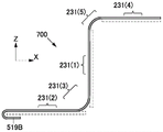
本实施方式中说明的功能面板包括区域231(1)、区域231(2)和区域231(3)(参照图1A至图1C)。The function panel described in this embodiment includes an area 231(1), an area 231(2), and an area 231(3) (refer to FIGS. 1A to 1C ).
《区域231(3)的结构例子1》"Example 1 of the Structure of Area 231(3)"
区域231(3)被夹在区域231(1)与区域231(2)之间(参照图1B及图2A)。另外,区域231(3)可以弯曲。Region 231(3) is sandwiched between region 231(1) and region 231(2) (see FIGS. 1B and 2A ). Additionally, region 231(3) may be curved.
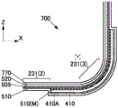
区域231(3)包括功能层520、接合层505及导电膜510M(参照图2B)。The region 231(3) includes the
[接合层505的结构例子][Configuration example of the bonding layer 505]
接合层505具有夹在功能层520与导电膜510M之间的区域。例如,接合层505具有贴合功能层520与导电膜510M的功能。具体而言,可以将功能层520与预先形成在其他基材上的导电膜510M利用接合层505进行贴合。The
可以将无机材料、有机材料或者无机材料和有机材料的复合材料等用于接合层505。An inorganic material, an organic material, a composite material of an inorganic material and an organic material, or the like can be used for the
例如,可以将热熔性树脂或固化树脂等有机材料用于接合层505。For example, an organic material such as a hot-melt resin or a cured resin can be used for the
例如,可以将反应固化型粘合剂、光固化型粘合剂、热固化型粘合剂或/及厌氧型粘合剂等有机材料用于接合层505。For example, an organic material such as a reaction-curable adhesive, a photo-curable adhesive, a heat-curable adhesive, or/and an anaerobic adhesive can be used for the
具体而言,可以将包含环氧树脂、丙烯酸树脂、硅酮树脂、酚醛树脂、聚酰亚胺树脂、亚胺树脂、PVC(聚氯乙烯)树脂、PVB(聚乙烯醇缩丁醛)树脂、EVA(乙烯-醋酸乙烯酯)树脂等的粘合剂用于接合层505。Specifically, epoxy resin, acrylic resin, silicone resin, phenolic resin, polyimide resin, imine resin, PVC (polyvinyl chloride) resin, PVB (polyvinyl butyral) resin, An adhesive such as EVA (ethylene-vinyl acetate) resin is used for the
《功能层520的结构例子1》"Configuration Example 1 of the
功能层520包括电路530及绝缘膜501C。The
《电路530的结构例子1》"Configuration Example 1 of
电路530包括导电膜524(1)。例如,可以将晶体管用于电路530。另外,晶体管的栅电极、源电极或漏电极可以使用导电膜。具体而言,栅电极可以使用导电膜524(1)。
《绝缘膜501C的结构例子1》<<Structure Example 1 of Insulating
绝缘膜501C包括夹在导电膜510M与导电膜524(1)之间的区域。例如,可以将含有硅及氧的材料或聚酰亚胺等用于绝缘膜501C。由此,例如,可以防止电路530与导电膜510M间短路。The insulating
《导电膜510M的结构例子1》<<Structure Example 1 of
导电膜510M与导电膜524(1)间形成电容CS。例如,可以将无机导电性材料、有机导电性材料、金属或导电性陶瓷等用于导电膜510M。具体而言,可以使用铝或钛等可以用于布线的材料。另外,可以利用蒸镀法或印刷法将其形成为膜状。A capacitor CS is formed between the
由此,可以利用导电膜510M使电路530免受噪声影响。其结果,可以提供一种方便性、实用性或可靠性优异的新颖的功能面板。Thereby, the
<功能面板700的结构例子2><Configuration Example 2 of
另外,本发明的一个方式的功能面板700包括基材510。In addition, the
《基材510的结构例子1》"Example 1 of the structure of the
基材510包括与接合层505间夹有导电膜510M的区域。例如,可以将具有柔性的材料用于基材510。The
由此,可以利用基材510保护导电膜510M免受外力等的影响。或者,可以保护导电膜510M免受因弯曲造成的摩擦。其结果,可以提供一种方便性、实用性或可靠性优异的新颖的功能面板。Thereby, the
<功能面板700的结构例子3><Configuration Example 3 of
另外,本发明的一个方式的功能面板700包括区域231(4)和区域231(5)。Further, the
《区域231(5)的结构例子1》"Example 1 of the structure of area 231(5)"
区域231(5)被夹在区域231(1)与区域231(4)间(参照图1A、图1B及图2A)。Region 231(5) is sandwiched between region 231(1) and region 231(4) (see FIGS. 1A, 1B and 2A).
区域231(5)具有抗弯刚度EI(5)。Region 231(5) has flexural stiffness EI(5).
《区域231(3)的结构例子2》"Example 2 of the Structure of Area 231(3)"
区域231(3)包括基材410,基材410具有在与接合层505间夹有导电膜510M的区域(参照图2B、图4A及图30)。例如,可以以接合层410A贴合基材410及基材510。The region 231 ( 3 ) includes the
另外,区域231(3)也可以具有在导电膜510M与基材510间夹有基材410的区域(参照图4B或图4C)。In addition, the region 231 ( 3 ) may have a region in which the
区域231(3)具有抗弯刚度EI(3),抗弯刚度EI(3)比抗弯刚度EI(5)高。Region 231(3) has a flexural stiffness EI(3) that is higher than flexural stiffness EI(5).
由此,可以使区域231(3)的中性面靠近基材410。或者,可以使区域231(5)的中性面比区域231(3)的中性面更靠近基材410。或者,可以以出现在弯曲处的曲率圆的中心为基准以导电膜510M位于功能层520外侧的方式使区域231(3)弯曲。或者,例如可以减轻因向该方向的弯曲施加到导电膜524(1)的拉伸应力。或者,例如,可以将因向该方向的弯曲产生的压缩应力施加到导电膜524(1)上。或者,可以防止因向该方向的弯曲引起功能层520破损。其结果,可以提供一种方便性、实用性或可靠性优异的新颖的功能面板。Thereby, the neutral plane of the region 231 ( 3 ) can be brought close to the
《区域231的结构例子1》"
区域231(3)以出现在弯曲处的曲率圆的中心为基准以导电膜510M位于功能层520外侧的方式弯曲。另外,区域231(5)可以向与区域231(3)相反的方向弯曲(参照图2A、图2B及图3)。The region 231 ( 3 ) is bent so that the
由此,可以使区域231(3)与区域231(5)朝不同方向弯曲。或者,例如可以使功能面板以锯齿形弯曲。或者,例如可以防止因锯齿形弯曲造成功能层520破损。或者,例如,可以以出现在弯曲处的曲率圆的中心为基准以导电膜510M位于功能层520内侧的方式使区域231(5)弯曲。其结果,可以提供一种方便性、实用性或可靠性优异的新颖的功能面板。Thereby, the region 231(3) and the region 231(5) can be bent in different directions. Alternatively, for example, the functional panel can be bent in a zigzag shape. Alternatively, for example, breakage of the
<功能面板700的结构例子4><Configuration Example 4 of
另外,本发明的一个方式的功能面板700包括像素702G(i,j)。注意,功能面板700包括像素703(i,j),像素703(i,j)包括像素702G(i,j)(参照图1A、图8A及图8B)。In addition, the
电路530包括像素电路530G(i,j)(参照图12)。The
《像素702G(i,j)的结构例子1》"Example 1 of the structure of the
像素702G(i,j)包括发光元件550G(i,j)及像素电路530G(i,j)。
发光元件550G(i,j)与像素电路530G(i,j)电连接。The light-emitting
由此,可以利用导电膜510M遮蔽像素702G(i,j)防止噪声传播。可以减轻噪声对显示的影响。或者,可以减轻因弯曲造成的显示失真。或者,可以减轻因手指等的近接造成的显示失真。其结果,可以提供一种方便性、实用性或可靠性优异的新颖的功能面板。Thereby, the
注意,本实施方式可以与本说明书所示的其他实施方式适当地组合。Note that this embodiment mode can be appropriately combined with other embodiments shown in this specification.
实施方式2
在本实施方式中,参照图8A至图11对本发明的一个方式的功能面板的结构进行说明。In the present embodiment, the configuration of a functional panel according to one embodiment of the present invention will be described with reference to FIGS. 8A to 11 .
图8A及图8B是说明本发明的一个方式的功能面板的结构的图。图8A是说明本发明的一个方式的功能面板的结构的俯视图,图8B是说明图8A的一部分的图。8A and 8B are diagrams illustrating the configuration of a functional panel according to an embodiment of the present invention. 8A is a plan view illustrating the structure of a functional panel according to an embodiment of the present invention, and FIG. 8B is a view illustrating a part of FIG. 8A .
图9A是说明图8A的一部分的图,图9B是说明图9A的一部分的图,图9C是说明图9A的其他的一部分的图。9A is a diagram illustrating a part of FIG. 8A , FIG. 9B is a diagram illustrating a part of FIG. 9A , and FIG. 9C is a diagram illustrating another part of FIG. 9A .
图10是说明本发明的一个方式的功能面板的结构的图。图10是说明像素电路的结构的电路图。FIG. 10 is a diagram illustrating a configuration of a functional panel according to an embodiment of the present invention. FIG. 10 is a circuit diagram illustrating a configuration of a pixel circuit.
图11是说明本发明的一个方式的功能面板的结构的图。图11是说明本发明的一个方式的功能面板的像素电路的结构的电路图。FIG. 11 is a diagram illustrating a configuration of a functional panel according to an embodiment of the present invention. 11 is a circuit diagram illustrating a configuration of a pixel circuit of a functional panel according to an embodiment of the present invention.
<功能面板700的结构例子1><Configuration Example 1 of
功能面板700包括一组像素703(i,j)(参照图8A)。The
《像素703(i,j)的结构例子1》"Configuration Example 1 of Pixel 703 (i, j)"
一组像素703(i,j)包括像素702G(i,j)(参照图8B)。像素702G(i,j)包括像素电路530G(i,j)及发光元件550G(i,j),发光元件550G(i,j)与像素电路530G(i,j)电连接(参照图9A)。A set of pixels 703(i,j) includes
《像素电路530G(i,j)的结构例子1》"Configuration Example 1 of the
像素电路530G(i,j)包括开关SW21、开关SW22、晶体管M21、电容器C21及节点N21(参照图10)。The
晶体管M21包括与节点N21电连接的栅电极、与发光元件550G(i,j)电连接的第一电极、与导电膜ANO电连接的第二电极。The transistor M21 includes a gate electrode electrically connected to the node N21, a first electrode electrically connected to the
开关SW21具有根据与节点N21电连接的第一端子、与导电膜S1g(j)电连接的第二端子、导电膜G1(i)的电位控制导通状态或非导通状态的功能。The switch SW21 has a function of controlling a conduction state or a non-conduction state according to a first terminal electrically connected to the node N21, a second terminal electrically connected to the conductive film S1g(j), and the potential of the conductive film G1(i).
开关SW22具有根据与导电膜S2g(j)电连接的第一端子、导电膜G2(i)的电位控制导通状态或非导通状态的功能。The switch SW22 has a function of controlling the conduction state or the non-conduction state according to the potential of the first terminal electrically connected to the conductive film S2g(j) and the conductive film G2(i).
电容器C21包括与节点N21电连接的导电膜、与开关SW22的第二电极电连接的导电膜。The capacitor C21 includes a conductive film electrically connected to the node N21, and a conductive film electrically connected to the second electrode of the switch SW22.
由此,可以将图像信号储存在节点N21中。另外,可以使用开关SW22改变节点N21的电位。另外,可以使用节点N21的电位控制从发光元件550G(i,j)发射的光的强度。其结果是,可以提供一种方便性、实用性或可靠性优异的新颖的功能面板。Thereby, the image signal can be stored in the node N21. In addition, the potential of the node N21 can be changed using the switch SW22. In addition, the intensity of light emitted from the
《发光元件550G(i,j)的结构例子1》"Example 1 of the structure of the light-emitting
例如,可以将有机电致发光元件、无机电致发光元件、发光二极管或QDLED(Quantum Dot LED:量子点发光二极管)等用于发光元件550G(i,j)。For example, an organic electroluminescence element, an inorganic electroluminescence element, a light emitting diode, a QDLED (Quantum Dot LED), or the like can be used for the
《像素703(i,j)的结构例子2》"Configuration Example 2 of Pixel 703 (i, j)"
像素703(i,j)包括像素702S(i,j)(参照图8B)。像素702S(i,j)包括像素电路530S(i,j)及光电转换元件PD(i,j),光电转换元件PD(i,j)与像素电路530S(i,j)电连接(参照图9A)。The pixel 703(i,j) includes the
《像素电路530S(i,j)的结构例子1》"Configuration Example 1 of the
像素电路530S(i,j)包括开关SW31、开关SW32、开关SW33、晶体管M31、电容器C31及节点FD(参照图11)。The
开关SW31具有根据与光电转换元件PD(i,j)电连接的第一端子、与节点FD电连接的第二端子、导电膜TX(i)的电位控制导通状态或非导通状态的功能。The switch SW31 has a function of controlling the conduction state or the non-conduction state according to the first terminal electrically connected to the photoelectric conversion element PD(i,j), the second terminal electrically connected to the node FD, and the potential of the conductive film TX(i). .
开关SW32具有根据与节点FD电连接的第一端子、与导电膜VR电连接的第二端子、导电膜RS(i)的电位控制导通状态或非导通状态的功能。The switch SW32 has a function of controlling a conduction state or a non-conduction state according to a first terminal electrically connected to the node FD, a second terminal electrically connected to the conductive film VR, and the potential of the conductive film RS(i).
电容器C31包括与节点FD电连接的导电膜、与导电膜VCP电连接的导电膜。The capacitor C31 includes a conductive film electrically connected to the node FD, and a conductive film electrically connected to the conductive film VCP.
晶体管M31包括与节点FD电连接的栅电极、与导电膜VPI电连接的第一电极。The transistor M31 includes a gate electrode electrically connected to the node FD, and a first electrode electrically connected to the conductive film VPI.
开关SW33具有根据与晶体管M31的第二电极电连接的第一端子、与导电膜WX(j)电连接的第二端子、导电膜SE(i)的电位控制导通状态或非导通状态的功能。The switch SW33 has a first terminal that is electrically connected to the second electrode of the transistor M31, a second terminal that is electrically connected to the conductive film WX(j), and that controls the conduction state or non-conduction state according to the potential of the conductive film SE(i). Function.
由此,可以使用开关SW31将光电转换元件PD(i,j)所生成的摄像信号传送到节点FD。另外,可以使用开关SW31将光电转换元件PD(i,j)所生成的摄像信号储存在节点FD中。另外,可以使用开关SW31使像素电路530S(i,j)与光电转换元件PD(i,j)之间处于非导通状态。另外,可以使用相关双采样法。另外,可以降低包括在摄像信号中的杂音。其结果是,可以提供一种方便性、实用性或可靠性优异的新颖的功能面板。Thereby, the image pickup signal generated by the photoelectric conversion element PD(i,j) can be transferred to the node FD using the switch SW31. In addition, the image pickup signal generated by the photoelectric conversion element PD(i, j) can be stored in the node FD using the switch SW31. In addition, the switch SW31 can be used to make a non-conduction state between the
《光电转换元件PD(i,j)的结构例子1》<<Structure Example 1 of Photoelectric Conversion Element PD(i, j)>>
例如,可以将异质结型光电转换元件、本体异质结型光电转换元件等用于光电转换元件PD(i,j)。For example, a heterojunction type photoelectric conversion element, a bulk heterojunction type photoelectric conversion element, or the like can be used for the photoelectric conversion element PD(i,j).
《像素703(i,j)的结构例子3》"Configuration Example 3 of Pixel 703 (i, j)"
可以将多个像素用于像素703(i,j)。例如,可以使用显示色相不同的颜色的多个像素。注意,可以将多个像素的每一个换称为子像素。另外,可以以多个子像素为一组而将其换称为像素。Multiple pixels may be used for pixel 703(i,j). For example, a plurality of pixels displaying colors with different hues may be used. Note that each of the plurality of pixels may be interchangeably referred to as a sub-pixel. In addition, a plurality of sub-pixels may be referred to as a group and referred to as a pixel.
由此,可以对该多个像素所显示的颜色进行加法混色或减法混色。另外,可以显示用各个像素不能显示的色相的颜色。Thereby, additive color mixing or subtractive color mixing can be performed on the colors displayed by the plurality of pixels. In addition, colors of hues that cannot be displayed with individual pixels can be displayed.
具体而言,可以将显示蓝色的像素702B(i,j)、显示绿色的像素702G(i,j)及显示红色的像素702R(i,j)用于像素703(i,j)。此外,可以将像素702B(i,j)、像素702G(i,j)及像素702R(i,j)的每一个换称为子像素(参照图8B)。Specifically, the
此外,例如,可以对上述一组追加显示白色等的像素等而将其用于像素703(i,j)。此外,可以将显示青色的像素、显示品红色的像素及显示黄色的子像素用于像素703(i,j)。In addition, for example, a pixel or the like that displays white or the like may be added to the above-mentioned group and used for the pixel 703(i, j). In addition, a cyan-displaying pixel, a magenta-displaying pixel, and a yellow-displaying sub-pixel may be used for the pixel 703(i,j).
例如,可以对上述一组追加发射红外线的像素而将其用于像素703(i,j)。具体而言,可以将发射包含具有650nm以上且1000nm以下的波长的光的光的像素用于像素703(i,j)。For example, an infrared-emitting pixel may be added to the above-mentioned group and used for the pixel 703(i, j). Specifically, a pixel that emits light including light having a wavelength of 650 nm or more and 1000 nm or less can be used for the pixels 703 (i, j).
注意,本实施方式可以与本说明书所示的其他实施方式适当地组合。Note that this embodiment mode can be appropriately combined with other embodiments shown in this specification.
实施方式3
在本实施方式中,参照图12至图15B对本发明的一个方式的功能面板的结构进行说明。In the present embodiment, the configuration of a functional panel according to one embodiment of the present invention will be described with reference to FIGS. 12 to 15B .
图12是说明本发明的一个方式的功能面板的结构的图。图12是沿着图8A的截断线X1-X2、X3-X4、X9-X10、X11-X12及像素的截面图。FIG. 12 is a diagram illustrating a configuration of a functional panel according to an embodiment of the present invention. FIG. 12 is a cross-sectional view of the pixel along the truncation lines X1 - X2 , X3 - X4 , X9 - X10 , X11 - X12 of FIG. 8A .
图13A及图13B是说明本发明的一个方式的功能面板的结构的图。图13A是图8B所示的像素702G(i,j)的截面图。图13B是说明图13A的一部分的截面图。13A and 13B are diagrams illustrating the configuration of a functional panel according to one embodiment of the present invention. FIG. 13A is a cross-sectional view of the
图14A及图14B是说明本发明的一个方式的功能面板的结构的图。图14A是图8B所示的像素702S(i,j)的截面图。图14B是说明图14A的一部分的截面图。14A and 14B are diagrams illustrating the configuration of a functional panel according to one embodiment of the present invention. FIG. 14A is a cross-sectional view of the
图15A及图15B是说明本发明的一个方式的功能面板的结构的图。图15A是沿着图8A的截断线X1-X2及截断线X3-X4的截面图,图15B是说明图15A的一部分的图。15A and 15B are diagrams illustrating the configuration of a functional panel according to one embodiment of the present invention. FIG. 15A is a cross-sectional view taken along the cutting line X1 - X2 and the cutting line X3 - X4 in FIG. 8A , and FIG. 15B is a view illustrating a part of FIG. 15A .
<功能面板700的结构例子1><Configuration Example 1 of
本发明的一个方式的功能面板包括功能层520(参照图12)。The functional panel of one embodiment of the present invention includes a functional layer 520 (see FIG. 12 ).
《功能层520的结构例子1》"Configuration Example 1 of the
功能层520包括像素电路530G(i,j)(参照图12)。功能层520例如包括用于像素电路530G(i,j)的晶体管M21(参照图10及图13A)。The
功能层520包括开口591G。像素电路530G(i,j)在开口591G中与发光元件550G(i,j)电连接(参照图12及图13A)。此外,功能层520可以包括开口591B。The
《功能层520的结构例子2》"Structure Example 2 of the
功能层520包括像素电路530S(i,j)(参照图12)。功能层520例如包括用于像素电路530S(i,j)的开关SW31的晶体管(参照图12及图14A)。The
功能层520包括开口591S,像素电路530S(i,j)在开口591S中与光电转换元件PD(i,j)电连接(参照图12及图14A)。The
由此,可以在功能层520中形成像素电路530G(i,j)。另外,可以在功能层520中形成像素电路530S(i,j)。另外,例如,可以在形成用于像素电路530G(i,j)的半导体膜的工序中形成用于像素电路530S(i,j)的半导体膜。另外,可以使功能面板的制造工序简化。其结果是,可以提供一种方便性、实用性或可靠性优异的新颖的功能面板。Thereby, the
《功能层520的结构例子3》"Structure Example 3 of the
功能层520包括驱动电路GD(参照图8A及图12)。功能层520例如包括用于驱动电路GD的晶体管MD(参照图12及图15A)。The
功能层520包括驱动电路RD及读出电路RC(参照图12)。The
由此,例如,可以在用于像素电路530G(i,j)的半导体膜的工序中形成用于驱动电路GD的半导体膜。另外,例如,可以在用于像素电路530G(i,j)的半导体膜的工序中形成用于驱动电路RD及读出电路RC的半导体膜。另外,可以使功能面板的制造工序简化。其结果是,可以提供一种方便性、实用性或可靠性优异的新颖的功能面板。Thereby, for example, the semiconductor film for the driver circuit GD can be formed in the process of the semiconductor film for the
《晶体管的结构例子》"An example of the structure of a transistor"
可以将底栅型晶体管或顶栅型晶体管等用于功能层520。具体而言,可以将晶体管用于开关。A bottom-gate transistor, a top-gate transistor, or the like can be used for the
晶体管包括半导体膜508、导电膜504、导电膜512A及导电膜512B(参照图13B)。The transistor includes a
半导体膜508包括与导电膜512A电连接的区域508A及与导电膜512B电连接的区域508B。半导体膜508包括区域508A和区域508B之间的区域508C。The
导电膜504包括与区域508C重叠的区域。导电膜504具有栅电极的功能。The
绝缘膜506包括夹在半导体膜508与导电膜504之间的区域。绝缘膜506具有栅极绝缘膜的功能。The insulating
导电膜512A具有源电极的功能和漏电极的功能中的一个,导电膜512B具有源电极的功能和漏电极的功能中的另一个。The
另外,可以将导电膜524用于晶体管。导电膜524包括在其与导电膜504之间夹着半导体膜508的区域。导电膜524具有第二栅电极的功能。In addition, the
在形成用于像素电路的晶体管的半导体膜的工序中,可以形成用于驱动电路的晶体管的半导体膜。In the process of forming the semiconductor film for the transistor of the pixel circuit, the semiconductor film for the transistor of the driver circuit may be formed.
《半导体膜508的结构例子1》<<Structure Example 1 of
例如,可以将包含第14族元素的半导体用于半导体膜508。具体而言,可以将包含硅的半导体用于半导体膜508。For example, a semiconductor containing a Group 14 element can be used for the
[氢化非晶硅][Hydrogenated amorphous silicon]
例如,可以将氢化非晶硅用于半导体膜508。或者,可以将微晶硅等用于半导体膜508。由此,例如,可以提供与将多晶硅用于半导体膜508的功能面板相比显示不均匀较少的功能面板。或者,容易实现功能面板的大型化。For example, hydrogenated amorphous silicon can be used for the
[多晶硅][polysilicon]
例如,可以将多晶硅用于半导体膜508。由此,例如,可以实现比将氢化非晶硅用于半导体膜508的晶体管高的场效应迁移率。或者,例如,可以实现比将氢化非晶硅用于半导体膜508的晶体管高的驱动能力。或者,例如,可以实现比将氢化非晶硅用于半导体膜508的晶体管高的像素开口率。For example, polysilicon can be used for the
或者,例如,可以实现比将氢化非晶硅用于半导体膜508的晶体管高的可靠性。Alternatively, for example, higher reliability than a transistor using hydrogenated amorphous silicon for the
或者,例如,可以使制造晶体管时需要的温度比使用单晶硅的晶体管低。Alternatively, for example, the temperature required to manufacture the transistor can be made lower than that of a transistor using single crystal silicon.
或者,可以通过同一工序形成用于驱动电路的晶体管的半导体膜及用于像素电路的晶体管的半导体膜。或者,可以在与形成有像素电路的衬底同一衬底上形成驱动电路。或者,可以减少构成电子设备的构件数量。Alternatively, the semiconductor film for the transistor of the driver circuit and the semiconductor film for the transistor of the pixel circuit may be formed through the same process. Alternatively, the driver circuit may be formed on the same substrate as the substrate on which the pixel circuit is formed. Alternatively, the number of components constituting the electronic device can be reduced.
[单晶硅][Monocrystalline silicon]
例如,可以将单晶硅用于半导体膜508。由此,例如,可以实现比将氢化非晶硅用于半导体膜508的功能面板高的清晰度。例如,可以提供与将多晶硅用于半导体膜508的功能面板相比显示不均匀较少的功能面板。或者,例如,可以提供智能眼镜或头戴显示器。For example, single crystal silicon can be used for the
《半导体膜508的结构例子2》<<Structure Example 2 of
例如,可以将金属氧化物用于半导体膜508。由此,与利用将非晶硅用于半导体膜的晶体管的像素电路相比,可以延长像素电路能够保持图像信号的时间。具体而言,可以抑制闪烁的发生,并以低于30Hz、优选为低于1Hz、更优选为低于1次/分的频率供应选择信号。其结果是,可以降低数据处理装置的使用者的眼睛疲劳。另外,可以降低用于驱动的功耗。For example, a metal oxide can be used for the
此外,与利用将非晶硅用于半导体膜的晶体管的像素电路相比,可以延长像素电路能够保持摄像信号的时间。具体而言,可以以低于30Hz、优选为低于1Hz、更优选为低于1次/分的频率供应选择信号。其结果是,可以利用全局快门方式进行拍摄。此外,可以在减少畸变的情况下对移动的被摄体进行拍摄。In addition, compared to a pixel circuit using a transistor using amorphous silicon as a semiconductor film, the time for which the pixel circuit can hold an image pickup signal can be extended. In particular, the selection signal may be supplied at a frequency lower than 30 Hz, preferably lower than 1 Hz, more preferably lower than 1 time per minute. As a result, it is possible to photograph using the global shutter method. In addition, moving subjects can be photographed with reduced distortion.
例如,可以利用使用氧化物半导体的晶体管。具体而言,可以将包含铟的氧化物半导体或包含铟、镓及锌的氧化物半导体用于半导体膜。For example, a transistor using an oxide semiconductor can be used. Specifically, an oxide semiconductor containing indium or an oxide semiconductor containing indium, gallium, and zinc can be used for the semiconductor film.
例如,可以使用关闭状态时的泄漏电流比将非晶硅用于半导体膜的晶体管小的晶体管。具体而言,可以将在半导体膜中使用氧化物半导体的晶体管用于开关等。由此,与将使用非晶硅的晶体管用于开关的电路相比,可以以更长的时间保持浮动节点的电位。For example, a transistor whose leakage current in the off state is smaller than that of a transistor using amorphous silicon for the semiconductor film can be used. Specifically, a transistor using an oxide semiconductor as a semiconductor film can be used for switching or the like. As a result, the potential of the floating node can be maintained for a longer period of time than in a circuit using an amorphous silicon transistor for switching.
例如,可以将包含铟、镓及锌的厚度为25nm的膜用作半导体膜508。For example, a film containing indium, gallium, and zinc with a thickness of 25 nm can be used as the
例如,可以将层叠有包含钽及氮的厚度为10nm的膜以及包含铜的厚度为300nm的膜的导电膜用作导电膜504。此外,包含铜的膜包括在其与绝缘膜506之间夹着包含钽及氮的膜的区域。For example, a conductive film in which a film containing tantalum and nitrogen with a thickness of 10 nm and a film containing copper with a thickness of 300 nm are stacked as the
例如,可以将包含硅及氮的厚度为400nm的膜与包含硅、氧及氮的厚度为200nm的膜的叠层膜用于绝缘膜506。此外,包含硅及氮的膜包括在其与半导体膜508之间夹着包含硅、氧及氮的膜的区域。For example, a laminated film of a film containing silicon and nitrogen with a thickness of 400 nm and a film containing silicon, oxygen and nitrogen with a thickness of 200 nm can be used for the insulating
例如,可以将依次层叠有包含钨的厚度为50nm的膜、包含铝的厚度为400nm的膜、包含钛的厚度为100nm的膜的导电膜用作导电膜512A或导电膜512B。此外,包含钨的膜包括与半导体膜508接触的区域。For example, a conductive film in which a film containing tungsten with a thickness of 50 nm, a film containing aluminum with a thickness of 400 nm, and a film containing titanium with a thickness of 100 nm are stacked in this order as the
这里,例如,可以容易地将作为半导体包含非晶硅的底栅型晶体管的生产线改造成作为半导体包含氧化物半导体的底栅型晶体管的生产线。另外,例如,可以容易地将作为半导体包含多晶硅的顶栅型晶体管的生产线改造成作为半导体包含氧化物半导体的顶栅型晶体管的生产线。上述哪一种改造都可以有效地利用现有的生产线。Here, for example, a production line of bottom gate type transistors containing amorphous silicon as a semiconductor can be easily transformed into a production line of bottom gate type transistors containing an oxide semiconductor as a semiconductor. In addition, for example, a production line of top-gate transistors containing polysilicon as a semiconductor can be easily converted into a production line of top-gate transistors containing an oxide semiconductor as a semiconductor, for example. Either of the above modifications can effectively utilize the existing production line.
由此,可以抑制显示的闪烁。另外,可以降低功耗。或者,可以流畅地显示动作快的动态图像。或者,可以以丰富的灰度级显示照片等。其结果是,可以提供一种方便性、实用性或可靠性优异的新颖的功能面板。Thereby, flickering of the display can be suppressed. In addition, power consumption can be reduced. Alternatively, fast-moving moving images can be displayed smoothly. Alternatively, photos, etc. can be displayed in rich grayscale. As a result, a novel functional panel excellent in convenience, practicality, and reliability can be provided.
《半导体膜508的结构例子3》<<Structure Example 3 of
例如,可以将化合物半导体用于晶体管的半导体。具体而言,可以使用包含砷化镓的半导体。For example, compound semiconductors can be used for semiconductors of transistors. Specifically, a semiconductor containing gallium arsenide can be used.
例如,可以将有机半导体用于晶体管的半导体。具体而言,可以将包含聚并苯类或石墨烯的有机半导体用于半导体膜。For example, organic semiconductors can be used for semiconductors of transistors. Specifically, an organic semiconductor containing polyacenes or graphene can be used for the semiconductor film.
《电容器的结构例子》"Example of Capacitor Structure"
电容器包括一个导电膜、另一个导电膜及绝缘膜。该绝缘膜包括夹在一个导电膜与另一个导电膜之间的区域。The capacitor includes one conductive film, another conductive film, and an insulating film. The insulating film includes a region sandwiched between one conductive film and the other conductive film.
例如,可以将用于晶体管的源电极或漏电极的导电膜、用于栅电极的导电膜、用于栅极绝缘膜的绝缘膜用于电容器。For example, a conductive film for a source electrode or a drain electrode of a transistor, a conductive film for a gate electrode, and an insulating film for a gate insulating film can be used for the capacitor.
《功能层520的结构例子2》"Structure Example 2 of the
功能层520包括绝缘膜521、绝缘膜518、绝缘膜516、绝缘膜506及绝缘膜501C等(参照图13A及图13B)。The
绝缘膜521包括夹在像素电路530G(i,j)与发光元件550G(i,j)之间的区域。The insulating
绝缘膜518包括夹在绝缘膜521与绝缘膜501C之间的区域。The insulating
绝缘膜516包括夹在绝缘膜518与绝缘膜501C之间的区域。The insulating
绝缘膜506包括夹在绝缘膜516与绝缘膜501C之间的区域。The insulating
[绝缘膜521][Insulating film 521]
例如,可以将绝缘性无机材料、绝缘性有机材料或包含无机材料和有机材料的绝缘性复合材料用于绝缘膜521。For example, an insulating inorganic material, an insulating organic material, or an insulating composite material containing an inorganic material and an organic material can be used for the insulating
具体而言,可以将无机氧化物膜、无机氮化物膜、无机氧氮化物膜等或层叠有选自这些膜中的多个膜的叠层材料用于绝缘膜521。Specifically, an inorganic oxide film, an inorganic nitride film, an inorganic oxynitride film, or the like, or a laminate material in which a plurality of films selected from these films are laminated can be used for the insulating
例如,可以将包含氧化硅膜、氮化硅膜、氧氮化硅膜、氧化铝膜等或层叠有选自这些膜中的多个材料的叠层材料的膜用于绝缘膜521。氮化硅膜是致密的膜具有优良的抑制杂质扩散的功能。For example, a film including a silicon oxide film, a silicon nitride film, a silicon oxynitride film, an aluminum oxide film, or the like, or a laminate material in which a plurality of materials selected from these films are laminated can be used for the insulating
例如,可以将聚酯、聚烯烃、聚酰胺、聚酰亚胺、聚碳酸酯、聚硅氧烷或丙烯酸树脂等或选自上述树脂中的多个树脂的叠层材料或复合材料等用于绝缘膜521。聚酰亚胺与其他的有机材料相比具有更好的热稳定性、绝缘性、韧性、低介电常数、低热膨胀率、耐化学品性等特性。由此,尤其优选将聚酰亚胺用于绝缘膜521等。For example, polyester, polyolefin, polyamide, polyimide, polycarbonate, polysiloxane, or acrylic resin or the like, or a laminate or composite material of a plurality of resins selected from the above-mentioned resins can be used for insulating
另外,也可以使用具有感光性的材料形成绝缘膜521。具体而言,可以将采用感光性聚酰亚胺或感光性丙烯酸树脂等形成的膜用于绝缘膜521。In addition, the insulating
由此,例如,通过绝缘膜521可以使起因于与绝缘膜521重叠的各种结构的台阶平坦化。Thereby, for example, steps due to various structures overlapping with the insulating
[绝缘膜518][Insulating film 518]
例如,可以将能够用于绝缘膜521的材料用于绝缘膜518。For example, a material that can be used for the insulating
例如,可以将能够抑制氧、氢、水、碱金属、碱土类金属等扩散的材料用于绝缘膜518。具体而言,可以将氮化物绝缘膜用于绝缘膜518。例如,可以将氮化硅、氮氧化硅、氮化铝、氮氧化铝等用于绝缘膜518。由此,可以防止杂质扩散到晶体管的半导体膜。For example, a material capable of suppressing diffusion of oxygen, hydrogen, water, alkali metals, alkaline earth metals, or the like can be used for the insulating
[绝缘膜516][Insulating film 516]
例如,可以将能够用于绝缘膜521的材料用于绝缘膜516。For example, a material that can be used for the insulating
具体而言,可以将其制造方法与绝缘膜518的制造方法不同的膜用于绝缘膜516。Specifically, a film whose manufacturing method is different from that of the insulating
[绝缘膜506][Insulating film 506]
例如,可以将能够用于绝缘膜521的材料用于绝缘膜506。For example, a material that can be used for the insulating
具体而言,可以将含有氧化硅膜、氧氮化硅膜、氮氧化硅膜、氮化硅膜、氧化铝膜、氧化铪膜、氧化钇膜、氧化锆膜、氧化镓膜、氧化钽膜、氧化镁膜、氧化镧膜、氧化铈膜或氧化钕膜的膜用于绝缘膜506。Specifically, a silicon oxide film, a silicon oxynitride film, a silicon nitride oxide film, a silicon nitride film, an aluminum oxide film, a hafnium oxide film, a yttrium oxide film, a zirconium oxide film, a gallium oxide film, and a tantalum oxide film may be formed. A film of , a magnesium oxide film, a lanthanum oxide film, a cerium oxide film, or a neodymium oxide film is used for the insulating
[绝缘膜501D][Insulating
绝缘膜501D包括夹在绝缘膜501C与绝缘膜516之间的区域。The insulating
例如,可以将能够用于绝缘膜506的材料用于绝缘膜501D。For example, a material that can be used for the insulating
[绝缘膜501C][Insulating
例如,可以将能够用于绝缘膜521的材料用于绝缘膜501C。具体而言,可以将包含硅及氧的材料用于绝缘膜501C。由此,可以抑制杂质扩散到像素电路、发光元件或光电转换元件等。For example, a material that can be used for the insulating
《功能层520的结构例子3》"Structure Example 3 of the
功能层520包括导电膜、布线及端子。可以将具有导电性的材料用于布线、电极、端子、导电膜等。The
[布线等][wiring, etc.]
例如,可以将无机导电材料、有机导电材料、金属或导电性陶瓷等用于布线等。For example, inorganic conductive materials, organic conductive materials, metals, conductive ceramics, or the like can be used for wiring or the like.
具体地,可以将选自铝、金、铂、银、铜、铬、钽、钛、钼、钨、镍、铁、钴、钯或锰的金属元素等用于布线等。或者,可以将含有上述金属元素的合金等用于布线等。尤其是,铜和锰的合金适用于利用湿蚀刻法的微细加工。Specifically, a metal element selected from aluminum, gold, platinum, silver, copper, chromium, tantalum, titanium, molybdenum, tungsten, nickel, iron, cobalt, palladium, or manganese or the like can be used for wiring or the like. Alternatively, an alloy or the like containing the above-mentioned metal elements can be used for wiring or the like. In particular, alloys of copper and manganese are suitable for microfabrication by wet etching.
具体地,布线等可以采用如下结构:在铝膜上层叠有钛膜的双层结构;在氮化钛膜上层叠有钛膜的双层结构;在氮化钛膜上层叠有钨膜的双层结构;在氮化钽膜或氮化钨膜上层叠有钨膜的双层结构;依次层叠有钛膜、铝膜和钛膜的三层结构等。Specifically, the wiring and the like may adopt the following structures: a double-layer structure in which a titanium film is laminated on an aluminum film; a double-layer structure in which a titanium film is laminated on a titanium nitride film; a double-layer structure in which a tungsten film is laminated on the titanium nitride film Layer structure; double-layer structure with tungsten film stacked on tantalum nitride film or tungsten nitride film; triple-layer structure with titanium film, aluminum film and titanium film stacked in sequence, etc.
具体地,可以将氧化铟、铟锡氧化物、铟锌氧化物、氧化锌、添加了镓的氧化锌等导电氧化物用于布线等。Specifically, conductive oxides such as indium oxide, indium tin oxide, indium zinc oxide, zinc oxide, and gallium-added zinc oxide can be used for wiring or the like.
具体地,可以将含有石墨烯或石墨的膜用于布线等。Specifically, a film containing graphene or graphite can be used for wiring or the like.
例如,可以形成含有氧化石墨烯的膜,然后通过使含有氧化石墨烯的膜还原来形成含有石墨烯的膜。作为还原方法,可以举出利用加热的方法以及利用还原剂的方法等。For example, a graphene oxide-containing film may be formed, and then the graphene-containing film may be formed by reducing the graphene oxide-containing film. As a reduction method, the method using a heating, the method using a reducing agent, etc. are mentioned.
例如,可以将包含金属纳米线的膜用于布线等。具体而言,可以使用包含银的金属纳米线。For example, a film containing metal nanowires can be used for wiring or the like. Specifically, metal nanowires containing silver can be used.
具体而言,可以将导电高分子用于布线等。Specifically, a conductive polymer can be used for wiring or the like.
此外,例如可以使用导电材料将端子519B与柔性印刷电路板FPC1电连接(参照图12)。具体而言,例如可以使用导电材料CP将端子519B与柔性印刷电路板FPC1电连接。In addition, the terminal 519B may be electrically connected to the flexible printed circuit board FPC1 using, for example, a conductive material (refer to FIG. 12 ). Specifically, the terminal 519B can be electrically connected to the flexible printed circuit board FPC1 using, for example, the conductive material CP.
<功能面板700的结构例子2><Configuration Example 2 of
另外,功能面板700包括基材510、基材770及密封剂705(参照图13A)。另外,功能面板700可以包括结构体KB。In addition, the
《基材510、基材770》"
可以将具有透光性的材料用于基材510或基材770。A light-transmitting material can be used for the
例如,可以将具有柔性的材料用于基材510或基材770。由此,可以提供具有柔性的功能面板。For example, a material having flexibility may be used for the
例如,可以使用厚度为0.1mm以上且0.7mm以下的材料。具体而言,可以使用抛光至0.1mm左右厚的材料。由此,可以降低重量。For example, a material having a thickness of 0.1 mm or more and 0.7 mm or less can be used. Specifically, a material polished to a thickness of about 0.1 mm can be used. Thereby, the weight can be reduced.
此外,可以将第六世代(1500mm×1850mm)、第七世代(1870mm×2200mm)、第八世代(2200mm×2400mm)、第九世代(2400mm×2800mm)、第十世代(2950mm×3400mm)等玻璃衬底用于基材510或基材770。由此,可以制造大型显示装置。In addition, the sixth generation (1500mm×1850mm), seventh generation (1870mm×2200mm), eighth generation (2200mm×2400mm), ninth generation (2400mm×2800mm), tenth generation (2950mm×3400mm) and other glass can be used A substrate is used for
可以将有机材料、无机材料或混合有机材料和无机材料等的复合材料等用于基材510或基材770。For the
例如,可以使用玻璃、陶瓷、金属等无机材料。具体而言,可以将无碱玻璃、钠钙玻璃、钾钙玻璃、水晶玻璃、铝硅酸玻璃、钢化玻璃、化学钢化玻璃、石英或蓝宝石等用于基材510或基材770。或者,可以将铝硅酸玻璃、钢化玻璃、化学钢化玻璃或蓝宝石等适当地用于功能面板中的配置在靠近使用者的一侧的基材510或基材770。由此,可以防止使用时造成的功能面板的损坏或损伤。For example, inorganic materials such as glass, ceramics, and metals can be used. Specifically, alkali-free glass, soda-lime glass, potassium-lime glass, crystal glass, aluminosilicate glass, tempered glass, chemically tempered glass, quartz, sapphire, or the like can be used for the
具体而言,可以使用无机氧化物膜、无机氮化物膜或无机氧氮化物膜等。例如,可以使用氧化硅膜、氮化硅膜、氧氮化硅膜、氧化铝膜等。可以将不锈钢或铝等用于基材510或基材770。Specifically, an inorganic oxide film, an inorganic nitride film, an inorganic oxynitride film, or the like can be used. For example, a silicon oxide film, a silicon nitride film, a silicon oxynitride film, an aluminum oxide film, or the like can be used. Stainless steel, aluminum, or the like can be used for the
例如,可以将以硅或碳化硅为材料的单晶半导体衬底或多晶半导体衬底、以硅锗等为材料的化合物半导体衬底、SOI衬底等用于基材510或基材770。由此,可以将半导体元件形成于基材510或基材770。For example, a single crystal semiconductor substrate or a polycrystalline semiconductor substrate made of silicon or silicon carbide, a compound semiconductor substrate made of silicon germanium or the like, an SOI substrate, or the like can be used for the
例如,可以将树脂、树脂薄膜或塑料等有机材料用于基材510或基材770。具体而言,可以将包含聚酯、聚烯烃、聚酰胺(尼龙、芳族聚酰胺等)、聚酰亚胺、聚碳酸酯、聚氨酯、丙烯酸树脂、环氧树脂或硅酮等具有硅氧烷键合的树脂的材料用于基材510或基材770。例如,可以使用含有上述树脂的树脂薄膜、树脂板或叠层材料等。由此,可以降低重量。或者,例如,可以降低因掉落导致的损伤等的发生频率。For example, an organic material such as resin, resin film, or plastic can be used for the
具体而言,可以将聚对苯二甲酸乙二醇酯(PET)、聚萘二甲酸乙二醇酯(PEN)、聚醚砜(PES)、环烯烃聚合物(COP)或环烯烃共聚物(COC)等用于基材510或基材770。Specifically, polyethylene terephthalate (PET), polyethylene naphthalate (PEN), polyether sulfone (PES), cyclic olefin polymer (COP) or cyclic olefin copolymer may be (COC) or the like is used for the
例如,可以将金属板、薄板状的玻璃板或无机材料等的膜与树脂薄膜等贴合在一起的复合材料用于基材510或基材770。例如,基材510或基材770可以使用将纤维状或粒子状的金属、玻璃或无机材料等分散到树脂薄膜而得到的复合材料。例如,基材510或基材770可以使用将纤维状或粒子状的树脂或有机材料等分散到无机材料而得到的复合材料。For example, a composite material in which a metal plate, a thin-plate-shaped glass plate, or a film of an inorganic material, etc., and a resin film or the like are bonded together can be used for the
另外,可以将单层的材料或层叠有多个层的材料用于基材510或基材770。例如,可以使用层叠有绝缘膜等的材料。具体而言,可以使用层叠有选自氧化硅层、氮化硅层和氧氮化硅层等中的一种或多种的膜的材料。由此,例如,可以防止包含在基材中的杂质的扩散。或者,可以防止包含在玻璃或树脂中的杂质的扩散。或者,可以防止透过树脂的杂质的扩散。In addition, a single-layer material or a material in which a plurality of layers are laminated may be used for the
另外,可以将纸或木材等用于基材510或基材770。In addition, paper, wood, or the like can be used for the
例如,可以将具有能够承受制造工序中的加热处理的耐热性的材料用于基材510或基材770。具体而言,可以将对在直接形成晶体管或电容器等的制造工序中的加热具有耐性的材料用于基材510或基材770。For example, a material having heat resistance capable of withstanding heat treatment in the manufacturing process may be used for the
例如,可以使用如下方法:例如在对制造工序中的加热具有耐性的工序用衬底上形成绝缘膜、晶体管或电容器等,并将形成了的绝缘膜、晶体管或电容器等转置到基材510或基材770。由此,例如可以在具有柔性的衬底上形成绝缘膜、晶体管或电容器等。For example, a method of forming an insulating film, a transistor, a capacitor, or the like on a process substrate having resistance to heating in a manufacturing process can be used, and transposing the formed insulating film, transistor, capacitor, or the like on the
《密封剂705》"
密封剂705包括夹在功能层520与基材770之间的区域,并具有贴合功能层520与基材770的功能(参照图13A)。The
可以将无机材料、有机材料或无机材料和有机材料的复合材料等用于密封剂705。An inorganic material, an organic material, a composite material of an inorganic material and an organic material, or the like can be used for the
例如,可以将热熔性树脂或固化树脂等有机材料用于密封剂705。For example, an organic material such as a hot-melt resin or a cured resin can be used for the
例如,可以将反应固化型粘合剂、光固化型粘合剂、热固化型粘合剂或/及厌氧型粘合剂等有机材料用于密封剂705。For example, an organic material such as a reaction-curable adhesive, a photo-curable adhesive, a heat-curable adhesive, or/and an anaerobic adhesive can be used for the
具体而言,可以将包含环氧树脂、丙烯酸树脂、硅酮树脂、酚醛树脂、聚酰亚胺树脂、亚胺树脂、PVC(聚氯乙烯)树脂、PVB(聚乙烯醇缩丁醛)树脂、EVA(乙烯-醋酸乙烯酯)树脂等的粘合剂用于密封剂705。Specifically, epoxy resin, acrylic resin, silicone resin, phenolic resin, polyimide resin, imine resin, PVC (polyvinyl chloride) resin, PVB (polyvinyl butyral) resin, An adhesive such as EVA (ethylene vinyl acetate) resin is used for the
《结构体KB》"Structure KB"
结构体KB包括夹在功能层520与基材770之间的区域。此外,结构体KB具有在功能层520与基材770之间设置规定间隔的功能。Structure KB includes a region sandwiched between
注意,本实施方式可以与本说明书所示的其他实施方式适当地组合。Note that this embodiment mode can be appropriately combined with other embodiments shown in this specification.
实施方式4
在本实施方式中,参照图13A至图15B对本发明的一个方式的功能面板的结构进行说明。In the present embodiment, the configuration of a functional panel according to one embodiment of the present invention will be described with reference to FIGS. 13A to 15B .
<功能面板700的结构例子1><Configuration Example 1 of
功能面板700包括发光元件550G(i,j)(参照图13A和图13B)。The
《发光元件550G(i,j)的结构例子2》<<Structure Example 2 of Light-Emitting
可以将电极551G(i,j)、电极552及包含发光性材料的层553G(j)用于发光元件550G(i,j)。此外,包含发光性材料的层553G(j)包括夹在电极551G(i,j)与电极552之间的区域。The
[包含发光性材料的层553G(j)的结构例子1][Structure Example 1 of
例如,可以将叠层材料用于包含发光性材料的层553G(j)。For example, a laminate material can be used for the
例如,可以将发射蓝色光的材料、发射绿色光的材料、发射红色光的材料、发射红外线的材料或发射紫外线的材料用于包含发光性材料的层553G(j)。For example, a blue light emitting material, a green light emitting material, a red light emitting material, an infrared light emitting material, or an ultraviolet light emitting material may be used for the
[包含发光性材料的层553G(j)的结构例子2][Structure Example 2 of
例如,可以将以发射白色光的方式层叠的叠层材料用于包含发光性材料的层553G(j)。For example, a laminate material laminated so as to emit white light can be used for the
具体而言,可以将发射色相不同的光的多个材料用于包含发光性材料的层553G(j)。Specifically, a plurality of materials that emit light of different hues can be used for the
例如,可以将如下叠层材料用于包含发光性材料的层553G(j),其中层叠有具有包含发射蓝色光的荧光材料的发光性材料的层以及具有包含发射绿色光及红色光的荧光材料以外的材料的层。另外,可以将层叠有具有包含发射蓝色光的荧光材料的发光性材料的层以及具有包含发射黄色光的荧光材料以外的材料的层的叠层材料用于包含发光性材料的层553G(j)。For example, for the
注意,例如,包含发光性材料的层553G(j)可以与着色膜重叠而使用。由此,可以从白色光取出规定色相的光。Note that, for example, the
[包含发光性材料的层553G(j)的结构例子3][Structure Example 3 of
例如,可以将以发射蓝色光或紫外线的方式层叠的叠层材料用于包含发光性材料的层553G(j)。此外,例如,包含发光性材料的层553G(j)可以与颜色转换层重叠而使用。For example, a laminate material laminated so as to emit blue light or ultraviolet light can be used for the
[包含发光性材料的层553G(j)的结构例子4][Structure Example 4 of
包含发光性材料的层553G(j)包括发光单元。发光单元包括一个区域,在该区域中从一方注入的电子与从另一方注入的空穴再结合。此外,发光单元包含发光性材料,发光性材料将因电子与空穴的再结合而产生的能量以光的形式放出。注意,可以将空穴传输层及电子传输层用于发光单元。空穴传输层配置得比电子传输层更靠近正极一侧,空穴传输层的空穴迁移率比电子传输层高。The
例如,可以将多个发光单元及中间层用于包含发光性材料的层553G(j)。中间层具有被夹在两个发光单元间的区域。中间层具有电荷产生区域,中间层能够对配置于阴极一侧的发光单元供应空穴并对配置于阳极一侧的发光单元供应电子。注意,有时将具有多个发光单元及中间层的结构称为串联型发光元件。For example, a plurality of light-emitting units and intermediate layers may be used for the
由此,可以提高发光的电流效率。或者,可以在相同的亮度下降低在发光元件中流过的电流的密度。或者,可以提高发光元件的可靠性。Thereby, the current efficiency of light emission can be improved. Alternatively, the density of the current flowing through the light-emitting element can be reduced at the same luminance. Alternatively, the reliability of the light-emitting element can be improved.
例如,可以层叠包含发射一个色相的光的材料的发光单元及包含发射其他色相的光的材料的发光单元而将其用于包含发光性材料的层553G(j)。或者,可以层叠包含发射一个色相的光的材料的发光单元及包含发射同一色相的光的材料的发光单元而将其用于包含发光性材料的层553G(j)。具体而言,可以层叠包含发射蓝色光的材料的两个发光单元而使用。For example, a light-emitting unit including a material emitting light of one hue and a light-emitting unit including a material emitting light of another hue may be stacked and used for the
此外,例如,可以将高分子化合物(低聚物、树枝状聚合物、聚合物等)、中分子化合物(介于低分子与高分子之间的化合物:分子量为400以上且4000以下)等用于含有发光性材料的层553G(j)。In addition, for example, high molecular compounds (oligomers, dendrimers, polymers, etc.), medium molecular weight compounds (compounds between low molecules and high polymers: molecular weight of 400 or more and 4000 or less) and the like can be used for in the
[电极551G(i,j)、电极552][
例如,可以将能够用于布线等的材料用于电极551G(i,j)或电极552。具体而言,可以将对可见光具有透光性的材料用于电极551G(i,j)或电极552。For example, a material that can be used for wiring or the like can be used for the
例如,可以使用导电性氧化物或含有铟的导电性氧化物、氧化铟、铟锡氧化物、铟锌氧化物、氧化锌、添加有镓的氧化锌等。或者,可以使用薄得能够使光透过的金属膜。或者,可以使用对可见光具有透光性的材料。For example, conductive oxides or conductive oxides containing indium, indium oxide, indium tin oxide, indium zinc oxide, zinc oxide, gallium-added zinc oxide, or the like can be used. Alternatively, a metal film thin enough to transmit light may be used. Alternatively, a material translucent to visible light may be used.
例如,可以将使光的一部分透过并反射光的其他部分的金属膜用于电极551G(i,j)或电极552。例如,通过使用包含发光性材料的层553G(j)等,调整电极551G(i,j)与电极552之间的距离。For example, a metal film that transmits a part of the light and reflects the other part of the light may be used for the
由此,可以使发光元件550G(i,j)具有微小共振器结构。或者,与其他的光相比可以更有效地取出指定波长的光。或者,可以取出光谱的半宽窄的光。或者,可以取出鲜明的颜色的光。Thereby, the light-emitting
例如,可以将高效地反射光的膜用于电极551G(i,j)或电极552。具体而言,可以将包含银及钯等的材料或包含银及铜等的材料用于金属膜。For example, a film that reflects light efficiently can be used for the
电极551G(i,j)在开口591G中与像素电路530G(i,j)电连接(参照图14A)。电极551G(i,j)例如与形成在绝缘膜528中的开口重叠,电极551G(i,j)的边缘设置有绝缘膜528。The
由此,可以防止电极551G(i,j)及电极552的短路。Thereby, the short circuit of the
《光电转换元件PD(i,j)的结构例子2》<<Structure Example 2 of Photoelectric Conversion Element PD(i, j)>>
光电转换元件PD(i,j)包括电极551S(i,j)、电极552及包含光电转换材料的层553S(j)(参照图14A)。The photoelectric conversion element PD(i,j) includes an
例如,可以将异质结型光电转换元件、本体异质结型光电转换元件等用于光电转换元件PD(i,j)。For example, a heterojunction type photoelectric conversion element, a bulk heterojunction type photoelectric conversion element, or the like can be used for the photoelectric conversion element PD(i,j).
[包含光电转换材料的层553S(j)的结构例子1][Structure Example 1 of
例如,可以将以p型半导体膜及n型半导体膜互相接触的方式层叠的叠层膜用于包含光电转换材料的层553S(j)。注意,可以将在包含光电转换材料的层553S(j)中使用这种结构的叠层膜的光电转换元件PD(i,j)称为PN型光电二极管。For example, a laminated film in which the p-type semiconductor film and the n-type semiconductor film are stacked so that the p-type semiconductor film and the n-type semiconductor film are in contact with each other can be used for the
例如,可以将以在p型半导体膜与n型半导体膜之间夹有i型半导体膜的方式层叠p型半导体膜、i型半导体膜及n型半导体膜的叠层膜用于包含光电转换材料的层553S(j)。注意,可以将在包含光电转换材料的层553S(j)中使用这种结构的叠层膜的光电转换元件PD(i,j)称为PIN型光电二极管。For example, a laminated film in which a p-type semiconductor film, an i-type semiconductor film, and an n-type semiconductor film are stacked such that an i-type semiconductor film is sandwiched between a p-type semiconductor film and an n-type semiconductor film can be used for the photoelectric conversion material.
例如,可以将叠层膜用于包含光电转换材料的层553S(j),该叠层膜是在p+型半导体膜与n型半导体膜之间夹有p-型半导体膜且在该p-型半导体膜与该n型半导体膜之间夹有p型半导体膜的方式层叠p+型半导体膜、p-型半导体膜、p型半导体膜及n型半导体膜而成的。注意,可以将在包含光电转换材料的层553S(j)中使用这种结构的叠层膜的光电转换元件PD(i,j)称为雪崩光电二极管。For example, for the
[包含光电转换材料的层553S(j)的结构例子2][Structure example 2 of
例如,可以将包含第14族元素的半导体用于包含光电转换材料的层553S(j)。具体而言,可以将包含硅的半导体用于包含光电转换材料的层553S(j)。例如,可以将氢化非晶硅、微晶硅、多晶硅或单晶硅等用于包含光电转换材料的层553S(j)。For example, a semiconductor containing a Group 14 element can be used for the
例如,可以将有机半导体用于包含光电转换材料的层553S(j)。具体而言,可以将用于包含发光性材料的层553G(j)的层的一部分用于包含光电转换材料的层553S(j)的一部分。For example, an organic semiconductor can be used for the
具体而言,可以将用作包含发光性材料的层553G(j)的空穴传输层用作包含光电转换材料的层553S(j)。或者,可以将用作包含发光性材料的层553G(j)的电子传输层用作包含光电转换材料的层553S(j)。或者,可以将空穴传输层及电子传输层用作包含光电转换材料的层553S(j)。由此,可以在形成用作包含发光性材料的层553G(j)的空穴传输层的工序中形成用作包含光电转换材料的层553S(j)的空穴传输层。或者,可以在形成用作包含发光性材料的层553G(j)的电子传输层的工序中形成用作包含光电转换材料的层553S(j)的电子传输层。或者,可以简化制造工序。Specifically, the hole transport layer used as the
此外,例如,可以将富勒烯(例如C60、C70等)或其衍生物等具有电子接收性的有机半导体材料用于n型半导体膜。In addition, for example, an organic semiconductor material having electron accepting properties such as fullerene (eg, C 60 , C 70 , etc.) or a derivative thereof can be used for the n-type semiconductor film.
例如,可以将铜(II)酞菁(Copper(II)phthalocyanine:CuPc)、四苯基二苯并二茚并芘(Tetraphenyldibenzoperiflanthene:DBP)等具有电子施主性的有机半导体材料用于p型半导体膜。For example, organic semiconductor materials having electron-donating properties such as copper(II) phthalocyanine (CuPc) and tetraphenyldibenzoperiflanthene (DBP) can be used for the p-type semiconductor film .
例如,可以将共蒸镀具有电子接收性的半导体材料及具有电子施主性的半导体材料而成的膜用于i型半导体膜。For example, a film in which an electron-accepting semiconductor material and an electron-donating semiconductor material are co-evaporated can be used for the i-type semiconductor film.
<功能面板700的结构例子2><Configuration Example 2 of
功能面板700包括绝缘膜528及绝缘膜573(参照图13A)。The
《绝缘膜528》《Insulating
绝缘膜528包括夹在功能层520与基材770之间的区域,绝缘膜528在与发光元件550G(i,j)重叠的区域包括开口(参照图13A)。The insulating
例如,可以将能够用于绝缘膜521的材料用于绝缘膜528。具体而言,可以将氧化硅膜、包含丙烯酸树脂的膜或包含聚酰亚胺的膜等用于绝缘膜528。For example, a material that can be used for the insulating
《绝缘膜573》《Insulating Film 573》
绝缘膜573包括功能层520与绝缘膜573之间夹有发光元件550G(i,j)的区域(参照图13A)。The insulating film 573 includes a region where the light-emitting
例如,可以将一个膜或层叠多个膜的叠层膜用于绝缘膜573。具体而言,可以将层叠使用不容易损伤发光元件550G(i,j)的方法形成的绝缘膜573A与缺陷少且致密的绝缘膜573B的叠层膜用于绝缘膜573。For example, one film or a laminated film in which a plurality of films are laminated can be used for the insulating film 573 . Specifically, a laminated film in which an insulating
由此,可以抑制杂质扩散到发光元件550G(i,j)。或者,可以提高发光元件550G(i,j)的可靠性。Thereby, diffusion of impurities to the light-emitting
<功能面板700的结构例子3><Configuration Example 3 of
功能面板700包括功能层720(参照图13A)。The
《功能层720》"
功能层720包括遮光膜BM、着色膜CF(G)及绝缘膜771。另外,也可以使用颜色转换层。The
《遮光膜BM》《Shading Film BM》
遮光膜BM在与像素702G(i,j)重叠的区域包括开口。另外,遮光膜BM在与像素702S(i,j)重叠的区域包括开口。The light shielding film BM includes openings in regions overlapping with the
例如,可以将暗色材料用于遮光膜BM。由此,可以提高显示的对比度。For example, a dark-colored material can be used for the light shielding film BM. Thereby, the contrast ratio of the display can be improved.
《着色膜CF(G)》《Coloring Film CF(G)》
着色膜CF(G)包括夹在基材770与发光元件550G(i,j)之间的区域。例如,可以将使指定颜色的光选择性地透过的材料用于着色膜CF(G)。具体而言,可以将使红色光、绿色光或蓝色光透过的材料用于着色膜CF(G)。The colored film CF(G) includes a region sandwiched between the
《绝缘膜771的结构例子》<<Structure Example of Insulating
绝缘膜771包括夹在基材770与发光元件550G(i,j)之间的区域。The insulating
绝缘膜771包括与基材770间夹有遮光膜BM、着色膜CF(G)或颜色转换层的区域。由此,可以使起因于遮光膜BM、着色膜CF(G)或颜色色转换层的厚度的凹凸平坦。The insulating
《颜色转换层》"Color Conversion Layer"
颜色转换层包括夹在基材770与发光元件550G(i,j)之间的区域。The color conversion layer includes a region sandwiched between
例如,可以将发射具有其波长比所入射的光的波长长的光的材料用于颜色转换层。例如,可以将吸收蓝色光或紫外线而转换为绿色光发射的材料、吸收蓝色光或紫外线而转换为红色光发射的材料或者吸收紫外线而转换为蓝色光发射的材料用于颜色转换层。具体而言,可以将直径几nm的量子点用于颜色转换层。由此,可以发射具有半宽窄的光谱的光。或者,可以发射彩度高的光。For example, a material that emits light having a wavelength longer than that of incident light can be used for the color conversion layer. For example, a material that absorbs blue or ultraviolet light and converts to green light emission, a material that absorbs blue or ultraviolet light and converts to red light emission, or a material that absorbs ultraviolet light and converts to blue light emission can be used for the color conversion layer. Specifically, quantum dots with a diameter of several nm can be used for the color conversion layer. Thereby, light having a spectrum with a narrow half width can be emitted. Alternatively, light with high chroma may be emitted.
<功能面板700的结构例子4><Configuration Example 4 of
功能面板700包括遮光膜KBM(参照图13A)。The
《遮光膜KBM》《Shading Film KBM》
遮光膜KBM在与像素702S(i,j)重叠的区域包括开口。此外,遮光膜KBM包括夹在功能层520与基材770之间的区域并具有在功能层520与基材770之间设置指定的空隙的功能。例如,可以将暗色材料用于遮光膜KBM。由此,可以抑制进入到像素702S(i,j)的杂散光。The light shielding film KBM includes openings in regions overlapping with the
<功能面板700的结构例子5><Configuration Example 5 of
功能面板700包括功能膜770P等(参照图13A)。The
《功能膜770P等》"
功能膜770P包括与发光元件550G(i,j)重叠的区域。The
例如,可以将防反射膜、偏振膜、相位差膜、光扩散膜或聚光膜等用作功能膜770P。For example, an antireflection film, a polarizing film, a retardation film, a light diffusing film, a light condensing film, or the like can be used as the
例如,可以将厚度为1μm以下的抗反射膜用于功能膜770P。具体而言,可以将层叠3层以上,优选层叠5层以上,更优选层叠15层以上的介电质的叠层膜用于功能膜770P。由此,可以将反射率抑制为0.5%以下,优选为0.08%以下。For example, an antireflection film having a thickness of 1 μm or less can be used for the
例如,可以将圆偏振膜用于功能膜770P。For example, a circular polarizing film can be used for the
另外,可以将抑制尘埃的附着的抗静电膜、不易附着污垢的防水膜、不易附着污垢的放油膜、抗反射膜(antireflection film)、防眩光膜(non-glare film)、抑制使用时的损伤的硬涂膜、能够修复所产生的损伤的自修复性膜等用于功能膜770P。In addition, an antistatic film that suppresses the adhesion of dust, a waterproof film that does not easily adhere to dirt, an oil release film that does not easily adhere to dirt, an antireflection film, an anti-glare film, and a damage during use can be used. A hard coat film, a self-healing film capable of repairing the resulting damage, etc. are used for the
注意,本实施方式可以与本说明书所示的其他实施方式适当地组合。Note that this embodiment mode can be appropriately combined with other embodiments shown in this specification.
实施方式5
在本实施方式中,参照图16至图18对本发明的一个方式的功能面板的结构进行说明。In the present embodiment, the configuration of a functional panel according to one embodiment of the present invention will be described with reference to FIGS. 16 to 18 .
图16是说明本发明的一个方式的功能面板的结构的图。FIG. 16 is a diagram illustrating a configuration of a function panel according to an embodiment of the present invention.
图17A及图17B是说明本发明的一个方式的功能面板的结构的电路图。图17A是说明能够用于本发明的一个方式的功能面板的放大电路的一部分的电路图,图17B是说明能够用于本发明的一个方式的功能面板的采样电路的一部分的电路图。17A and 17B are circuit diagrams illustrating the configuration of a functional panel according to one embodiment of the present invention. 17A is a circuit diagram illustrating a part of an amplifier circuit that can be used in the functional panel of one embodiment of the present invention, and FIG. 17B is a circuit diagram illustrating a part of a sampling circuit that can be used in the functional panel of one embodiment of the present invention.
图18是说明本发明的一个方式的功能面板的工作的图。FIG. 18 is a diagram illustrating the operation of the function panel according to one embodiment of the present invention.
<功能面板700的结构例子1><Configuration Example 1 of
在本实施方式中说明的功能面板700包括区域231(参照图16)。The
《区域231的结构例子1》"
区域231包括一群像素703(i,1)至像素703(i,n)及另一群像素703(1,j)至像素703(m,j)。此外,区域231包括导电膜G1(i)、导电膜TX(i)、导电膜S1g(j)及导电膜WX(j)。
一群像素703(i,1)至像素703(i,n)配置在行方向(附图中以箭头R1表示的方向)上,一群像素703(i,1)至像素703(i,n)包括像素703(i,j)。A group of pixels 703(i, 1) to 703(i, n) are arranged in the row direction (the direction indicated by arrow R1 in the drawing), and a group of pixels 703(i, 1) to 703(i, n) include Pixel 703(i,j).
一群像素703(i,1)至像素703(i,n)与导电膜G1(i)电连接,一群像素703(i,1)至像素703(i,n)与导电膜TX(i)电连接。A group of pixels 703(i, 1) to 703(i, n) are electrically connected to the conductive film G1(i), and a group of pixels 703(i, 1) to 703(i, n) are electrically connected to the conductive film TX(i). connect.
另一群像素703(1,j)至像素703(m,j)配置在与行方向交叉的列方向(附图中以箭头C1表示的方向)上,另一群像素703(1,j)至像素703(m,j)包括像素703(i,j)。The other group of pixels 703(1,j) to 703(m,j) are arranged in the column direction (the direction indicated by the arrow C1 in the drawing) crossing the row direction, and the other group of pixels 703(1,j) to pixels 703(m,j) includes pixel 703(i,j).
另一群像素703(1,j)至像素703(m,j)与导电膜S1g(j)电连接,另一群像素703(1,j)至像素703(m,j)与导电膜WX(j)电连接。Another group of pixels 703(1,j) to 703(m,j) is electrically connected to the conductive film S1g(j), and another group of pixels 703(1,j) to 703(m,j) is electrically connected to the conductive film WX(j) ) electrical connection.
由此,可以从多个像素取得摄像数据。另外,可以对多个像素提供图像数据。其结果是,可以提供一种方便性、实用性或可靠性优异的新颖的功能面板。Thereby, imaging data can be acquired from a plurality of pixels. Additionally, image data may be provided for multiple pixels. As a result, a novel functional panel excellent in convenience, practicality, and reliability can be provided.
《区域231的结构例子2》"
区域231每1英寸包括600个以上的多个像素。注意,多个像素包括像素703(i,j)。The
《区域231的结构例子3》"
区域231以矩阵状包括多个像素。例如,区域231在行方向上包括7600个以上的像素,区域231在列方向上包括4300个以上的像素。具体而言,在行方向上包括7680个像素,在列方向上包括4320个像素。The
由此,可以显示清晰图像。其结果是,可以提供一种方便性、实用性或可靠性优异的新颖的功能面板。Thereby, a clear image can be displayed. As a result, a novel functional panel excellent in convenience, practicality, and reliability can be provided.
《区域231的结构例子4》"
区域231的对角线的长度为40英寸以上,优选为60英寸以上,更优选为80英寸以上。另外,例如优选区域231的对角线的长度为150英寸以下,由此可以减轻面板重量。The diagonal length of the
由此,可以显示感受真实感图像。其结果是,可以提供一种方便性、实用性或可靠性优异的新颖的功能面板。Thereby, the feeling photorealistic image can be displayed. As a result, a novel functional panel excellent in convenience, practicality, and reliability can be provided.
另外,虽然未图示,区域231包括导电膜VCOM2及导电膜ANO。In addition, although not shown, the
<功能面板700的结构例子2><Configuration Example 2 of
在本实施方式中说明的功能面板包括驱动电路GD(参照图16)。The functional panel described in this embodiment includes the drive circuit GD (see FIG. 16 ).
《驱动电路GD的结构例子1》"Example 1 of the structure of the drive circuit GD"
驱动电路GD供应第一选择信号。The drive circuit GD supplies the first selection signal.
《像素电路530G(i,j)的结构例子1》"Configuration Example 1 of the
像素电路530G(i,j)被供应第一选择信号,像素电路530G(i,j)根据第一选择信号取得图像信号。例如,可以使用导电膜G1(i)供应第一选择信号(参照图9B)。另外,可以使用导电膜S1g(j)供应图像信号。注意,可以将供应第一选择信号且使像素电路530G(i,j)取得图像信号的工作称为“写入”(参照图18)。The
发光元件550G(i,j)根据图像信号发光(参照图9B)。The light-emitting
注意,发光元件550G(i,j)包括与像素电路530G(i,j)电连接的电极551G(i,j)、与导电膜VCOM2电连接的电极552(参照图10及图13A)。Note that the light-emitting
<功能面板700的结构例子3><Configuration Example 3 of
本发明的一个方式的功能面板包括读出电路RC(j)、导电膜VLEN、导电膜VIV、导电膜CL(参照图16、图11、图17A及图17B)。The functional panel of one embodiment of the present invention includes a readout circuit RC(j), a conductive film VLEN, a conductive film VIV, and a conductive film CL (see FIGS. 16 , 11 , 17A and 17B ).
《读出电路RC(j)的结构例子》"Example of the structure of the readout circuit RC(j)"
读出电路RC(j)包括放大电路及采样电路SC(j)(参照图16)。The readout circuit RC(j) includes an amplifier circuit and a sampling circuit SC(j) (see FIG. 16 ).
《放大电路的结构例子》"Example of structure of amplifier circuit"
放大电路包括晶体管M32(j)(参照图17A)。The amplifying circuit includes a transistor M32(j) (refer to FIG. 17A ).
晶体管M32(j)包括与导电膜VLEN电连接的栅电极、与导电膜WX(j)电连接的第一电极、与导电膜VIV电连接的第二电极。The transistor M32(j) includes a gate electrode electrically connected to the conductive film VLEN, a first electrode electrically connected to the conductive film WX(j), and a second electrode electrically connected to the conductive film VIV.
注意,在开关SW33处于导通状态时,导电膜WX(j)与晶体管M31(j)及晶体管M32(j)连接(参照图11及图17A)。由此,可以使用晶体管M31(j)及晶体管M32(j)构成源极跟随电路。另外,可以根据节点FD的电位改变导电膜WX(j)的电位。Note that when the switch SW33 is in an on state, the conductive film WX(j) is connected to the transistor M31(j) and the transistor M32(j) (see FIGS. 11 and 17A ). Thereby, a source follower circuit can be formed using the transistor M31(j) and the transistor M32(j). In addition, the potential of the conductive film WX(j) can be changed according to the potential of the node FD.
《采样电路SC(j)的结构例子》"Configuration Example of Sampling Circuit SC(j)"
采样电路SC(j)包括第一端子IN(j)、第二端子及第三端子OUT(j)(参照图17B)。The sampling circuit SC(j) includes a first terminal IN(j), a second terminal, and a third terminal OUT(j) (see FIG. 17B ).
第一端子IN(j)与导电膜WX(j)电连接,第二端子与导电膜CL电连接,第三端子OUT(j)具有供应根据第一端子IN(j)的电位变化的信号的功能。The first terminal IN(j) is electrically connected to the conductive film WX(j), the second terminal is electrically connected to the conductive film CL, and the third terminal OUT(j) has a signal for supplying a signal that changes according to the potential of the first terminal IN(j). Function.
由此,可以从像素电路530S(i,j)取得摄像信号。另外,例如,可以采用相关双采样法。另外,可以将采样电路SC(j)设置在导电膜WX(j)的每一个中。此外,可以按导电膜WX(j)的每一个取得像素电路530S(i,j)的差分信号。另外,可以抑制采样电路SC(j)的工作频率。另外,可以降低噪声。其结果是,可以提供一种方便性、实用性或可靠性优异的新颖的功能面板。Thereby, an imaging signal can be acquired from the
<功能面板700的结构例子4><Configuration Example 4 of
功能面板700包括驱动电路RD(参照图16)。The
《驱动电路RD的结构例子1》"Example 1 of the structure of the drive circuit RD"
驱动电路RD供应第二选择信号及第三选择信号。The driving circuit RD supplies the second selection signal and the third selection signal.
《像素电路530S(i,j)的结构例子1》"Configuration Example 1 of the
像素电路530S(i,j)在没有供应第一选择信号的期间被供应第二选择信号及第三选择信号(参照图18)。此外,像素电路530S(i,j)根据第二选择信号取得摄像信号,根据第三选择信号供应摄像信号。例如,可以使用导电膜TX(i)供应第二选择信号且使用导电膜SE(i)供应第三选择信号(参照图11)。The
注意,可以将供应第二选择信号且使像素电路530S(i,j)取得摄像信号的工作称为“摄像”(参照图18)。此外,可以将从像素电路530S(i,j)读出摄像信号的工作称为“读出”。此外,可以将指定电压供应给光电转换元件PD(i,j)的工作称为“初始化”,可以将在指定期间使初始化后的光电转换元件PD(i,j)曝光的工作称为“曝光”,可以将通过曝光变化的电压反映到像素电路530S(i,j)的工作称为“传送”。此外,附图中的SRS相当于供应用于相关双采样法的参考信号的工作,“输出”相当于供应摄像信号的工作。Note that the operation of supplying the second selection signal and causing the
例如,1帧图像数据可以在16.7ms内写入。具体而言,可以以60Hz的帧率工作。注意,可以在15.2μs内将图像信号写入到像素电路530G(i,j)。For example, 1 frame of image data can be written in 16.7ms. Specifically, it can work at a frame rate of 60Hz. Note that the image signal can be written to the
例如,可以在相当于16帧的期间保持1帧图像数据。另外,可以在相当于16帧的期间拍摄并读出1帧摄像数据。For example, one frame of image data can be held for a period equivalent to 16 frames. In addition, one frame of imaging data can be captured and read out in a period equivalent to 16 frames.
具体而言,可以在15μs内初始化,在1ms以上且5ms以下内曝光,在150μs内传送。另外,可以在250ms内读出。Specifically, it can be initialized within 15 μs, exposed within 1 ms or more and 5 ms or less, and transferred within 150 μs. In addition, it can be read out within 250ms.
注意,光电转换元件PD(i,j)包括与像素电路530S(i,j)电连接的电极551S(i,j)、与导电膜VPD电连接的电极552(参照图11及图14A)。此外,可以将用于发光元件550G(i,j)的电极552用于光电转换元件PD(i,j)。由此,可以使功能面板的结构及制造工序简化。Note that the photoelectric conversion element PD(i,j) includes an
由此,可以在没有供应第一选择信号的期间进行摄像。另外,可以抑制摄像时的噪声。另外,可以在没有供应第一选择信号的期间读取摄像信号。另外,可以抑制读取时的噪声。其结果是,可以提供一种方便性、实用性或可靠性优异的新颖的功能面板。Thereby, imaging can be performed while the first selection signal is not being supplied. In addition, noise during imaging can be suppressed. In addition, the image pickup signal may be read during a period in which the first selection signal is not supplied. In addition, noise at the time of reading can be suppressed. As a result, a novel functional panel excellent in convenience, practicality, and reliability can be provided.
《像素703(i,j)的结构例子3》"Configuration Example 3 of Pixel 703 (i, j)"
像素703(i,j)在保持一个图像信号的期间供应第二选择信号。例如,可以在像素电路530G(i,j)保持一个图像信号的期间像素703(i,j)使用发光元件550G(i,j)根据该图像信号发射光(参照图18)。另外,在从像素电路530G(i,j)根据第一选择信号取得一个图像信号到再次被供应第一选择信号的期间,像素电路530S(i,j)被供应第二选择信号。The pixel 703(i,j) supplies the second selection signal while holding one image signal. For example, while the
由此,可以使用图像信号控制从发光元件550G(i,j)发射的光的强度。另外,可以将强度被控制的光照射到被摄体。另外,可以使用光电转换元件PD(i,j)摄像被摄体。另外,可以在控制所照射的光的强度的同时使用光电转换元件PD(i,j)摄像被摄体。另外,可以消除像素电路530G(i,j)所保持的信号的从一个图像信号至另一个图像信号的变化导致的摄像信号的影响。其结果是,可以提供一种方便性、实用性或可靠性优异的新颖的功能面板。Thereby, the intensity of light emitted from the
<功能面板700的结构例子5><Configuration Example 5 of
本发明的一个方式的功能面板700包括多路复用器MUX、放大电路AMP、模拟数字转换电路ADC(参照图16)。The
《多路复用器MUX的结构例子》"Example of the structure of the multiplexer MUX"
多路复用器MUX具有如下功能,从多个采样电路SC中选择一个而取得摄像信号,例如将该信号供应给放大电路AMP。The multiplexer MUX has a function of selecting one of the sampling circuits SC to acquire an imaging signal, and supplying the signal to the amplifier circuit AMP, for example.
例如,多路复用器MUX与采样电路SC(j)的第三端子OUT(j)电连接(参照图17B)。具体而言,多路复用器MUX与采样电路SC(1)至采样电路SC(9)电连接,可以从指定采样电路取得摄像信号且将其供应给放大电路AMP。For example, the multiplexer MUX is electrically connected to the third terminal OUT(j) of the sampling circuit SC(j) (see FIG. 17B ). Specifically, the multiplexer MUX is electrically connected to the sampling circuit SC( 1 ) to the sampling circuit SC( 9 ), and can acquire the imaging signal from the designated sampling circuit and supply it to the amplifying circuit AMP.
由此,可以从配置在行方向上的多个像素选择指定像素而取得摄像数据。另外,可以将同时取得的摄像信号的数量抑制在指定的数量的范围内。另外,可以使用输入通道数比配置在行方向上的像素数少的模拟数字转换电路ADC。其结果是,可以提供一种方便性、实用性或可靠性优异的新颖的功能面板。As a result, imaging data can be acquired by selecting a designated pixel from a plurality of pixels arranged in the row direction. In addition, the number of simultaneously acquired imaging signals can be suppressed within a predetermined number range. In addition, an analog-to-digital conversion circuit ADC having a smaller number of input channels than the number of pixels arranged in the row direction can be used. As a result, a novel functional panel excellent in convenience, practicality, and reliability can be provided.
《放大电路AMP的结构例子》"Example of the structure of the amplifier circuit AMP"
放大电路AMP可以放大摄像信号且将该信号供应给模拟数字转换电路ADC。The amplification circuit AMP can amplify the image pickup signal and supply the signal to the analog-to-digital conversion circuit ADC.
注意,功能层520包括多路复用器MUX及放大电路AMP。Note that the
由此,例如,可以在形成用于像素电路530G(i,j)的半导体膜的工序中形成用于多路复用器MUX及放大电路AMP的半导体膜。另外,可以使功能面板的制造工序简化。其结果是,可以提供一种方便性、实用性或可靠性优异的新颖的功能面板。Thereby, for example, the semiconductor films for the multiplexer MUX and the amplifier circuit AMP can be formed in the process of forming the semiconductor films for the
《模拟数字转换电路ADC的结构例子》"An example of the structure of an analog-to-digital conversion circuit ADC"
模拟数字转换电路ADC具有将模拟摄像信号转换为数字信号的功能。由此,可以抑制传送时摄像信号的劣化。The analog-to-digital conversion circuit ADC has a function of converting an analog camera signal into a digital signal. Thereby, deterioration of the imaging signal at the time of transmission can be suppressed.
注意,本实施方式可以与本说明书所示的其他实施方式适当地组合。Note that this embodiment mode can be appropriately combined with other embodiments shown in this specification.
实施方式6Embodiment 6
在本实施方式中,参照图5A至图5C、图6A至图6C及图7A和图7B对本发明的一个方式的半导体装置的结构进行说明。In this embodiment mode, the structure of a semiconductor device according to an embodiment of the present invention will be described with reference to FIGS. 5A to 5C , FIGS. 6A to 6C , and FIGS. 7A and 7B .
图5A至图5C是说明本发明的一个方式的半导体装置的结构的图。图5A是本发明的一个方式的半导体装置的透视图,图5B及图5C是说明图5A所示的半导体装置的一部分为弯曲状态时的图。5A to 5C are diagrams illustrating the structure of a semiconductor device according to one embodiment of the present invention. 5A is a perspective view of a semiconductor device according to one embodiment of the present invention, and FIGS. 5B and 5C are diagrams illustrating a case where a part of the semiconductor device shown in FIG. 5A is in a bent state.
图6A至图6C是说明能够用于本发明的一个方式的半导体装置的框体的结构的图。图6A是本发明的一个方式的半导体装置的框体的透视图,图6B及图6C是说明图6A所示的半导体装置的框体的一部分为弯曲状态时的图。6A to 6C are diagrams illustrating the structure of a housing that can be used in a semiconductor device according to one embodiment of the present invention. 6A is a perspective view of a housing of the semiconductor device according to one embodiment of the present invention, and FIGS. 6B and 6C are views illustrating a case where a part of the housing of the semiconductor device shown in FIG. 6A is in a bent state.
图7A和图7B是说明本发明的一个方式的半导体装置的结构的图。图7A是图5B所示的本发明的一个方式的半导体装置的截面图,图7B是说明图7A的一部分的图。7A and 7B are diagrams illustrating the structure of a semiconductor device according to one embodiment of the present invention. 7A is a cross-sectional view of the semiconductor device according to one embodiment of the present invention shown in FIG. 5B , and FIG. 7B is a diagram illustrating a part of FIG. 7A .
<半导体装置的结构例子1><Configuration example 1 of semiconductor device>
本实施方式中说明的半导体装置包括功能面板和框体201(参照图5A至图5C)。例如,可以将实施方式1至实施方式5中说明的功能面板用于半导体装置。The semiconductor device described in this embodiment mode includes a functional panel and a housing 201 (see FIGS. 5A to 5C ). For example, the functional panels described in
《框体201的结构例子1》"Example 1 of the structure of the
框体201包括面201A(1)、面201A(2)及面201A(3)(参照图6A及图6B)。The
面201A(3)夹在面201A(1)与面201A(2)之间(参照图6B及图7A)。The
面201A(1)与区域231(1)重叠,面201A(2)与区域231(2)重叠,面201A(3)与区域231(3)间具有距离D3(参照图7B)。另外,距离D3随弯曲变化。
由此,例如,即使框体201与电路530间的距离D3因第三区域231(3)的弯曲改变,电路530也能够稳定工作。或者,可以利用第一基材510保护第一导电膜510M免受外力等的影响。其结果,可以提供一种方便性、实用性或可靠性优异的新颖的半导体装置。Thus, for example, even if the distance D3 between the
注意,区域231(3)从面201A(3)可拆卸,区域231(2)固定在面201A(2)上。例如,可以利用接合层201B固定区域231(2)与面201A(2)。另外,接合层201B具有与基材410的厚度相同的厚度。由此,可以减小区域231(2)与区域231(3)间形成的台阶。或者,例如,即使用手指等触摸区域231(2)与区域231(3)间也不会感到不适。Note that area 231(3) is detachable from
注意,本实施方式可以与本说明书所示的其他实施方式适当地组合。Note that this embodiment mode can be appropriately combined with other embodiments shown in this specification.
实施方式7
在本实施方式中,参照图19A至图19D说明本发明的一个方式的显示装置的结构。In this embodiment mode, the configuration of a display device according to an embodiment of the present invention will be described with reference to FIGS. 19A to 19D .
图19A至图19D是说明本发明的一个方式的显示装置的结构的图。图19A是本发明的一个方式的显示装置的方框图。图19B至图19D是说明本发明的一个方式的显示装置的外观的投影图。19A to 19D are diagrams illustrating the configuration of a display device according to one embodiment of the present invention. 19A is a block diagram of a display device according to an embodiment of the present invention. 19B to 19D are projection views illustrating the appearance of the display device according to one embodiment of the present invention.
〈显示装置的结构例子〉<Configuration example of display device>
在本实施方式中说明的显示装置包括功能面板700及控制部238(参照图19A)。The display device described in this embodiment includes the
《控制部238的结构例子1》<<Configuration Example 1 of the
控制部238被供应图像数据VI及控制数据CI。例如,可以将时钟信号或时序信号等用于控制数据CI。The
控制部238根据图像数据VI生成数据VII,并根据控制数据CI生成控制信号。此外,控制部238供应数据VII及控制信号。The
例如,数据VII包括8bit以上的灰度级,优选12bit以上的灰度级。另外,例如,可以将用作驱动电路的移位寄存器的时钟信号或起始脉冲等用于控制信号。For example, the data VII includes a gray level of 8 bits or more, preferably a gray level of 12 bits or more. In addition, for example, a clock signal, a start pulse, or the like of a shift register serving as a drive circuit can be used as a control signal.
《控制部238的结构例子2》<<Configuration Example 2 of the
例如,可以将解压电路234及图像处理电路235用于控制部238。For example, the
《解压电路234》"
解压电路234具有对以压缩状态被供应的图像数据VI进行解压的功能。解压电路234包括存储部。存储部例如具有储存被解压的图像数据的功能。The
《图像处理电路235》"
图像处理电路235例如包括存储区域。存储区域例如具有储存图像数据VI中的数据的功能。The
图像处理电路235例如具有根据预定的特性曲线校正图像数据VI而生成数据的功能及供应数据的功能。The
《功能面板的结构例子1》"Example 1 of the structure of the function panel"
功能面板700被供应数据及控制信号。例如,可以使用实施方式1至实施方式5所说明的功能面板700。The
《像素703(i,j)的结构例子5》"Example 5 of the structure of the pixel 703 (i, j)"
像素703(i,j)根据数据进行显示。Pixels 703(i, j) are displayed according to the data.
由此,可以使用显示元件显示图像数据。其结果,可以提供方便性、实用性或可靠性优异的新颖的显示装置。或者,例如,可以提供信息终端(参照图19B)、影像显示系统(参照图19C)或计算机(参照图19D)等。Thereby, image data can be displayed using the display element. As a result, a novel display device excellent in convenience, practicality, and reliability can be provided. Alternatively, for example, an information terminal (see FIG. 19B ), a video display system (see FIG. 19C ), a computer (see FIG. 19D ), or the like may be provided.
《功能面板的结构例子2》"Example 2 of the structure of the function panel"
例如,功能面板700包括驱动电路及控制电路(参照图19A)。For example, the
《驱动电路》"Drive circuit"
驱动电路根据控制信号工作。通过使用控制信号,可以使多个驱动电路的工作同步。The driving circuit works according to the control signal. By using the control signal, the operation of the plurality of drive circuits can be synchronized.
例如,可以将驱动电路GD用于功能面板700。驱动电路GD具有被供应控制信号且供应第一选择信号的功能。For example, the driving circuit GD can be used for the
例如,可以将驱动电路SD用于功能面板700。驱动电路SD可以被供应控制信号及数据且供应图像信号。For example, the drive circuit SD can be used for the
例如,可以将驱动电路RD用于功能面板700。驱动电路RD可以被供应控制信号且供应第二选择信号。For example, the driving circuit RD can be used for the
例如,可以将读出电路RC用于功能面板700。读出电路RC被供应控制信号,例如,可以通过使用相关双采样法读出摄像信号。For example, the readout circuit RC may be used for the
《控制电路》"Control circuit"
控制电路具有生成并供应控制信号的功能。例如,可以将时钟信号或时序信号等用于控制信号。The control circuit has the function of generating and supplying control signals. For example, a clock signal, a timing signal, or the like can be used for the control signal.
具体而言,可以将形成在刚性衬底上的控制电路用于功能面板。另外,可以使用柔性印刷电路板使形成在刚性衬底上的控制电路与控制部238电连接。Specifically, control circuits formed on rigid substrates can be used for functional panels. In addition, the control circuit formed on the rigid substrate may be electrically connected to the
例如,可以将时序控制器233用于控制电路。另外,可以利用控制电路243使驱动电路RD及读出电路RC的工作同步。For example, the
注意,本实施方式可以与本说明书所示的其他实施方式适当地组合。Note that this embodiment mode can be appropriately combined with other embodiments shown in this specification.
实施方式8Embodiment 8
在本实施方式中,参照图20、图21A至图21D及图22A至图22D对本发明的一个方式的输入/输出装置的结构进行说明。In the present embodiment, the configuration of an input/output device according to an embodiment of the present invention will be described with reference to FIGS. 20 , 21A to 21D, and 22A to 22D.
图20是本发明的一个方式的输入/输出装置的结构的方框图。FIG. 20 is a block diagram showing the configuration of an input/output device according to one embodiment of the present invention.
图21A至图21D是说明本发明的一个方式的输入/输出装置的结构的图。图21A是本发明的一个方式的输入/输出装置的透视图,图21B及图21C是说明图21A的一部分的截面图,图21D是示意性地说明检测器特性的电阻-应力曲线。21A to 21D are diagrams illustrating the configuration of an input/output device according to one embodiment of the present invention. 21A is a perspective view of an input/output device according to an embodiment of the present invention, FIGS. 21B and 21C are cross-sectional views illustrating a part of FIG. 21A , and FIG. 21D is a resistance-stress curve schematically illustrating detector characteristics.
图22A至图22D是说明本发明的一个方式的输入/输出装置的结构的图。图22A是用于本发明的一个方式的输入/输出装置的构件的透视图,图22B及图22C是说明图21A的一部分的截面图,图22D是对发生跳跃屈曲(snap-through buckling)的结构特性进行示意性地说明的应力-变形曲线。22A to 22D are diagrams illustrating the configuration of an input/output device according to one embodiment of the present invention. 22A is a perspective view of a member used in an input/output device according to an embodiment of the present invention, FIGS. 22B and 22C are cross-sectional views illustrating a part of FIG. 21A , and FIG. 22D is a response to the occurrence of snap-through buckling. Structural properties are schematically illustrated by stress-deformation curves.
<输入/输出装置的结构例子1><Configuration example 1 of input/output device>
在本实施方式中说明的输入/输出装置包括输入部240及显示部230(参照图20)。The input/output device described in this embodiment includes an
《显示部230》"
显示部230包括功能面板。例如,可以将实施方式1至实施方式5所说明的功能面板700用于显示部230。另外,可以将具有包括输入部240及显示部230的结构称为输入输出面板700TP。The
《输入部240的结构例子1》"Configuration Example 1 of
输入部240包括检测区域241。输入部240具有检测靠近检测区域241的物体的功能。The
检测区域241包括与像素702G(i,j)重叠的区域。The
由此,可以在使用显示部显示图像数据的同时检测接近与显示部重叠的区域的物体。或者,可以将接近显示部的手指等用作指示物输入位置数据。或者,可以使位置数据与显示于显示部的图像数据相关联。其结果是,可以提供方便性、实用性或可靠性优异的新颖的输入/输出装置。This makes it possible to detect an object approaching an area overlapping the display unit while displaying image data using the display unit. Alternatively, position data may be input using a finger or the like approaching the display portion as a pointer. Alternatively, the position data may be associated with the image data displayed on the display unit. As a result, a novel input/output device excellent in convenience, practicality, or reliability can be provided.
《检测区域241的结构例子1》"Example 1 of the structure of the
检测区域241例如包括一个或多个检测器(参照图20)。The
检测区域241包括一群检测器802(g,1)至检测器802(g,q)、另一群检测器802(1,h)至检测器802(p,h)。g是1以上且p以下的整数,h是1以上且q以下的整数,并且p及q是1以上的整数。The
一群检测器802(g,1)至检测器802(g,q)包括检测器802(g,h)并配置在行方向(附图中以箭头R2表示的方向)上。注意,以箭头R2表示的方向与以箭头R1表示的方向既可以相同又可以不同。A group of detectors 802(g, 1) to 802(g, q) includes detector 802(g, h) and are arranged in the row direction (the direction indicated by arrow R2 in the drawing). Note that the direction indicated by arrow R2 and the direction indicated by arrow R1 may be the same or different.
另一群检测器802(1,h)至检测器802(p,h)包括检测器802(g,h)并配置在与行方向交叉的列方向(附图中以箭头C2表示的方向)上。The other group of detectors 802(1,h) to 802(p,h) includes detector 802(g,h) and is arranged in the column direction (direction indicated by arrow C2 in the drawing) crossing the row direction .
《检测器》"Detector"
检测器具有检测靠近的指示物的功能。例如,可以将指头或触屏笔等用于指示物。例如,可以将金属片或线圈等用于触屏笔。The detector has the function of detecting an approaching pointer. For example, a finger or a stylus or the like can be used for the pointer. For example, a metal sheet or coil, etc. can be used for the touch screen pen.
具体而言,可以将静电电容式接近传感器、电磁感应式接近传感器、光学式接近传感器、电阻膜式接近传感器等用于检测器。Specifically, an electrostatic capacitance type proximity sensor, an electromagnetic induction type proximity sensor, an optical type proximity sensor, a resistive film type proximity sensor, or the like can be used for the detector.
另外,也可以组合多个方式的检测器。例如,可以组合使用检测指头的检测器和检测触屏笔的检测器。In addition, multiple types of detectors may be combined. For example, a detector for detecting a finger and a detector for detecting a stylus may be used in combination.
因此,能够辨别指示物的种类。或者,根据所辨别的指示物的种类而可以使不同的指令与检测数据相关联。具体而言,在判断是将指头用于指示物的情况下,可以使检测数据与动作相关联。或者,在判断是将触屏笔用于指示物的情况下,可以使检测数据与描画处理相关联。Therefore, the kind of the pointer can be discriminated. Alternatively, different commands may be associated with the detection data depending on the type of the identified pointer. Specifically, when it is determined that the finger is used for the pointer, the detection data can be associated with the action. Alternatively, when it is determined that the stylus pen is used for the pointer, the detection data may be associated with the drawing process.
具体而言,可以使用静电电容式、压敏式或光学式接近传感器检测指头。或者,可以使用电磁感应式或光学式接近传感器检测触屏笔。Specifically, the finger can be detected using an electrostatic capacitive, pressure-sensitive, or optical proximity sensor. Alternatively, the stylus can be detected using an electromagnetic inductive or optical proximity sensor.
《输入部240的结构例子2》"Configuration Example 2 of
输入部240可以包括振荡电路OSC及检测电路DC(参照图20)。The
振荡电路OSC将搜索信号供应给检测器802(g,h)。例如,可以将矩形波、锯形波、三角形波、正弦波等用作搜索信号。The oscillation circuit OSC supplies the search signal to the detector 802 (g, h). For example, a square wave, a saw wave, a triangle wave, a sine wave, etc. can be used as the search signal.
检测器802(g,h)生成根据离靠近检测器802(g,h)的指示物的距离及搜索信号变化的检测信号而供应。The detector 802(g,h) generates and supplies a detection signal that changes according to the distance from the pointer approaching the detector 802(g,h) and the change in the search signal.
检测电路DC根据检测信号供应输入数据。The detection circuit DC supplies input data according to the detection signal.
由此,可以检测靠近的指示物至检测区域241的距离。此外,可以在检测区域241内检测指示物最靠近的位置。Thereby, the distance from the approaching pointer to the
《检测器的结构例子1》"Detector Configuration Example 1"
区域231设置在与检测区域241相比更接近指示器一侧,区域231具有柔性(参照图21A及图21B)。另外,例如,可以将显示键盘配置的图像显示在区域231上(参照图21A)。The
《检测器的结构例子2》"Detector Configuration Example 2"
检测器802(g,h)具有检测按压量的功能,检测器802(g,h)通过区域231检测指示器(参照图21B)。The detector 802(g,h) has a function of detecting the pressing amount, and the detector 802(g,h) detects the pointer through the area 231 (see FIG. 21B ).
例如,检测器802(g,h)检测指示器向检测器802(g,h)的按压量。具体而言,利用检测器802(g,h)检测手指或触屏笔等从包括区域231的平面向包括检测区域241的平面的按压量(参照图21C)。For example, the detector 802(g,h) detects the amount of pressing of the pointer to the detector 802(g,h). Specifically, the detector 802 (g, h) detects the amount of pressing by a finger or a stylus or the like from the plane including the
例如,可以将压力传感器用于检测器802(g,h)。具体而言,可以将电阻(ρ)对应压力(σ)而变化的元件用于检测器802(g,h)(参照图21D)。由此,检测器802(g,h)可以检测按压量。For example, a pressure sensor can be used for detector 802(g,h). Specifically, an element whose resistance (ρ) changes in response to pressure (σ) can be used for the detector 802 (g, h) (see FIG. 21D ). Thereby, the detector 802 (g, h) can detect the pressing amount.
<输入/输出装置的结构例子2><Configuration example 2 of input/output device>
另外,本实施方式中说明的输入/输出装置包括构件249(参照图21A及图22A)。In addition, the input/output device described in this embodiment includes a member 249 (see FIGS. 21A and 22A ).
《构件249的结构例子》"Structure Example of
构件249与检测区域241重叠并具有弹性。The
例如,可以将弹性体用于构件249。具体而言,可以使用弹簧、板簧、橡胶或海绵等。For example, an elastomer may be used for
由此,检测器802(g,h)可以检测按压量。使用者可以获得与指示器的按压量相对应的力感。Thereby, the detector 802 (g, h) can detect the pressing amount. The user can obtain a sense of force corresponding to the amount of pressing of the indicator.
另外,例如,可以将发生跳跃屈曲的构件用作构件249。具体而言,可以将具有圆顶形等的构件用作构件249(参照图22B)。In addition, for example, a member in which jump buckling occurs may be used as the
构件249在变形ε小的区域具有稳定的模式mode1而在变形ε大的区域具有稳定的模式mode2(参照图22C及图22D)。另外,构件249在屈曲点(buckling point)从模式mode1跳到模式mode2(参照图22D)。另外,当变形消失时,从模式mode2可逆地变为模式mode1。The
由此,在按压量未到达屈曲点或等于屈曲点时,检测器802(g,h)可以检测到对应于按压量的力。或者,使用者可以获得触感。或者,当超过屈曲点时,使用者可以获得点击感。或者,可以设置所谓的触觉开关。或者,当使用者放开按下的指示器时,发生跳跃屈曲的构件可以恢复到原来的模式。Thus, the detector 802 (g, h) can detect the force corresponding to the pressing amount when the pressing amount does not reach the buckling point or is equal to the buckling point. Alternatively, the user can obtain a tactile sensation. Alternatively, when the flexion point is exceeded, the user can obtain a click feeling. Alternatively, so-called tactile switches can be provided. Alternatively, when the user releases the depressed indicator, the member undergoing jump buckling can revert to its original mode.
另外,可以以与发生跳跃屈曲的结构重叠的方式设置检测区域241,以与检测区域241重叠的方式设置区域231,并在与发生跳跃屈曲的结构重叠的位置上显示用于操作的图像。例如,可以将适用于键盘的配置用于发生跳跃屈曲的结构的配置。或者,可以将适用于home键的配置用于发生跳跃屈曲的结构的配置。In addition, the
由此,可以按压所显示的用于操作的图像。或者,按压时使用者可以获得点击感。Thereby, the displayed image for operation can be pressed. Alternatively, the user can obtain a click feeling when pressing.
或者,可以使用具有如下区域的构件249,该区域的整个面上设置有发生跳跃屈曲的多个结构。另外,可以与该区域重叠地设置检测区域241,与检测区域241重叠地设置区域231,并在与整个面上设置有上述结构的区域重叠的位置上显示用于操作的图像。Alternatively, a
由此,可以自由地配置按压时能够获得点击感的用于操作的图像。Thereby, it is possible to freely arrange an image for operation that can obtain a click feeling when pressed.
另外,也可以以与本实施方式说明的输入/输出装置重叠的方式设置检测部250。例如,可以将压敏开关用于检测部250。具体而言,可以将导电材料用于发生跳跃屈曲的圆顶形结构,并将该圆顶形结构用于压敏开关的接点。由此,可以设置所谓的薄膜开关。或者,可以设置具有点击感的开关。或者,可以设置所谓的触觉开关。In addition, the
注意,本实施方式可以与本说明书所示的其他实施方式适当地组合。Note that this embodiment mode can be appropriately combined with other embodiments shown in this specification.
实施方式9Embodiment 9
在本实施方式中,参照图23A至图25C说明本发明的一个方式的数据处理装置的结构。In the present embodiment, the configuration of a data processing apparatus according to one embodiment of the present invention will be described with reference to FIGS. 23A to 25C .
图23A是说明本发明的一个方式的数据处理装置的结构的方框图。图23B和图23C是说明数据处理装置的外观的一个例子的投影图。23A is a block diagram illustrating a configuration of a data processing apparatus according to an embodiment of the present invention. 23B and 23C are projection views illustrating an example of the appearance of the data processing apparatus.
图24A及图24B是说明本发明的一个方式的程序的流程图。图24A是说明本发明的一个方式的程序的主处理的流程图,图24B是说明中断处理的流程图。24A and 24B are flowcharts illustrating a procedure of one embodiment of the present invention. FIG. 24A is a flowchart illustrating the main processing of the program according to one embodiment of the present invention, and FIG. 24B is a flowchart illustrating the interrupt processing.
图25A至图25C是说明本发明的一个方式的程序的图。图25A是说明本发明的一个方式的程序的中断处理的流程图。图25B是说明本发明的一个方式的数据处理装置的工作的模式图。图25C是说明本发明的一个方式的数据处理装置的工作的时序图。25A to 25C are diagrams illustrating a procedure of one embodiment of the present invention. FIG. 25A is a flowchart illustrating interrupt processing of a program according to one embodiment of the present invention. 25B is a schematic diagram illustrating the operation of the data processing apparatus according to one embodiment of the present invention. FIG. 25C is a sequence diagram illustrating the operation of the data processing apparatus according to one embodiment of the present invention.
<数据处理装置的结构例子1><Configuration example 1 of data processing device>
在本实施方式中说明的数据处理装置包括运算装置210及输入/输出装置220(参照图23A)。另外,输入/输出装置220与运算装置210电连接。此外,数据处理装置200可以包括框体(参照图23B及图23C)。The data processing device described in this embodiment includes the
《运算装置210的结构例子1》"Configuration Example 1 of the
运算装置210收到输入数据II或检测数据DS。运算装置210根据输入数据II或检测数据DS生成控制数据CI及图像数据VI,供应控制数据CI及图像数据VI。The
运算装置210包括运算部211及存储部212。此外,运算装置210包括传送通道214及输入输出接口215。The
传送通道214与运算部211、存储部212及输入输出接口215电连接。The transmission channel 214 is electrically connected to the
《运算部211》《
运算部211例如具有执行程序的功能。The
《存储部212》"
存储部212具有储存例如运算部211所执行的程序、初期数据、设定数据或图像等的功能。The
具体而言,存储部212可以使用硬盘、快闪存储器或包括包含氧化物半导体的晶体管的存储器等。Specifically, as the
《输入输出接口215、传送通道214》"Input and output interface 215, transmission channel 214"
输入输出接口215包括端子或布线,具有供应并接收数据的功能。例如,可以与传送通道214电连接。另外,可以与输入/输出装置220电连接。The input/output interface 215 includes terminals or wiring, and has a function of supplying and receiving data. For example, it may be electrically connected to the transfer channel 214 . Additionally, an input/
传送通道214包括布线,具有供应并被供应数据的功能。例如,可以与输入输出接口215电连接。另外,可以与运算部211、存储部212或输入输出接口215电连接。The transmission channel 214 includes wiring and has a function of supplying and being supplied with data. For example, it may be electrically connected to the input-output interface 215 . In addition, it may be electrically connected to the
《输入/输出装置220的结构例子》<<Configuration Example of Input/
输入/输出装置220供应输入数据II及检测数据DS。输入/输出装置220收到控制数据CI及图像数据VI(参照图23A)。The input/
例如,可以将键盘的扫描代码、位置数据、按钮的工作数据、音频数据或图像数据等用作输入数据II。或者,例如,可以将数据处理装置200的使用环境的照度数据、姿态数据、加速度数据、方位数据、压力数据、温度数据或湿度数据等用作检测数据DS。For example, a scan code of a keyboard, position data, operation data of a button, audio data, or image data, etc. can be used as the input data II. Alternatively, for example, illuminance data, attitude data, acceleration data, orientation data, pressure data, temperature data, or humidity data of the usage environment of the
例如,可以将控制显示图像数据VI时的亮度的信号、控制显示图像数据VI时的彩度的信号或控制显示图像数据VI时的色相的信号用作控制数据CI。或者,可以将改变图像数据VI的显示的一部分的信号用作控制数据CI。For example, a signal for controlling luminance when displaying image data VI, a signal for controlling chroma when displaying image data VI, or a signal for controlling hue when displaying image data VI can be used as the control data CI. Alternatively, a signal that changes a part of the display of the image data VI may be used as the control data CI.
输入/输出装置220包括显示部230、输入部240及检测部250。例如,可以将在实施方式8中说明的输入/输出装置用于输入/输出装置220。此外,输入/输出装置220可以具备通信部290。The input/
《显示部230的结构例子》<<Configuration Example of
显示部230根据控制数据CI显示图像数据VI。The
显示部230包括控制部238、驱动电路GD、驱动电路SD、功能面板700(参照图19A)。例如,可以将实施方式7所说明的显示装置用于显示部230。The
《输入部240的结构例子》<<Configuration Example of
输入部240生成输入数据II。例如,输入部240具有供应位置数据P1的功能。The
例如,可以将各种人机界面等用于输入部240(参照图23A)。具体而言,可以将键盘、鼠标、触摸传感器、麦克风或照相机等用于输入部240。For example, various human-machine interfaces and the like can be used for the input unit 240 (see FIG. 23A ). Specifically, a keyboard, a mouse, a touch sensor, a microphone, a camera, or the like can be used for the
另外,可以使用具有重叠于显示部230的区域的触摸传感器。可以将包括显示部230及具有重叠于显示部230的区域的触摸传感器的输入/输出装置称为触摸面板或触摸屏。In addition, a touch sensor having an area overlapping the
例如,使用者可以将接触到触摸面板的手指用作指示物来作各种手势(点按、拖拉、滑动或捏合等)。For example, the user may use the finger touching the touch panel as a pointer to perform various gestures (tap, drag, swipe, or pinch, etc.).
例如,运算装置210分析接触触摸面板的手指的位置或轨迹等数据,当分析结果满足预定的条件时,可以说其被供应了预定的手势。由此,使用者可以使用该手势供应预先设定成与预定的手势相关联的预定的操作指令。For example, the
例如,使用者可以利用顺着触摸面板移动接触触摸面板的手指的手势提供改变图像数据的显示位置的“滚动指令”。For example, the user may provide a "scroll instruction" to change the display position of the image data using a gesture of moving a finger contacting the touch panel along the touch panel.
使用者可以通过使用移动接触于区域231的端部的手指的手势供应在区域231的端部取出显示导引面板NP的“拖拉指令”(参照图23C)。此外,使用者可以使用移动用力压手指的位置的手势供应在导引面板NP上以指定顺序显示的索引图像(index image)IND、其他页的一部分或其他页的缩略图像(thumbnail image)TN的“翻阅指令(leafing throughinstruction)”。此外,可以使用用力压手指的压力供应该指令。由此,如翻阅纸质书那样,可以翻电子书的书页。此外,可以根据缩略图像TN或索引图像IND寻索指定页。The user can take out a "drag instruction" (refer to FIG. 23C ) to display the guide panel NP at the end of the
《检测部250的结构例子》<<Configuration Example of
检测部250生成检测数据DS。例如,检测部250例如具有检测数据处理装置200的使用环境的照度的功能及供应照度数据的功能。The
检测部250具有检测周围的状态而供应检测数据的功能。具体而言,可以供应照度数据、姿态数据、加速度数据、方位数据、压力数据、温度数据或湿度数据等。The
例如,可以将光检测器、姿态检测器、加速度传感器、方位传感器、GPS(Globalpositioning System:全球定位系统)信号接收电路、压敏开关、压力传感器、温度传感器、湿度传感器或照相机等用于检测部250。For example, a photodetector, an attitude detector, an acceleration sensor, an orientation sensor, a GPS (Global Positioning System) signal receiving circuit, a pressure-sensitive switch, a pressure sensor, a temperature sensor, a humidity sensor, or a camera can be used for the detection section. 250.
《通信部290》"
通信部290具有对网络供应数据且从网络获取数据的功能。The
《框体》"framework"
另外,框体具有容纳输入/输出装置220或运算装置210的功能。或者,框体具有支撑显示部230或运算装置210的功能。In addition, the housing has a function of accommodating the input/
由此,可以根据输入数据或检测数据生成控制数据。或者,可以根据输入数据或检测数据显示图像数据。或者,数据处理装置可以在其使用环境下检测出数据处理装置的框体所接受到的光强度而工作。或者,数据处理装置的使用者可以选择显示方法。其结果是,可以提供一种方便性、实用性或可靠性优异的新颖的数据处理装置。Thereby, control data can be generated from input data or detection data. Alternatively, image data may be displayed based on input data or detection data. Alternatively, the data processing device may operate by detecting the light intensity received by the casing of the data processing device in the environment in which it is used. Alternatively, the user of the data processing device can select the display method. As a result, a novel data processing apparatus excellent in convenience, practicality, and reliability can be provided.
注意,有时无法明确区分上述构成要素,一个结构可能兼作其他结构或包含其他结构的一部分。例如,将以与显示面板重叠的方式设置有触摸传感器的触摸面板既可以用作显示部又可以用作输入部。Note that sometimes the above constituent elements cannot be clearly distinguished, and one structure may double as another structure or include a part of another structure. For example, a touch panel provided with a touch sensor so as to overlap the display panel can be used as both a display unit and an input unit.
《运算装置210的结构例子2》"Configuration Example 2 of the
运算装置210包括人工智能部213(参照图23A)。The
人工智能部213被供应输入数据II或检测数据DS,人工智能部213根据输入数据II或检测数据DS推论控制数据CI。此外,人工智能部213供应控制数据CI。The
由此,可以生成能够进行感觉合适的显示的控制数据CI。或者,可以进行感觉合适的显示。或者,可以生成能够进行感觉舒适的显示的控制数据CI。或者,可以进行感觉舒适的显示。其结果是,可以提供一种方便性、实用性或可靠性优异的新颖的数据处理装置。Thereby, it is possible to generate the control data CI which can be displayed in a comfortable manner. Alternatively, a display that feels appropriate can be made. Alternatively, it is possible to generate control data CI that enables comfortable display. Alternatively, a comfortable display can be performed. As a result, a novel data processing apparatus excellent in convenience, practicality, and reliability can be provided.
[对输入数据II进行的自然语言处理][Natural Language Processing on Input Data II]
具体而言,人工智能部213可以对输入数据II进行自然语言处理来从输入数据II整体抽出一个特征。例如,人工智能部213可以推论包括在输入数据II中的感情等而抽出该感情作为特征。此外,可以推论在经验上感觉到适合于该特征的色彩、图案或字体等。另外,人工智能部213可以生成指定文字的颜色、图案或字体的数据及指定背景的颜色或图案的数据而将其用作控制数据CI。Specifically, the
具体而言,人工智能部213对输入数据II进行自然语言处理来抽出输入数据II所包括的词语的一部分。例如,人工智能部213可以抽出包括语法错误、事实误认或感情的表现等。此外,人工智能部213可以生成将所抽出的一部分的色彩、图案或字体等显示为与另一部分不同的控制数据CI而使用。Specifically, the
[对输入数据II的图像处理][Image processing of input data II]
具体而言,人工智能部213可以对输入数据II进行图像处理来从输入数据II抽出一个特征。例如,人工智能部213可以推论输入数据II的摄影年代、是在室内还是在室外、是白天还是夜晚等而将它们作为特征。此外,可以推论在经验上感觉适合于该特征的色调并生成用来将该色调用于显示的控制数据CI。具体而言,可以将指定用于浓淡表现的颜色(例如,全彩色、黑白或茶褐色等)的数据用作控制数据CI。Specifically, the
具体而言,人工智能部213对输入数据II进行图像处理抽出输入数据II所包括的图像的一部分。例如,可以生成在所抽出的图像的一部分和图像的另一部分之间显示边界的控制数据CI。具体而言,可以生成显示围绕所抽出的图像的一部分的矩形的控制数据CI。Specifically, the
[使用检测数据DS的推论][Inference using detection data DS]
具体而言,人工智能部213可以使用检测数据DS生成推论RI。或者,根据推论RI生成控制数据CI以让数据处理装置200的使用者舒适地使用。Specifically, the
具体而言,人工智能部213可以根据环境的照度等生成调整显示明亮度的控制数据CI而成为感觉舒适的明亮度。或者,人工智能部213可以根据环境中的噪音等生成调整音量的控制数据CI而成为感觉舒适的音量。Specifically, the
另外,可以将供应到显示部230所包括的控制部238的时钟信号或时序信号等用作控制数据CI。或者,可以将供应到输入部240所包括的控制部的时钟信号或时序信号等用作控制数据CI。In addition, a clock signal, a timing signal, or the like supplied to the
〈数据处理装置的结构例子2〉<Configuration example 2 of data processing device>
参照图24A及图24B说明本发明的一个方式的数据处理装置的另一结构。Another configuration of the data processing apparatus according to one embodiment of the present invention will be described with reference to FIGS. 24A and 24B .
《程序》"program"
本发明的一个方式的程序包括如下步骤(参照图24A)。The program of one embodiment of the present invention includes the following steps (see FIG. 24A ).
[第一步骤][First step]
在第一步骤中,使设定初始化(参照图24A(S1))。In the first step, the settings are initialized (see FIG. 24A ( S1 )).
例如,从存储部212取得启动时显示的预定的图像数据、显示该图像数据的预定的模式、指定显示该图像数据的预定的显示方法的数据。具体而言,可以将一个静态图像数据或其他动态图像数据用于预定的图像数据。此外,可以将第一模式或第二模式用于预定的模式。For example, predetermined image data displayed at startup, a predetermined mode for displaying the image data, and data specifying a predetermined display method for displaying the image data are acquired from the
[第二步骤][Second step]
在第二步骤中,允许中断处理(参照图24A(S2))。中断处理被允许的运算装置可以在进行主处理的同时进行中断处理。从中断处理恢复到主处理的运算装置可以将通过中断处理获得的结果反映到主处理。In the second step, interrupt processing is enabled (refer to FIG. 24A (S2)). Interrupt processing can be performed simultaneously with the main processing of the arithmetic device that is enabled for interrupt processing. The arithmetic device that resumes from the interrupt processing to the main processing can reflect the result obtained by the interrupt processing to the main processing.
当计数器为初始值时,使运算装置进行中断处理,在从中断处理恢复时,也可以将计数器设定为初始值以外的值。由此,在启动程序之后随时可以执行中断处理。When the counter is at the initial value, the arithmetic device is caused to perform interrupt processing, and when the counter is resumed from the interrupt processing, the counter may be set to a value other than the initial value. As a result, interrupt processing can be executed at any time after the program is started.
[第三步骤][third step]
在第三步骤中,使用第一步骤或中断处理所选择的预定模式或预定显示方法显示图像数据(参照图24A(S3))。注意,预定模式指定显示图像数据的模式,预定显示方法指定显示图像数据的方法。此外,例如可以将图像数据VI用作所显示的数据。In the third step, image data is displayed using the predetermined mode or predetermined display method selected in the first step or the interruption process (refer to FIG. 24A ( S3 )). Note that the predetermined mode designates a mode of displaying image data, and the predetermined display method designates a method of displaying image data. In addition, for example, the Image Data VI can be used as the displayed data.
例如,可以使显示图像数据VI的一个方法与第一模式相关联。或者,可以使显示图像数据VI的其他方法与第二模式相关联。由此,可以根据所选择的模式选择显示方法。For example, a method of displaying image data VI may be associated with the first mode. Alternatively, other methods of displaying image data VI may be associated with the second mode. Thereby, the display method can be selected according to the selected mode.
《第一模式》"First Mode"
具体而言,可以使以30Hz以上、优选为60Hz以上的频率对一个扫描线供应选择信号并根据选择信号进行显示的方法与第一模式相关联。Specifically, a method of supplying a selection signal to one scanning line at a frequency of 30 Hz or higher, preferably 60 Hz or higher, and performing display based on the selection signal can be associated with the first mode.
例如,通过以30Hz以上、优选为60Hz以上的频率供应选择信号,可以流畅地显示动态图像。For example, by supplying the selection signal at a frequency of 30 Hz or more, preferably 60 Hz or more, a moving image can be displayed smoothly.
例如,通过以30Hz以上、优选为60Hz以上的频率使图像更新,可以将随着使用者的操作流畅地变化的图像显示在使用者操作中的数据处理装置200上。For example, by updating the image at a frequency of 30 Hz or more, preferably 60 Hz or more, an image that changes smoothly in accordance with the user's operation can be displayed on the
《第二模式》"Second Mode"
具体而言,可以使以低于30Hz、优选低于1Hz、更优选低于1次/分的频率对一个扫描线供应选择信号并根据选择信号进行显示的方法与第二模式相关联。Specifically, a method of supplying a selection signal to one scan line at a frequency lower than 30 Hz, preferably lower than 1 Hz, more preferably lower than 1 time per minute, and displaying based on the selection signal, can be associated with the second mode.
通过以低于30Hz、优选低于1Hz、更优选低于1次/分的频率供应选择信号,可以进行闪烁得到抑制的显示。此外,可以降低功耗。By supplying the selection signal at a frequency lower than 30 Hz, preferably lower than 1 Hz, more preferably lower than 1 time per minute, flicker-suppressed display can be performed. Furthermore, power consumption can be reduced.
例如,在将数据处理装置200用于钟表时,可以以1次/秒的频率或1次/分的频率更新显示。For example, when the
这里,例如当使用发光元件作为显示元件时,可以以脉冲状使发光元件发射光来显示图像数据。具体而言,可以以脉冲状使有机EL元件发射光并利用其余辉进行显示。由于有机EL元件具有优异的频率特性,所以有时可以缩短发光元件的驱动时间而降低功耗。或者,由于发光元件的发热得到抑制,所以有时可以减轻发光元件的劣化。Here, for example, when a light-emitting element is used as a display element, image data may be displayed by causing the light-emitting element to emit light in a pulse shape. Specifically, the organic EL element can be made to emit light in a pulse shape, and display can be performed using the afterglow. Since the organic EL element has excellent frequency characteristics, the driving time of the light-emitting element can be shortened and power consumption can be reduced in some cases. Alternatively, since heat generation of the light-emitting element is suppressed, deterioration of the light-emitting element may be reduced in some cases.
[第四步骤][Step 4]
在第四步骤中,当被供应结束指令时进入第五步骤,而当没有被供应结束指令时进入第三步骤(参照图24A(S4))。In the fourth step, the fifth step is entered when the end instruction is supplied, and the third step is entered when the end instruction is not supplied (refer to FIG. 24A ( S4 )).
例如,可以根据中断处理中被供应的结束指令进行判断。For example, the judgment can be made based on the end command supplied in the interrupt processing.
[第五步骤][Step 5]
在第五步骤中结束工作(参照图24A(S5))。The operation ends in the fifth step (refer to FIG. 24A ( S5 )).
《中断处理》"Interrupt Handling"
中断处理包括如下第六步骤至第八步骤(参照图24B)。The interrupt processing includes the following sixth to eighth steps (refer to FIG. 24B ).
[第六步骤][Sixth step]
在第六步骤中,例如,使用检测部250检测数据处理装置200的使用环境的照度(参照图24B(S6))。另外,也可以检测环境光的色温或色度代替环境的照度。In the sixth step, for example, the
[第七步骤][Seventh step]
在第七步骤中,根据所检测出的照度数据决定显示方法(参照图24B(S7))。例如,将显示亮度设定为不过暗或过亮。In the seventh step, a display method is determined based on the detected illuminance data (see FIG. 24B ( S7 )). For example, set the display brightness to not be too dark or too bright.
当在第六步骤中检测出环境光的色温或环境光的色度时,也可以调节显示颜色。The display color can also be adjusted when the color temperature of the ambient light or the chromaticity of the ambient light is detected in the sixth step.
[第八步骤][Step 8]
在第八步骤中,结束中断处理(参照图24B(S8))。In the eighth step, the interrupt processing is ended (see FIG. 24B ( S8 )).
<数据处理装置的结构例子3><Configuration example 3 of data processing device>
参照图25A至图25C说明本发明的一个方式的数据处理装置的其他的结构。Another configuration of the data processing apparatus according to one embodiment of the present invention will be described with reference to FIGS. 25A to 25C .
图25A是说明本发明的一个方式的程序的流程图。图25A是说明与图24B所示的中断处理不同的中断处理的流程图。FIG. 25A is a flowchart illustrating a program of one embodiment of the present invention. FIG. 25A is a flowchart illustrating interrupt processing different from the interrupt processing shown in FIG. 24B .
数据处理装置的结构例子3的与参照图24B说明的中断处理的不同之处在于中断处理包括根据被供应的预定事件改变模式的步骤。在此,对不同之处进行详细说明,而关于能够使用与上述结构相同的结构的部分援用上述说明。The configuration example 3 of the data processing apparatus is different from the interrupt processing explained with reference to FIG. 24B in that the interrupt processing includes a step of changing the mode in accordance with the supplied predetermined event. Here, the differences will be described in detail, and the above-described descriptions will be used for the parts that can use the same configuration as the above-described configuration.
《中断处理》"Interrupt Handling"
中断处理包括如下第六步骤至第八步骤(参照图25A)。The interrupt processing includes the following sixth to eighth steps (refer to FIG. 25A ).
[第六步骤][Sixth step]
在第六步骤中,当被供应预定事件时,进入第七步骤;当没有被供应预定事件时进入第八步骤(参照图25A(U6))。例如,可以将在预定的期间是否被供应预定事件用作条件。具体而言,预定的期间可以是比0秒长且为5秒以下、1秒以下或0.5秒以下、优选为0.1秒以下的期间。In the sixth step, when the predetermined event is supplied, the seventh step is entered; when the predetermined event is not supplied, the eighth step is entered (refer to FIG. 25A ( U6 )). For example, whether a predetermined event is supplied during a predetermined period may be used as a condition. Specifically, the predetermined period may be longer than 0 seconds and may be a period of 5 seconds or less, 1 second or less, or 0.5 seconds or less, preferably 0.1 second or less.
[第七步骤][Seventh step]
在第七步骤中,改变模式(参照图25A(U7))。具体而言,当之前选择第一模式时,选择第二模式;当之前选择第二模式时,选择第一模式。In the seventh step, the mode is changed (refer to FIG. 25A (U7)). Specifically, when the first mode was previously selected, the second mode was selected; when the second mode was previously selected, the first mode was selected.
例如,可以改变显示部230的部分区域的显示模式。具体而言,可以改变具有驱动电路GDA、驱动电路GDB及驱动电路GDC的显示部230的一个驱动电路供应选择信号的区域的显示模式(参照图25B)。For example, the display mode of a partial area of the
例如,当与驱动电路GDB供应选择信号的区域重叠的区域中的输入部240被供应预定事件时,可以改变驱动电路GDB供应选择信号的区域的显示模式(参照图25B及图25C)。具体而言,可以利用指头等根据供应到触摸面板的事件(例如,“点按(tap)”)改变驱动电路GDB所供应的选择信号的频率。For example, when a predetermined event is supplied to the
另外,信号GCLK是控制驱动电路GDB的工作的时钟信号,而信号PWC1及信号PWC2是控制驱动电路GDB的工作的脉冲宽度控制信号。驱动电路GDB根据信号GCLK、信号PWC1及信号PWC2等将选择信号供应到导电膜G2(m+1)至导电膜G2(2m)。In addition, the signal GCLK is a clock signal that controls the operation of the drive circuit GDB, and the signals PWC1 and PWC2 are pulse width control signals that control the operation of the drive circuit GDB. The drive circuit GDB supplies selection signals to the conductive films G2(m+1) to G2(2m) according to the signal GCLK, the signal PWC1, the signal PWC2, and the like.
由此,例如,可以在驱动电路GDA及驱动电路GDC不供应选择信号的情况下,使驱动电路GDB供应选择信号。或者,可以在不改变驱动电路GDA及驱动电路GDC供应选择信号的区域的显示的情况下,更新驱动电路GDB供应选择信号的区域的显示。或者,可以降低驱动电路消耗的电力。Thus, for example, when the drive circuit GDA and the drive circuit GDC do not supply the selection signal, the drive circuit GDB can be made to supply the selection signal. Alternatively, the display of the region to which the driver circuit GDB supplies the selection signal may be updated without changing the display of the region to which the driver circuit GDA and the driver circuit GDC supply the selection signal. Alternatively, the power consumed by the drive circuit can be reduced.
[第八步骤][Step 8]
在第八步骤中,结束中断处理(参照图25A(U8))。另外,也可以在进行主处理的期间中反复进行中断处理。In the eighth step, the interrupt processing is ended (see FIG. 25A ( U8 )). In addition, the interrupt processing may be repeatedly performed while the main processing is being performed.
《预定事件》"Scheduled Event"
例如,可以使用利用鼠标等指向装置提供的“点击”或“拖拉”等的事件、将指头等用作指示物而可使用对触摸面板提供的“点按”、“拖拉”或“滑动”等事件。For example, events such as "click" or "drag" provided by a pointing device such as a mouse can be used, and "tap", "drag" or "swipe" provided to a touch panel using a finger or the like as a pointer can be used event.
例如,可以利用指示物所指示的滑动条的位置、滑动速度、拖拉速度等供应与预定事件相关联的指令的参数。For example, the parameters of the instruction associated with the predetermined event may be supplied using the position, sliding speed, dragging speed, etc. of the slider indicated by the pointer.
例如,可以对预先被设定的阈值与检测部250所检测出的数据进行比较,并将比较结果用于事件。For example, a preset threshold value may be compared with the data detected by the
具体而言,可以将与以能够按入框体中的方式设置的按钮等接触的压敏检测器等用于检测部250。Specifically, a pressure-sensitive detector or the like that is in contact with a button or the like provided so as to be able to be pushed into the housing can be used for the
《与预定事件相关联的指令》"Instructions Associated with Scheduled Events"
例如,可以使结束指令与预定事件相关联。For example, an end instruction can be associated with a predetermined event.
例如,可以使将所显示的一个图像数据切换为其他图像数据的“翻页指令”与预定事件相关联。此外,可以使用预定事件供应执行“翻页指令”时使用的决定翻页速度等的参数。For example, a "page turning instruction" for switching one displayed image data to other image data may be associated with a predetermined event. In addition, a predetermined event may be used to supply parameters used when executing the "page turning instruction" to decide the page turning speed or the like.
例如,可以使移动一个图像数据的正在显示的一部分的显示位置且显示与该一部分连续的其他部分的“滚动指令”等与预定事件相关联。此外,可以使用预定事件供应执行“滚动指令”时使用的决定移动显示位置的速度等的参数。For example, a predetermined event may be associated with a "scroll instruction" or the like that moves the display position of a part of one image data that is being displayed and displays another part that is continuous with the part. In addition, a predetermined event may be used to supply parameters used when executing the "scroll instruction" to decide the speed of moving the display position and the like.
例如,可以使设定显示方法的指令或生成图像数据的指令等与预定事件相关联。此外,可以使决定所生成的图像的亮度的参数与预定事件相关联。此外,可以根据检测部250所检测的环境的亮度决定所生成的图像的亮度的参数。For example, an instruction to set a display method, an instruction to generate image data, or the like may be associated with a predetermined event. Furthermore, parameters that determine the brightness of the generated image can be associated with predetermined events. In addition, the parameter of the brightness of the generated image may be determined according to the brightness of the environment detected by the
例如,可以使利用通信部290取得使用推送服务传送的数据的指令等与预定事件相关联。For example, a predetermined event may be associated with an instruction or the like to obtain data transmitted using the push service by the
此外,也可以使用检测部250所检测的位置数据判断有无资格取得数据。具体而言,当在预定的教室、学校、会议室、企业、房屋等里时,可以判断为有资格取得数据。由此,例如,可以接收在学校或大学等的教室中被传送的教材,而可以将数据处理装置200用作教科书等(参照图23C)。或者,可以接收传送到企业等的会议室的资料,而用作会议资料。In addition, the position data detected by the
<数据处理装置的结构例子4><Configuration example 4 of data processing device>
参照图26A至图26C说明本发明的一个方式的数据处理装置的其他的结构。Another configuration of the data processing apparatus according to one embodiment of the present invention will be described with reference to FIGS. 26A to 26C .
图26A是说明本发明的一个方式的程序的流程图。图26A是说明与图24B所示的中断处理不同的中断处理的流程图。图26B是说明图26A所示的程序的工作的示意图,图26C是所拍摄的指纹的示意图。FIG. 26A is a flowchart illustrating a program of one embodiment of the present invention. FIG. 26A is a flowchart illustrating interrupt processing different from the interrupt processing shown in FIG. 24B . FIG. 26B is a schematic diagram illustrating the operation of the program shown in FIG. 26A , and FIG. 26C is a schematic diagram of a captured fingerprint.
注意,参照图26A说明的数据处理装置的结构例子4与参照图24B说明的结构例子的不同之处在于中断处理。具体而言,中断处理根据所供应的预定事件包括指定区域的步骤、生成图像的步骤、显示图像的步骤、摄像的步骤。在此,对不同之处进行详细说明,而关于能够使用与上述结构相同的结构的部分援用上述说明。Note that the configuration example 4 of the data processing apparatus described with reference to FIG. 26A is different from the configuration example described with reference to FIG. 24B in interrupt processing. Specifically, the interrupt processing includes a step of specifying an area, a step of generating an image, a step of displaying an image, and a step of imaging according to the supplied predetermined event. Here, the differences will be described in detail, and the above-described descriptions will be used for the parts that can use the same configuration as the above-described configuration.
《中断处理》"Interrupt Handling"
中断处理包括第六步骤至第十一步骤(参照图26A)。The interrupt processing includes sixth steps to eleventh steps (refer to FIG. 26A ).
[第六步骤][Sixth step]
在第六步骤中,在被提供预定事件时进入第七步骤,而在未被提供预定事件时进入第十一步骤。(参照图26A(V6))。In the sixth step, the seventh step is entered when the predetermined event is provided, and the eleventh step is entered when the predetermined event is not provided. (Refer to FIG. 26A (V6)).
例如,可以使用检测部250供应预定事件。具体而言,可以以拿起数据处理装置等运动为预定事件。例如,可以使用角加速度传感器或加速度传感器检测数据处理装置的运动。或者,可以使用触摸传感器检测手指等被摄体的接触或接近。For example, a predetermined event may be supplied using the
[第七步骤][Seventh step]
在第七步骤中,指定第一区域SH(参照图26A(V7))。In the seventh step, the first area SH is designated (see FIG. 26A (V7)).
例如,可以以本发明的一个方式的输入/输出装置220的手指等被摄体接触或接近的区域为第一区域SH。此外,可以将使用者等预先设定的区域用作第一区域SH。For example, an area where a subject, such as a finger, of the input/
具体而言,可以使用像素703(i,j)对接触或接近本发明的一个方式的功能面板的手指THM进行拍摄,且进行图像处理,由此指定第一区域SH(参照图26B)。Specifically, the first area SH can be designated by image processing of the finger THM touching or approaching the function panel of one embodiment of the present invention using the pixels 703(i, j) (see FIG. 26B ).
例如,可以通过使用本发明的一个方式的功能面板的像素703(i,j)对手指THM等被摄体的接触或接近遮挡外光而产生的阴影进行拍摄,且进行图像处理,由此指定第一区域SH。For example, by using the pixels 703(i, j) of the function panel according to one embodiment of the present invention, the shadows generated by the contact of a subject such as a finger THM or the proximity of blocking external light can be photographed, and image processing can be performed to specify The first area SH.
或者,可以通过使用本发明的一个方式的功能面板的像素703(i,j)向接触或接近的手指THM等被摄体照射光且使用像素703(i,j)对该被摄体所反射的光进行拍摄,且进行图像处理,由此指定第一区域SH。Alternatively, the pixel 703(i,j) of the function panel according to one embodiment of the present invention may irradiate light to a subject such as a finger THM that is in contact with or approach, and use the pixel 703(i,j) to reflect the subject The first area SH is designated by photographing with the light of , and performing image processing.
或者,可以使用触摸传感器将手指THM等被摄体接触的区域指定为第一区域SH。Alternatively, a touch sensor may be used to designate an area touched by a subject such as a finger THM as the first area SH.
[第八步骤][Step 8]
在第八步骤中,根据第一区域SH生成包括第二区域及第三区域的图像FI(参照图26A(V8)及图26B)。例如,将第一区域SH的形状用于第二区域的形状,且将第一区域SH以外的区域用于第三区域。In the eighth step, an image FI including the second area and the third area is generated from the first area SH (see FIGS. 26A ( V8 ) and 26B ). For example, the shape of the first region SH is used for the shape of the second region, and the region other than the first region SH is used for the third region.
[第九步骤][ninth step]
在第九步骤中,以第二区域与第一区域SH重叠的方式显示图像FI(参照图26A(V9)及图26B)。In the ninth step, the image FI is displayed so that the second area and the first area SH overlap (see FIGS. 26A ( V9 ) and 26B ).
例如,根据图像FI生成图像信号,将其供应给区域231,从像素703(i,j)发射光。此外,可以在将第一选择信号供应给导电膜G1(i)的期间将所生成的图像信号供应给导电膜S1g(j),对像素703(i,j)写入图像信号。另外,可以将所生成的图像信号供应给导电膜S1g(j)及导电膜S2g(j),对像素703(i,j)写入强调的图像信号。另外,可以使用强调的图像信号在提高亮度的情况下进行显示。For example, an image signal is generated from the image FI, supplied to the
由此,可以以与手指等被摄体接触的区域231或接近的第一区域SH重叠的方式显示图像FI。另外,可以使用像素703(i,j)对手指等被摄体接触的区域照射光。另外,可以对接触或接近的手指THM等被摄体照亮。另外,可以使手指等被摄体接触或接近使用者等预先设定的区域。As a result, the image FI can be displayed so as to overlap with the
[第十步骤][Tenth Step]
在第十步骤中,在显示图像FI的同时,对接触或接近第一区域SH的被摄体进行摄像(参照图26A(V10)及图26B)。In the tenth step, while the image FI is displayed, an image of a subject touching or approaching the first region SH is captured (see FIGS. 26A ( V10 ) and 26B ).
例如,在对接近区域231的手指THM等照射光的同时拍摄该手指等。具体而言,可以拍摄接近区域231的手指THM的指纹FP(参照图26C)。For example, the finger THM or the like in the
例如,可以在像素703(i,j)中显示图像的状态下停止第一选择信号的供应。例如,可以在停止对像素电路530G(i,j)供应第一选择信号的状态下使用像素703(i,j)进行拍摄。For example, the supply of the first selection signal may be stopped in a state where an image is displayed in the pixel 703(i,j). For example, imaging can be performed using the pixel 703(i,j) in a state where the supply of the first selection signal to the
由此,可以在照亮接触或接近的手指等被摄体的同时进行拍摄。另外,可以在没有供应第一选择信号的期间进行拍摄。此外,可以抑制拍摄时的噪声。另外,可以取得指纹的清晰图像。另外,可以取得用于使用者的识别的图像。此外,即使接触区域231的哪个地方,都可以清晰地拍摄接触区域231的手指的指纹。其结果是,可以提供一种方便性、实用性或可靠性优异的新颖的数据处理装置。Thereby, it is possible to shoot while illuminating a subject such as a touching or approaching finger. In addition, photographing may be performed during a period in which the first selection signal is not supplied. In addition, noise at the time of shooting can be suppressed. In addition, clear images of fingerprints can be obtained. In addition, an image for user identification can be acquired. In addition, the fingerprint of the finger touching the
[第十一步骤][Step 11]
在第十一步骤中,结束终端处理(参照图26A(V11))。In the eleventh step, the terminal processing is ended (see FIG. 26A (V11)).
注意,本实施方式可以与本说明书所示的其他实施方式适当地组合。Note that this embodiment mode can be appropriately combined with other embodiments shown in this specification.
实施方式10
在本实施方式中,参照图27A至图29B说明本发明的一个方式的数据处理装置的结构。In the present embodiment, the configuration of a data processing apparatus according to one embodiment of the present invention will be described with reference to FIGS. 27A to 29B .
图27A至图29B是说明本发明的一个方式的数据处理装置的结构的图。图27A是数据处理装置的方框图,图27B至图27E是说明数据处理装置的结构的透视图。另外,图28A至图28E是说明数据处理装置的结构的透视图。另外,图29A及图29B是说明数据处理装置的结构的透视图。27A to 29B are diagrams illustrating the configuration of a data processing apparatus according to one embodiment of the present invention. 27A is a block diagram of the data processing apparatus, and FIGS. 27B to 27E are perspective views illustrating the structure of the data processing apparatus. In addition, FIGS. 28A to 28E are perspective views illustrating the structure of the data processing apparatus. 29A and 29B are perspective views illustrating the configuration of the data processing apparatus.
<数据处理装置><Data processing device>
在本实施方式中说明的数据处理装置5200B包括运算装置5210及输入/输出装置5220(参照图27A)。The
运算装置5210具有被供应操作数据的功能,并具有根据操作数据供应图像数据的功能。The
输入/输出装置5220包括显示部5230、输入部5240、检测部5250及通信部5290,并具有供应操作数据的功能及被供应图像数据的功能。此外,输入/输出装置5220具有供应检测数据的功能、供应通信数据的功能及被供应通信数据的功能。The input/
输入部5240具有供应操作数据的功能。例如,输入部5240根据数据处理装置5200B的使用者的操作供应操作数据。The
具体而言,可以将键盘、硬件按钮、指向装置、触摸传感器、照度传感器、摄像装置、音频输入装置、视线输入装置、姿态检测装置等用于输入部5240。Specifically, a keyboard, a hardware button, a pointing device, a touch sensor, an illuminance sensor, a camera, an audio input device, a line-of-sight input device, a posture detection device, and the like can be used for the
显示部5230包括功能面板并具有显示图像数据的功能。例如,可以将在实施方式1至实施方式5中说明的功能面板用于显示部5230。The
检测部5250具有供应检测数据的功能。例如,具有使用检测数据处理装置的周围的环境而供应检测数据的功能。The
具体地,可以将照度传感器、摄像装置、姿态检测装置、压力传感器、人体感应传感器等用于检测部5250。Specifically, an illuminance sensor, a camera device, an attitude detection device, a pressure sensor, a human body sensing sensor, and the like can be used for the
通信部5290具有被供应通信数据的功能及供应通信数据的功能。例如,具有以无线通信或有线通信与其他电子设备或通信网连接的功能。具体而言,具有无线局域网通信、电话通信、近距离无线通信等的功能。The
《数据处理装置的结构例子1》"Configuration Example 1 of a Data Processing Device"
例如,可以将沿着圆筒状的柱子等的外形用于显示部5230(参照图27B)。另外,具有根据使用环境的照度改变显示方法的功能。此外,具有检测人的存在而改变显示内容的功能。因此,例如可以设置在建筑物的柱子上。或者,能够显示广告或指南等。或者,可以用于数字标牌等。For example, an outer shape along a cylindrical column or the like can be used for the display unit 5230 (see FIG. 27B ). In addition, it has a function of changing the display method according to the illuminance of the usage environment. In addition, it has a function of detecting the presence of a person and changing the display content. Thus, for example, it can be arranged on a pillar of a building. Alternatively, an advertisement or a guide or the like can be displayed. Alternatively, it can be used for digital signage and the like.
《数据处理装置的结构例子2》"Configuration Example 2 of a Data Processing Device"
例如,具有根据使用者所使用的指示物的轨迹生成图像数据的功能(参照图27C)。具体而言,可以使用对角线的长度为20英寸以上、优选为40英寸以上,更优选为55英寸以上的功能面板。或者,可以将多个功能面板排列而用作一个显示区域。或者,可以将多个功能面板排列而用作多屏幕功能面板。因此,例如可以用于电子黑板、电子留言板、数字标牌等。For example, there is a function of generating image data based on the trajectory of the pointer used by the user (see FIG. 27C ). Specifically, a functional panel having a diagonal length of 20 inches or more, preferably 40 inches or more, and more preferably 55 inches or more can be used. Alternatively, a plurality of function panels can be arranged to serve as one display area. Alternatively, a plurality of function panels can be arranged to function as a multi-screen function panel. Therefore, for example, it can be used for electronic blackboards, electronic message boards, digital signage, and the like.
《数据处理装置的结构例子3》"Configuration Example 3 of a Data Processing Device"
可以从其他装置接收数据且将其显示在显示部5230上(参照图27D)。此外,可以显示几个选择项。另外,使用者可以从选择项选择几个项且将其回复至该数据的发信者。例如,具有根据使用环境的照度改变显示方法的功能。由此,例如可以降低智能手表的功耗。另外,例如以即使在晴天的户外等外光强的环境下也能够适宜地使用智能手表的方式将图像显示在智能手表上。Data can be received from other devices and displayed on the display portion 5230 (see FIG. 27D ). Additionally, several options can be displayed. In addition, the user can select several items from the selections and reply to the sender of the data. For example, it has a function of changing the display method according to the illuminance of the usage environment. Thereby, for example, the power consumption of the smart watch can be reduced. In addition, for example, an image is displayed on the smart watch so that the smart watch can be appropriately used even in an environment with strong outside light such as outdoors on a sunny day.
《数据处理装置的结构例子4》"Configuration Example 4 of a Data Processing Device"
显示部5230例如具有沿着框体的侧面缓慢地弯曲的曲面(参照图27E)。或者,显示部5230包括功能面板,功能面板例如具有在其前面、侧面、顶面及背面进行显示的功能。由此,例如可以将数据不仅显示于移动电话的前面,而且显示于移动电话的侧面、顶面及背面。The
《数据处理装置的结构例子5》"Configuration Example 5 of a Data Processing Device"
例如,可以从因特网接收数据且在显示部5230上显示该数据(参照图28A)。另外,可以在显示部5230上确认所制作的通知。另外,可以将所制作的通知发送到其他装置。此外,例如,具有根据使用环境的照度改变显示方法的功能。由此,可以降低智能手机的功耗。此外,例如以即使在晴天的户外等外光强的环境下也能够适宜地使用智能手机的方式将图像显示在智能手机上。For example, data may be received from the Internet and displayed on the display unit 5230 (see FIG. 28A ). In addition, the created notification can be confirmed on the
《数据处理装置的结构例子6》"Configuration Example 6 of a Data Processing Device"
可以将遥控器用作输入部5240(参照图28B)。此外,例如,可以从广播电台或因特网接收数据且将其显示在显示部5230上。另外,可以使用检测部5250拍摄使用者。另外,可以发送使用者的图像。另外,可以取得使用者的收看履历且将其提供给云服务。此外,可以从云服务取得推荐数据其将其显示在显示部5230上。此外,可以根据推荐数据显示节目或动态图像。另外,例如,具有根据使用环境的照度改变显示方法的功能。由此,以即使在晴天射入户内的外光强的环境下也能够适宜地使用电视系统的方式将影像显示在电视系统上。A remote controller can be used as the input unit 5240 (see FIG. 28B ). Also, for example, data may be received from a broadcasting station or the Internet and displayed on the
《数据处理装置的结构例子7》"Configuration Example 7 of a Data Processing Device"
例如,可以从因特网接收教材且将其显示在显示部5230上(参照图28C)。此外,可以使用输入部5240输入报告且将其发送到因特网。另外,可以从云服务取得报告的批改结果或评价且将其显示在显示部5230上。另外,可以根据评价选择适当的教材且将其显示在显示部5230上。For example, teaching materials may be received from the Internet and displayed on the display unit 5230 (see FIG. 28C ). In addition, a report can be input using the
例如,可以从其他数据处理装置接收图像信号且将其显示在显示部5230上。另外,可以将显示部5230靠在支架等上且将显示部5230用作副显示器。由此,例如以在晴天的户外等外光强的环境下也能够适宜地使用平板电脑的方式将图像显示在平板电脑上。For example, image signals may be received from other data processing apparatuses and displayed on the
《数据处理装置的结构例子8》"Configuration Example 8 of a Data Processing Device"
数据处理装置例如包括多个显示部5230(参照图28D)。例如,可以在显示部5230上显示使用检测部5250进行拍摄的图像。此外,可以在检测部上显示所拍摄的图像。另外,可以使用输入部5240进行所拍摄的图像的修饰。此外,可以对所拍摄的图像添加文字。另外,可以将其发送到因特网。另外,具有根据使用环境的照度改变拍摄条件的功能。由此,例如可以以在晴天的户外等外光强的环境下也能够适宜地看到图像的方式将被摄体显示在数码相机上。The data processing apparatus includes, for example, a plurality of display units 5230 (see FIG. 28D ). For example, an image captured using the
《数据处理装置的结构例子9》"Configuration Example 9 of a Data Processing Device"
例如,可以通过使用其他数据处理装置作为从(slave)且使用本实施方式的数据处理装置作为主(master)控制其他数据处理装置(参照图28E)。此外,例如,可以将图像数据的一部分显示在显示部5230上且将图像数据的其他一部分显示在其他数据处理装置的显示部上。另外,可以对其他数据处理装置供应图像信号。此外,可以使用通信部5290取得从其他数据处理装置的输入部写入的数据。由此,例如,可以使用可携带的个人计算机利用较大的显示区域。For example, other data processing apparatuses can be controlled by using other data processing apparatuses as slaves and using the data processing apparatus of this embodiment as a master (refer to FIG. 28E ). Also, for example, a part of the image data may be displayed on the
《数据处理装置的结构例子10》"Configuration Example 10 of a Data Processing Device"
数据处理装置例如包括检测加速度或方位的检测部5250(参照图29A)。此外,检测部5250可以供应使用者的位置或使用者朝向的方向的数据。此外,数据处理装置可以根据使用者的位置或使用者朝向的方向生成右眼用图像数据及左眼用图像数据。此外,显示部5230包括右眼用显示区域及左眼用显示区域。由此,例如,可以将能够得到逼真感的虚拟现实空间图像显示在护目镜型数据处理装置。The data processing device includes, for example, a detection unit 5250 (see FIG. 29A ) that detects acceleration or orientation. In addition, the
《数据处理装置的结构例子11》"Configuration Example 11 of a Data Processing Device"
数据处理装置例如包括摄像装置、检测加速度或方位的检测部5250(参照图29B)。此外,检测部5250可以供应使用者的位置或使用者朝向的方向的数据。此外,数据处理装置可以根据使用者的位置或使用者朝向的方向生成图像数据。由此,例如,可以对现实风景添加数据而显示。另外,可以将增强现实空间的图像显示在眼睛型数据处理装置。The data processing device includes, for example, an imaging device, and a
注意,本实施方式可以与本说明书所示的其他实施方式适当地组合。Note that this embodiment mode can be appropriately combined with other embodiments shown in this specification.
例如,在本说明书等中,当明确地记载为“X与Y连接”时,在本说明书等中公开的情况包括:X与Y电连接的情况;X与Y在功能上连接的情况;以及X与Y直接连接的情况。因此,不局限于附图或文中所示的连接关系等预定的连接关系,附图或文中所示的连接关系以外的连接关系也在附图或文中公开了。For example, in this specification and the like, when it is clearly described as "X and Y are connected", the cases disclosed in this specification and the like include: the case where X and Y are electrically connected; the case where X and Y are functionally connected; and The case where X and Y are directly connected. Therefore, it is not limited to a predetermined connection relationship such as the connection relationship shown in the drawings or the text, and the connection relationship other than the connection relationship shown in the drawings or the text is also disclosed in the drawings or the text.
在此,X和Y为对象物(例如,装置、元件、电路、布线、电极、端子、导电膜、层等)。Here, X and Y are objects (eg, devices, elements, circuits, wirings, electrodes, terminals, conductive films, layers, etc.).
作为X与Y直接连接的情况的一个例子,可以举出在X与Y之间没有连接能够电连接X与Y的元件(例如开关、晶体管、电容器、电感器、电阻元件、二极管、显示元件、发光元件和负载等)的情况,以及X与Y不通过能够电连接X与Y的元件(例如开关、晶体管、电容器、电感器、电阻元件、二极管、显示元件、发光元件和负载等)而连接的情况。As an example of the case where X and Y are directly connected, there is no element between X and Y that can electrically connect X and Y (for example, switches, transistors, capacitors, inductors, resistance elements, diodes, display elements, light-emitting elements and loads, etc.), and X and Y are not connected by elements capable of electrically connecting X and Y (such as switches, transistors, capacitors, inductors, resistive elements, diodes, display elements, light-emitting elements, and loads, etc.) Case.
作为X和Y电连接的情况的一个例子,可以在X和Y之间连接一个以上的能够电连接X和Y的元件(例如开关、晶体管、电容器、电感器、电阻元件、二极管、显示元件、发光元件、负载等)。此外,开关具有控制导通关闭的功能。换言之,开关具有控制成为导通状态(开启状态)或非导通状态(关闭状态)而控制是否使电流流过的功能。或者,开关具有选择并切换电流路径的功能。另外,X和Y电连接的情况包括X与Y直接连接的情况。As an example of the case where X and Y are electrically connected, one or more elements capable of electrically connecting X and Y (such as switches, transistors, capacitors, inductors, resistance elements, diodes, display elements, light-emitting elements, loads, etc.). In addition, the switch has the function of controlling turn-on and turn-off. In other words, the switch has a function of controlling whether to allow a current to flow or not to be in a conducting state (on state) or a non-conducting state (off state). Alternatively, the switch has the function of selecting and switching the current path. In addition, the case where X and Y are electrically connected includes the case where X and Y are directly connected.
作为X和Y在功能上连接的情况的一个例子,可以在X和Y之间连接一个以上的能够在功能上连接X和Y的电路(例如,逻辑电路(反相器、NAND电路、NOR电路等)、信号转换电路(DA转换电路、AD转换电路、γ(伽马)校正电路等)、电位电平转换电路(电源电路(升压电路、降压电路等)、改变信号的电位电平的电平转换器电路等)、电压源、电流源、切换电路、放大电路(能够增大信号振幅或电流量等的电路、运算放大器、差动放大电路、源极跟随电路、缓冲器电路等)、信号产生电路、存储电路、控制电路等)。注意,例如,即使在X与Y之间夹有其他电路,当从X输出的信号传送到Y时,就可以说X与Y在功能上是连接着的。另外,X与Y在功能上连接的情况包括X与Y直接连接的情况及X与Y电连接的情况。As an example of the case where X and Y are functionally connected, more than one circuit capable of functionally connecting X and Y (for example, a logic circuit (inverter, NAND circuit, NOR circuit) may be connected between X and Y etc.), signal conversion circuit (DA conversion circuit, AD conversion circuit, gamma (gamma) correction circuit, etc.), potential level conversion circuit (power supply circuit (boost circuit, step-down circuit, etc.), changing the potential level of the signal level shifter circuits, etc.), voltage sources, current sources, switching circuits, amplifier circuits (circuits that can increase signal amplitude or current amount, etc., operational amplifiers, differential amplifier circuits, source follower circuits, buffer circuits, etc. ), signal generation circuits, storage circuits, control circuits, etc.). Note that, for example, even if other circuits are sandwiched between X and Y, when a signal output from X is transmitted to Y, it can be said that X and Y are functionally connected. In addition, the case where X and Y are functionally connected includes the case where X and Y are directly connected and the case where X and Y are electrically connected.
此外,当明确地记载为“X与Y电连接”时,在本说明书等中公开的情况包括:X与Y电连接的情况(换言之,以中间夹有其他元件或其他电路的方式连接X与Y的情况);X与Y在功能上连接的情况(换言之,以中间夹有其他电路的方式连接X与Y的情况);以及X与Y直接连接的情况(换言之,以中间不夹有其他元件或其他电路的方式连接X与Y的情况)。换言之,当明确记载为“电连接”时,表示在本说明书等中公开的内容中包括与只明确记载为“连接”的情况相同的内容。In addition, when it is clearly stated that "X and Y are electrically connected", the case disclosed in this specification and the like includes the case where X and Y are electrically connected (in other words, X and Y are connected with other elements or other circuits interposed therebetween). the case of Y); the case where X and Y are functionally connected (in other words, the case where X and Y are connected with other circuits interposed); and the case where X and Y are directly connected (in other words, the case where no other circuits are interposed therebetween) components or other circuits that connect X and Y). In other words, when it is explicitly described as "electrical connection", it means that the content disclosed in this specification and the like includes the same content as in the case where only "connection" is explicitly described.
注意,例如,晶体管的源极(或第一端子等)通过Z1(或没有通过Z1)与X电连接,晶体管的漏极(或第二端子等)通过Z2(或没有通过Z2)与Y电连接的情况下以及在晶体管的源极(或第一端子等)与Z1的一部分直接连接,Z1的另一部分与X直接连接,晶体管的漏极(或第二端子等)与Z2的一部分直接连接,Z2的另一部分与Y直接连接的情况可以表示为如下。Note that, for example, the source (or first terminal, etc.) of the transistor is electrically connected to X through Z1 (or not through Z1), and the drain (or second terminal, etc.) of the transistor is electrically connected to Y through Z2 (or not through Z2) In the case of connection, the source (or first terminal, etc.) of the transistor is directly connected to a part of Z1, the other part of Z1 is directly connected to X, and the drain (or second terminal, etc.) of the transistor is directly connected to a part of Z2 , the case where another part of Z2 is directly connected to Y can be expressed as follows.
例如,可以表示为“X、Y、晶体管的源极(或第一端子等)及晶体管的漏极(或第二端子等)互相电连接,并按X、晶体管的源极(或第一端子等)、晶体管的漏极(或第二端子等)及Y的顺序电连接”。或者,可以表示为“晶体管的源极(或第一端子等)与X电连接,晶体管的漏极(或第二端子等)与Y电连接,X、晶体管的源极(或第一端子等)、晶体管的漏极(或第二端子等)、Y依次电连接”。或者,可以表示为“X通过晶体管的源极(或第一端子等)及漏极(或第二端子等)与Y电连接,X、晶体管的源极(或第一端子等)、晶体管的漏极(或第二端子等)、Y依次设置为相互连接”。通过使用与这种例子相同的表达方法规定电路结构中的连接顺序,可以区别晶体管的源极(或第一端子等)与漏极(或第二端子等)而决定技术范围。For example, it can be expressed as "X, Y, the source (or the first terminal, etc.) of the transistor, and the drain (or the second terminal, etc.) of the transistor are electrically connected to each other, and by X, the source (or the first terminal, etc.) of the transistor, etc.), the drain (or second terminal, etc.) of the transistor, and the sequential electrical connection of Y". Alternatively, it can be expressed as "the source (or first terminal, etc.) of the transistor is electrically connected to X, the drain (or second terminal, etc.) of the transistor is electrically connected to Y, X, the source (or first terminal, etc.) of the transistor, etc. ), the drain (or the second terminal, etc.) of the transistor, and Y are electrically connected in sequence”. Alternatively, it can be expressed as "X is electrically connected to Y through the source (or first terminal, etc.) and drain (or second terminal, etc.) of the transistor, X, the source (or first terminal, etc.) of the transistor, the The drain (or the second terminal, etc.), Y is sequentially set to be connected to each other". By specifying the connection order in the circuit structure using the same expression method as in this example, the source (or first terminal, etc.) and drain (or second terminal, etc.) of the transistor can be distinguished to determine the technical scope.
另外,作为其他表达方法,例如可以表示为“晶体管的源极(或第一端子等)至少通过第一连接路径与X电连接,上述第一连接路径不具有第二连接路径,上述第二连接路径是晶体管的源极(或第一端子等)与晶体管的漏极(或第二端子等)之间的路径,上述第一连接路径是通过Z1的路径,晶体管的漏极(或第二端子等)至少通过第三连接路径与Y电连接,上述第三连接路径不具有上述第二连接路径,上述第三连接路径是通过Z2的路径”。或者,也可以表示为“晶体管的源极(或第一端子等)至少在第一连接路径上通过Z1与X电连接,上述第一连接路径不具有第二连接路径,上述第二连接路径具有通过晶体管的连接路径,晶体管的漏极(或第二端子等)至少在第三连接路径上通过Z2与Y电连接,上述第三连接路径不具有上述第二连接路径”。或者,也可以表示为“晶体管的源极(或第一端子等)至少经过第一电路径,通过Z1与X电连接,上述第一电路径不具有第二电路径,上述第二电路径是从晶体管的源极(或第一端子等)到晶体管的漏极(或第二端子等)的电路径,晶体管的漏极(或第二端子等)至少经过第三电路径,通过Z2与Y电连接,上述第三电路径不具有第四电路径,上述第四电路径是从晶体管的漏极(或第二端子等)到晶体管的源极(或第一端子等)的电路径”。通过使用与这些例子同样的表达方法规定电路结构中的连接路径,可以区别晶体管的源极(或第一端子等)和漏极(或第二端子等)来确定技术范围。In addition, as another expression method, for example, it can be expressed as "the source (or the first terminal, etc.) of the transistor is electrically connected to X through at least a first connection path, the first connection path does not have a second connection path, and the second connection path is The path is the path between the source (or the first terminal, etc.) of the transistor and the drain (or the second terminal, etc.) of the transistor, and the first connection path is the path through Z1, the drain (or the second terminal, etc.) of the transistor. etc.) are electrically connected to Y at least through a third connection path that does not have the second connection path described above, and the third connection path is a path through Z2". Alternatively, it can also be expressed as "the source (or the first terminal, etc.) of the transistor is electrically connected to X through Z1 at least on the first connection path, the first connection path does not have the second connection path, and the second connection path has Through the connection path of the transistor, the drain (or the second terminal, etc.) of the transistor is electrically connected to Y through Z2 at least on the third connection path, and the third connection path does not have the second connection path". Alternatively, it can also be expressed as "the source (or first terminal, etc.) of the transistor passes through at least a first electrical path, and is electrically connected to X through Z1, the first electrical path does not have a second electrical path, and the second electrical path is The electrical path from the source (or the first terminal, etc.) of the transistor to the drain (or the second terminal, etc.) of the transistor, the drain (or the second terminal, etc.) of the transistor passes through at least the third electrical path, through Z2 and Y Electrical connection, the third electrical path does not have the fourth electrical path, and the fourth electrical path is an electrical path from the drain (or second terminal, etc.) of the transistor to the source (or first terminal, etc.) of the transistor". By specifying the connection paths in the circuit structure using the same expression method as these examples, the source (or first terminal, etc.) and drain (or second terminal, etc.) of the transistor can be distinguished to determine the technical scope.
注意,这种表达方法是一个例子,不局限于上述表达方法。在此,X、Y、Z1及Z2为对象物(例如,装置、元件、电路、布线、电极、端子、导电膜及层等)。Note that this expression method is an example, and is not limited to the above expression method. Here, X, Y, Z1, and Z2 are objects (eg, devices, elements, circuits, wirings, electrodes, terminals, conductive films, layers, and the like).
另外,即使在电路图上示出独立的构成要素彼此电连接,也有时一个构成要素兼有多个构成要素的功能。例如,在布线的一部分用作电极时,一个导电膜兼有布线和电极的两个构成要素的功能。因此,本说明书中的“电连接”的范畴内还包括这种一个导电膜兼有多个构成要素的功能的情况。In addition, even if it is shown in the circuit diagram that independent components are electrically connected to each other, one component may also have the functions of a plurality of components. For example, when a part of the wiring is used as an electrode, one conductive film serves as both the functions of the two constituent elements of the wiring and the electrode. Therefore, in the category of "electrical connection" in this specification, the case where such a single conductive film also functions as a plurality of components is also included.
符号说明Symbol Description
ADC 模拟数字转换电路ADC analog-to-digital conversion circuit
AMP 放大电路AMP amplifier circuit
ANO 导电膜ANO conductive film
C21 电容C21 Capacitor
C31 电容C31 Capacitor
CI 控制数据CI Control Data
CL 导电膜CL Conductive Film
CP 导电材料CP conductive material
CS 电容CS Capacitor
D3 距离D3 distance
DC 检测电路DC detection circuit
DS 检测数据DS detection data
FD 节点FD node
G1 导电膜G1 Conductive Film
G2 导电膜G2 Conductive Film
GCLK 信号GCLK signal
GD 驱动电路GD driver circuit
GDA 驱动电路GDA driver circuit
GDB 驱动电路GDB driver circuit
GDC 驱动电路GDC driver circuit
II 输入数据II input data
IN 端子IN terminal
MD 晶体管MD transistor
M21 晶体管M21 transistor
M31 晶体管M31 transistor
M32 晶体管M32 transistor
N21 节点N21 node
OUT 端子OUT terminal
OSC 振荡电路OSC oscillator circuit
P1 位置数据P1 position data
PWC1 信号PWC1 signal
PWC2 信号PWC2 signal
RC 电路RC circuit
RD 驱动电路RD drive circuit
RS 导电膜RS Conductive Film
S1g 导电膜S1g Conductive Film
S2g 导电膜S2g Conductive Film
SC 采样电路SC sampling circuit
SD 驱动电路SD driver circuit
SE 导电膜SE conductive film
SH 区域SH area
SW21 开关SW21 switch
SW22 开关SW22 switch
SW31 开关SW31 switch
SW32 开关SW32 switch
SW33 开关SW33 switch
TX 导电膜TX Conductive Film
VCOM2 导电膜VCOM2 Conductive Film
VCP 导电膜VCP conductive film
VI 图像数据VI image data
VIV 导电膜VIV Conductive Film
VLEN 导电膜VLEN Conductive Film
VPD 导电膜VPD conductive film
VPI 导电膜VPI Conductive Film
VR 导电膜VR Conductive Film
WX 导电膜WX Conductive Film
FPC1 柔性印刷电路板FPC1 Flexible Printed Circuit Board
200 数据处理装置200 Data Processing Unit
201 框体201 Frame
201A 面201A side
201B 接合层201B Bonding Layer
210 运算装置210 Computing Devices
211 运算部211 Operation Department
212 存储部212 Storage
213 人工智能部213 Department of Artificial Intelligence
214 传送通道214 Transmission channel
215 输入输出接口215 Input and output interface
220 输入/输出装置220 Input/Output Devices
230 显示部230 Display
231 区域231 area
233 时序控制器233 Timing Controller
234 解压电路234 Decompression circuit
235 图像处理电路235 Image Processing Circuit
238 控制部238 Control Department
240 输入部240 Input section
241 检测区域241 Detection area
243 控制电路243 Control circuit
248 控制部248 Control Department
249 构件249 Components
250 检测部250 Inspection Department
290 通信部290 Communications Department
410 基材410 substrate
410A 接合层410A Bonding Layer
501C 绝缘膜501C insulating film
501D 绝缘膜501D insulating film
504 导电膜504 conductive film
505 接合层505 Bonding Layer
506 绝缘膜506 insulating film
508 半导体膜508 semiconductor film
508A 区域
508B 区域
508C 区域508C area
510 基材510 substrate
510M 导电膜510M Conductive Film
512A 导电膜512A Conductive Film
512B 导电膜512B Conductive Film
516 绝缘膜516 insulating film
518 绝缘膜518 insulating film
519B 端子519B terminal
520 功能层520 functional layers
521 绝缘膜521 insulating film
524 导电膜524 Conductive Film
528 绝缘膜528 insulating film
530 电路530 circuits
530G 像素电路530G pixel circuit
530S 像素电路530S pixel circuit
550G 发光元件550G light-emitting element
551G 电极551G electrode
551S 电极551S Electrode
552 电极552 Electrodes
553G 包含发光性材料的层553G Layer containing emissive material
553S 包含光电转换材料的层553S Layer containing photoelectric conversion material
573 绝缘膜573 insulating film
573A 绝缘膜573A insulating film
573B 绝缘膜573B insulating film
591G 开口部591G opening
591S 开口部591S Opening
700 功能面板700 Function Panel
700TP 输入输出面板700TP input and output panel
702B 像素702B pixels
702G 像素702G pixels
702R 像素702R pixels
702S 像素702S pixels
703 像素703 pixels
705 密封剂705 Sealant
720 功能层720 functional layer
770 基材770 Substrate
770P 功能膜770P functional film
771 绝缘膜771 insulating film
802 检测器802 detector
5200B 数据处理装置5200B Data Processing Unit
5210 运算装置5210 Computing Device
5220 输入/输出装置5220 Input/Output Device
5230 显示部5230 Display
5240 输入部5240 Input section
5250 检测部5250 Inspection Department
5290 通信部5290 Communications Department
Claims (18)
Applications Claiming Priority (2)
| Application Number | Priority Date | Filing Date | Title |
|---|---|---|---|
| JP2019121280 | 2019-06-28 | ||
| JP2019-121280 | 2019-06-28 |
Publications (1)
| Publication Number | Publication Date |
|---|---|
| CN112151583A true CN112151583A (en) | 2020-12-29 |
Family
ID=73887703
Family Applications (1)
| Application Number | Title | Priority Date | Filing Date |
|---|---|---|---|
| CN202010596969.5A Pending CN112151583A (en) | 2019-06-28 | 2020-06-28 | Function panels, semiconductor devices, display devices, input/output devices, data processing devices |
Country Status (5)
| Country | Link |
|---|---|
| US (1) | US20200409420A1 (en) |
| JP (3) | JP2021009363A (en) |
| KR (1) | KR20210002009A (en) |
| CN (1) | CN112151583A (en) |
| TW (1) | TWI888384B (en) |
Families Citing this family (6)
| Publication number | Priority date | Publication date | Assignee | Title |
|---|---|---|---|---|
| CN110792905B (en) * | 2019-11-19 | 2021-08-27 | 京东方科技集团股份有限公司 | Supporting structure and display device |
| JP7598446B2 (en) * | 2021-03-29 | 2024-12-11 | シャープ株式会社 | Display device and method for manufacturing the same |
| WO2022259792A1 (en) | 2021-06-08 | 2022-12-15 | 株式会社ワコム | Position detection device |
| KR20220166900A (en) | 2021-06-10 | 2022-12-20 | 삼성디스플레이 주식회사 | Display device and electronic apparatus including the same |
| TWI793881B (en) * | 2021-11-29 | 2023-02-21 | 英業達股份有限公司 | Input interface device |
| CN114551758A (en) * | 2022-02-14 | 2022-05-27 | 深圳市华星光电半导体显示技术有限公司 | OLED display panel and display device |
Family Cites Families (13)
| Publication number | Priority date | Publication date | Assignee | Title |
|---|---|---|---|---|
| US9588549B2 (en) * | 2014-02-28 | 2017-03-07 | Semiconductor Energy Laboratory Co., Ltd. | Electronic device |
| KR20210068637A (en) * | 2014-10-28 | 2021-06-09 | 가부시키가이샤 한도오따이 에네루기 켄큐쇼 | Light-emitting device |
| KR102383097B1 (en) * | 2015-08-27 | 2022-04-07 | 삼성디스플레이 주식회사 | Cover window of flexible display device and flexible display device having the same |
| KR102400022B1 (en) * | 2015-12-30 | 2022-05-19 | 엘지디스플레이 주식회사 | Flexible Organic Light Emitting Diode Display Having Edge Bending Structure |
| KR102489594B1 (en) * | 2016-07-29 | 2023-01-18 | 엘지디스플레이 주식회사 | Display Having Narrow Bezel |
| KR102608263B1 (en) * | 2016-08-10 | 2023-12-04 | 삼성디스플레이 주식회사 | Window substrate and display device having the same |
| KR102732021B1 (en) * | 2016-12-26 | 2024-11-21 | 삼성디스플레이 주식회사 | Display device |
| US11074881B2 (en) * | 2017-07-07 | 2021-07-27 | Semiconductor Energy Laboratory Co., Ltd. | Method for driving a display device |
| KR102410175B1 (en) * | 2017-08-22 | 2022-06-17 | 삼성전자주식회사 | Method for obtaining biometric information using a light source corresponding to biometric information and electronic device thereof |
| KR102349279B1 (en) * | 2017-09-08 | 2022-01-11 | 삼성디스플레이 주식회사 | Display device |
| KR102882759B1 (en) | 2017-11-30 | 2025-11-07 | 가부시키가이샤 한도오따이 에네루기 켄큐쇼 | Display panel |
| CN110504275B (en) * | 2018-05-17 | 2021-11-12 | 京东方科技集团股份有限公司 | Array substrate, manufacturing method thereof, display panel and display device |
| CN114122055A (en) * | 2020-08-26 | 2022-03-01 | 京东方科技集团股份有限公司 | Display substrate, display device |
-
2020
- 2020-06-18 US US16/904,874 patent/US20200409420A1/en active Pending
- 2020-06-19 TW TW109120841A patent/TWI888384B/en active
- 2020-06-22 JP JP2020106709A patent/JP2021009363A/en not_active Withdrawn
- 2020-06-25 KR KR1020200077901A patent/KR20210002009A/en active Pending
- 2020-06-28 CN CN202010596969.5A patent/CN112151583A/en active Pending
-
2024
- 2024-09-19 JP JP2024162277A patent/JP7733191B2/en active Active
-
2025
- 2025-08-21 JP JP2025137517A patent/JP2025170332A/en active Pending
Also Published As
| Publication number | Publication date |
|---|---|
| JP2025170332A (en) | 2025-11-18 |
| JP2021009363A (en) | 2021-01-28 |
| TW202103127A (en) | 2021-01-16 |
| JP7733191B2 (en) | 2025-09-02 |
| KR20210002009A (en) | 2021-01-06 |
| TWI888384B (en) | 2025-07-01 |
| JP2024169597A (en) | 2024-12-05 |
| US20200409420A1 (en) | 2020-12-31 |
Similar Documents
| Publication | Publication Date | Title |
|---|---|---|
| JP7431178B2 (en) | function panel | |
| JP7733191B2 (en) | Function Panel | |
| KR102876639B1 (en) | Function panel, display device, input/output device, information processing device | |
| US12436634B2 (en) | Display panel, display device, input/output device, and data processing device | |
| JP2025061105A (en) | Information processing device | |
| JP2025078676A (en) | display device | |
| JP2025090650A (en) | Function Panel | |
| CN113994477A (en) | Light emitting device, functional panel, display device, input/output device, and data processing device | |
| TWI908800B (en) | Optical functional devices, functional panels, display devices, input/output devices, data processing devices | |
| JP2025065216A (en) | Display device |
Legal Events
| Date | Code | Title | Description |
|---|---|---|---|
| PB01 | Publication | ||
| PB01 | Publication | ||
| SE01 | Entry into force of request for substantive examination | ||
| SE01 | Entry into force of request for substantive examination |