CN112151429A - Substrate transfer equipment, semiconductor process machine, and substrate transfer method - Google Patents
Substrate transfer equipment, semiconductor process machine, and substrate transfer method Download PDFInfo
- Publication number
- CN112151429A CN112151429A CN201910561490.5A CN201910561490A CN112151429A CN 112151429 A CN112151429 A CN 112151429A CN 201910561490 A CN201910561490 A CN 201910561490A CN 112151429 A CN112151429 A CN 112151429A
- Authority
- CN
- China
- Prior art keywords
- substrate
- default
- conveying
- coordinate
- positioning device
- Prior art date
- Legal status (The legal status is an assumption and is not a legal conclusion. Google has not performed a legal analysis and makes no representation as to the accuracy of the status listed.)
- Pending
Links
Images


Classifications
-
- H10P72/33—
-
- H10P72/3302—
-
- H10P72/34—
-
- H10P72/3402—
-
- H10P72/53—
Landscapes
- Container, Conveyance, Adherence, Positioning, Of Wafer (AREA)
Abstract
一种基板传送设备、一种半导体制程机台及一种基板传送方法。基板传送设备包括传送装置以及定位装置。所述传送装置用以传送所述基板至所述定位装置进行定位。所述定位装置用以计算所述基板的待测位置。若所述待测位置与第一默认位置相同,则所述定位装置提供默认传送坐标至所述传送装置。若所述待测位置与所述第一默认位置不同,则所述定位装置提供修正传送坐标至所述传送装置。所述修正传送坐标包含所述预设传送坐标以及坐标修正值。所述第一默认位置为默认圆心坐标,所述待测位置为所述基板的圆心坐标检测值。
A substrate conveying device, a semiconductor process machine and a substrate conveying method. The substrate conveying device includes a conveying device and a positioning device. The conveying device is used to convey the substrate to the positioning device for positioning. The positioning device is used to calculate the position to be measured of the substrate. If the position to be measured is the same as the first default position, the positioning device provides a default conveying coordinate to the conveying device. If the position to be measured is different from the first default position, the positioning device provides a corrected conveying coordinate to the conveying device. The corrected conveying coordinate includes the preset conveying coordinate and a coordinate correction value. The first default position is a default center coordinate, and the position to be measured is a center coordinate detection value of the substrate.
Description
【技术领域】【Technical field】
本揭示涉及基板传送设备技术领域,特别涉及一种具有定位功能的基板传送设备、半导体制程机台及基板传送方法。The present disclosure relates to the technical field of substrate transfer equipment, and in particular, to a substrate transfer device with a positioning function, a semiconductor process machine, and a substrate transfer method.
【背景技术】【Background technique】
为了能使制程速度加快,半导体制程机台使用机械手臂等方式来传递晶圆。例如以机械手臂从下货区的卡匣中取出晶圆,再送至制程腔体中的载台或转盘上。若晶圆放置在转盘上的位置并未对正,则在转盘旋转时有可能造成不稳定并影响制程良率。In order to speed up the process, semiconductor processing machines use methods such as robotic arms to transfer wafers. For example, a robotic arm removes wafers from a cassette in the unloading area and sends them to a carrier or turntable in the process chamber. Misalignment of wafers on the turntable can cause instability and affect process yield when the turntable rotates.
请参照图1,放置晶圆1的卡匣2并未与晶圆1紧配。晶圆1放置于卡匣2中的位置会有些许不同,造成后续机械手臂持取晶圆1放到载台或转盘上时,晶圆1的圆心无法对准转盘的转轴。Referring to FIG. 1 , the
习知技术使用机械定位或雷射光学定位,步骤繁复,浪费许多制程时间。另有使用影像定位的方式,但是对于透明的晶圆材料或不透明的晶圆材料无法一体适用。对于有翘曲情况的晶圆亦无法准确定位。The conventional technology uses mechanical positioning or laser optical positioning, which has complicated steps and wastes a lot of process time. There is another method of using image positioning, but it cannot be applied to transparent wafer materials or opaque wafer materials. Wafers with warpage cannot be positioned accurately.
有些影像定位技术,将取像单元设置于制程腔体之中。但是因为制程腔体中通常还需要配置其他的设备以便处理制程腔体中的基板,所以不易将取像单元的光轴配置成与基板的对称轴重迭。取像单元获取的影像将因此产生畸变,增加定位的难度与时间。另外,制程腔体中常常要施加反应气体或物质,容易污染取像单元的镜头,使得半导体机台必须时常停机维修。In some image positioning technologies, the imaging unit is arranged in the process cavity. However, because other equipment usually needs to be configured in the process chamber to process the substrate in the process chamber, it is not easy to configure the optical axis of the imaging unit to overlap the symmetry axis of the substrate. The image acquired by the imaging unit will therefore be distorted, increasing the difficulty and time of positioning. In addition, reactive gases or substances are often applied in the process chamber, which easily contaminates the lens of the imaging unit, so that the semiconductor machine must be frequently shut down for maintenance.
【发明内容】[Content of the invention]
为解决上述技术问题,本揭示的一目的在于提供一种基板传送设备、一种半导体制程机台及一种基板传送方法,可有效地解决现有技术中定位方式复杂,无法定位翘曲晶圆的问题。In order to solve the above-mentioned technical problems, an object of the present disclosure is to provide a substrate transfer device, a semiconductor process machine, and a substrate transfer method, which can effectively solve the complex positioning method in the prior art and the inability to locate warped wafers The problem.
为达成上述目的,本揭示提供一种基板传送设备,适于将所述基板从下货区传送至载台上。所述基板传送设备包括传送装置以及定位装置。所述传送装置用以承托所述基板并传送所述基板到所述载台上。所述定位装置设置于所述下货区与所述载台之间,用以定位所述基板的待测位置。所述传送装置用以于传送所述基板至所述载台上之前,先传送所述基板至所述定位装置进行定位。所述定位装置用以计算所述基板的所述待测位置。若所述待测位置与第一默认位置相同,则所述定位装置提供一默认传送坐标至所述传送装置,以使所述基板能被所述传送装置传送至所述载台上之第二默认位置。若所述待测位置与所述第一默认位置不同,则所述定位装置提供修正传送坐标至所述传送装置,以使所述基板能被所述传送装置传送至所述载台上之所述第二默认位置。所述修正传送坐标包含所述预设传送坐标以及坐标修正值。所述第一默认位置为默认圆心坐标,所述待测位置为所述基板的圆心坐标检测值,且所述坐标修正值为所述圆心坐标检测值与所述预设圆心坐标的差值。In order to achieve the above object, the present disclosure provides a substrate transfer apparatus, which is suitable for transferring the substrates from a loading area to a carrier. The substrate transfer apparatus includes a transfer device and a positioning device. The conveying device is used for supporting the substrate and conveying the substrate to the carrier. The positioning device is arranged between the loading area and the carrier, and is used for positioning the position to be tested of the substrate. The transfer device is used for transferring the substrate to the positioning device for positioning before transferring the substrate to the carrier. The positioning device is used for calculating the position to be measured of the substrate. If the position to be tested is the same as the first default position, the positioning device provides a default transfer coordinate to the transfer device, so that the substrate can be transferred by the transfer device to the second position on the stage Default location. If the position to be tested is different from the first default position, the positioning device provides corrected transfer coordinates to the transfer device, so that the substrate can be transferred by the transfer device to any position on the stage. the second default location. The modified transmission coordinates include the preset transmission coordinates and a coordinate correction value. The first default position is a default circle center coordinate, the position to be measured is a circle center coordinate detection value of the substrate, and the coordinate correction value is a difference between the circle center coordinate detection value and the preset circle center coordinate.
于本揭示的实施例中,所述定位装置包括取像单元以及背光单元相对所述取像单元而设置。所述背光单元的光轴与所述取像单元的光轴重迭。所述传送装置用以将所述基板传送至所述背光单元与所述取像单元之间,以使所述基板位于所述取像单元的取像范围中。In the embodiment of the present disclosure, the positioning device includes an image capturing unit and a backlight unit disposed opposite to the image capturing unit. The optical axis of the backlight unit overlaps with the optical axis of the image capturing unit. The conveying device is used for conveying the substrate between the backlight unit and the image capturing unit, so that the substrate is located in the image capturing range of the image capturing unit.
于本揭示的一实施例中,所述第一默认位置位于所述背光单元与所述取像单元之间的所述取像范围之中。In an embodiment of the present disclosure, the first default position is located in the image capturing range between the backlight unit and the image capturing unit.
于本揭示的一实施例中,当所述传送装置抵达默认装置位置时,所述定位装置才检测所述基板是否位于所述第一默认位置,且所述默认装置位置位于所述背光单元与所述取像单元之间。In an embodiment of the present disclosure, the positioning device detects whether the substrate is located at the first default position only when the conveying device reaches the default device position, and the default device position is between the backlight unit and the backlight unit. between the imaging units.
于本揭示的一实施例中,所述待测位置为所述基板的多个所述圆心坐标检测值的平均值。In an embodiment of the present disclosure, the position to be measured is an average value of a plurality of detection values of the center coordinates of the substrate.
于本揭示的一实施例中,所述定位装置包含运算单元,用以计算所述基板的所述圆心坐标检测值。所述圆心坐标检测值是由所述运算装置以图形比对法、圆弧计算法或圆适配卡尺法其中之一计算而得到。In an embodiment of the present disclosure, the positioning device includes an arithmetic unit for calculating the detection value of the center coordinates of the substrate. The detected value of the coordinates of the center of the circle is calculated and obtained by the computing device by one of a graph comparison method, a circular arc calculation method or a circle-adapted caliper method.
于本揭示的一实施例中,所述定位装置用以操作所述取像单元获取所述基板的完整影像。In an embodiment of the present disclosure, the positioning device is used to operate the imaging unit to acquire a complete image of the substrate.
本揭示还提供一种半导体制程机台,包括反应腔、下货区以及基板传送设备。所述反应腔用以进行半导体制程。所述反应腔中设置载台。所述下货区用以放置至少基板。所述基板传送设备包括传送装置以及定位装置。所述传送装置用以承托所述基板并将所述基板从所述下货区传送到所述载台上。所述定位装置设置于所述下货区与所述载台之间,用以定位所述基板的待测位置。所述传送装置用以于传送所述基板至所述载台上之前,先传送所述基板至所述定位装置进行定位。所述定位装置用以计算所述基板的所述待测位置。若所述待测位置与第一默认位置相同,则所述定位装置提供默认传送坐标至所述传送装置,以使所述基板能被所述传送装置传送至所述载台上之第二默认位置。若所述待测位置与所述第一默认位置不同,则所述定位装置提供修正传送坐标至所述传送装置,以使所述基板能被所述传送装置传送至所述载台上之所述第二默认位置。其中所述修正传送坐标包含所述预设传送坐标以及坐标修正值。所述第一默认位置为默认圆心坐标,所述待测位置为所述基板的圆心坐标检测值,且所述坐标修正值为所述圆心坐标检测值与所述预设圆心坐标的差值。The present disclosure also provides a semiconductor process tool, including a reaction chamber, a loading area, and a substrate transfer device. The reaction chamber is used for semiconductor process. A stage is set in the reaction chamber. The loading area is used for placing at least the substrate. The substrate transfer apparatus includes a transfer device and a positioning device. The conveying device is used for supporting the substrate and conveying the substrate from the unloading area to the carrier. The positioning device is arranged between the loading area and the carrier, and is used for positioning the position to be tested of the substrate. The transfer device is used for transferring the substrate to the positioning device for positioning before transferring the substrate to the carrier. The positioning device is used for calculating the position to be measured of the substrate. If the position to be tested is the same as the first default position, the positioning device provides default transfer coordinates to the transfer device, so that the substrate can be transferred by the transfer device to the second default position on the stage Location. If the position to be tested is different from the first default position, the positioning device provides corrected transfer coordinates to the transfer device, so that the substrate can be transferred by the transfer device to any position on the stage. the second default location. The modified transmission coordinates include the preset transmission coordinates and a coordinate correction value. The first default position is a default circle center coordinate, the position to be measured is a circle center coordinate detection value of the substrate, and the coordinate correction value is a difference between the circle center coordinate detection value and the preset circle center coordinate.
于本揭示其中之一实施例的半导体制程机台中,所述定位装置包括取像单元以及背光单元相对所述取像单元而设置。所述背光单元的光轴与所述取像单元的光轴重迭。所述传送装置用以将所述基板传送至所述背光单元与所述取像单元之间,以使所述基板位于所述取像单元的取像范围中。In the semiconductor process tool of one embodiment of the present disclosure, the positioning device includes an imaging unit and a backlight unit disposed opposite to the imaging unit. The optical axis of the backlight unit overlaps with the optical axis of the image capturing unit. The conveying device is used for conveying the substrate between the backlight unit and the image capturing unit, so that the substrate is located in the image capturing range of the image capturing unit.
本揭示还提供一种基板传送方法,适于将所述基板从下货区传送至载台上,其中所述基板传送方法包括:提供传送装置;提供定位装置,设置于所述下货区与所述载台之间;所述传送装置承托所述基板并将所述基板传送至所述定位装置;所述定位装置检测所述基板的待测位置;所述定位装置判断所述待测位置与第一默认位置是否相同,若所述待测位置与所述第一默认位置相同则所述定位装置提供默认传送坐标至所述传送装置;所述传送装置依所述默认传送坐标传送所述基板至所述载台上之第二默认位置;若所述待测位置与所述第一默认位置不同,则所述定位装置提供修正传送坐标至所述传送装置;以及所述传送装置依所述修正传送坐标传送所述基板至所述载台上之所述第二默认位置。其中所述修正传送坐标包含所述预设传送坐标以及坐标修正值,所述第一默认位置为默认圆心坐标,所述待测位置为所述基板的圆心坐标检测值,且所述坐标修正值为所述圆心坐标检测值与所述预设圆心坐标的差值。The present disclosure also provides a method for transferring substrates, which is suitable for transferring the substrates from a loading area to a carrier, wherein the method for transferring substrates includes: providing a transfer device; and providing a positioning device, which is arranged in the loading area and between the carriers; the transfer device supports the substrate and transfers the substrate to the positioning device; the positioning device detects the position of the substrate to be tested; the positioning device determines the position to be tested Whether the location is the same as the first default location, if the location to be tested is the same as the first default location, the positioning device provides default transmission coordinates to the transmission device; the transmission device transmits the location according to the default transmission coordinates the substrate to the second default position on the stage; if the position to be tested is different from the first default position, the positioning device provides corrected transmission coordinates to the transmission device; and the transmission device according to The modified transfer coordinates transfer the substrate to the second default position on the stage. The corrected transmission coordinates include the preset transmission coordinates and a coordinate correction value, the first default position is the default circle center coordinate, the to-be-measured position is the detection value of the circle center coordinate of the substrate, and the coordinate correction value is the difference between the detected value of the circle center coordinates and the preset circle center coordinates.
由于本揭示的实施例的基板传送设备以及半导体制程机台藉由定位装置的取像单元以及背光单元检测并取得基板的圆心坐标检测值,修正传送装置的传送坐标,如此可快速准确的提供晶圆定位,不受晶圆翘曲的影响,有效地避免现有技术中的问题。Since the substrate transfer apparatus and the semiconductor process tool of the embodiments of the present disclosure detect and obtain the detection value of the coordinates of the center of the substrate through the imaging unit and the backlight unit of the positioning device, and correct the transfer coordinates of the transfer device, the wafer can be quickly and accurately provided. The circular positioning, which is not affected by wafer warpage, effectively avoids the problems in the prior art.
为让本揭示的上述内容能更明显易懂,下文特举优选实施例,并配合所附图式,作详细说明如下:In order to make the above-mentioned content of the present disclosure more obvious and easy to understand, the preferred embodiments are exemplified below, and are described in detail as follows in conjunction with the accompanying drawings:
【附图说明】【Description of drawings】
图1显示习知技术中放置晶圆的卡匣的结构示意图;FIG. 1 shows a schematic structural diagram of a cassette for placing wafers in the prior art;
图2显示根据本揭示的一实施例中半导体制程机台的结构示意图;FIG. 2 is a schematic structural diagram of a semiconductor processing tool according to an embodiment of the present disclosure;
图3显示根据本揭示的一实施例中第一默认位置与第二默认位置的示意图;3 shows a schematic diagram of a first default position and a second default position according to an embodiment of the present disclosure;
图4显示根据本揭示的一实施例中取像单元以及背光单元的结构示意图;FIG. 4 shows a schematic structural diagram of an image capturing unit and a backlight unit according to an embodiment of the present disclosure;
图5显示根据本揭示的一实施例中默认装置位置的示意图;5 is a schematic diagram showing a default device location according to an embodiment of the present disclosure;
图6显示根据本揭示的一实施例中取像单元所获得的影像示意图;以及FIG. 6 shows a schematic diagram of an image obtained by an image capturing unit according to an embodiment of the present disclosure; and
图7显示根据本揭示的一实施例的基板传送方法的流程示意图。FIG. 7 shows a schematic flowchart of a substrate transfer method according to an embodiment of the present disclosure.
【具体实施方式】【Detailed ways】
为了让本揭示的上述及其他目的、特征、优点能更明显易懂,下文将特举本揭示优选实施例,并配合所附图式,作详细说明如下。再者,本揭示所提到的方向用语,例如上、下、顶、底、前、后、左、右、内、外、侧层、周围、中央、水平、横向、垂直、纵向、轴向、径向、最上层或最下层等,仅是参考附加图式的方向。因此,使用的方向用语是用以说明及理解本揭示,而非用以限制本揭示。In order to make the above-mentioned and other objects, features, and advantages of the present disclosure more clearly understood, the preferred embodiments of the present disclosure will be exemplified below, and will be described in detail in conjunction with the accompanying drawings. Furthermore, the directional terms mentioned in the present disclosure, such as upper, lower, top, bottom, front, rear, left, right, inner, outer, lateral, peripheral, central, horizontal, lateral, vertical, longitudinal, axial , radial, uppermost or lowermost, etc., only refer to the directions of the attached drawings. Accordingly, the directional terms used are used to describe and understand the present disclosure, rather than to limit the present disclosure.
在图中,结构相似的单元是以相同标号表示。In the figures, structurally similar elements are denoted by the same reference numerals.
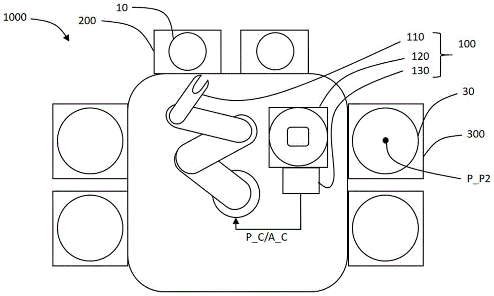
参照图2及图3,本揭示提供一种基板传送设备100,适于将所述基板10从一下货区200传送至一载台30上。所述基板传送设备100包括一传送装置110以及一定位装置120。所述传送装置110用以承托所述基板10并传送所述基板10到所述载台30上。所述定位装置120设置于所述下货区200与所述载台30之间,用以定位所述基板10的一待测位置M_P。所述传送装置110用以于传送所述基板10至所述载台30上之前,先传送所述基板10至所述定位装置120进行定位。所述定位装置120用以计算所述基板10的所述待测位置M_P。若所述待测位置M_P与一第一默认位置P_P1相同,则所述定位装置120提供一默认传送坐标P_C至所述传送装置110,以使所述基板10能被所述传送装置110传送至所述载台30上之一第二默认位置P_P2。若所述待测位置M_P与所述第一默认位置P_P1不同,则所述定位装置120提供一修正传送坐标A_C至所述传送装置110,以使所述基板10能被所述传送装置110传送至所述载台30上之所述第二默认位置P_P2。所述修正传送坐标A_C包含所述预设传送坐标P_C以及一坐标修正值。所述第一默认位置P_P1为一默认圆心坐标P_CC,所述待测位置M_P为所述基板10的一圆心坐标检测值M_CC,且所述坐标修正值为所述圆心坐标检测值M_CC与所述预设圆心坐标P_CC的差值。Referring to FIG. 2 and FIG. 3 , the present disclosure provides a
具体的,所述基板传送设备100应先进行校正,使得若所述待测位置M_P与所述第一默认位置P_P1相同时,所述传送装置110能以所述默认传送坐标P_C将所述基板10送至所述载台30的所述第二默认位置P_P2。图3所示为所述待测位置M_P与所述第一默认位置P_P1不相同的例子。图2、图3中,第一默认位置P_P1或第二默认位置P_P2的黑点仅为说明示意之用,并非表示在所述基板传送设备100中必须画出对位的黑点或记号。Specifically, the
具体的,图3所示为透明的基板10,故可透过基板看到下方的传送装置110。传送装置110例如为机械手臂,本发明不限于此。图6所示为不透明或透明度较低的基板10’。Specifically, FIG. 3 shows a
具体的,因为基板10多半为圆形,具有对称性,所以采用圆心坐标来做为定位的基准,可以快速准确的达成基板的定位。而且对于有翘曲的基板或是对位缺口的基板亦可适用。Specifically, since the
参照图4,于本揭示其中之一实施例中,所述定位装置120包括一取像单元121以及一背光单元122相对所述取像单元121而设置。所述背光单元122的一光轴O_A与所述取像单元121的一光轴O_A’重迭。所述传送装置110用以将所述基板10传送至所述背光单元122与所述取像单元121之间,以使所述基板10位于所述取像单元121的一取像范围C_F中。Referring to FIG. 4 , in one embodiment of the present disclosure, the
具体的,背光单元122的一光轴O_A与所述取像单元121的一光轴O_A’重迭,且光轴O_A垂直传送装置110的承托平面,可以使取像单元121获取的影像不致产生畸变,降低辨识与运算的难度,缩短制程时间。Specifically, an optical axis O_A of the
于本揭示其中之一实施例中,所述第一默认位置P_P1位于所述背光单元122与所述取像单元121之间的所述取像范围C_F之中。In one embodiment of the present disclosure, the first default position P_P1 is located in the image capturing range C_F between the
参照图5,于本揭示其中之一实施例中,当所述传送装置110抵达一默认装置位置P_DP时,所述定位装置120才检测所述基板10是否位于所述第一默认位置P_P1,且所述默认装置位置P_DP位于所述背光单元122与所述取像单元121之间。5, in one embodiment of the present disclosure, when the
具体的,传送装置110应先校正,使得传送装置110能准确抵达所述默认装置位置P_DP。当所述传送装置110抵达一默认装置位置P_DP时,触发所述定位装置120检测所述基板10的位置。Specifically, the
于本揭示其中之一实施例中,所述待测位置M_P为所述基板10的多个所述圆心坐标检测值M_CC的平均值。In one embodiment of the present disclosure, the to-be-measured position M_P is an average value of a plurality of the center coordinate detection values M_CC of the
具体的,虽然仅提供一小段圆弧也可计算出圆心位置,但是对于有翘曲状况的基板,只以一小段圆弧来计算圆心会有较大的误差,因此本揭示取较大范围的圆影像,计算出多个圆心坐标并加以平均,以取得较佳的对位结果。Specifically, although only a small segment of the arc can be used to calculate the position of the center of the circle, for a substrate with warped conditions, there will be a large error in calculating the center of the circle with only a small segment of the arc. Therefore, the present disclosure takes a larger range of Circle image, calculate and average the coordinates of multiple circle centers to obtain better alignment results.
参照图2,于本揭示其中之一实施例中,所述定位装置120包含一运算单元130,用以计算所述基板10的所述圆心坐标检测值M_CC。所述圆心坐标检测值是由所述运算装置以一图形比对法(Pattern Match)、一圆弧计算法(Curve Fit)或一圆适配卡尺法(CircleFit Caliper)其中之一计算而得到。Referring to FIG. 2 , in one embodiment of the present disclosure, the
具体的,图形比对法需要完整的基板影像,且适用于不透明或透明度较低的基板。图形比对法将基板影像切成小块面积,并计算所有小块面积所形成的图案重心位置,即为基板的圆心位置。圆弧计算法适用于透明或不透明的基板。圆弧计算法将基板的圆周适当分割成数小段,计算每一段圆弧的中垂线。圆弧小段之间可以部分重迭。两条中垂线的交会处便是圆心位置。本揭示计算多个圆心位置后加以平均,并设定上下限以便在计算平均圆心位置前消去坐标值过度偏离的圆心。圆适配卡尺法适用于透明、不透明或翘曲的基板。圆适配卡尺法是以软件卡尺在基板影像圆周上进行适配,建构最佳拟合圆(VirtualCircle))而获得圆心坐标。本揭示以软件卡尺适配多段圆弧段取得多个圆心坐标后再取平均值以降低误差。Specifically, the pattern comparison method requires a complete image of the substrate and is suitable for opaque or less transparent substrates. The pattern comparison method cuts the substrate image into small areas, and calculates the position of the center of gravity of the pattern formed by all the small areas, which is the center of the substrate. The arc calculation method is suitable for transparent or opaque substrates. In the arc calculation method, the circumference of the substrate is appropriately divided into several small sections, and the mid-perpendicular line of each arc is calculated. Arc segments can partially overlap. The intersection of the two perpendicular lines is the center of the circle. The present disclosure calculates a plurality of circle center positions and then averages them, and sets upper and lower limits to eliminate the circle centers whose coordinate values are excessively deviated before calculating the average circle center position. The circular-fit caliper method is suitable for transparent, opaque, or warped substrates. The circle fitting caliper method uses software calipers to fit on the circumference of the substrate image to construct the best fitting circle (VirtualCircle) to obtain the coordinates of the center of the circle. In the present disclosure, a software caliper is adapted to a plurality of arc segments to obtain the coordinates of a plurality of circle centers, and then average values are obtained to reduce errors.
于本揭示其中之一实施例中,所述定位装置用以操作所述取像单元获取所述基板的完整影像。In one embodiment of the present disclosure, the positioning device is used to operate the imaging unit to acquire a complete image of the substrate.
参照图2及图3,本揭示还提供一种半导体制程机台1000包括一反应腔300、一下货区200以及一基板传送设备100。所述反应腔300用以进行半导体制程。所述反应腔300中设置一载台30。所述下货区200用以放置至少一基板10。所述基板传送设备100包括一传送装置110以及一定位装置120。所述传送装置110用以承托所述基板10并将所述基板10从所述下货区200传送到所述载台30上。所述定位装置120设置于所述下货区200与所述载台30之间,用以定位所述基板10的一待测位置M_P。所述传送装置110用以于传送所述基板10至所述载台30上之前,先传送所述基板10至所述定位装置120进行定位。所述定位装置120用以计算所述基板10的所述待测位置M_P。若所述待测位置M_P与一第一默认位置P_P1相同,则所述定位装置120提供一默认传送坐标P_C至所述传送装置110,以使所述基板10能被所述传送装置110传送至所述载台30上之一第二默认位置P_P2。若所述待测位置M_P与所述第一默认位置P_P1不同,则所述定位装置120提供一修正传送坐标A_C至所述传送装置110,以使所述基板10能被所述传送装置110传送至所述载台30上之所述第二默认位置P_P2。其中所述修正传送坐标A_C包含所述预设传送坐标P_C以及一坐标修正值。所述第一默认位置P_P1为一默认圆心坐标P_CC,所述待测位置M_P为所述基板10的一圆心坐标检测值M_CC,且所述坐标修正值为所述圆心坐标检测值M_CC与所述预设圆心坐标P_CC的差值。Referring to FIG. 2 and FIG. 3 , the present disclosure further provides a
具体的,所述基板传送设备100应先进行校正,使得若所述待测位置M_P与所述第一默认位置P_P1相同时,所述传送装置110能以所述默认传送坐标P_C将所述基板10送至所述载台30的所述第二默认位置P_P2。图3所示为所述待测位置M_P与所述第一默认位置P_P1不相同的例子。图2、图3中,第一默认位置P_P1或第二默认位置P_P2的黑点仅为说明示意之用,并非表示在所述基板传送设备100中必须画出对位的黑点或记号。Specifically, the
具体的,图3所示为透明的基板10,故可透过基板看到下方的传送装置110。传送装置110例如为机械手臂,本发明不限于此。图6所示为不透明或透明度较低的基板10’。Specifically, FIG. 3 shows a
具体的,因为基板10多半为圆形,具有对称性,所以采用圆心坐标来做为定位的基准,可以快速准确的达成基板的定位。而且对于有翘曲的基板或是对位缺口的基板亦可适用。Specifically, since the
具体的,图2所示半导体制程机台1000的下货区200、反应腔300等的数目与配置仅为说明之用,本揭示不限于此。Specifically, the numbers and configurations of the
具体的,载台30例如为转盘(Spin Chuck)。基板10例如为晶圆(Wafer)。下货区200可设置晶圆卡匣(Wafer Cassette)以承载多个晶圆。Specifically, the
参照图4,于本揭示其中之一实施例的半导体制程机台1000中,所述定位装置120包括一取像单元121以及一背光单元122相对所述取像单元121而设置。所述背光单元122的一光轴O_A与所述取像单元121的一光轴O_A’重迭。所述传送装置110用以将所述基板10传送至所述背光单元122与所述取像单元121之间,以使所述基板10位于所述取像单元121的一取像范围C_F中。Referring to FIG. 4 , in the
具体的,背光单元122的一光轴O_A与所述取像单元121的一光轴O_A’重迭,且光轴O_A垂直传送装置110的承托平面,可以使取像单元121获取的影像不致产生畸变,降低辨识与运算的难度,缩短制程时间。具体的,取像单元121的一光轴O_A’大致与基板10的对称轴重迭以获取畸变程度较低的影像。Specifically, an optical axis O_A of the
参照图7,本揭示还提供一种基板传送方法,适于将所述基板10从一下货区200传送至一载台30上,其中所述基板传送方法包括:步骤S10:提供一传送装置110;步骤S20:提供一定位装置120,设置于所述下货区200与所述载台30之间;步骤S30:所述传送装置110承托所述基板10并将所述基板10传送至所述定位装置120;步骤S40:所述定位装置120检测所述基板10的一待测位置M_P;步骤S50:所述定位装置120判断所述待测位置M_P与一第一默认位置P_P1是否相同,若所述待测位置M_P与一第一默认位置P_P1相同则执行步骤S60:所述定位装置120提供一默认传送坐标P_C至所述传送装置110;步骤S70:所述传送装置110依所述默认传送坐标P_C传送所述基板10至所述载台30上之一第二默认位置P_P2;若所述待测位置M_P与所述第一默认位置P_P1不同,则执行步骤S80:所述定位装置120提供一修正传送坐标A_C至所述传送装置110;以及步骤S90:所述传送装置110依所述修正传送坐标A_C传送所述基板10至所述载台30上之所述第二默认位置P_P2。其中所述修正传送坐标A_C包含所述预设传送坐标P_C以及一坐标修正值,所述第一默认位置P_P1为一默认圆心坐标P_CC,所述待测位置M_P为所述基板10的一圆心坐标检测值M_CC,且所述坐标修正值为所述圆心坐标检测值M_CC与所述预设圆心坐标P_CC的差值。Referring to FIG. 7 , the present disclosure further provides a substrate transfer method suitable for transferring the substrate 10 from the lower cargo area 200 to a carrier 30 , wherein the substrate transfer method includes: step S10 : providing a transfer device 110 ; Step S20: provide a positioning device 120, disposed between the loading area 200 and the carrier 30; Step S30: the transfer device 110 supports the substrate 10 and transfers the substrate 10 to the Step S40: the positioning device 120 detects a position to be measured M_P of the substrate 10; Step S50: the positioning device 120 determines whether the position to be measured M_P is the same as a first default position P_P1, If the to-be-measured position M_P is the same as a first default position P_P1 , step S60 is executed: the positioning device 120 provides a default transmission coordinate P_C to the transmission device 110 ; Step S70 : the transmission device 110 follows the default Transfer the coordinates P_C to transfer the substrate 10 to a second default position P_P2 on the stage 30 ; if the position to be measured M_P is different from the first default position P_P1 , step S80 is executed: the positioning device 120 Provide a modified transfer coordinate A_C to the transfer device 110 ; and step S90 : the transfer device 110 transfers the substrate 10 to the second default position P_P2 on the stage 30 according to the modified transfer coordinate A_C. The corrected transfer coordinate A_C includes the preset transfer coordinate P_C and a coordinate correction value, the first default position P_P1 is a default center coordinate P_CC, and the to-be-measured position M_P is a center coordinate of the
相较于先前技术,本揭示的基板传送设备、半导体制程机台以及基板传送方法藉由定位装置的取像单元以及背光单元检测并取得基板的圆心坐标检测值,修正传送装置的传送坐标,如此可快速准确的提供晶圆定位,不受晶圆翘曲的影响,有效地避免现有技术中的问题。Compared with the prior art, the substrate transfer apparatus, the semiconductor process machine, and the substrate transfer method of the present disclosure detect and obtain the detection value of the coordinates of the center of the substrate by the imaging unit and the backlight unit of the positioning device, and correct the transfer coordinates of the transfer device, so that The wafer positioning can be provided quickly and accurately, and is not affected by the warpage of the wafer, thus effectively avoiding the problems in the prior art.
尽管已经相对于一个或多个实现方式示出并描述了本揭示,但是本领域技术人员基于对本说明书和附图的阅读和理解将会想到等价变型和修改。本揭示包括所有这样的修改和变型,并且仅由所附权利要求的范围限制。特别地关于由上述组件执行的各种功能,用于描述这样的组件的术语旨在对应于执行所述组件的指定功能(例如其在功能上是等价的)的任意组件(除非另外指示),即使在结构上与执行本文所示的本说明书的示范性实现方式中的功能的公开结构不等同。此外,尽管本说明书的特定特征已经相对于若干实现方式中的仅一个被公开,但是这种特征可以与如可以对给定或特定应用而言是期望和有利的其他实现方式的一个或多个其他特征组合。而且,就术语“包括”、“具有”、“含有”或其变形被用在具体实施方式或权利要求中而言,这样的术语旨在以与术语“包含”相似的方式包括。While the disclosure has been shown and described with respect to one or more implementations, equivalent variations and modifications will occur to those skilled in the art based on a reading and understanding of this specification and the accompanying drawings. The present disclosure includes all such modifications and variations and is limited only by the scope of the appended claims. In particular with respect to the various functions performed by the above-described components, the terms used to describe such components are intended to correspond to any component that performs the specified function of the component (eg, which is functionally equivalent) (eg, which is functionally equivalent) (unless otherwise indicated) , even if it is not structurally equivalent to the disclosed structure that performs the functions of the exemplary implementations of the specification shown herein. Furthermore, although a particular feature of this specification has been disclosed with respect to only one of several implementations, such feature may be combined with one or more of the other implementations as may be desired and advantageous for a given or particular application Other feature combinations. Also, to the extent that the terms "including," "having," "containing," or variations thereof, are used in the detailed description or the claims, such terms are intended to include in a manner similar to the term "comprising."
以上仅是本揭示的优选实施方式,应当指出,对于本领域普通技术人员,在不脱离本揭示原理的前提下,还可以做出若干改进和润饰,这些改进和润饰也应视为本揭示的保护范围。The above are only the preferred embodiments of the present disclosure. It should be pointed out that for those skilled in the art, on the premise of not departing from the principles of the present disclosure, several improvements and modifications can also be made, and these improvements and modifications should also be regarded as the present disclosure. protected range.
Claims (10)
Priority Applications (1)
| Application Number | Priority Date | Filing Date | Title |
|---|---|---|---|
| CN201910561490.5A CN112151429A (en) | 2019-06-26 | 2019-06-26 | Substrate transfer equipment, semiconductor process machine, and substrate transfer method |
Applications Claiming Priority (1)
| Application Number | Priority Date | Filing Date | Title |
|---|---|---|---|
| CN201910561490.5A CN112151429A (en) | 2019-06-26 | 2019-06-26 | Substrate transfer equipment, semiconductor process machine, and substrate transfer method |
Publications (1)
| Publication Number | Publication Date |
|---|---|
| CN112151429A true CN112151429A (en) | 2020-12-29 |
Family
ID=73869784
Family Applications (1)
| Application Number | Title | Priority Date | Filing Date |
|---|---|---|---|
| CN201910561490.5A Pending CN112151429A (en) | 2019-06-26 | 2019-06-26 | Substrate transfer equipment, semiconductor process machine, and substrate transfer method |
Country Status (1)
| Country | Link |
|---|---|
| CN (1) | CN112151429A (en) |
Citations (9)
| Publication number | Priority date | Publication date | Assignee | Title |
|---|---|---|---|---|
| JPS6457104A (en) * | 1987-08-28 | 1989-03-03 | Nikon Corp | Measuring apparatus of amount of positional deviation of circular substrate |
| JPH0936201A (en) * | 1995-05-18 | 1997-02-07 | Toshiba Electron Eng Corp | Substrate transfer method and substrate transfer apparatus |
| JP2003188228A (en) * | 2001-12-18 | 2003-07-04 | Nikon Corp | Substrate transfer method |
| CN1574210A (en) * | 2003-06-16 | 2005-02-02 | 东京毅力科创株式会社 | Substrate processing apparatus and method of aligning substrate carrier apparatus |
| US20160189390A1 (en) * | 2014-12-24 | 2016-06-30 | Tokyo Electron Limited | Substrate transport apparatus and substrate transport method |
| KR20180070386A (en) * | 2016-12-16 | 2018-06-26 | 주식회사 원익아이피에스 | Substrate mounting position correcting method for substrate processing system, and substrate processing method |
| CN108226179A (en) * | 2018-01-10 | 2018-06-29 | 京东方科技集团股份有限公司 | The calibration method of automated optical detection equipment and automatic repair system |
| CN209993581U (en) * | 2019-06-26 | 2020-01-24 | 弘塑科技股份有限公司 | Substrate transfer equipment and semiconductor process equipment |
| US20230117258A1 (en) * | 2021-10-19 | 2023-04-20 | Tokyo Electron Limited | Substrate transfer apparatus and substrate transfer method |
-
2019
- 2019-06-26 CN CN201910561490.5A patent/CN112151429A/en active Pending
Patent Citations (9)
| Publication number | Priority date | Publication date | Assignee | Title |
|---|---|---|---|---|
| JPS6457104A (en) * | 1987-08-28 | 1989-03-03 | Nikon Corp | Measuring apparatus of amount of positional deviation of circular substrate |
| JPH0936201A (en) * | 1995-05-18 | 1997-02-07 | Toshiba Electron Eng Corp | Substrate transfer method and substrate transfer apparatus |
| JP2003188228A (en) * | 2001-12-18 | 2003-07-04 | Nikon Corp | Substrate transfer method |
| CN1574210A (en) * | 2003-06-16 | 2005-02-02 | 东京毅力科创株式会社 | Substrate processing apparatus and method of aligning substrate carrier apparatus |
| US20160189390A1 (en) * | 2014-12-24 | 2016-06-30 | Tokyo Electron Limited | Substrate transport apparatus and substrate transport method |
| KR20180070386A (en) * | 2016-12-16 | 2018-06-26 | 주식회사 원익아이피에스 | Substrate mounting position correcting method for substrate processing system, and substrate processing method |
| CN108226179A (en) * | 2018-01-10 | 2018-06-29 | 京东方科技集团股份有限公司 | The calibration method of automated optical detection equipment and automatic repair system |
| CN209993581U (en) * | 2019-06-26 | 2020-01-24 | 弘塑科技股份有限公司 | Substrate transfer equipment and semiconductor process equipment |
| US20230117258A1 (en) * | 2021-10-19 | 2023-04-20 | Tokyo Electron Limited | Substrate transfer apparatus and substrate transfer method |
Similar Documents
| Publication | Publication Date | Title |
|---|---|---|
| CN103247559B (en) | Substrate transfer apparatus and substrate transfer method | |
| CN109994404B (en) | Teaching method | |
| JP5516482B2 (en) | Substrate transport method, substrate transport apparatus, and coating and developing apparatus | |
| CN103247558B (en) | Substrate board treatment and substrate processing method using same | |
| JP5324232B2 (en) | Semiconductor wafer alignment system | |
| JP5309157B2 (en) | System and method for calibrating end effector alignment in a plasma processing system | |
| US20140124479A1 (en) | Method of removing coating film of substrate peripheral portion, substrate processing apparatus and non-transitory storage medium | |
| US20210252695A1 (en) | Teaching method | |
| JP2010161192A (en) | Alignment apparatus for semiconductor wafer | |
| CN104723362A (en) | Robotic system and detection method | |
| US7406360B2 (en) | Method for detecting transfer shift of transfer mechanism and semiconductor processing equipment | |
| TW201727704A (en) | Liquid processing device, liquid processing method and memory medium | |
| JPH09306977A (en) | Wafer positioning method in wafer inspection apparatus etc. | |
| KR20190008102A (en) | Substrate position adjustment method, storage medium and substrate processing system | |
| CN105278266A (en) | Deviation detection and correction method for glass substrate | |
| CN209993581U (en) | Substrate transfer equipment and semiconductor process equipment | |
| JP2005101455A (en) | Positioning device | |
| TWI397943B (en) | Position correction device, vacuum processing device, and position correction method | |
| CN112151429A (en) | Substrate transfer equipment, semiconductor process machine, and substrate transfer method | |
| TWI711115B (en) | Substrate transferring apparatus, semiconductor process machine and substrate transferring method | |
| TWM585428U (en) | Substrate transferring apparatus and semiconductor process machine | |
| CN1838398A (en) | Substrate processing apparatus and substrate housing method | |
| KR101478898B1 (en) | Charged particle beam writing apparatus and charged particle beam writing method | |
| US10510569B2 (en) | Pattern forming apparatus and manufacturing method for semiconductor device | |
| JPS6220343A (en) | Wafer positioning device |
Legal Events
| Date | Code | Title | Description |
|---|---|---|---|
| PB01 | Publication | ||
| PB01 | Publication | ||
| SE01 | Entry into force of request for substantive examination | ||
| SE01 | Entry into force of request for substantive examination | ||
| RJ01 | Rejection of invention patent application after publication |
Application publication date: 20201229 |
|
| RJ01 | Rejection of invention patent application after publication |