CN112018052A - Semiconductor package with laser activatable molding compound - Google Patents
Semiconductor package with laser activatable molding compound Download PDFInfo
- Publication number
- CN112018052A CN112018052A CN202010448139.8A CN202010448139A CN112018052A CN 112018052 A CN112018052 A CN 112018052A CN 202010448139 A CN202010448139 A CN 202010448139A CN 112018052 A CN112018052 A CN 112018052A
- Authority
- CN
- China
- Prior art keywords
- laser
- molding compound
- metal
- layer
- activatable
- Prior art date
- Legal status (The legal status is an assumption and is not a legal conclusion. Google has not performed a legal analysis and makes no representation as to the accuracy of the status listed.)
- Pending
Links
Images


Classifications
-
- H10P72/74—
-
- H10W74/114—
-
- H10W72/90—
-
- H10W72/012—
-
- H10W72/015—
-
- H10W72/20—
-
- H10W72/50—
-
- H10W74/014—
-
- H10W74/016—
-
- H10W74/019—
-
- H10W74/129—
-
- H10W90/701—
-
- H10P72/7416—
-
- H10P72/7436—
-
- H10P72/7438—
-
- H10W70/05—
-
- H10W70/09—
-
- H10W70/099—
-
- H10W70/60—
-
- H10W70/65—
-
- H10W70/652—
-
- H10W70/654—
-
- H10W70/66—
-
- H10W72/019—
-
- H10W72/01923—
-
- H10W72/01925—
-
- H10W72/01935—
-
- H10W72/01955—
-
- H10W72/01961—
-
- H10W72/0198—
-
- H10W72/073—
-
- H10W72/29—
-
- H10W72/874—
-
- H10W72/922—
-
- H10W72/923—
-
- H10W72/9413—
-
- H10W72/944—
-
- H10W72/952—
-
- H10W74/142—
-
- H10W90/736—
Landscapes
- Engineering & Computer Science (AREA)
- Microelectronics & Electronic Packaging (AREA)
- Computer Hardware Design (AREA)
- Power Engineering (AREA)
- Manufacturing & Machinery (AREA)
- Physics & Mathematics (AREA)
- Condensed Matter Physics & Semiconductors (AREA)
- General Physics & Mathematics (AREA)
- Encapsulation Of And Coatings For Semiconductor Or Solid State Devices (AREA)
- Structures Or Materials For Encapsulating Or Coating Semiconductor Devices Or Solid State Devices (AREA)
Abstract
本发明提供了模制封装和对应制造方法的实施例。在模制封装的实施例中,所述模制封装包括具有多个激光活化区的可激光活化模制化合物,所述多个激光活化区镀覆有导电材料,以在可激光活化模制化合物的第一侧处形成金属焊盘和/或金属迹线。嵌入可激光活化模制化合物中的半导体管芯具有多个管芯焊盘。互连将半导体管芯的多个管芯焊盘电连接到可激光活化模制化合物的第一侧处的金属焊盘和/或金属迹线。
The present invention provides embodiments of a molded package and corresponding method of manufacture. In an embodiment of a molded package, the molded package includes a laser-activatable molding compound having a plurality of laser-activated regions plated with a conductive material to allow the laser-activatable molding compound to Metal pads and/or metal traces are formed at the first side of the . The semiconductor die embedded in the laser-activatable molding compound has a plurality of die pads. The interconnect electrically connects the plurality of die pads of the semiconductor die to metal pads and/or metal traces at the first side of the laser-activatable molding compound.
Description
技术领域technical field
本公开总体上涉及半导体管芯封装的领域,并且更具体地涉及形成包 括封装互连的模制封装的领域。The present disclosure relates generally to the field of semiconductor die packaging, and more particularly to the field of forming molded packages including package interconnects.
背景技术Background technique
半导体器件制造商一直在努力提高其产品性能,同时降低他们的制造 成本。半导体器件制造中的成本和器件性能敏感区域是封装半导体管芯。封 装涉及包封半导体管芯和形成从管芯焊盘到封装端子的互连。封装概念和 互连技术应当提供半导体器件的高的电性能和热性能以及可靠性。它们应 当进一步支持封装可缩放性和管芯收缩。Semiconductor device manufacturers are constantly striving to improve the performance of their products while reducing their manufacturing costs. A cost and device performance sensitive area in semiconductor device fabrication is the packaging of the semiconductor die. Packaging involves encapsulating a semiconductor die and forming interconnects from die pads to package terminals. Packaging concepts and interconnection techniques should provide high electrical and thermal performance and reliability of semiconductor devices. They should further support package scalability and die shrink.
此外,很多类型的半导体器件对诸如寄生互连电阻和电感、寄生电容耦 合等的寄生电效应高度敏感。例如,开关、功率晶体管、RF(射频)功率放 大器、低噪声放大器(LNA)、天线调谐器、混频器等均对寄生电效应高度 敏感。用于减少封装半导体器件上的寄生电效应的技术常常会导致更高的 总成本、更大的封装大小、更复杂的制造工艺、降低的器件性能等。Furthermore, many types of semiconductor devices are highly sensitive to parasitic electrical effects such as parasitic interconnect resistance and inductance, parasitic capacitive coupling, and the like. For example, switches, power transistors, RF (radio frequency) power amplifiers, low noise amplifiers (LNA), antenna tuners, mixers, etc. are all highly sensitive to parasitic electrical effects. Techniques for reducing parasitic electrical effects on packaged semiconductor devices often result in higher overall costs, larger package sizes, more complex manufacturing processes, reduced device performance, and the like.
发明内容SUMMARY OF THE INVENTION
根据模制封装的实施例,所述模制封装包括:可激光活化模制化合物, 所述可激光活化模制化合物具有多个激光活化区,所述多个激光活化区镀 覆有导电材料,以在可激光活化模制化合物的第一侧处形成金属焊盘和/或 金属迹线;半导体管芯,所述半导体管芯嵌入在可激光活化模制化合物中, 并且具有多个管芯焊盘;以及互连,所述互连将半导体管芯的多个管芯焊盘 电连接到可激光活化模制化合物的第一侧处的金属焊盘和/或金属迹线。According to an embodiment of a molding package, the molding package includes a laser-activatable molding compound, the laser-activatable molding compound having a plurality of laser-activated regions plated with a conductive material, to form metal pads and/or metal traces at a first side of the laser activatable molding compound; a semiconductor die embedded in the laser activatable molding compound and having a plurality of die bond a pad; and an interconnect that electrically connects the plurality of die pads of the semiconductor die to metal pads and/or metal traces at the first side of the laser-activatable molding compound.
可激光活化模制化合物可以是单层模制化合物或多层模制化合物。The laser-activatable molding compound may be a single-layer molding compound or a multi-layer molding compound.
如果可激光活化模制化合物是单层模制化合物,在一个实施例中,互连 包括多个线螺柱凸块或金属柱或垂直键合线,所述线螺柱凸块或金属柱或 垂直键合线在第一端部处附接到半导体管芯的多个管芯焊盘,并且在与第 一端部相对的第二端部处附接到可激光活化模制化合物的第一侧处的金属 焊盘和/或金属迹线。If the laser-activatable molding compound is a single-layer molding compound, in one embodiment, the interconnect includes a plurality of wire stud bumps or metal posts or vertical bond wires, the wire stud bumps or metal posts or A vertical bond wire is attached to the plurality of die pads of the semiconductor die at a first end and to a first of the laser-activatable molding compound at a second end opposite the first end Metal pads and/or metal traces at the sides.
如果可激光活化模制化合物是多层模制化合物,在一个实施例中,互连 包括多个线螺柱凸块或金属柱或垂直键合线,所述线螺柱凸块或金属柱或 垂直键合线在第一端部处附接到半导体管芯的多个管芯焊盘,并且在与第 一端部相对的第二端部处附接到可激光活化模制化合物的第一层的第一层 金属结构,其中,可激光活化模制化合物的第一层具有多个激光活化区,所 述多个激光活化区镀覆有导电材料,以形成第一层金属结构。If the laser-activatable molding compound is a multi-layer molding compound, in one embodiment, the interconnect includes a plurality of wire stud bumps or metal posts or vertical bond wires, the wire stud bumps or metal posts or A vertical bond wire is attached to the plurality of die pads of the semiconductor die at a first end and to a first of the laser-activatable molding compound at a second end opposite the first end A first-layer metal structure of layers, wherein the first layer of laser-activatable molding compound has a plurality of laser-activated regions plated with conductive material to form the first-layer metal structure.
如果可激光活化模制化合物是多层模制化合物,模制封装还包括可激 光活化模制化合物的第二层,其中,可激光活化模制化合物的第二层可以具 有多个激光活化区,所述多个激光活化区镀覆有导电材料,以形成可激光活 化模制化合物的第二层的第二层金属结构,其中,可激光活化模制化合物的 第一层的第一层金属结构电连接到可激光活化模制化合物的第二层的第二 层金属结构。If the laser-activatable molding compound is a multilayer molding compound, the molding package further includes a second layer of the laser-activatable molding compound, wherein the second layer of the laser-activatable molding compound may have a plurality of laser-activated regions, The plurality of laser-activated regions are coated with a conductive material to form a second-layer metal structure of the second layer of laser-activatable molding compound, wherein the first-layer metal structure of the first layer of laser-activatable molding compound The second layer metal structure is electrically connected to the second layer of the laser activatable molding compound.
单独地或组合地,所述模制封装还可以包括覆盖可激光活化模制化合 物的第一侧的部分的阻焊剂层,使得在第一侧,仅暴露金属焊盘和/或金属 迹线的部分,以形成模制封装的着陆焊盘。Alone or in combination, the mold package may also include a solder resist layer covering a portion of the first side of the laser-activatable mold compound, such that on the first side, only the metal pads and/or metal traces are exposed. part to form the landing pads of the molded package.
单独地或组合地,多个管芯焊盘可以设置在半导体管芯的第一侧处,半 导体管芯的与第一侧相对的第二侧可以不被可激光活化模制化合物覆盖, 并且模制封装还可以包括覆盖半导体管芯的第二侧的顶部密封或覆盖半导 体管芯的第二侧的热沉金属板。Individually or in combination, the plurality of die pads may be disposed at a first side of the semiconductor die, a second side of the semiconductor die opposite the first side may not be covered by the laser-activatable molding compound, and the mold may be The manufacturing package may also include a top seal covering the second side of the semiconductor die or a heat sink metal plate covering the second side of the semiconductor die.
单独地或组合地,多个管芯焊盘可以设置在半导体管芯的第一侧处,半 导体管芯的与第一侧相对的第二侧可以不被可激光活化模制化合物覆盖, 可激光活化模制化合物可以比半导体管芯更厚,并且可激光活化模制化合 物在半导体管芯的第二侧处可以具有凹陷区。Individually or in combination, the plurality of die pads may be disposed at a first side of the semiconductor die, and a second side of the semiconductor die opposite the first side may not be covered by the laser-activatable molding compound, which may be laser activatable. The activatable molding compound may be thicker than the semiconductor die, and the laser activatable molding compound may have a recessed region at the second side of the semiconductor die.
可激光活化模制化合物的凹陷区可以形成模制封装内的开放腔体。The recessed regions of the laser-activatable molding compound can form open cavities within the molded package.
单独地或组合地,模制封装还可以包括设置在可激光活化模制化合物 的凹陷区中的热沉。Alone or in combination, the mold package may also include a heat sink disposed in the recessed region of the laser-activatable mold compound.
单独地或组合地,可激光活化模制化合物的第一侧处的金属焊盘和/或 金属迹线可以是约1μm到约80μm厚,例如约5μm到约20μm厚。Alone or in combination, the metal pads and/or metal traces at the first side of the laser-activatable molding compound may be about 1 μm to about 80 μm thick, such as about 5 μm to about 20 μm thick.
单独地或组合地,半导体管芯可以包括功率晶体管、RF前端电路、逻 辑器件,或者可以是控制器。Alone or in combination, the semiconductor die may include power transistors, RF front-end circuits, logic devices, or may be a controller.
单独地或组合地,可激光活化模制化合物的第一侧处的金属焊盘的第 一个可以通过互连来电连接到半导体管芯的管芯焊盘的第一个,并且在第 一管芯焊盘的覆盖区到可激光活化模制化合物的第一侧的垂直投影中,第 一金属焊盘可以定位于第一管芯焊盘的覆盖区外部。Alone or in combination, a first one of the metal pads at the first side of the laser activatable molding compound can be electrically connected to the first one of the die pads of the semiconductor die by an interconnect, and the first one of the metal pads at the first side of the In a vertical projection of the footprint of the die pad onto the first side of the laser-activatable molding compound, the first metal pad may be positioned outside the footprint of the first die pad.
第一金属焊盘可以连接到可激光活化模制化合物的第一侧处的金属迹 线的第一个,并且在垂直投影中,第一金属迹线可以定位于第一管芯焊盘的 覆盖区内部,并且与第一管芯焊盘垂直对准。The first metal pad may be connected to a first one of the metal traces at the first side of the laser-activatable molding compound, and in vertical projection, the first metal trace may be positioned overlying the first die pad inside the region and vertically aligned with the first die pad.
根据制造模制封装的方法的实施例,所述方法包括:在载体上放置半导 体管芯,所述半导体管芯具有背离载体的多个管芯焊盘;在载体上放置半导 体管芯之前或之后,将互连的至少初始部分附接到半导体管芯的多个管芯 焊盘;将半导体管芯和互连嵌入可激光活化模制化合物中;将激光引导到可 激光活化模制化合物的第一侧,以激光活化可激光活化模制化合物的多个 区;以及在可激光活化模制化合物的多个激光活化区上镀覆导电材料,以在 可激光活化模制化合物的第一侧处形成金属焊盘和/或金属迹线,其中,互 连将半导体管芯的多个管芯焊盘电连接到可激光活化模制化合物的第一侧 处的金属焊盘和/或金属迹线。According to an embodiment of a method of manufacturing a molded package, the method includes: placing a semiconductor die on a carrier, the semiconductor die having a plurality of die pads facing away from the carrier; before or after placing the semiconductor die on the carrier , attaching at least an initial portion of the interconnect to a plurality of die pads of the semiconductor die; embedding the semiconductor die and interconnect in the laser-activatable molding compound; directing the laser to the first portion of the laser-activatable molding compound one side, laser-activating the plurality of regions of the laser-activatable molding compound; and plating a conductive material on the plurality of laser-activatable regions of the laser-activatable molding compound to be at the first side of the laser-activatable molding compound forming metal pads and/or metal traces, wherein the interconnect electrically connects the plurality of die pads of the semiconductor die to the metal pads and/or metal traces at the first side of the laser-activatable molding compound .
在一个实施例中,模制化合物可以是多层模制化合物。在这种情况下, 将半导体管芯和互连嵌入可激光活化模制化合物中包括:将半导体管芯和 互连的初始部分嵌入可激光活化模制化合物的第一层中;将激光引导到可 激光活化模制化合物的第一层,以激光活化可激光活化模制化合物的第一 层的多个区;在可激光活化模制化合物的第一层的多个激光活化区上镀覆 导电材料,以在可激光活化模制化合物的第一层的表面处形成第一层金属 结构;以及在可激光活化模制化合物的第一层的表面之上施加可激光活化 模制化合物的第二层。In one embodiment, the molding compound may be a multi-layer molding compound. In this case, embedding the semiconductor die and interconnects in the laser-activatable molding compound includes: embedding an initial portion of the semiconductor die and interconnects in the first layer of the laser-activatable molding compound; directing the laser light into the laser-activatable molding compound; a first layer of laser activatable molding compound to laser activate a plurality of regions of the first layer of laser activatable molding compound; plating conductive on the plurality of laser activated regions of the first layer of laser activatable molding compound material to form a first layer of metal structure at the surface of the first layer of laser activatable molding compound; and applying a second layer of laser activatable molding compound over the surface of the first layer of laser activatable molding compound Floor.
在一个实施例中,将互连的至少初始部分附接到半导体管芯的多个管 芯焊盘包括将多个线螺柱凸块或金属柱或垂直键合线附接到半导体管芯的 多个管芯焊盘。In one embodiment, attaching at least an initial portion of the interconnect to the plurality of die pads of the semiconductor die includes attaching a plurality of wire stud bumps or metal posts or vertical bond wires to the semiconductor die multiple die pads.
单独地或组合地,所述方法还可以包括用阻焊剂层覆盖可激光活化模 制化合物的第一侧的部分,使得在第一侧处,仅暴露金属焊盘和/或金属迹 线的部分,以形成模制封装的着陆焊盘。Alone or in combination, the method may also include covering a portion of the first side of the laser-activatable molding compound with a layer of solder resist such that at the first side, only portions of the metal pads and/or metal traces are exposed , to form the landing pads of the molded package.
单独地或组合地,所述方法还可以包括:在可激光活化模制化合物的多 个激光活化区上镀覆导电材料之后,从半导体管芯移除载体,以暴露半导体 管芯的与管芯焊盘相对的一侧;以及用顶部密封或用热沉金属板覆盖半导 体管芯的通过移除载体而暴露的一侧。Alone or in combination, the method may further include removing the carrier from the semiconductor die after plating the conductive material on the plurality of laser-activated regions of the laser-activatable molding compound to expose the semiconductor die and the die. the side opposite the pad; and the side of the semiconductor die exposed by removing the carrier is covered with a top seal or with a heat sink metal plate.
单独地或组合地,将半导体管芯和互连嵌入可激光活化模制化合物中 可以包括用可激光活化模制化合物(如果可激光活化模制化合物是多层模 制化合物,用可激光活化模制化合物的第一层)来覆盖互连,并且所述方法 还可以包括减薄(例如通过研磨)可激光活化模制化合物(如果可激光活化 模制化合物是多层模制化合物,特别是可激光活化模制化合物的第一层), 以在背离载体的一侧暴露互连的至少初始部分。Alone or in combination, embedding the semiconductor die and interconnects in the laser activatable molding compound may include using the laser activatable molding compound (if the laser activatable molding compound is a multilayer molding compound, with the laser activatable molding compound) forming a first layer of compound) to cover the interconnects, and the method may further comprise thinning (eg, by grinding) the laser-activatable molding compound (if the laser-activatable molding compound is a multilayer molding compound, especially The laser activates a first layer of molding compound) to expose at least an initial portion of the interconnect on the side facing away from the carrier.
单独地或组合地,将半导体管芯和互连嵌入可激光活化模制化合物中 可以包括用可激光活化模制化合物(如果可激光活化模制化合物是多层模 制化合物,用可激光活化模制化合物的第一层)来覆盖互连,并且所述方法 还可以包括在可激光活化模制化合物中(如果可激光活化模制化合物是多 层模制化合物,特别是在可激光活化模制化合物的第一层中)钻孔(例如, 通过激光或机械钻孔),以在背离载体的一侧处暴露互连的至少初始部分。Alone or in combination, embedding the semiconductor die and interconnects in the laser activatable molding compound may include using the laser activatable molding compound (if the laser activatable molding compound is a multilayer molding compound, with the laser activatable molding compound) the first layer of molding compound) to cover the interconnects, and the method may also be included in the laser activatable molding compound (if the laser activatable molding compound is a multilayer molding compound, especially in the laser activatable molding compound A first layer of compound) is drilled (eg, by laser or mechanical drilling) to expose at least an initial portion of the interconnect at the side facing away from the carrier.
单独地或组合地,互连的至少初始部分可以从可激光活化模制化合物 突出,或者,如果可激光活化模制化合物包括第一层和第二层,在背离载体 的一侧处从可激光活化模制化合物的第一层突出。Alone or in combination, at least an initial portion of the interconnect can protrude from the laser activatable molding compound, or, if the laser activatable molding compound includes a first layer and a second layer, from the laser activatable molding compound at the side facing away from the carrier. The first layer of activated molding compound protrudes.
单独地或组合地,所述方法还可以包括在半导体管芯的与多个管芯焊 盘相对的一侧处在可激光活化模制化合物中形成腔体。Alone or in combination, the method may also include forming a cavity in the laser-activatable molding compound at a side of the semiconductor die opposite the plurality of die pads.
本领域的技术人员在阅读以下详细描述并且查看附图时将认识到额外 的特征和优点。Those skilled in the art will recognize additional features and advantages upon reading the following detailed description and reviewing the accompanying drawings.
附图说明Description of drawings
附图的元素未必彼此相对成比例。相似的附图标记指示对应的类似部 分。除非彼此互斥,各种说明性的实施例的特征可以组合。实施例在附图中 被描述,并且在接下来的描述中被详细说明。The elements of the figures are not necessarily to scale with respect to one another. Like reference numerals indicate corresponding similar parts. The features of the various illustrative embodiments may be combined unless mutually exclusive. Embodiments are depicted in the accompanying drawings and detailed in the description that follows.
图1示出了具有用于管芯(芯片)嵌入的可激光活化模制化合物的模 制封装的实施例的截面图。Figure 1 shows a cross-sectional view of an embodiment of a molded package with a laser-activatable molding compound for die (chip) embedding.
图2示出了图1的模制封装的部分平面图。FIG. 2 shows a partial plan view of the molded package of FIG. 1 .
图3A示出了可以用于图1的模制封装中的示例性线螺柱凸块互连的 截面图。3A shows a cross-sectional view of an exemplary wire stud bump interconnect that may be used in the molded package of FIG. 1 .
图3B示出了可以用于图1的模制封装中的示例性柱互连的截面图。3B shows a cross-sectional view of an exemplary pillar interconnect that may be used in the molded package of FIG. 1 .
图3C示出了可以用于图1的模制封装中的示例性垂直键合线互连的 截面图。3C shows a cross-sectional view of an exemplary vertical bond wire interconnect that may be used in the molded package of FIG. 1 .
图4示出了具有用于管芯嵌入的可激光活化模制化合物的模制封装的 另一实施例的截面图。Figure 4 shows a cross-sectional view of another embodiment of a molded package with a laser-activatable molding compound for die embedding.
图5A到图5E示出了根据实施例的在制造具有用于管芯嵌入的可激光 活化模制化合物的模制封装的不同阶段期间的相应的部分截面图。5A-5E illustrate respective partial cross-sectional views during different stages of fabricating a molded package with a laser-activatable molding compound for die embedding, according to an embodiment.
图6A到图6E示出了根据另一实施例的在制造具有用于管芯嵌入的可 激光活化模制化合物的模制封装的不同阶段期间的相应的部分截面图。6A-6E illustrate respective partial cross-sectional views during different stages of manufacturing a molded package with a laser-activatable molding compound for die embedding, according to another embodiment.
图7A到图7D示出了根据又一实施例的在制造具有用于管芯嵌入的可 激光活化模制化合物的模制封装的不同阶段期间的相应的部分截面图。7A-7D illustrate respective partial cross-sectional views during different stages of manufacturing a molded package with a laser-activatable molding compound for die embedding, according to yet another embodiment.
图8示出了通过图5A到图5E、图6A到图6E或图7A到图7D中所 示的任何一种方法生产的模制封装的截面图。Figure 8 shows a cross-sectional view of a molded package produced by any of the methods shown in Figures 5A-5E, Figures 6A-6E, or Figures 7A-7D.
图9A到图9E、图10A到图10E、图11A到图11E以及图12A到图 12E均示出了根据额外的实施例的在制造具有用于管芯嵌入的可激光活化 模制化合物的模制封装的不同阶段期间的相应的部分截面图。FIGS. 9A-9E, 10A-10E, 11A-11E, and 12A-12E each illustrate the fabrication of a mold with a laser-activatable molding compound for die embedding in accordance with additional embodiments. Corresponding partial cross-sectional views during different stages of packaging.
图13示出了在镀覆工艺之后和在载体移除之前通过图9A到图9E、图 10A到图10E、图11A到图11E和图12A到图12E中所示的任何一种方法 生产的结构的部分平面图。FIG. 13 shows the resulting product produced by any of the methods shown in FIGS. 9A-9E, 10A-10E, 11A-11E, and 12A-12E after the plating process and before carrier removal. Partial floor plan of the structure.
图14示出了在镀覆工艺之后和在载体移除之前贯穿通过图9A到图9E、 图10A到图10E、图11A到图11E和图12A到图12E中所示的任何一种方 法生产的一个互连、一个管芯焊盘和一个金属焊盘/金属迹线的截面图。Fig. 14 shows production through any of the methods shown in Figs. 9A-9E, 10A-10E, 11A-11E and 12A-12E after the plating process and prior to carrier removal A cross-sectional view of one interconnect, one die pad, and one metal pad/metal trace.
图15A到图15F示出了在制造具有用于管芯嵌入的单层可激光活化模 制化合物的模制封装的不同阶段期间的示例性透视图和部分截面图。15A-15F show exemplary perspective and partial cross-sectional views during various stages of manufacturing a molded package with a single layer of laser-activatable molding compound for die embedding.
图16示出了具有多个源极区和漏极区的示例性功率晶体管的平面图。16 shows a plan view of an exemplary power transistor having multiple source and drain regions.
图17A到图17J示出了在制造具有用于管芯嵌入的多层可激光活化模 制化合物的模制封装的不同阶段期间的示例性透视图和部分截面图。17A-17J illustrate exemplary perspective and partial cross-sectional views during various stages of manufacturing a molded package with a multilayer laser-activatable molding compound for die embedding.
图18是通过图17A到图17J中举例说明的方法来制造的模制封装的透 视截面图Figure 18 is a perspective cross-sectional view of a molded package fabricated by the method illustrated in Figures 17A-17J
图19是图18中所示的模制封装的分解图。FIG. 19 is an exploded view of the molded package shown in FIG. 18 .
具体实施方式Detailed ways
本文所述的实施例提供了具有低寄生效应的模制半导体封装和对应的 制造方法。所述封装使用用于管芯(芯片)嵌入的可激光活化模制化合物。 可激光活化模制化合物包括至少一种添加剂,例如,形式为有机金属络合物, 所述添加剂由聚焦激光束诱发的物理化学反应来活化。所述反应打开模制 化合物中的络合化合物,并且使金属原子从有机配体断开。被释放的金属原 子充当用于在被激光活化的模制化合物区中的金属或金属合金(例如,Cu、 Ni、NiP、Au、Cu/Ni/Au堆叠体等)涂覆/镀覆的核心。本文所使用的术语 “激光活化区”表示可激光活化模制化合物的已经被激光束活化的区,与其 相对的是模制化合物的能够被激光活化但尚未实际活化的可激光活化区。 用导电材料来镀覆模制化合物的激光活化区,以在可激光活化模制化合物 的一侧或多侧处形成金属焊盘和/或金属迹线。因此,在模制化合物上直接 结构化金属焊盘和/或金属迹线而无需使用复杂而昂贵的引线框架。如果可 激光活化模制化合物包括多个层,可以以与形成金属焊盘和/或金属迹线相 同的方式来形成可激光活化模制化合物的相应层上的层金属结构,即通过 用导电材料镀覆相应层的激光活化区来形成相应的层金属结构。Embodiments described herein provide molded semiconductor packages and corresponding fabrication methods with low parasitics. The package uses a laser-activatable molding compound for die (chip) embedding. The laser-activatable molding compound includes at least one additive, eg, in the form of an organometallic complex, which is activated by a physicochemical reaction induced by a focused laser beam. The reaction opens the complex compound in the molding compound and cleaves the metal atom from the organic ligand. Released metal atoms serve as cores for metal or metal alloy (eg, Cu, Ni, NiP, Au, Cu/Ni/Au stacks, etc.) coating/plating in the laser-activated mold compound region . As used herein, the term "laser activated region" refers to a region of a laser activatable molding compound that has been activated by a laser beam, as opposed to a laser activatable region of the molding compound that can be laser activated but has not actually been activated. The laser-activated regions of the molding compound are plated with a conductive material to form metal pads and/or metal traces at one or more sides of the laser-activatable molding compound. Thus, the metal pads and/or metal traces are structured directly on the molding compound without the use of complex and expensive leadframes. If the laser-activatable molding compound comprises multiple layers, the layer metal structure on the corresponding layer of the laser-activatable molding compound can be formed in the same manner as the metal pads and/or metal traces, i.e. by using a conductive material The laser-activated region of the corresponding layer is plated to form the corresponding layer metal structure.
因此,可以控制有源电路和封装I/O(输入/输出)之间的距离以最小化 寄生电效应。而且,可以用这种方式实现的金属焊盘和/或金属迹线获得了 更大设计自由度,因为不要求管芯互连(例如,包括线螺柱凸块、金属柱、 垂直键合线等,并且如果使用多层可激光活化模制化合物,则包括相应层上 形成的层金属结构)必须位于管芯焊盘的覆盖区内部,对于引线框架类型方 式就是这种情况。要理解的是,本文描述的各种实施例的特征可以彼此组合, 除非具体做出其他表述。Therefore, the distance between the active circuit and the package I/O (input/output) can be controlled to minimize parasitic electrical effects. Also, the metal pads and/or metal traces that can be implemented in this way gain greater design freedom because die interconnects (eg, including wire stud bumps, metal posts, vertical bond wires, etc.) are not required etc., and if multiple layers of laser-activatable molding compounds are used, including the layer metal structures formed on the respective layers) must be located inside the footprint of the die pad, which is the case for the leadframe type approach. It is to be understood that the features of the various embodiments described herein may be combined with each other unless specifically stated otherwise.
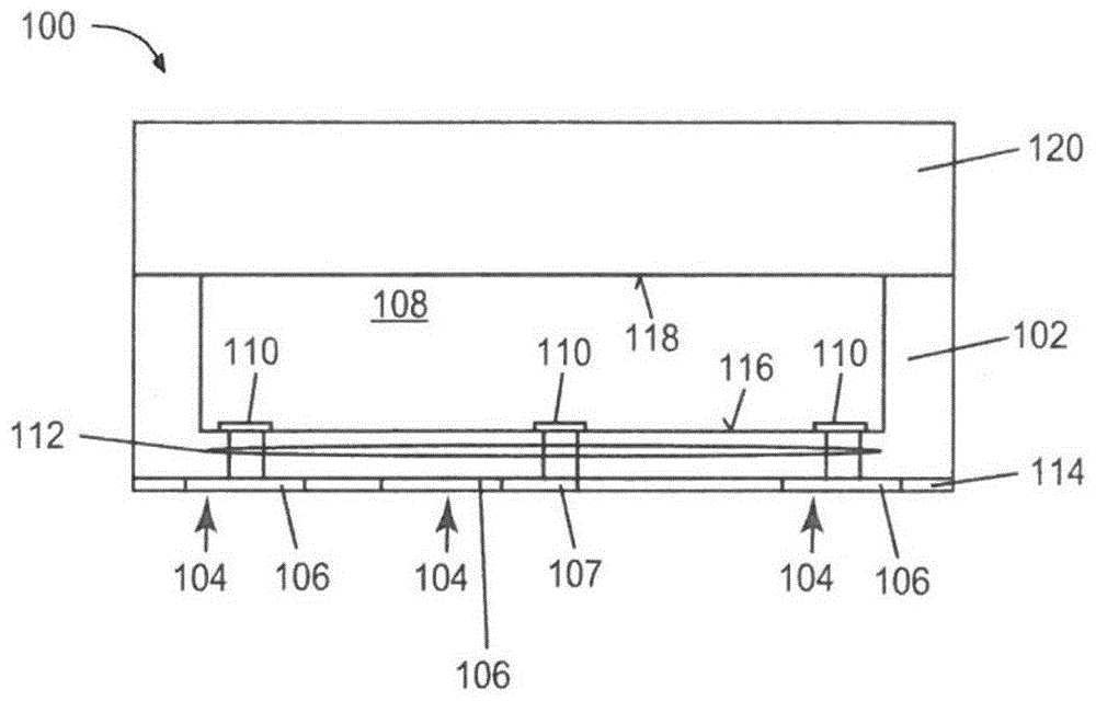
图1示出了模制封装100的实施例的截面图,并且图2示出了模制封 装100的部分平面图。模制封装100包括具有多个激光活化区104的可激 光活化模制化合物102,所述多个激光活化区104镀覆有导电材料,以在可 激光活化模制化合物102的一侧或多侧处形成金属焊盘106和/或金属迹线 107。至少一个半导体管芯108被嵌入可激光活化模制化合物102中,并且 具有多个管芯焊盘110。例如,可以仅将一个半导体管芯108嵌入可激光活 化模制化合物102中,或可以将两个或更多个半导体管芯108嵌入可激光 活化模制化合物102中。嵌入可激光活化模制化合物102中的半导体管芯 108的数量和类型取决于各种因素,并且不应被视为限制。例如,嵌入可激 光活化模制化合物102中的一个或多个半导体管芯108可以包括RF前端 电路,诸如一个或多个电源开关、RF功率放大器、LNA、天线调谐器、混 频器等。此外或替代地,嵌入可激光活化模制化合物102中的半导体管芯 108中的一个可以是电源开关,例如功率晶体管,诸如GaN晶体管或此类 功率晶体管的阵列。此外或替代地,嵌入可激光活化模制化合物102中的 一个或多个半导体管芯108可以包括逻辑器件。此外或替代地,嵌入可激 光活化模制化合物102中的半导体管芯108中的一个可以是控制器。同样, 嵌入可激光活化模制化合物102中的半导体管芯108的数量和类型取决于 各种因素,不应被视为限制。FIG. 1 shows a cross-sectional view of an embodiment of a
模制封装100还包括互连112,互连112用于将每个嵌入式半导体管芯 108的管芯焊盘110连接到形成在可激光活化模制化合物102的一侧或多 侧处的金属焊盘106和/或金属迹线107中的对应的一个。可以使用任何类 型的互连112。例如,互连112可以包括由诸如铜、金、铝、镍等的金属或 金属合金制成的线螺柱凸块,所述线螺柱凸块在第一端部处附接到管芯焊 盘110,并且在与第一端部相对的第二端部处附接到(单层)可激光活化模 制化合物102的金属焊盘106和/或金属迹线107或到多层可激光活化模制 化合物102的第一层的第一层金属结构。图3A中示出了示例性线螺柱凸块 200。在另一个实施例中,互连112包括由诸如铜、金、铝、镍等的金属或 金属合金制成的金属柱,所述金属柱在第一端部处附接到管芯焊盘110,并 且在与第一端部相对的第二端部处附接到金属焊盘106和/或金属迹线107。 图3B中示出了示例性柱202。在又一实施例中,互连112包括垂直键合线, 所述垂直键合线在第一端部处附接到管芯焊盘110,并且在与第一端部相对 的第二端部处附接到金属焊盘106和/或金属迹线107。在第一(近)端部 被键合到对应的管芯焊盘110之后,通过切割键合线以形成第二(远)端 部。键合线往往比线螺柱凸块和金属柱更薄,从而导致相邻焊盘之间更小的 电容耦合。而且,更大的长度是可能的,从而允许金属焊盘和/或金属迹线 与半导体管芯之间更大的距离。图3C中示出了示例性垂直键合线204。为 了易于说明相应的互连结构200、202、204,图3A到图3C中未示出可激 光活化模制化合物102。还可以使用其他类型的互连,例如,包括焊料凸块 的互连。如下文将进一步详细描述的,镀覆有导电材料的激光活化区104可 以位于可激光活化模制化合物102的周边以形成金属焊盘106和/或金属迹 线107,或者位于多层可激光活化模制化合物102的第一层处以形成第一层 金属结构。
模制封装100还可以包括阻焊剂层114,诸如漆、环氧树脂、液态可光 成像的焊料掩模、干膜可光成像的焊料掩模等,所述阻焊剂层114覆盖可激 光活化模制化合物102的具有金属焊盘106和/或金属迹线107的一侧的部 分,使得在该侧仅暴露金属焊盘106和/或金属迹线107的部分,以形成模 制封装100的着陆焊盘。可以通过例如焊接到印刷电路板(PCB)、另一模 制封装等制成到模制封装100的着陆焊盘的外部连接。Molded
在一个实施例中,管芯焊盘110被设置在半导体管芯的一侧116处, 并且管芯108的与第一侧116相对的第二侧118未被可激光活化模制化合 物102覆盖。相反,模制封装100还可以包括覆盖半导体管芯108的第二 侧118的顶部密封或其他类型的保护材料120。就顶部密封而言,顶部密封 充当保护半导体管芯108的包封物。顶部密封可以作为环境阻挡层、机械 增强层、防破坏层等放置在半导体管芯108之上。有两个主要类型的顶部 密封:单个材料半球状和两种材料坝填充。替代地,管芯108的与第一侧 116相对的第二侧118可以被散热器金属板覆盖。在其他实施例中,半导体 管芯108的第二侧118可以具有或可以不具有管芯焊盘110,并且至少部分 被可激光活化模制化合物102覆盖。In one embodiment, the
如本文先前所述,不必要求形成在可激光活化模制化合物102的一侧 或多侧处的金属焊盘106和/或金属迹线107位于管芯焊盘覆盖区内部。例 如,金属焊盘106的第一个106’可以由互连112电连接到管芯焊盘110的 第一个110’。第一管芯焊盘110’在图2中被示为虚线框,因为第一管芯焊 盘110’被覆盖,并且因此不在视野内。阻焊剂层114在图2中被示为部分 移除,以说明可激光活化模制化合物102的部分和具有上述第一管芯焊盘 110’的半导体管芯108的部分。在第一管芯焊盘110’的覆盖区到可激光活 化模制化合物102的具有第一金属焊盘106’的一侧上的垂直投影(从图2 中的页面出来)中,第一金属焊盘106’可以定位于第一管芯焊盘110’的覆 盖区外部。相同的第一金属焊盘106’可以在可激光活化模制化合物102的 与第一金属焊盘106’相同的一侧处连接到金属迹线107的第一个107’。在 垂直投影中,第一金属迹线107’可以被定位成至少部分在第一管芯焊盘110’ 的覆盖区内部,并且因此与第一管芯焊盘110’垂直对准。As previously described herein, it is not necessarily required that the
形成在(单层或多层)可激光活化模制化合物102的一侧或多侧处的 金属焊盘106和/或金属迹线107的大小、形状和布局取决于各种因素,并 且不应被视为限制。例如,就RF封装而言,金属焊盘106和/或金属迹线 107的厚度可以在从约10μm(微米)到约15μm的范围内。金属焊盘106 和/或金属迹线107甚至可以更薄,例如在约5μm到约10μm的范围内。 对于高功率应用(例如功率晶体管),金属焊盘106和/或金属迹线107的厚 度甚至可以更大,例如,约20μm到约40μm或甚至更厚。例如,金属焊 盘106和/或金属迹线107可以具有约1μm到约80μm的厚度。考虑到欧 姆损耗,更厚的金属焊盘106和/或金属迹线107可以是优选的,而为了保 持低电容,更薄的金属焊盘106和/或金属迹线107可以是优选的。对于不 涉及功率转换的RF应用,趋肤效应限制了更厚的金属焊盘106和/或金属 迹线107的有用性。金属焊盘106和/或金属迹线107相对于管芯焊盘110 的定位还取决于各种因素,并且不应被视为限制。The size, shape, and layout of
图4示出了模制封装300的另一实施例的平面图,所述模制封装300 具有可激光活化模制化合物102、嵌入可激光活化模制化合物102中的至少 一个半导体管芯(视野外)、以及将半导体管芯的管芯焊盘110连接到可激 光活化模制化合物102的一侧或多侧处的金属焊盘106和/或金属迹线107 的互连112。根据本实施例,在模制封装300的垂直投影(从图4的页面出 来)中,一些金属焊盘106和金属迹线107完全或部分位于相应管芯焊盘110的覆盖区内部,而其他的金属焊盘106和金属迹线107位于相应管芯焊 盘110的覆盖区外部。管芯焊盘110在图4中被示为虚线框,因为管芯焊 盘110在视野外。图4中仅标记了管芯焊盘110、互连112、金属焊盘106 和金属迹线107的单个实例,以减少附图的混淆并且有助于理解。金属焊 盘106具有大致正方形的形状,金属迹线107具有大致矩形的形状,并且 互连112具有大致圆形的形状,以在模制封装300的这些不同元件之间进 行清楚地区分。同样,形成在可激光活化模制化合物102的一侧或多侧处 的金属焊盘106和/或金属迹线107的大小、形状、布局和定位取决于各种 因素,并且不应被视为限制。互连112的大小、形状和布局也取决于各种因 素,包括互连类型(例如线螺柱凸块、金属柱、垂直键合线等),并且因此不应被视为限制。4 shows a plan view of another embodiment of a
接下来描述的是用于制造本文所述的具有可激光活化模制化合物和互 连特征的模制封装的各种方法实施例。在以下描述中,单层可激光活化模制 化合物被用作示例。然而,该描述同样适用于使用多层可激光活化模制化合 物的实施例,尤其是多层可激光活化模制化合物的第一层的实施例。Described next are various method embodiments for fabricating the molded packages described herein with laser-activatable molding compounds and interconnect features. In the following description, a single layer of laser-activatable molding compound is used as an example. However, the description is equally applicable to embodiments using multiple layers of laser-activatable molding compounds, especially embodiments of the first layer of multiple layers of laser-activatable molding compounds.
图5A到图5E示出了根据实施例的在制造本文所述的模制封装的不同 阶段期间的相应的部分截面图。5A-5E illustrate respective partial cross-sectional views during various stages of manufacturing a molded package described herein, according to an embodiment.
图5A示出了多个半导体管芯108,所述多个半导体管芯108用背离载 体400的互连112附接到诸如金属板、塑料板或膜、箔、带等的临时性载体 400。可以使用胶或双面带,例如,经由单个单元放置工艺将半导体管芯108 附接到载体400。在另一个实施例中,可以通过首先将管芯108附接到晶圆 (未示出)并且将晶圆层合到载体400,将半导体管芯108附接到载体400。5A shows a plurality of semiconductor dies 108 attached to a
如本文先前所述,每个互连112可以包括线螺柱凸块、金属柱、垂直键 合线等。在附接到载体400之前,例如通过锯切将半导体管芯108从半导 体晶圆(未示出)单个化。通常,半导体晶圆和因此所得的半导体管芯108 可以由适用于制造半导体器件的任何半导体材料制成。这样的材料的示例 包括但不限于元素半导体材料,诸如硅(Si)或锗(Ge)、IV族化合物半导 体材料(诸如碳化硅(SiC)或硅锗(SiGe))、二元、三元或四元III-V族半 导体材料,诸如氮化镓(GaN)、砷化镓(GaAs)、磷化镓(GaP)、磷化铟 (InP)、磷化铟镓(InGaP)、氮化铝镓(AlGaN)、氮化铝铟(AlInN)、氮 化铟镓(InGaN)、氮化铝镓铟(AlGaInN)或磷化铟镓砷(InGaAsP)等。As previously described herein, each
在管芯110附接到载体400之后,半导体管芯108被嵌入本文先前所 述种类的可激光活化模制化合物102中。根据本实施例,半导体管芯110被 包覆模制,因为管芯108的具有互连112的一侧被可观量的可激光活化模 制化合物102覆盖,意味着将必须减薄模制化合物102以暴露互连112。After the
图5B示出了在可激光活化模制化合物102被减薄以暴露连接到半导 体管芯108的管芯焊盘110的互连112之后的结构。在一个实施例中,通 过研磨来减薄可激光活化模制化合物102,直到暴露互连112。5B shows the structure after the laser-
图5C示出了在可激光活化模制化合物102的不同区的激光活化期间 的结构。面向下的箭头指示激光被引导到可激光活化模制化合物102的具 有暴露的互连112的一侧,由此激光活化模制化合物102的不同区104。如 本文先前所述,通过激光活化而释放的金属原子充当由激光限定的模制化 合物102的区104中的金属或金属合金(例如,Cu、Ni、NiP、Au、Cu/Ni/Au 堆叠体等)涂覆/镀覆的核心。用于可激光活化模制化合物102的这样的激 光直接结构化的适当聚合物可以包括但不限于具有树脂基底的热固性聚合 物、ABS(丙烯腈丁二烯苯乙烯)、PC/ABS(聚碳酸酯/丙烯腈丁二烯苯乙 烯)、PC(聚碳酸酯)、PA/PPA(聚酰亚胺/聚邻苯二甲酰胺)、PBT(聚对苯 二甲酸丁二醇酯)、COP(环烯烃聚合物)、PPE(聚苯醚)、LCP(液晶聚合 物)、PEI(聚氮丙啶或聚氮丙啶)、PEEK(聚醚醚酮)、PPS(聚苯硫醚)等。Figure 5C shows the structure during laser activation of different regions of the laser
图5D示出了在可激光活化模制化合物102的多个激光活化区104上 镀覆导电材料以在可激光活化模制化合物102的具有暴露的互连112的一 侧处形成金属焊盘106和/或金属迹线107之后的结构。每个互连112将对 应的管芯焊盘110电连接到用于该模制封装的对应的金属焊盘106和/或金 属迹线107。镀覆工艺可以开始于清洁步骤,以移除激光碎屑,并且接下来 可以是镀覆金属、金属合金或金属堆叠体的加法构建,以例如在Cu金属焊 盘106和/或金属迹线107的情况下,使用无电流Cu浴来形成金属焊盘106 和/或金属迹线107。如果需要更大厚度的铜,可以使用标准的电铸Cu浴。 一个或多个应用特定的涂层(诸如Ni、Au、Sn、Sn/Pb、Ag、Ag/Pd等)还 可以施加到金属焊盘106和/或金属迹线107。5D illustrates plating a conductive material over the plurality of laser-activated
图5E示出了用阻焊剂层114覆盖可激光活化模制化合物102的具有金 属焊盘106和/或金属迹线107的一侧的部分,从而仅暴露金属焊盘106和 /或金属迹线107的部分以形成每个模制封装的着陆焊盘之后的结构。阻焊 剂层114可以是漆、环氧树脂、液态可光成像的焊料掩模、干膜可光成像的 焊料掩模等。然后该结构可以重新层合到另一载体(未示出),其中着陆焊 盘面向新载体,并且可以移除旧载体。然后可以通过例如研磨在移除原始载 体的一侧处减薄该结构。顶部密封可以施加到该结构的这一侧,以保护每个 半导体管芯108的暴露的一侧。然后例如通过在邻近的封装之间穿过该结 构进行锯切来将单个的模制封装单个化。5E shows the portion of the side of the laser
图6A到图6E示出了根据另一实施例的在制造本文所述的模制封装的 不同阶段期间的相应的部分截面图。图6A到图6E中所示的实施例类似于 图5A到图5E中所示的实施例。然而,在图6A中不同的是,半导体管芯 108仅被不明显量的可激光活化模制化合物102轻微包覆模制,例如约5μm 到约20μm,这意味着可以通过对模制化合物102进行钻孔(例如,通过激 光或机械钻孔)而非研磨来暴露互连112。图6B示出了钻孔工艺之后的结 构,所述钻孔工艺在可激光活化模制化合物102中形成孔(开口)500以暴 露互连112。图6C到图6E分别与图5C到图5E相同。6A-6E illustrate respective partial cross-sectional views during different stages of manufacturing a molded package described herein, according to another embodiment. The embodiment shown in Figures 6A-6E is similar to the embodiment shown in Figures 5A-5E. Unlike in FIG. 6A , however, the semiconductor die 108 is only lightly overmolded with an insignificant amount of the laser-
图7A到图7D示出了根据又一实施例的在制造本文所述的模制封装的 不同阶段期间的相应的部分截面图。图7A到图7D中所示的实施例类似于 图5A到图5E中所示的实施例。然而,在图7A中不同的是,在可激光活 化模制化合物102中嵌入半导体管芯108和互连112之后,互连112在互 连112的背离载体400的一侧处从可激光活化模制化合物102突出。例如, 可以在用于模制该结构的夹具中放置橡胶元件。所述橡胶元件防止可激光 活化模制化合物102完全包围互连112。通过这种方式,可以避免对可激光 活化模制化合物102进行减薄(例如通过研磨)或钻孔(例如通过激光或机 械钻孔)以暴露互连112。例如,可以通过在模制工艺之后进行研磨来减薄 互连112,使得互连112与可激光活化模制化合物102上的互连112终止的 一侧是大致平面的。图7B到图7D分别与图5C到图5E相同。7A-7D illustrate respective partial cross-sectional views during different stages of manufacturing a molded package described herein, according to yet another embodiment. The embodiment shown in Figures 7A-7D is similar to the embodiment shown in Figures 5A-5E. However, in FIG. 7A , after embedding semiconductor die 108 and
如本文先前所述,在图5A-图5E、图6A-图6E和图7A-图7D中描述 的单层可激光活化模制化合物102的实施例中,互连112可以仅由线螺柱 凸块、金属柱或垂直键合线等制成。然而,在多层可激光活化模制化合物102中,互连112还包括由可激光活化模制化合物的相应层的相应层金属结 构形成的电重新分布结构。在这种情况下,延伸穿过第一层的互连112(例 如,线螺柱凸块、金属柱或垂直键合线等)可以被视为互连的初始部分,而 剩余的互连由延伸穿过多层可激光活化模制化合物102的其他层的电重新 分布结构形成。As previously described herein, in the embodiments of the single-layer laser-
图8示出了通过图5A到图5E、图6A到图6E或图7A到图7D中所 示的任何一种方法生产的模制封装600的截面图。顶部密封502覆盖半导 体管芯108的背侧118,在施加顶部密封120之前,背侧可以被减薄或可以 未被减薄。顶部密封之外的元件可以邻接半导体管芯108的背侧118。例如, 例如由金属板(未示出)形成的热沉可以附接到半导体管芯108的暴露的背侧118,或腔体可以形成在管芯背侧118处的可激光活化模制化合物102 中。Figure 8 shows a cross-sectional view of a molded
图9A到图9E、图10A到图10E、图11A到图11E以及图12A到图 12E均示出了根据额外的实施例的在制造本文描述的模制封装的不同阶段 期间的相应的部分截面图。FIGS. 9A-9E, 10A-10E, 11A-11E, and 12A-12E each illustrate respective partial cross-sections during different stages of manufacturing the molded packages described herein, according to additional embodiments. picture.
在图9A、图10A、图11A和图12A中提供了诸如金属板、塑料板或 膜、箔、带等的载体700。在图9A中,在管芯附接之前,载体700是非结 构化的。在图10A中,在管芯附接之前,载体700是结构化的。在图11A 中,载体700具有支脚702。在图12A中,在管芯附接之前,将间隔体材料 704施加到载体700。间隔体材料704允许在管芯的背侧处有特定的绝缘距 离。例如就MEMS(微机电系统)或传感器应用而言,稍后可以移除间隔 体材料704以形成腔体,或者用管芯的背侧处的热沉来替换间隔体材料704。 间隔体材料704还提供了缓冲,使得管芯不会与随后用于移除载体的化学 物质接触。A
图9B、图10B、图11B和图12B示出了在使用诸如焊料、粘合带、胶 等管芯附接材料706来附接半导体管芯108之后的相应载体。就图12B而 言,间隔体材料704可以充当管芯附接材料。Figures 9B, 10B, 11B, and 12B illustrate the respective carriers after the semiconductor die 108 has been attached using a die attach
图9C、图10C、图11C和图12C示出了在用可激光活化模制化合物 102来模制半导体管芯108之后的相应结构,并且可以对应于本文先前结合 图5A-图5B、图6A-图6B和图7A所述的任何实施例。即,可以通过减薄 (例如,通过研磨)可激光活化模制化合物102(例如,图5B)、对可激光 活化模制化合物102进行钻孔(例如,通过激光或机械钻孔)(例如,图6B)、或通过修改模制夹具以使得互连112从可激光活化模制化合物102突出而 无需对模制化合物102进行减薄或激光钻孔(例如,图7A)来暴露管芯互 连112。FIGS. 9C, 10C, 11C, and 12C illustrate the corresponding structures after molding the semiconductor die 108 with the laser-
图9D、图10D、图11D和图12D示出了在激光活化可激光活化模制化 合物的不同区并且在可激光活化模制化合物的激光活化区上镀覆导电材料 以形成金属焊盘106和/或金属迹线107之后的相应结构,并且可以对应于 本文先前结合图5C-图5D、图6C-图6D和图7B-图7C所述的任何实施例。Figures 9D, 10D, 11D, and 12D illustrate laser activation of different regions of the laser-activatable molding compound and plating conductive material on the laser-activated regions of the laser-activatable molding compound to form
图9E、10E、11E和12E示出了在(任选的)移除载体700之后的相应 结构。就图9E而言,半导体管芯108的背侧或管芯背侧处的管芯附接材料 706(如果未移除)被暴露,并且与可激光活化模制化合物102的背侧是大 致平面的。如下文将要更详细所述,载体700也可以保留在可激光活化模 制化合物102的背侧,尤其是如果载体700被形成为热沉(例如,金属板) 和/或管芯108为功率管芯(例如,功率晶体管)。就图10E而言,管芯焊盘 (未示出)设置在每个管芯108的第一侧处,每个管芯108的(相对的)第 二侧不被可激光活化模制化合物102覆盖,可激光活化模制化合物102比 半导体管芯108更厚,并且可激光活化模制化合物102在半导体管芯108 的通过移除结构化载体700而形成的第二侧处具有凹陷区708。例如,对于 MEMS或传感器应用而言,凹陷区708可以用热沉材料填充,或者可以保 持不填充,以形成腔体。就图11E而言,由于使用了支脚702,可激光活化 模制化合物102在管芯108的周边周围接触管芯108的背侧。支脚702可 以保留在最终模制封装中,或者可以被移除,例如,以形成相应腔体。就图 12E而言,间隔体材料704可以保留在最终模制封装中,或者可以被移除, 例如,以形成相应腔体。Figures 9E, 10E, 11E and 12E show the corresponding structures after (optional) removal of
图13示出了在镀覆工艺之后和载体移除之前通过图9A到图9E、图 10A到图10E、图11A到图11E和图12A到图12E中所示的任何一种方法 来生产的结构的部分平面图。在单个化之前,对于若干封装而言,金属焊盘 106和/或金属迹线107是可见的。图13中仅标记了金属焊盘106/金属迹线 107的单个实例,以减少附图的混淆并且有助于理解。FIG. 13 shows a method produced by any of the methods shown in FIGS. 9A-9E, 10A-10E, 11A-11E, and 12A-12E after the plating process and before carrier removal. Partial floor plan of the structure. Prior to singulation,
图14示出了在镀覆工艺之后和载体移除之前,贯穿通过图9A到图9E、 图10A到图10E、图11A到图11E和图12A到图12E中所示的任何一种方 法来生产的一个互连112、一个管芯焊盘110和一个金属焊盘/金属迹线 106/107的截面图。一个或多个应用特定的涂层800(诸如Ni、Au、Sn、 Sn/Pb、Ag、Ag/Pd等)可以施加到互连112,如图14中所示。Figure 14 shows the process through any of the methods shown in Figures 9A-9E, 10A-10E, 11A-11E, and 12A-12E after the plating process and before carrier removal. Cross-sectional view of one
图15A示出了附接到载体400的半导体管芯108。在这种情况下,载 体400是永久载体,例如,充当热沉的金属板。半导体管芯108例如可以 是功率管芯。例如,半导体管芯108可以是(仅)在其上表面具有管芯焊盘 110的水平半导体器件。例如,半导体管芯108可以是在其上表面具有源极 (S)管芯焊盘110、栅极(G)管芯焊盘110和漏极(D)管芯焊盘110的 功率晶体管(例如,GaN功率晶体管,或者尤其是功率GaN HEMT(高电 子迁移率晶体管))。FIG. 15A shows semiconductor die 108 attached to
半导体管芯108可以导电附接(例如,焊接)到永久载体400。此外, 金属条1510可以导电附接到永久载体400。Semiconductor die 108 may be conductively attached (eg, soldered) to
图15B示出了将管芯互连112(包括例如线螺柱凸块、金属柱、垂直键 合线等)附接到半导体管芯108的管芯焊盘110上。15B illustrates the attachment of die interconnects 112 (including, for example, wire stud bumps, metal posts, vertical bond wires, etc.) to die
图15C示出了将半导体管芯108和互连112嵌入在(第一)可激光活 化模制化合物102中,参见上文的描述。Figure 15C shows embedding of semiconductor die 108 and
图15D示出了在背离载体400的一侧处暴露互连112(参见图15D中 最上方图示)。如更早所述,这可以包括例如减薄或钻孔。此外,图15D示 出了可激光活化模制化合物102的多个区的激光活化。在下文中也将激光 活化称为激光直接结构化(LDS)。在这种情况下,LDS用于生成充当源极 (S)、栅极(G)和漏极(D)区的激光活化区104。此外,图15D示出了 用导电材料镀覆激光活化区104以形成金属焊盘106,在这种情况下为源极 (S)、漏极(D)和栅极(G)金属焊盘106。金属焊盘106电连接到互连 112。如更早所述,镀覆可以包括Cu和/或NiP和/或Au镀覆。Figure 15D shows
图15E示出了如更早所述用抗蚀剂层114部分掩蔽金属焊盘106。Figure 15E shows
参考图15F,如更早所述,然后可以例如通过在邻近封装之间穿过该结 构进行锯切来单个化单个的模制封装。Referring to Figure 15F, as described earlier, the individual molded packages may then be singulated, for example, by sawing through the structure between adjacent packages.
图16示出了半导体管芯108上的平面图。半导体管芯108是水平功率 晶体管,例如GaN晶体管。如从图16显而易见的是,半导体管芯108的管 芯焊盘110被设计为例如交替的漏极(D)和源极(S)焊盘以及一个栅极 (G)焊盘。FIG. 16 shows a plan view on
在这些和其他情况下,互连还可以包括互连形成在可激光活化模制化 合物102上的管芯焊盘110和金属焊盘106和/或金属迹线107的电重新分 布结构。为此,可激光活化模制化合物102可以形成为多层模制化合物。如 下文更详细所述,在制造多层模制化合物封装的工艺期间,多层模制化合物 的每层被单个模制、激光活化和镀覆。In these and other cases, the interconnects may also include electrical redistribution structures interconnecting
参考图17A,诸如图16中所示的半导体管芯108的半导体管芯附接到 例如是永久载体400的载体400。包括例如线螺柱凸块或金属柱或垂直键合 线的互连的初始部分已经被附接到半导体管芯108的多个管芯焊盘110。如 更早所述,管芯附接材料706可以用于将半导体管芯108附接到永久载体 400。此外,金属条1510可以附接到永久载体400。金属条1510(例如,由 Cu制成)可以在永久载体400(例如,用于顶侧冷却的热沉金属板)和模 制化合物102的上表面处的镀覆I/O(输入/输出)之间电互连和热互连。Referring to FIG. 17A , a semiconductor die, such as semiconductor die 108 shown in FIG. 16 , is attached to a
替代地,参见图17B,在已经将半导体管芯108附接到载体400之后, 可以将互连的初始部分(例如,线螺柱凸块或金属柱或垂直键合线)附接到 半导体管芯108的多个管芯焊盘110。在图17A和图17B的示例中,金属 柱202被用作示例以说明互连的初始部分。Alternatively, referring to FIG. 17B, after the semiconductor die 108 has been attached to the
参考图17C,将半导体管芯108和互连的初始部分(例如,柱202), 以及任选的永久载体400嵌入可激光活化模制化合物102的第一层102_1 中。该工艺与结合图15C所述的工艺相同。此外,可以将例如减薄或钻孔 的工艺施加到可激光活化模制化合物102的第一层102_1,以暴露互连的初 始部分。Referring to FIG. 17C , semiconductor die 108 and initial portions of interconnects (eg, pillars 202 ), and optional
参考图17D,将激光引导到可激光活化模制化合物102的第一层102_1, 以激光活化可激光活化模制化合物102的第一层102_1的多个区。在该LDS 工艺之后,接着是在可激光活化模制化合物102的第一层102_1的多个激 光活化区上镀覆导电材料,以在可激光活化模制化合物102的第一层102_1 的表面处形成第一层金属结构1710_1、1720_1、1730_1。在图17D的示例 中,第一层金属结构1710_1连接到半导体管芯108的源极(S),第一层金 属结构1720_1连接到漏极(D),并且第一层金属结构1730_1连接到栅极 (G)。Referring to FIG. 17D , a laser is directed to the first layer 102_1 of the laser
参考图17E,在可激光活化模制化合物102的第一层102_1的表面之 上施加可激光活化模制化合物102的第二层102_2。17E, a second layer 102_2 of laser
参考图17F,对于可激光活化模制化合物102的第二层102_2执行(例 如,第二)LDS工艺接着是镀覆工艺,以在可激光活化模制化合物102的 第二层102_2的表面处形成第二层金属结构1710_2、1720_2和1730_2。17F , a (eg, a second) LDS process followed by a plating process is performed on the second layer 102_2 of the laser
参考图17G,可以在可激光活化模制化合物102的第二层102_2上执 行附加的(例如,第三)LDS工艺和附加的镀覆工艺。在本示例中,该附加 的LDS工艺和附加的镀覆工艺提供用于分别将第二层金属结构1710_2、 1720_2、1730_2改型为第二层金属结构1710_2’、1720_2’和1730_2’。17G, additional (e.g., third) LDS processes and additional plating processes may be performed on the second layer 102_2 of the laser-
参考图17H,可以在可激光活化模制化合物102的第二层102_2的表 面之上施加可激光活化模制化合物102的第三层102_3。所有模制化合物层 102_1、102_2、102_3可以在具有单个(逐渐增大的)模制腔体尺寸的单个 模制工具中被施加。17H, a third layer 102_3 of laser
图17I示出了施加到第三层102_3以在可激光活化模制化合物102的 第三层102_3的表面处形成第三层金属结构1710_3、1720_3和1730_3的 另一(例如第四)LDS工艺和镀覆工艺。参考以上对应的描述以避免重复。17I illustrates another (eg, fourth) LDS process applied to third layer 102_3 to form third layer metal structures 1710_3, 1720_3, and 1730_3 at the surface of third layer 102_3 of laser-
然后,如图17J所示,可以施加另一(例如,第五)LDS和镀覆工艺, 以将第三层金属结构1710_3、1720_3、1730_3分别改型为改型的第三层金 属结构1710_3’、1720_3’和1730_3’。Then, as shown in FIG. 17J, another (eg, fifth) LDS and plating process may be applied to modify the third-level metal structures 1710_3, 1720_3, 1730_3, respectively, into modified third-level metal structures 1710_3' , 1720_3' and 1730_3'.
换言之,对于多层可激光活化模制化合物102而言,每层可以由LDS 和镀覆单独地模制和处理。此外,可以将一种或多种LDS工艺和镀覆工艺 施加到可激光活化模制化合物102的每个层102_1、102_2、102_3。在本示 例中,将一种LDS和金属镀覆工艺施加到第一层102_1,将两种LDS和镀 覆工艺施加到第二层102_2,并将两种LDS和金属镀覆工艺施加到第三层 102_3。In other words, for multiple layers of laser-
以下步骤可以包括如更早分别结合图15E和图15F所述的掩蔽和单个 化。The following steps may include masking and singulation as described earlier in connection with Figures 15E and 15F, respectively.
图18示出了通过例如图17A到图17J中举例说明的方法来制造的模制 的多层封装1800的透视截面图。从图18显而易见的是,第一层和第二层 以及第三层金属结构提供了镀覆的电重新分布层,所述电重新分布层提供 了高灵活性,以将半导体管芯108的管芯焊盘110的图案转换成模制化合 物102的表面处的金属焊盘106和/或金属迹线107的期望图案。Figure 18 shows a perspective cross-sectional view of a molded
即,可以通过层模制、LDS和镀覆工艺容易地改变互连设计,并且这 种灵活性包括电重新分布层的修改以及I/O覆盖区布局的任何重新设计(例 如,代表模制封装1800的外部端子焊盘的金属焊盘106和/或金属迹线107 的重新设计)。此外,生成了无应力互连,因为互连是通过在可镀覆模制化 合物上进行(例如,电流)镀覆来形成的。还要指出的是,通过LDS和镀 覆形成电重新分布层是无掩模工艺,即,避免了使用掩模对互连进行结构化 的必要性。That is, interconnect design can be easily changed through layer molding, LDS, and plating processes, and this flexibility includes modification of electrical redistribution layers and any redesign of I/O footprint layout (eg, representative of molded packages Redesign of
图19是图18中所示的模制封装1800的分解图。在本示例中,由第三 层金属结构1710_3’实现源极(S)金属焊盘106,由第三层金属结构1720_3’ 实现漏极(D)金属焊盘106,并且由第三层金属结构1730_3’实现栅极(G) 金属焊盘106。FIG. 19 is an exploded view of the molded
诸如“第一”、“第二”等的术语用于描述各种元件、区、部分等,并且 也并非旨在限制。贯穿说明书中相似的术语指示相似的元件。Terms such as "first", "second", and the like, are used to describe various elements, regions, sections, etc. and are also not intended to be limiting. Similar terms refer to similar elements throughout the specification.
如本文所用,术语“具有”、“包含”、“包括”等是开放式术语,表示存 在所述元件或特征,但不排除额外的元件或特征。冠词“一个”和“所述” 旨在包括复数和单数,除非上下文另外明确指出。As used herein, the terms "having", "comprising", "including" and the like are open-ended terms that indicate the presence of stated elements or features, but do not exclude additional elements or features. The articles "a" and "said" are intended to include both the plural and the singular unless the context clearly dictates otherwise.
尽管本文已经说明和描述了特定的实施例,但本领域的普通技术人员 将认识到,在不脱离本发明的范围的情况下,可以用多种替代和/或等价实 施方式代替所示和所述的特定实施例。本申请旨在覆盖本文所讨论的特定 实施例的任何修改或变化。因此,旨在使本发明仅受到权利要求及其等同物 的限制。While specific embodiments have been illustrated and described herein, those of ordinary skill in the art will recognize that various alternative and/or equivalent embodiments may be substituted for those shown and/or equivalents without departing from the scope of the invention. specific examples described. This application is intended to cover any adaptations or variations of the specific embodiments discussed herein. Therefore, it is intended that this invention be limited only by the claims and their equivalents.
Claims (16)
Applications Claiming Priority (4)
| Application Number | Priority Date | Filing Date | Title |
|---|---|---|---|
| EP19177680.6 | 2019-05-31 | ||
| EP19177680 | 2019-05-31 | ||
| EP19181649.5 | 2019-06-21 | ||
| EP19181649.5A EP3754691A1 (en) | 2019-06-21 | 2019-06-21 | Semiconductor package having a laser-activatable mold compound |
Publications (1)
| Publication Number | Publication Date |
|---|---|
| CN112018052A true CN112018052A (en) | 2020-12-01 |
Family
ID=73507052
Family Applications (1)
| Application Number | Title | Priority Date | Filing Date |
|---|---|---|---|
| CN202010448139.8A Pending CN112018052A (en) | 2019-05-31 | 2020-05-25 | Semiconductor package with laser activatable molding compound |
Country Status (2)
| Country | Link |
|---|---|
| US (1) | US11289436B2 (en) |
| CN (1) | CN112018052A (en) |
Cited By (5)
| Publication number | Priority date | Publication date | Assignee | Title |
|---|---|---|---|---|
| CN112885727A (en) * | 2021-01-19 | 2021-06-01 | 济南南知信息科技有限公司 | Chip integrated circuit package and manufacturing method thereof |
| CN112885726A (en) * | 2021-01-19 | 2021-06-01 | 济南南知信息科技有限公司 | Intelligent power chip structure and manufacturing method thereof |
| CN113078118A (en) * | 2021-03-25 | 2021-07-06 | 福唐激光(苏州)科技有限公司 | Method for realizing POP (point of presence protocol) connection by laser and POP structure thereof |
| CN115295426A (en) * | 2021-05-04 | 2022-11-04 | 星科金朋私人有限公司 | Semiconductor device and method for embedding circuit pattern in package for system-in-package module |
| WO2024098355A1 (en) * | 2022-11-11 | 2024-05-16 | Innoscience (suzhou) Semiconductor Co., Ltd. | Nitride-based semiconductor circuit and method for manufacturing the same |
Families Citing this family (7)
| Publication number | Priority date | Publication date | Assignee | Title |
|---|---|---|---|---|
| CN113491007A (en) * | 2019-03-11 | 2021-10-08 | Hrl实验室有限责任公司 | Method of protecting die during Metal Embedded Chip Assembly (MECA) processing |
| US11552024B2 (en) | 2019-08-16 | 2023-01-10 | Stmicroelectronics S.R.L. | Method of manufacturing quad flat no-lead semiconductor devices and corresponding quad flat no-lead semiconductor device |
| US11521861B2 (en) * | 2019-08-16 | 2022-12-06 | Stmicroelectronics S.R.L. | Method of manufacturing semiconductor devices and corresponding semiconductor device |
| CN216902917U (en) | 2020-12-17 | 2022-07-05 | 意法半导体股份有限公司 | Multi-die semiconductor device |
| US12080631B2 (en) | 2021-08-31 | 2024-09-03 | Stmicroelectronics S.R.L. | Leadframe-less laser direct structuring (LDS) package |
| US20230170329A1 (en) * | 2021-11-29 | 2023-06-01 | Infineon Technologies Ag | Semiconductor package with metal posts from structured leadframe |
| US20230197585A1 (en) * | 2021-12-20 | 2023-06-22 | Infineon Technologies Ag | Semiconductor package interconnect and power connection by metallized structures on package body |
Citations (6)
| Publication number | Priority date | Publication date | Assignee | Title |
|---|---|---|---|---|
| CN101930958A (en) * | 2010-07-08 | 2010-12-29 | 日月光半导体制造股份有限公司 | Semiconductor package and manufacturing method thereof |
| CN103222051A (en) * | 2010-11-18 | 2013-07-24 | 密克罗奇普技术公司 | Using Bump Bonding to Distribute Current Flow on Semiconductor Power Devices |
| US20150279778A1 (en) * | 2014-03-28 | 2015-10-01 | Stats Chippac, Ltd. | Semiconductor Device and Method of Forming RDL and Vertical Interconnect by Laser Direct Structuring |
| CN105448875A (en) * | 2014-09-18 | 2016-03-30 | 英飞凌科技奥地利有限公司 | Electronic component |
| CN206364003U (en) * | 2016-01-20 | 2017-07-28 | 苹果公司 | Packaging, system in package device and electronic equipment |
| US20180342434A1 (en) * | 2017-05-23 | 2018-11-29 | Stmicroelectronics S.R.L. | Method of manufacturing semiconductor devices and corresponding semiconductor device |
Family Cites Families (61)
| Publication number | Priority date | Publication date | Assignee | Title |
|---|---|---|---|---|
| JP2931936B2 (en) | 1992-01-17 | 1999-08-09 | 株式会社日立製作所 | Method for manufacturing lead frame for semiconductor device, lead frame for semiconductor device, and resin-sealed semiconductor device |
| JPH0685161A (en) | 1992-09-07 | 1994-03-25 | Hitachi Ltd | High density package type semiconductor device |
| KR970010678B1 (en) | 1994-03-30 | 1997-06-30 | 엘지반도체 주식회사 | Lead frame and the package thereof |
| KR0134648B1 (en) | 1994-06-09 | 1998-04-20 | 김광호 | Low Noise Multilayer Chip Package |
| US5729433A (en) | 1996-01-30 | 1998-03-17 | Micromodule Systems, Inc. | Multiple chip module assembly for top of mother board |
| JPH09260568A (en) | 1996-03-27 | 1997-10-03 | Mitsubishi Electric Corp | Semiconductor device and manufacturing method thereof |
| JPH10242360A (en) | 1997-02-25 | 1998-09-11 | Oki Electric Ind Co Ltd | Semiconductor device |
| SG75958A1 (en) | 1998-06-01 | 2000-10-24 | Hitachi Ulsi Sys Co Ltd | Semiconductor device and a method of producing semiconductor device |
| US6424031B1 (en) | 2000-05-08 | 2002-07-23 | Amkor Technology, Inc. | Stackable package with heat sink |
| US6534876B1 (en) | 2000-06-30 | 2003-03-18 | Amkor Technology, Inc. | Flip-chip micromachine package |
| US7633765B1 (en) | 2004-03-23 | 2009-12-15 | Amkor Technology, Inc. | Semiconductor package including a top-surface metal layer for implementing circuit features |
| US6873039B2 (en) | 2002-06-27 | 2005-03-29 | Tessera, Inc. | Methods of making microelectronic packages including electrically and/or thermally conductive element |
| US8169062B2 (en) | 2002-07-02 | 2012-05-01 | Alpha And Omega Semiconductor Incorporated | Integrated circuit package for semiconductior devices with improved electric resistance and inductance |
| US20040061213A1 (en) | 2002-09-17 | 2004-04-01 | Chippac, Inc. | Semiconductor multi-package module having package stacked over die-up flip chip ball grid array package and having wire bond interconnect between stacked packages |
| JP3574450B1 (en) | 2003-05-16 | 2004-10-06 | 沖電気工業株式会社 | Semiconductor device and method of manufacturing semiconductor device |
| SG120123A1 (en) | 2003-09-30 | 2006-03-28 | Micron Technology Inc | Castellated chip-scale packages and methods for fabricating the same |
| KR20070116097A (en) | 2005-03-16 | 2007-12-06 | 야마하 가부시키가이샤 | Semiconductor device, manufacturing method of semiconductor device, and cover frame |
| JP2008544867A (en) | 2005-06-30 | 2008-12-11 | コーニンクレッカ フィリップス エレクトロニクス エヌ ヴィ | Manufacturing method of MEMS element |
| US7378300B2 (en) | 2005-09-22 | 2008-05-27 | Stats Chippac Ltd. | Integrated circuit package system |
| US7494920B2 (en) | 2005-10-14 | 2009-02-24 | Honeywell International Inc. | Method of fabricating a vertically mountable IC package |
| US7629675B2 (en) | 2006-05-03 | 2009-12-08 | Marvell International Technology Ltd. | System and method for routing signals between side-by-side die in lead frame type system in a package (SIP) devices |
| US7829998B2 (en) | 2007-05-04 | 2010-11-09 | Stats Chippac, Ltd. | Semiconductor wafer having through-hole vias on saw streets with backside redistribution layer |
| US7723159B2 (en) | 2007-05-04 | 2010-05-25 | Stats Chippac, Ltd. | Package-on-package using through-hole via die on saw streets |
| US7944034B2 (en) | 2007-06-22 | 2011-05-17 | Texas Instruments Incorporated | Array molded package-on-package having redistribution lines |
| US7843046B2 (en) | 2008-02-19 | 2010-11-30 | Vertical Circuits, Inc. | Flat leadless packages and stacked leadless package assemblies |
| US7868442B2 (en) | 2008-06-30 | 2011-01-11 | Headway Technologies, Inc. | Layered chip package and method of manufacturing same |
| US7863722B2 (en) | 2008-10-20 | 2011-01-04 | Micron Technology, Inc. | Stackable semiconductor assemblies and methods of manufacturing such assemblies |
| WO2010080068A1 (en) | 2009-01-12 | 2010-07-15 | Ravi Kanth Kolan | Method for manufacturing a low cost three dimensional stack package and resulting structures using through silicon vias and assemblies |
| US20100207257A1 (en) | 2009-02-17 | 2010-08-19 | Advanced Semiconductor Engineering, Inc. | Semiconductor package and manufacturing method thereof |
| US8026589B1 (en) | 2009-02-23 | 2011-09-27 | Amkor Technology, Inc. | Reduced profile stackable semiconductor package |
| US9087850B2 (en) | 2009-07-06 | 2015-07-21 | Renesas Electronics Corporation | Method for manufacturing semiconductor device |
| US20110095417A1 (en) * | 2009-10-28 | 2011-04-28 | Fairchild Semiconductor Corporation | Leadless semiconductor device terminal |
| US9230883B1 (en) | 2010-01-20 | 2016-01-05 | Amkor Technology, Inc. | Trace stacking structure and method |
| US9196509B2 (en) | 2010-02-16 | 2015-11-24 | Deca Technologies Inc | Semiconductor device and method of adaptive patterning for panelized packaging |
| KR20120056624A (en) | 2010-11-25 | 2012-06-04 | 하나 마이크론(주) | Semiconductor package |
| US8623702B2 (en) | 2011-02-24 | 2014-01-07 | Stats Chippac, Ltd. | Semiconductor device and method of forming conductive THV and RDL on opposite sides of semiconductor die for RDL-to-RDL bonding |
| US8525344B2 (en) | 2011-02-24 | 2013-09-03 | Stats Chippac, Ltd. | Semiconductor device and method of forming bond wires between semiconductor die contact pads and conductive TOV in peripheral area around semiconductor die |
| US20130050227A1 (en) | 2011-08-30 | 2013-02-28 | Qualcomm Mems Technologies, Inc. | Glass as a substrate material and a final package for mems and ic devices |
| US20130154106A1 (en) | 2011-12-14 | 2013-06-20 | Broadcom Corporation | Stacked Packaging Using Reconstituted Wafers |
| US8759956B2 (en) | 2012-07-05 | 2014-06-24 | Infineon Technologies Ag | Chip package and method of manufacturing the same |
| US9224688B2 (en) | 2013-01-04 | 2015-12-29 | Taiwan Semiconductor Manufacturing Company, Ltd. | Metal routing architecture for integrated circuits |
| US9576932B2 (en) | 2013-03-09 | 2017-02-21 | Adventive Ipbank | Universal surface-mount semiconductor package |
| JP2016516279A (en) | 2013-03-15 | 2016-06-02 | セルガード エルエルシー | Multilayer hybrid battery separator for lithium ion secondary battery and method for producing the same |
| JP2014220439A (en) | 2013-05-10 | 2014-11-20 | ルネサスエレクトロニクス株式会社 | Method of manufacturing semiconductor device and semiconductor device |
| US9559064B2 (en) | 2013-12-04 | 2017-01-31 | Taiwan Semiconductor Manufacturing Company, Ltd. | Warpage control in package-on-package structures |
| US9589900B2 (en) | 2014-02-27 | 2017-03-07 | Taiwan Semiconductor Manufacturing Company, Ltd. | Metal pad for laser marking |
| US20160005675A1 (en) | 2014-07-07 | 2016-01-07 | Infineon Technologies Ag | Double sided cooling chip package and method of manufacturing the same |
| US9564409B2 (en) | 2015-01-27 | 2017-02-07 | Semiconductor Components Industries, Llc | Methods of forming semiconductor packages with an intermetallic layer comprising tin and at least one of silver, copper or nickel |
| US10264664B1 (en) | 2015-06-04 | 2019-04-16 | Vlt, Inc. | Method of electrically interconnecting circuit assemblies |
| US9806043B2 (en) | 2016-03-03 | 2017-10-31 | Infineon Technologies Ag | Method of manufacturing molded semiconductor packages having an optical inspection feature |
| DE102016103790B8 (en) | 2016-03-03 | 2021-06-02 | Infineon Technologies Ag | Production of a package using a platable encapsulation material |
| US10056319B2 (en) | 2016-04-29 | 2018-08-21 | Delta Electronics, Inc. | Power module package having patterned insulation metal substrate |
| CN108022899B (en) | 2016-10-28 | 2020-02-11 | 台达电子工业股份有限公司 | Power module having lead member and method of manufacturing the same |
| US10217728B2 (en) | 2016-11-22 | 2019-02-26 | Advanced Semiconductor Engineering, Inc. | Semiconductor package and semiconductor process |
| US10607977B2 (en) | 2017-01-20 | 2020-03-31 | Google Llc | Integrated DRAM with low-voltage swing I/O |
| MY202342A (en) | 2017-06-08 | 2024-04-24 | Intel Corp | Over-molded ic package with in-mold capacitor |
| US10818578B2 (en) | 2017-10-12 | 2020-10-27 | Stmicroelectronics S.R.L. | Method of manufacturing semiconductor devices, corresponding device and circuit |
| US10741466B2 (en) | 2017-11-17 | 2020-08-11 | Infineon Technologies Ag | Formation of conductive connection tracks in package mold body using electroless plating |
| IT201800002903A1 (en) | 2018-02-21 | 2019-08-21 | St Microelectronics Srl | PROCEDURE FOR MANUFACTURING SEMICONDUCTOR DEVICES AND CORRESPONDING SEMICONDUCTOR DEVICE |
| US20200185293A1 (en) | 2018-12-07 | 2020-06-11 | Infineon Technologies Ag | Semiconductor Package Having a Laser-Activatable Mold Compound |
| IT201800020998A1 (en) | 2018-12-24 | 2020-06-24 | St Microelectronics Srl | Process for manufacturing semiconductor devices and corresponding semiconductor device |
-
2020
- 2020-05-25 CN CN202010448139.8A patent/CN112018052A/en active Pending
- 2020-05-28 US US16/886,305 patent/US11289436B2/en active Active
Patent Citations (6)
| Publication number | Priority date | Publication date | Assignee | Title |
|---|---|---|---|---|
| CN101930958A (en) * | 2010-07-08 | 2010-12-29 | 日月光半导体制造股份有限公司 | Semiconductor package and manufacturing method thereof |
| CN103222051A (en) * | 2010-11-18 | 2013-07-24 | 密克罗奇普技术公司 | Using Bump Bonding to Distribute Current Flow on Semiconductor Power Devices |
| US20150279778A1 (en) * | 2014-03-28 | 2015-10-01 | Stats Chippac, Ltd. | Semiconductor Device and Method of Forming RDL and Vertical Interconnect by Laser Direct Structuring |
| CN105448875A (en) * | 2014-09-18 | 2016-03-30 | 英飞凌科技奥地利有限公司 | Electronic component |
| CN206364003U (en) * | 2016-01-20 | 2017-07-28 | 苹果公司 | Packaging, system in package device and electronic equipment |
| US20180342434A1 (en) * | 2017-05-23 | 2018-11-29 | Stmicroelectronics S.R.L. | Method of manufacturing semiconductor devices and corresponding semiconductor device |
Cited By (6)
| Publication number | Priority date | Publication date | Assignee | Title |
|---|---|---|---|---|
| CN112885727A (en) * | 2021-01-19 | 2021-06-01 | 济南南知信息科技有限公司 | Chip integrated circuit package and manufacturing method thereof |
| CN112885726A (en) * | 2021-01-19 | 2021-06-01 | 济南南知信息科技有限公司 | Intelligent power chip structure and manufacturing method thereof |
| CN112885726B (en) * | 2021-01-19 | 2022-03-25 | 杭州梵特斯科技有限公司 | Intelligent power chip structure and manufacturing method thereof |
| CN113078118A (en) * | 2021-03-25 | 2021-07-06 | 福唐激光(苏州)科技有限公司 | Method for realizing POP (point of presence protocol) connection by laser and POP structure thereof |
| CN115295426A (en) * | 2021-05-04 | 2022-11-04 | 星科金朋私人有限公司 | Semiconductor device and method for embedding circuit pattern in package for system-in-package module |
| WO2024098355A1 (en) * | 2022-11-11 | 2024-05-16 | Innoscience (suzhou) Semiconductor Co., Ltd. | Nitride-based semiconductor circuit and method for manufacturing the same |
Also Published As
| Publication number | Publication date |
|---|---|
| US11289436B2 (en) | 2022-03-29 |
| US20200381380A1 (en) | 2020-12-03 |
Similar Documents
| Publication | Publication Date | Title |
|---|---|---|
| CN112018052A (en) | Semiconductor package with laser activatable molding compound | |
| CN111293088A (en) | Semiconductor package with laser activatable molding compound | |
| US9607966B2 (en) | Chip arrangement | |
| US10861760B2 (en) | Method of manufacturing semiconductor devices and corresponding semiconductor device | |
| US20130181332A1 (en) | Package leadframe for dual side assembly | |
| US12176222B2 (en) | Semiconductor package with metal posts from structured leadframe | |
| US20190139883A1 (en) | Packaged semiconductor system having unidirectional connections to discrete components | |
| CN113826196B (en) | Double-sided cooled electronic device | |
| CN116403985A (en) | Method of forming packaged semiconductor device and packaged semiconductor device | |
| CN104517905A (en) | Metal redistribution layer for molded substrates | |
| US11984388B2 (en) | Semiconductor package structures and methods of manufacture | |
| US7923847B2 (en) | Semiconductor system-in-a-package containing micro-layered lead frame | |
| EP3754691A1 (en) | Semiconductor package having a laser-activatable mold compound | |
| US20230170329A1 (en) | Semiconductor package with metal posts from structured leadframe | |
| KR20120018756A (en) | Leadframe for ic package and method of manufacture | |
| US20100140773A1 (en) | Stacked chip, micro-layered lead frame semiconductor package | |
| EP4546399A1 (en) | Molded power package with vertical interconnect | |
| CN114551402A (en) | Semiconductor package including electrical redistribution layers of different thicknesses and method of manufacturing the same | |
| US20060134836A1 (en) | Method of marking a low profile packaged semiconductor device | |
| US20240312956A1 (en) | Subtractive Metal Structuring on Surface of Semiconductor Package | |
| US20250293217A1 (en) | Embedded package with stacked semiconductor dies | |
| US12500197B2 (en) | Encapsulant-defined land grid array (LGA) package and method for making the same | |
| US20240030113A1 (en) | Quad flat no-lead (qfn) package without leadframe and direct contact interconnect build-up structure | |
| CN116435284A (en) | Semiconductor packaging substrate made of non-metallic material and manufacturing method thereof | |
| CN120261289A (en) | Embedded power semiconductor package with sidewall contacts |
Legal Events
| Date | Code | Title | Description |
|---|---|---|---|
| PB01 | Publication | ||
| PB01 | Publication | ||
| SE01 | Entry into force of request for substantive examination | ||
| SE01 | Entry into force of request for substantive examination |