CN112015012A - Liquid crystal display device having a plurality of pixel electrodes - Google Patents
Liquid crystal display device having a plurality of pixel electrodes Download PDFInfo
- Publication number
- CN112015012A CN112015012A CN202010469569.8A CN202010469569A CN112015012A CN 112015012 A CN112015012 A CN 112015012A CN 202010469569 A CN202010469569 A CN 202010469569A CN 112015012 A CN112015012 A CN 112015012A
- Authority
- CN
- China
- Prior art keywords
- liquid crystal
- pixel
- sub
- alignment
- alignment film
- Prior art date
- Legal status (The legal status is an assumption and is not a legal conclusion. Google has not performed a legal analysis and makes no representation as to the accuracy of the status listed.)
- Granted
Links
Images


Classifications
-
- G—PHYSICS
- G02—OPTICS
- G02F—OPTICAL DEVICES OR ARRANGEMENTS FOR THE CONTROL OF LIGHT BY MODIFICATION OF THE OPTICAL PROPERTIES OF THE MEDIA OF THE ELEMENTS INVOLVED THEREIN; NON-LINEAR OPTICS; FREQUENCY-CHANGING OF LIGHT; OPTICAL LOGIC ELEMENTS; OPTICAL ANALOGUE/DIGITAL CONVERTERS
- G02F1/00—Devices or arrangements for the control of the intensity, colour, phase, polarisation or direction of light arriving from an independent light source, e.g. switching, gating or modulating; Non-linear optics
- G02F1/01—Devices or arrangements for the control of the intensity, colour, phase, polarisation or direction of light arriving from an independent light source, e.g. switching, gating or modulating; Non-linear optics for the control of the intensity, phase, polarisation or colour
- G02F1/13—Devices or arrangements for the control of the intensity, colour, phase, polarisation or direction of light arriving from an independent light source, e.g. switching, gating or modulating; Non-linear optics for the control of the intensity, phase, polarisation or colour based on liquid crystals, e.g. single liquid crystal display cells
- G02F1/133—Constructional arrangements; Operation of liquid crystal cells; Circuit arrangements
- G02F1/1333—Constructional arrangements; Manufacturing methods
- G02F1/1337—Surface-induced orientation of the liquid crystal molecules, e.g. by alignment layers
- G02F1/133707—Structures for producing distorted electric fields, e.g. bumps, protrusions, recesses, slits in pixel electrodes
-
- G—PHYSICS
- G02—OPTICS
- G02F—OPTICAL DEVICES OR ARRANGEMENTS FOR THE CONTROL OF LIGHT BY MODIFICATION OF THE OPTICAL PROPERTIES OF THE MEDIA OF THE ELEMENTS INVOLVED THEREIN; NON-LINEAR OPTICS; FREQUENCY-CHANGING OF LIGHT; OPTICAL LOGIC ELEMENTS; OPTICAL ANALOGUE/DIGITAL CONVERTERS
- G02F1/00—Devices or arrangements for the control of the intensity, colour, phase, polarisation or direction of light arriving from an independent light source, e.g. switching, gating or modulating; Non-linear optics
- G02F1/01—Devices or arrangements for the control of the intensity, colour, phase, polarisation or direction of light arriving from an independent light source, e.g. switching, gating or modulating; Non-linear optics for the control of the intensity, phase, polarisation or colour
- G02F1/13—Devices or arrangements for the control of the intensity, colour, phase, polarisation or direction of light arriving from an independent light source, e.g. switching, gating or modulating; Non-linear optics for the control of the intensity, phase, polarisation or colour based on liquid crystals, e.g. single liquid crystal display cells
- G02F1/133—Constructional arrangements; Operation of liquid crystal cells; Circuit arrangements
- G02F1/1333—Constructional arrangements; Manufacturing methods
- G02F1/1337—Surface-induced orientation of the liquid crystal molecules, e.g. by alignment layers
- G02F1/133753—Surface-induced orientation of the liquid crystal molecules, e.g. by alignment layers with different alignment orientations or pretilt angles on a same surface, e.g. for grey scale or improved viewing angle
- G02F1/133757—Surface-induced orientation of the liquid crystal molecules, e.g. by alignment layers with different alignment orientations or pretilt angles on a same surface, e.g. for grey scale or improved viewing angle with different alignment orientations
-
- G—PHYSICS
- G02—OPTICS
- G02F—OPTICAL DEVICES OR ARRANGEMENTS FOR THE CONTROL OF LIGHT BY MODIFICATION OF THE OPTICAL PROPERTIES OF THE MEDIA OF THE ELEMENTS INVOLVED THEREIN; NON-LINEAR OPTICS; FREQUENCY-CHANGING OF LIGHT; OPTICAL LOGIC ELEMENTS; OPTICAL ANALOGUE/DIGITAL CONVERTERS
- G02F1/00—Devices or arrangements for the control of the intensity, colour, phase, polarisation or direction of light arriving from an independent light source, e.g. switching, gating or modulating; Non-linear optics
- G02F1/01—Devices or arrangements for the control of the intensity, colour, phase, polarisation or direction of light arriving from an independent light source, e.g. switching, gating or modulating; Non-linear optics for the control of the intensity, phase, polarisation or colour
- G02F1/13—Devices or arrangements for the control of the intensity, colour, phase, polarisation or direction of light arriving from an independent light source, e.g. switching, gating or modulating; Non-linear optics for the control of the intensity, phase, polarisation or colour based on liquid crystals, e.g. single liquid crystal display cells
- G02F1/133—Constructional arrangements; Operation of liquid crystal cells; Circuit arrangements
- G02F1/1333—Constructional arrangements; Manufacturing methods
- G02F1/1337—Surface-induced orientation of the liquid crystal molecules, e.g. by alignment layers
- G02F1/13378—Surface-induced orientation of the liquid crystal molecules, e.g. by alignment layers by treatment of the surface, e.g. embossing, rubbing or light irradiation
- G02F1/133788—Surface-induced orientation of the liquid crystal molecules, e.g. by alignment layers by treatment of the surface, e.g. embossing, rubbing or light irradiation by light irradiation, e.g. linearly polarised light photo-polymerisation
-
- G—PHYSICS
- G02—OPTICS
- G02F—OPTICAL DEVICES OR ARRANGEMENTS FOR THE CONTROL OF LIGHT BY MODIFICATION OF THE OPTICAL PROPERTIES OF THE MEDIA OF THE ELEMENTS INVOLVED THEREIN; NON-LINEAR OPTICS; FREQUENCY-CHANGING OF LIGHT; OPTICAL LOGIC ELEMENTS; OPTICAL ANALOGUE/DIGITAL CONVERTERS
- G02F1/00—Devices or arrangements for the control of the intensity, colour, phase, polarisation or direction of light arriving from an independent light source, e.g. switching, gating or modulating; Non-linear optics
- G02F1/01—Devices or arrangements for the control of the intensity, colour, phase, polarisation or direction of light arriving from an independent light source, e.g. switching, gating or modulating; Non-linear optics for the control of the intensity, phase, polarisation or colour
- G02F1/13—Devices or arrangements for the control of the intensity, colour, phase, polarisation or direction of light arriving from an independent light source, e.g. switching, gating or modulating; Non-linear optics for the control of the intensity, phase, polarisation or colour based on liquid crystals, e.g. single liquid crystal display cells
- G02F1/133—Constructional arrangements; Operation of liquid crystal cells; Circuit arrangements
- G02F1/1333—Constructional arrangements; Manufacturing methods
- G02F1/1343—Electrodes
- G02F1/134309—Electrodes characterised by their geometrical arrangement
- G02F1/134345—Subdivided pixels, e.g. for grey scale or redundancy
-
- G—PHYSICS
- G02—OPTICS
- G02F—OPTICAL DEVICES OR ARRANGEMENTS FOR THE CONTROL OF LIGHT BY MODIFICATION OF THE OPTICAL PROPERTIES OF THE MEDIA OF THE ELEMENTS INVOLVED THEREIN; NON-LINEAR OPTICS; FREQUENCY-CHANGING OF LIGHT; OPTICAL LOGIC ELEMENTS; OPTICAL ANALOGUE/DIGITAL CONVERTERS
- G02F1/00—Devices or arrangements for the control of the intensity, colour, phase, polarisation or direction of light arriving from an independent light source, e.g. switching, gating or modulating; Non-linear optics
- G02F1/01—Devices or arrangements for the control of the intensity, colour, phase, polarisation or direction of light arriving from an independent light source, e.g. switching, gating or modulating; Non-linear optics for the control of the intensity, phase, polarisation or colour
- G02F1/13—Devices or arrangements for the control of the intensity, colour, phase, polarisation or direction of light arriving from an independent light source, e.g. switching, gating or modulating; Non-linear optics for the control of the intensity, phase, polarisation or colour based on liquid crystals, e.g. single liquid crystal display cells
- G02F1/137—Devices or arrangements for the control of the intensity, colour, phase, polarisation or direction of light arriving from an independent light source, e.g. switching, gating or modulating; Non-linear optics for the control of the intensity, phase, polarisation or colour based on liquid crystals, e.g. single liquid crystal display cells characterised by the electro-optical or magneto-optical effect, e.g. field-induced phase transition, orientation effect, guest-host interaction or dynamic scattering
- G02F1/139—Devices or arrangements for the control of the intensity, colour, phase, polarisation or direction of light arriving from an independent light source, e.g. switching, gating or modulating; Non-linear optics for the control of the intensity, phase, polarisation or colour based on liquid crystals, e.g. single liquid crystal display cells characterised by the electro-optical or magneto-optical effect, e.g. field-induced phase transition, orientation effect, guest-host interaction or dynamic scattering based on orientation effects in which the liquid crystal remains transparent
-
- G—PHYSICS
- G02—OPTICS
- G02F—OPTICAL DEVICES OR ARRANGEMENTS FOR THE CONTROL OF LIGHT BY MODIFICATION OF THE OPTICAL PROPERTIES OF THE MEDIA OF THE ELEMENTS INVOLVED THEREIN; NON-LINEAR OPTICS; FREQUENCY-CHANGING OF LIGHT; OPTICAL LOGIC ELEMENTS; OPTICAL ANALOGUE/DIGITAL CONVERTERS
- G02F1/00—Devices or arrangements for the control of the intensity, colour, phase, polarisation or direction of light arriving from an independent light source, e.g. switching, gating or modulating; Non-linear optics
- G02F1/01—Devices or arrangements for the control of the intensity, colour, phase, polarisation or direction of light arriving from an independent light source, e.g. switching, gating or modulating; Non-linear optics for the control of the intensity, phase, polarisation or colour
- G02F1/13—Devices or arrangements for the control of the intensity, colour, phase, polarisation or direction of light arriving from an independent light source, e.g. switching, gating or modulating; Non-linear optics for the control of the intensity, phase, polarisation or colour based on liquid crystals, e.g. single liquid crystal display cells
- G02F1/133—Constructional arrangements; Operation of liquid crystal cells; Circuit arrangements
- G02F1/1333—Constructional arrangements; Manufacturing methods
- G02F1/1337—Surface-induced orientation of the liquid crystal molecules, e.g. by alignment layers
- G02F1/133742—Surface-induced orientation of the liquid crystal molecules, e.g. by alignment layers for homeotropic alignment
-
- G—PHYSICS
- G02—OPTICS
- G02F—OPTICAL DEVICES OR ARRANGEMENTS FOR THE CONTROL OF LIGHT BY MODIFICATION OF THE OPTICAL PROPERTIES OF THE MEDIA OF THE ELEMENTS INVOLVED THEREIN; NON-LINEAR OPTICS; FREQUENCY-CHANGING OF LIGHT; OPTICAL LOGIC ELEMENTS; OPTICAL ANALOGUE/DIGITAL CONVERTERS
- G02F1/00—Devices or arrangements for the control of the intensity, colour, phase, polarisation or direction of light arriving from an independent light source, e.g. switching, gating or modulating; Non-linear optics
- G02F1/01—Devices or arrangements for the control of the intensity, colour, phase, polarisation or direction of light arriving from an independent light source, e.g. switching, gating or modulating; Non-linear optics for the control of the intensity, phase, polarisation or colour
- G02F1/13—Devices or arrangements for the control of the intensity, colour, phase, polarisation or direction of light arriving from an independent light source, e.g. switching, gating or modulating; Non-linear optics for the control of the intensity, phase, polarisation or colour based on liquid crystals, e.g. single liquid crystal display cells
- G02F1/133—Constructional arrangements; Operation of liquid crystal cells; Circuit arrangements
- G02F1/1333—Constructional arrangements; Manufacturing methods
- G02F1/1337—Surface-induced orientation of the liquid crystal molecules, e.g. by alignment layers
- G02F1/133753—Surface-induced orientation of the liquid crystal molecules, e.g. by alignment layers with different alignment orientations or pretilt angles on a same surface, e.g. for grey scale or improved viewing angle
- G02F1/133761—Surface-induced orientation of the liquid crystal molecules, e.g. by alignment layers with different alignment orientations or pretilt angles on a same surface, e.g. for grey scale or improved viewing angle with different pretilt angles
-
- G—PHYSICS
- G02—OPTICS
- G02F—OPTICAL DEVICES OR ARRANGEMENTS FOR THE CONTROL OF LIGHT BY MODIFICATION OF THE OPTICAL PROPERTIES OF THE MEDIA OF THE ELEMENTS INVOLVED THEREIN; NON-LINEAR OPTICS; FREQUENCY-CHANGING OF LIGHT; OPTICAL LOGIC ELEMENTS; OPTICAL ANALOGUE/DIGITAL CONVERTERS
- G02F2201/00—Constructional arrangements not provided for in groups G02F1/00 - G02F7/00
- G02F2201/12—Constructional arrangements not provided for in groups G02F1/00 - G02F7/00 electrode
- G02F2201/123—Constructional arrangements not provided for in groups G02F1/00 - G02F7/00 electrode pixel
Landscapes
- Physics & Mathematics (AREA)
- Nonlinear Science (AREA)
- Chemical & Material Sciences (AREA)
- Crystallography & Structural Chemistry (AREA)
- General Physics & Mathematics (AREA)
- Optics & Photonics (AREA)
- Mathematical Physics (AREA)
- Spectroscopy & Molecular Physics (AREA)
- Geometry (AREA)
- Liquid Crystal (AREA)
Abstract
The liquid crystal display device includes first and second substrates and a vertical alignment type liquid crystal layer. The first substrate has a pixel electrode and a first alignment film, and the second substrate has a counter electrode and a second alignment film. Each pixel includes first and second sub-pixels, which can apply mutually different voltages to the liquid crystal layer. The pixel electrode includes first and second sub-pixel electrodes each having first to fourth liquid crystal domains different from each other in reference alignment directions (first to fourth directions) defined by the first and second alignment films. The first to fourth directions form an angle substantially equal to an integral multiple of 45 DEG with respect to the pixel short side direction. The first and second subpixel electrodes have first to fourth slits extending substantially parallel to the first to fourth directions, respectively. The first to fourth liquid crystal domains are arranged in this order along the pixel length direction. The first and second sub-pixels are adjacent to each other in a pixel short side direction. The boundary between the first and second sub-pixels includes a portion substantially parallel to the first to fourth slits.
Description
Technical Field
The present invention relates to a liquid crystal display device, and more particularly, to a liquid crystal display device having a vertical alignment type liquid crystal layer and having an alignment film for defining a pretilt angle direction of liquid crystal molecules.
Background
As a method for improving the viewing angle characteristics of a liquid crystal display device of the va (vertical alignment) mode, an alignment division structure in which a plurality of liquid crystal domains are formed in one pixel is known. As a method of forming the orientation division structure, a 4D-rtn (reverse Twisted chemical) mode has been proposed in recent years.
In the 4D-RTN mode, the alignment dividing structure is formed by defining the pretilt direction of the liquid crystal molecules by the alignment film. A 4D-RTN mode liquid crystal display device is disclosed in patent document 1, for example. In the liquid crystal display device disclosed in patent document 1, a 4-division alignment structure is formed by defining a pretilt direction with an alignment film. That is, when a voltage is applied to the liquid crystal layer, 4 liquid crystal domains are formed in one pixel. Such a 4-division oriented structure may be referred to as a 4D structure for short.
In the liquid crystal display device of patent document 1, the pretilt direction defined by one of the alignment films and the pretilt direction defined by the other of the alignment films, which face each other through the liquid crystal layer, are different from each other by about 90 °. Therefore, when a voltage is applied, the liquid crystal molecules adopt a twisted orientation. As understood from the disclosure of patent document 1, in the 4D-RTN mode, generally 4 liquid crystal domains are arranged in 2 rows and 2 columns within a pixel.
Patent document 2 also discloses a VA mode liquid crystal display device in which an alignment division structure is formed by defining a pretilt direction with an alignment film. In the liquid crystal display device disclosed in patent document 2, the pretilt direction defined by one of the pair of alignment films is antiparallel to the pretilt direction defined by the other alignment film. Therefore, the liquid crystal molecules do not adopt a twisted orientation when a voltage is applied. In the liquid crystal display device of patent document 2, 4 liquid crystal domains are arranged in 4 rows and 1 column in a pixel.
According to the VA mode improving technique (by the alignment division structure of the alignment film) as described above, high viewing angle characteristics can be realized. In recent years, a "pixel division driving technique" has been put into practical use as a technique for improving the viewing angle characteristics of a VA mode liquid crystal display device (for example, patent documents 3 and 4).
According to the pixel division driving technique, a problem that a gamma (gamma) characteristic when viewed from a front direction is different from a gamma characteristic when viewed from an oblique direction, that is, a viewing angle dependency of the gamma characteristic is improved. The γ characteristic is a gray-scale dependency of display luminance.
In the pixel division driving technique, one pixel is configured by a plurality of sub-pixels capable of exhibiting mutually different luminances by applying mutually different voltages to a liquid crystal layer, and a predetermined luminance corresponding to a display signal voltage input to the pixel is realized for the entire one pixel. That is, the pixel division driving technique is a technique for improving the viewing angle dependency of the γ characteristic of a pixel by synthesizing the different γ characteristics of a plurality of sub-pixels.
In the case where the alignment division structure disclosed in patent documents 1 and 2 is combined with the pixel division driving technique as disclosed in patent documents 3 and 4, it is preferable that each of the plurality of sub-pixels includes 4 liquid crystal domains from the viewpoint of further improvement of the viewing angle characteristics. For example, when the pixel is divided into 2 sub-pixels, it is preferable that each of the 2 sub-pixels includes 4 liquid crystal domains and 1 pixel includes 8 liquid crystal domains.
Documents of the prior art
Patent document
[ patent document 1] International publication No. 2006/132369
[ patent document 2] International publication No. 2017/057210
[ patent document 3] Japanese patent application laid-open No. 2004-62146
[ patent document 4] Japanese patent application laid-open No. 2004-78157
Disclosure of Invention
Technical problem to be solved by the invention
In the 4D-RTN mode liquid crystal display device, as described in patent document 1, a dark line (a region darker than other regions) is generated in a pixel when a voltage is applied. The dark line causes a decrease in transmittance (a decrease in light use efficiency). The overall shape of the region where the dark line occurs differs depending on the pattern of alignment division, but regardless of the pattern used, the region includes a cross-shaped portion corresponding to the boundary between the liquid crystal domains.
As will be described in detail later, the inventors of the present invention have focused on reducing the total area of dark lines and improving the transmittance in comparison with the arrangement of 2 rows and 2 columns by adopting the domain arrangement disclosed in patent document 2 (4 liquid crystal domains are arranged in 4 rows and 1 column in a pixel, hereinafter referred to as "1 column arrangement") when the aspect ratio of the pixel is large (for example, when the length in the lateral direction: the length in the longitudinal direction is about 1: 3). However, as a result of further study, it was found that when the above-described 1-column arrangement and the pixel division driving technique are simply combined, the transmittance hardly increases, or the transmittance decreases instead. This reason will be described in detail later.
The present invention has been made in view of the above problems, and an object of the present invention is to provide a VA-mode liquid crystal display device using a pixel division driving technique, which has an alignment division structure formed by defining a pretilt direction by an alignment film and has improved transmittance.
The present specification discloses a liquid crystal display device described in the following items.
[ item 1]
A liquid crystal display device comprising a first substrate and a second substrate facing each other, and a vertical alignment type liquid crystal layer provided between the first substrate and the second substrate, the liquid crystal display device having a plurality of pixels, wherein the first substrate has a pixel electrode provided in each of the plurality of pixels and a first alignment film provided between the pixel electrode and the liquid crystal layer,
the second substrate has a counter electrode facing the pixel electrode and a second alignment film provided between the counter electrode and the liquid crystal layer,
each of the plurality of pixels includes a first sub-pixel and a second sub-pixel that apply mutually different voltages to the liquid crystal layer, the pixel electrode includes a first sub-pixel electrode disposed in the first sub-pixel and a second sub-pixel electrode disposed in the second sub-pixel,
each of the first and second sub-pixels has a first liquid crystal domain, a second liquid crystal domain, a third liquid crystal domain, and a fourth liquid crystal domain whose reference alignment directions defined by the first and second alignment films are different from each other,
each of the plurality of pixels is referred to as a pixel long side direction and a pixel short side direction, respectively, and when the reference alignment directions of the first, second, third, and fourth liquid crystal domains are referred to as a first direction, a second direction, a third direction, and a fourth direction, respectively, the first direction, the second direction, the third direction, and the fourth direction form an angle equal to an odd multiple of 45 ° with respect to the pixel short side direction,
each of the first and second subpixel electrodes has a first slit formed in an area corresponding to the first liquid crystal domain and extending parallel to the first direction, a second slit formed in an area corresponding to the second liquid crystal domain and extending parallel to the second direction, a third slit formed in an area corresponding to the third liquid crystal domain and extending parallel to the third direction, and a fourth slit formed in an area corresponding to the fourth liquid crystal domain and extending parallel to the fourth direction, the first liquid crystal domain, the second liquid crystal domain, the third liquid crystal domain, and the fourth liquid crystal domain being sequentially arranged along the pixel long side direction in each of the first and second subpixels,
the first sub-pixel and the second sub-pixel are adjacent to each other in the pixel short side direction,
the boundary of the first sub-pixel and the second sub-pixel includes a portion parallel to the first slit, a portion parallel to the second slit, a portion parallel to the third slit, and a portion parallel to the fourth slit.
[ item 2]
The liquid crystal display device according to item 1, wherein when an azimuth angle of a pixel short side direction is 0 °, the first direction, the second direction, the third direction, and the fourth direction are substantially 225 ° direction, substantially 135 ° direction, substantially 315 ° direction, and substantially 45 ° direction, respectively.
[ item 3]
The liquid crystal display device according to item 1, wherein when an azimuth angle of a pixel short side direction is 0 °, the first direction, the second direction, the third direction, and the fourth direction are substantially 315 ° direction, substantially 45 ° direction, substantially 225 ° direction, and substantially 135 ° direction, respectively.
[ item 4]
The liquid crystal display device according to any one of items 1 to 3, wherein the first alignment film and the second alignment film are photo-alignment films, respectively.
[ item 5]
The liquid crystal display device according to any one of items 1 to 3, wherein a pretilt direction defined by the first alignment film and a pretilt direction defined by the second alignment film are substantially opposite to each of the first liquid crystal domain, the second liquid crystal domain, the third liquid crystal domain, and the fourth liquid crystal domain.
Effects of the invention
According to the embodiments of the present invention, the alignment division structure is formed by specifying the pretilt direction by the alignment film, and the transmittance can be improved in the liquid crystal display device of the VA mode using the pixel division driving technique.
Drawings
Fig. 1 is a diagram showing an alignment division structure of a pixel 900P in a general 4D-RTN mode liquid crystal display device.
Fig. 2A is a diagram illustrating a method for obtaining an alignment division structure of a pixel 900P, in which pretilt directions PD1 and PD2 defined by an alignment film provided on an active matrix substrate are shown.
Fig. 2B is a diagram for explaining a method for obtaining an alignment division structure of the pixel 900P, in which pretilt directions PD3 and PD4 defined by an alignment film provided on the counter substrate are shown.
Fig. 2C is a diagram for explaining a method of obtaining an alignment division structure of the pixel 900P, in which a tilt direction (director) when a voltage is applied to the liquid crystal layer after the active matrix substrate and the counter substrate are attached is shown.
Fig. 3 is a diagram schematically illustrating an alignment state of the liquid crystal molecules 931 in the pixel 900P.
Fig. 4 is a plan view showing an alignment state of the liquid crystal molecules 931 in the vicinity of the edge SD1 of the pixel electrode 911.
Fig. 5 is a diagram showing an alignment division structure of the pixels 1000P in which liquid crystal domains are arranged in 1 column.
Fig. 6A is a diagram for explaining a method for obtaining an alignment division structure of the pixel 1000P, in which pretilt directions PD1, PD2, PD3, and PD4 defined by an alignment film provided on an active matrix substrate are shown.
Fig. 6B is a diagram for explaining a method for obtaining an alignment division structure of the pixel 1000P, in which pretilt directions PD5, PD6, PD7, and PD8 defined by an alignment film provided on the counter substrate are shown.
Fig. 6C is a view for explaining a method of obtaining an alignment division structure of the pixel 1000P, in which a tilt direction (director) when a voltage is applied to the liquid crystal layer after the active matrix substrate and the counter substrate are attached is shown.
Fig. 7 is a diagram showing a pixel 900P in which liquid crystal domains are arranged in 2 rows and 2 columns on the left side, and a pixel 1000P in which liquid crystal domains are arranged in 1 column on the right side.
Fig. 8 is a diagram showing a pixel 900P 'in which liquid crystal domains are arranged in 2 rows and 2 columns on the left side, and a pixel 1000P' in which liquid crystal domains are arranged in 1 column on the right side.
Fig. 9 schematically shows a cross-sectional view of a liquid crystal display device 100 according to an embodiment of the present invention.
Fig. 10 is a diagram showing an alignment division structure of the pixels P in the liquid crystal display device 100.
Fig. 11 is a plan view schematically showing the liquid crystal display device 100, in which a region corresponding to one pixel P is shown.
Fig. 12A is a diagram for explaining a method for obtaining an alignment division structure of the pixels P, in which pretilt directions PD1, PD2, PD3, and PD4 defined by the first alignment film 12 provided on the active matrix substrate 10 are shown.
Fig. 12B is a diagram for explaining a method for obtaining an alignment dividing structure of the pixel P, in which pretilt directions PD5, PD6, PD7, and PD8 defined by the second alignment film 22 provided on the counter substrate 20 are shown.
Fig. 12C is a view for explaining a method of obtaining an alignment division structure of the pixel P, in which a tilt direction (director) when a voltage is applied to the liquid crystal layer 30 after the active matrix substrate 10 and the counter substrate 20 are attached is shown.
Fig. 13 is a graph showing the results of transmittance distribution in pixels at the time of white display obtained by simulation in comparative example 1 and comparative example 2.
Fig. 14 is a graph showing the results of transmittance distribution in pixels at the time of white display obtained by simulation in comparative examples 3, 5 and 1.
Fig. 15 is a graph showing the results of transmittance distribution in pixels at the time of white display obtained by simulation in comparative examples 4, 6 and 2.
Fig. 16 is a diagram showing another example of the alignment division structure of the pixels P in the liquid crystal display device 100.
Detailed Description
[ description of terms ]
First, main terms used herein are explained.
In the present specification, the term "vertical alignment type liquid crystal layer" refers to a liquid crystal layer in which liquid crystal molecules are aligned substantially vertically (for example, at an angle of about 85 ° or more) with respect to the surface of an alignment film (vertical alignment film). The liquid crystal molecules contained in the vertical alignment type liquid crystal layer have negative dielectric constant anisotropy. A normally black mode display is performed by combining a vertical alignment type liquid crystal layer and a pair of polarizing plates arranged on crossed nicols so as to face each other with the liquid crystal layer interposed therebetween (that is, arranged so that the transmission axes are substantially orthogonal to each other).
In this specification, the term "pixel" refers to a minimum unit indicating a specific gray scale in display, and corresponds to a unit indicating a gray scale of R, G and B in color display, for example. The combination of the R pixel, the G pixel, and the B pixel constitutes one color display pixel. In this specification, a region (pixel region) of the liquid crystal display device corresponding to a "pixel" to be displayed is also referred to as a "pixel".
The "pretilt direction" is an alignment direction of liquid crystal molecules defined by an alignment film, and refers to an azimuth direction in a display plane. In addition, an angle formed by the liquid crystal molecules and the surface of the alignment film at this time is referred to as a "pretilt angle". As described later, the alignment treatment of the alignment film (treatment of the alignment film to develop the capability of defining the pretilt angle direction in a predetermined direction) is preferably performed by photo-alignment treatment.
By changing the combination of the pretilt directions of the pair of alignment films facing each other via the liquid crystal layer, a 4-division structure can be formed. The pixel (pixel region) divided by 4 has 4 liquid crystal domains.
Each liquid crystal domain has a tilt direction (may also be referred to as "reference alignment direction") of liquid crystal molecules in a layer plane of the liquid crystal layer and in the vicinity of the center in the thickness direction when a voltage is applied to the liquid crystal layer, and the tilt direction (reference alignment direction) has a dominant influence on the viewing angle dependence of each domain. The tilt direction is a direction indicated by a substrate in-plane component (projection into the substrate plane) of a vector (vector from the tip of the pin toward the head shown in fig. 2C described later) from an end of the substrate closer to the back surface side to a further end (i.e., an end of the substrate closer to the front surface side) of the tilted liquid crystal molecules when the vector is considered. The reference of the azimuth direction is the horizontal direction of the display surface, and the left turn is positive (if the display surface is compared with the dial of the timepiece, the 3-point direction is azimuth 0 °, and the counterclockwise direction is positive). By setting the tilt directions of the 4 liquid crystal domains to 4 directions (for example, 10 dots 30 minutes, 7 dots 30 minutes, 4 dots 30 minutes, and 1 dot 30 minutes) in which the angle formed by any 2 directions is substantially equal to an integral multiple of 90 °, the viewing angle characteristics can be averaged, and a good display can be obtained. In addition, from the viewpoint of uniformity of the viewing angle characteristics, the areas occupied by the pixel regions of the 4 liquid crystal domains are preferably substantially equal to each other.
The vertical alignment liquid crystal layer exemplified in the following embodiments includes liquid crystal molecules having negative dielectric anisotropy (nematic liquid crystal material having negative dielectric anisotropy), and the pretilt direction defined by one alignment film and the pretilt direction defined by the other alignment film are substantially antiparallel to each other. Among the 2 pretilt directions, a tilt direction (reference alignment direction) is defined in an azimuth direction substantially coincident with the pretilt direction of the alignment film on the back surface side, and the liquid crystal molecules do not take a twist direction when a voltage is applied to the liquid crystal layer. The pretilt angles defined by each of the pair of alignment films are preferably substantially equal to each other.
As the alignment treatment of the alignment film, photo-alignment treatment is preferable from the viewpoint of mass productivity. Further, since the photo-alignment treatment can be performed in a non-contact manner, static electricity due to rubbing is not generated like in the rubbing treatment, and a reduction in yield can be prevented. Further, by using the photo-alignment film containing a photosensitive group, variation in pretilt angle can be suppressed.
[ orientation division Structure of 4D-RTN mode ]
An orientation division structure in the 4D-RTN mode is explained.
Fig. 1 shows an alignment division structure of a pixel 900P in a general 4D-RTN mode liquid crystal display device. In a state where a voltage is applied to the liquid crystal layer, 4 liquid crystal domains A, B, C and D are formed in the pixel 900P as shown in fig. 1. The 4 liquid crystal domains A, B, C and D are arranged in a matrix of 2 rows and 2 columns.
The 4 orientations of the directors t1, t2, t3, and t4 of the liquid crystal domains A, B, C and D are 4 orientations forming an angle substantially equal to an integer multiple of 90 ° for any 2 orientations. The directors t1, t2, t3, and t4 represent the alignment directions of the liquid crystal molecules contained in the respective liquid crystal domains, and in the 4D-RTN mode, the tilt directions of the liquid crystal molecules in the in-plane and near the center in the thickness direction of the liquid crystal layer when a voltage is applied to the liquid crystal layer (i.e., the liquid crystal domains are located near the center, respectively, when viewed from the display surface normal direction and when viewed from a cross section along the display surface normal direction). Each liquid crystal domain is characterized by the orientation of the director (the above-mentioned tilt direction), and the orientation of the director has a dominant influence on the viewing angle dependence of each domain.
Here, a pair of polarizing plates facing each other with a liquid crystal layer interposed therebetween are arranged such that transmission axes (polarizing axes) are orthogonal to each other. More specifically, a pair of polarizing plates is arranged such that one transmission axis is parallel to the horizontal direction (3-dot direction, 9-dot direction) of the display surface and the other transmission axis is parallel to the vertical direction (12-dot direction, 6-dot direction) of the display surface.
When the azimuthal angle (3-dot direction) in the horizontal direction of the display surface is 0 °, the orientation of director t1 of liquid crystal domain a is approximately 225 °, the orientation of director t2 of liquid crystal domain B is approximately 135 °, the orientation of director t3 of liquid crystal domain C is approximately 315 °, and the orientation of director t4 of liquid crystal domain D is approximately 45 °. That is, the director orientations of each of liquid crystal domains A, B, C and D are arranged substantially 90 ° apart between adjacent liquid crystal domains.
Here, an orientation division method for obtaining the orientation division structure of the pixel 900P shown in fig. 1 is explained with reference to fig. 2A, 2B, and 2C. Fig. 2A shows pretilt directions PD1 and PD2 defined by an alignment film provided on an active matrix substrate, and fig. 2B shows pretilt directions PD3 and PD4 defined by an alignment film provided on a counter substrate. In addition, fig. 2C shows the tilt directions (directors) when a voltage is applied to the liquid crystal layer after the active matrix substrate and the counter substrate are bonded. In addition, fig. 2A, 2B, and 2C are views of the active matrix substrate, the counter substrate, and the liquid crystal layer from the observer side. Therefore, the alignment film is positioned on the front side of the paper surface with respect to the substrate in fig. 2A, and the alignment film is positioned on the back side of the paper surface with respect to the substrate in fig. 2B. The pretilt direction and the tilt direction are schematically shown in the form of pins, with the head (end with a large area) of the pin indicating the front side (viewer side) end of the liquid crystal molecule and the tip (end with a small area) of the pin indicating the back side end of the liquid crystal molecule.
As shown in fig. 2A, the region on the active matrix substrate side (the region corresponding to one pixel 900P) is divided into two parts, i.e., left and right, and the alignment films (vertical alignment films) in the respective regions (the left and right regions) are aligned so as to define the pretilt directions PD1 and PD2 which are antiparallel to each other. Here, the photo-alignment treatment is performed by obliquely irradiating ultraviolet rays (for example, linearly polarized ultraviolet rays) from the direction indicated by the arrow.
On the other hand, as shown in fig. 2B, the region on the counter substrate side (the region corresponding to one pixel 900P) is divided into upper and lower portions, and the alignment films (vertical alignment films) in the respective regions (the upper region and the lower region) are subjected to alignment treatment so as to define pretilt directions PD1 and PD2 which are antiparallel to each other. Here, the photo-alignment treatment is performed by obliquely irradiating ultraviolet rays (for example, linearly polarized ultraviolet rays) from the direction indicated by the arrow.
As shown in fig. 2A and 2B, by attaching the active matrix substrate and the counter substrate subjected to the alignment treatment, the pixel 900P after the alignment division as shown in fig. 2C can be formed. As can be seen from fig. 2A, 2B, and 2C, for each of the liquid crystal domains a to D, the pretilt direction defined by the optical alignment film of the active matrix substrate and the pretilt direction defined by the optical alignment film of the counter substrate differ by about 90 °, and the tilt direction (the orientation of the director of each liquid crystal domain) is defined in the middle of the two pretilt directions.
As shown in fig. 2C, dark lines DL1 to DL8 are generated in the pixel 900P having the alignment division structure. The dark lines DL1 to DL8 include dark lines DL1 to DL4 generated at the boundaries between adjacent liquid crystal domains and dark lines DL5 to DL8 generated near the edges of the pixel electrodes. In the example shown in fig. 2C, the dark lines DL1 to DL8 are swastika-like overall. The reason why such dark lines DL1 to DL8 occur will be described below with reference to fig. 3. Fig. 3 is a diagram schematically illustrating an alignment state of the liquid crystal molecules 931 in the pixel 900P.
First, the reason why such dark lines DL1 to DL8 occur will be described.
When a voltage is applied between the pixel electrode 911 and the counter electrode, a longitudinal electric field is generated in the liquid crystal layer, and liquid crystal molecules 931 of the liquid crystal layer are aligned in a direction orthogonal to the electric field. That is, the liquid crystal molecules 931 fall down parallel to the substrate surface. At this time, the orientation of the director of the liquid crystal molecules 931 in each liquid crystal domain is defined by the pretilt direction of the alignment film on the active matrix substrate side (indicated by the arrow in the broken line in fig. 3) and the pretilt direction of the alignment film on the counter substrate side (indicated by the arrow in the solid line in fig. 3). Specifically, the director orientations of liquid crystal domains A, B, C and D are approximately 225 ° direction, approximately 135 ° direction, approximately 315 ° direction, and approximately 45 ° direction, respectively.
The orientation direction of the liquid crystal molecules 931 continuously changes (according to the property of a continuous elastomer as liquid crystal) in the vicinity of the boundary between adjacent liquid crystal domains. Thus, for example, at the boundary between the liquid crystal domain a and the liquid crystal domain C, the liquid crystal molecules 931 are aligned in a direction of substantially 270 °. Likewise, the liquid crystal molecules 931 are aligned in a direction of substantially 0 °, a direction of substantially 90 °, and a direction of substantially 180 ° at the boundaries between the liquid crystal domains C and D, between the liquid crystal domains D and B, and between the liquid crystal domains B and a, respectively. Since the 0 °, 90 °, 180 °, and 270 ° directions are parallel to or perpendicular to the transmission axes of the pair of polarizing plates, dark lines DL1 to DL4 are generated at the boundaries between adjacent liquid crystal domains.
The reason why such dark lines DL5 to DL8 occur will be described below.
If there is a portion (hereinafter referred to as an "edge portion") at the edge of the pixel electrode 911 where the liquid crystal domain is close, the portion being orthogonal thereto and having an azimuthal angle direction toward the inside of the pixel electrode 911 forming an angle of 90 ° or more with the tilt direction (reference alignment direction) of the liquid crystal domain, a dark line is formed in parallel with the edge portion on the inside of the edge portion.
As shown in fig. 3, the pixel electrode 911 has 4 edges (sides) SD1, SD2, SD3, and SD4, and the oblique electric field generated when a voltage is applied to these edges SD1, SD2, SD3, and SD4 is orthogonal to each edge and exerts an orientation restriction force having a component in a direction toward the inside of the pixel electrode 911 (azimuth direction). In fig. 3, the azimuthal directions toward the inside of the pixel electrode 911 are indicated by arrows e1, e2, e3, and e4, which are perpendicular to the 4 edges SD1, SD2, SD3, and SD 4.
The 4 liquid crystal domains A, B, C and D are close to 2 of the 4 edges SD1, SD2, SD3, and SD4 of the pixel electrode 911, respectively, and receive an alignment regulating force due to an oblique electric field generated at each edge when a voltage is applied.
In an edge portion EG1 (the upper half of the left edge SD 1) of the edge of the pixel electrode 911 near the liquid crystal domain a, an azimuth angle direction e1 perpendicular to the edge portion EG1 and directed toward the inside of the pixel electrode 911 forms an angle larger than 90 ° (specifically, about 135 °) with the tilt direction t1 of the liquid crystal domain a. As a result, in the liquid crystal domain a, when a voltage is applied, a dark line DL5 parallel to the edge portion EG1 is generated.
For the same reason, in liquid crystal domains B, C and D, dark lines DL6, DL7, and DL8 are generated in parallel with EG4 (right half of upper edge SD 4), edge EG2 (left half of lower edge SD 2), and EG3 (lower half of right edge SD 3), respectively, when a voltage is applied.
Fig. 4 is a diagram showing an alignment state of the liquid crystal molecules 931 near the edge SD 1. As shown in fig. 4, in the vicinity of the edge portion EG1 of the edge SD1, as a result of a change in continuous alignment from a direction (substantially 0 ° direction) orthogonal to the edge SD1 to the tilt angle direction t1 (substantially 225 ° direction) of the liquid crystal domain a, there is a region in which the liquid crystal molecules 931 are aligned in a direction (almost 270 ° direction) substantially parallel to or substantially orthogonal to the transmission axes PA1 and a2 of the pair of polarizing plates. This region forms a dark line DL 5.
On the other hand, in the vicinity of the edge SD1 other than the edge EG1, there is a change in orientation continuously from the direction (substantially 0 ° direction) perpendicular to the edge SD1 to the tilt angle direction t2 (substantially 315 ° direction) of the liquid crystal domain C, but there is no region in which the liquid crystal molecules 931 are oriented in the direction (substantially 270 ° direction) substantially parallel to or substantially perpendicular to the transmission axes PA1 and a2 of the pair of polarizing plates. Therefore, a dark line is not generated.
For the same reason, the other edges SD2, SD3, and SD4 generate dark lines DL7, DL8, and DL6 in the vicinity of the edges EG2, EG3, and EG4, but do not generate dark lines in the vicinity of the portions other than the edges EG2, EG3, and EG 4.
The dark line generated by the above mechanism becomes a cause of lowering the transmittance of the pixel.
[ 1-column arrangement of liquid Crystal Domain ]
The 1-column arrangement of the liquid crystal domains is explained.
Fig. 5 shows an example of a pixel 1000P in which liquid crystal domains are arranged in 1 column. In a state where a voltage is applied to the liquid crystal layer, the pixel 1000P forms 4 liquid crystal domains A, B, C and D as shown in fig. 5. The 4 liquid crystal domains A, B, C and D are arranged in a matrix of 4 rows and 1 column. In the example shown in fig. 5, 4 liquid crystal domains A, B, C and D are arranged in order from the upper side to the lower side of the pixel 1000P.
Here, an orientation division method for obtaining the orientation division structure of the pixel 1000P shown in fig. 5 will be described with reference to fig. 6A, 6B, and 6C. Fig. 6A shows pretilt directions PD1, PD2, PD3, and PD4 defined by the alignment film provided on the active matrix substrate, and fig. 6B shows pretilt directions PD5, PD6, PD7, and PD8 defined by the alignment film provided on the counter substrate. In addition, fig. 6C shows the tilt directions (directors) when a voltage is applied to the liquid crystal layer after the active matrix substrate and the counter substrate are bonded.
As shown in fig. 6A, the region on the active matrix substrate side (region corresponding to one pixel 1000P) is divided into 4 portions in the vertical direction, and the alignment films (vertical alignment films) in the respective regions are subjected to alignment processing in such a manner as to be defined by pretilt directions PD1, PD2, PD3, and PD4 which are different from each other. Here, the photo-alignment treatment is performed by obliquely irradiating ultraviolet rays (for example, linearly polarized ultraviolet rays) from the direction indicated by the arrow.
As shown in fig. 6B, the region on the counter substrate side (the region corresponding to one pixel 1000P) is divided into 4 portions in the up-down direction, and the alignment films (vertical alignment films) of the respective regions are subjected to alignment treatment in such a manner as to be defined by the pretilt directions PD5, PD6, PD7, and PD8, which are different from each other. Here, the photo-alignment treatment is performed by obliquely irradiating ultraviolet rays (for example, linearly polarized ultraviolet rays) from the direction indicated by the arrow.
As shown in fig. 6A and 6B, by attaching the active matrix substrate and the counter substrate on which the alignment process has been performed, the pixel 1000P after the alignment division as shown in fig. 6C can be formed. The pretilt direction defined by the optical alignment film of the active matrix substrate and the pretilt direction defined by the optical alignment film of the counter substrate are substantially antiparallel to each other for each of the liquid crystal domains a to D, and the twist angle of the liquid crystal molecules is substantially 0 ° for each of the liquid crystal domains a to D.
As shown in fig. 6C, dark lines DL1 to DL7 are generated in the pixel 1000P having the alignment division structure. The dark lines DL1 to DL7 include dark lines DL1 to DL3 generated at the boundaries between adjacent liquid crystal domains, and dark lines DL4 to DL7 generated in the vicinity of the edges of the pixel electrodes.
[ Effect of improving transmittance by 1-column arrangement of liquid Crystal Domain ]
The reason why the transmittance is improved by the arrangement of the liquid crystal domains in 1 column as compared with the arrangement of 2 rows and 2 columns will be described with reference to fig. 7. Hereinafter, a case where the aspect ratio (length in the lateral direction: length in the longitudinal direction) of the pixel is 1:3 will be described.
In fig. 7, a pixel 900P in which liquid crystal domains are arranged in 2 rows and 2 columns is shown on the left side, and a pixel 1000P in which liquid crystal domains are arranged in 1 column is shown on the right side.
Here, attention is paid to dark lines (dark lines DL1 to DL4 in the pixel 900P and dark lines DL1 to DL3 in the pixel 1000P) generated at the boundary between the liquid crystal domains. If the pixel 900P and the pixel 1000P each have a lateral length of X, then the longitudinal length is 3X. Thus, the lengths of the dark lines DL1, DL2, DL3 and DL4 in pixel 900P are 0.5X, about 1.5X, about 0.5X and about 1.5X, respectively, and the lengths of the dark lines DL 1-DL 4 are about 4X. In contrast, the lengths of the dark lines DL1, DL2, DL3, and DL4 in the pixel 1000P are about 1X, respectively, and the sum of the lengths of the dark lines DL1 to DL3 is about 3X. Therefore, if the respective widths of the dark lines DL1 to DL4 in the pixel 900P and the dark lines DL1 to DL3 in the pixel 1000P are made the same, the total area of the dark lines DL1 to DL3 generated in the boundary between the liquid crystal domains in the pixel 1000P is smaller than the total area of the dark lines DL1 to DL4 generated in the boundary between the liquid crystal domains in the pixel 900P.
In this way, the total area of dark lines generated at the boundary between the liquid crystal domains can be reduced by the 1-column arrangement of the liquid crystal domains, and thus the transmittance can be improved.
[ New problem arising in the case of combining the pixel division driving technique to the 1-column configuration ]
As described above, the transmittance can be improved by the 1-column arrangement of the liquid crystal domains. However, if the above-described 1-column arrangement (i.e., 8 liquid crystal domains arranged in 1 pixel) is combined in the pixel division driving technique, the transmittance hardly increases or the transmittance decreases instead. The reason will be described below with reference to fig. 8.
In the case where the alignment division structure is combined with the pixel division driving technique, it is preferable that each of the plurality of sub-pixels includes 4 liquid crystal domains from the viewpoint of further improving the viewing angle characteristics. That is, when the pixel is divided into 2 sub-pixels, it is preferable that each of the 2 sub-pixels includes 4 liquid crystal domains and 1 pixel includes 8 liquid crystal domains.
The pixel 900P 'and the pixel 1000P' shown in fig. 8 include a first subpixel Sp1 and a second subpixel Sp2, respectively. The first subpixel Sp1 is disposed on the upper side of the pixel 900P 'and the pixel 1000P', and the second subpixel Sp2 is disposed on the lower side of the pixel 900P 'and the pixel 1000P'. That is, the pixel 900P 'and the pixel 1000P' are respectively divided into two parts up and down, and the first subpixel Sp1 and the second subpixel Sp2 are adjacent to each other along the up-down direction (i.e., the longitudinal direction of the pixel). Different voltages may be applied to the liquid crystal layer of the first subpixel Sp1 and the liquid crystal layer of the second subpixel Sp 2.
Each of the first subpixel Sp1 and the second subpixel Sp2 of the pixel 900P' includes 4 liquid crystal domains A, B, C and D arranged in 2 rows and 2 columns. In contrast, each of the first subpixel Sp1 and the second subpixel Sp2 of the pixel 1000P' includes 4 liquid crystal domains A, B, C and D arranged in 4 rows and 1 columns.
Here, attention is paid to dark lines (dark lines DL1 to DL4 in the pixel 900P 'and dark lines DL1 to DL3 in the pixel 1000P') occurring at the boundary between the liquid crystal domains. If pixels 900P 'and 1000P' have a lateral length X and a longitudinal length 3X, respectively. Accordingly, the lengths of the dark lines DL1, DL2, DL3 and DL4 in pixel 900P 'are 0.5X, about 3X/4, about 0.5X and about 3X/4, respectively, and the lengths of the dark lines DL 1-DL 4 in the entire pixel 900P' are about 5X. In contrast, the lengths of the dark lines DL1, DL2, and DL3 in the pixel 1000P 'are each about 1X, and the sum of the lengths of the dark lines DL1 to DL3 in the pixel 1000P' is about 6X. Therefore, if the respective widths of the dark lines DL1 to DL4 in the pixel 900P 'and the dark lines DL1 to DL3 in the pixel 1000P' are made the same, the total area of the dark lines DL1 to DL3 generated in the boundaries between the liquid crystal domains in the pixel 1000P 'is larger than the total area of the dark lines DL1 to DL4 generated in the boundaries between the liquid crystal domains in the pixel 900P'. Therefore, in the pixel 1000P ', the transmittance becomes lower than that of the pixel 900P'. As described above, when the pixel division driving technique is combined to the alignment division structure, if the 1-column arrangement is adopted, the transmittance is rather lowered. This is because when the pixel division driving is adopted, the pixel is divided into a plurality of (e.g., two) sub-pixels, and therefore the aspect ratio of each sub-pixel becomes smaller than that of the pixel. For example, when the aspect ratio of a pixel is 1:3 and the pixel is equally divided, the aspect ratio of each sub-pixel falls below the ratio of 1: 1.5.
The liquid crystal display device according to an embodiment of the present invention has the structure described below, so that the total area of dark lines generated in pixels can be reduced. Therefore, in the VA mode liquid crystal display device using the pixel division driving technique in which the alignment division structure is formed, the transmittance can be improved.
Embodiments of the present invention are described below with reference to the drawings. Furthermore, the embodiments of the present invention are not limited to the following exemplary embodiments.
(first embodiment)
Referring to fig. 9, a liquid crystal display device 100 of the present embodiment will be described. Fig. 9 is a sectional view schematically showing the liquid crystal display device 100.
As shown in fig. 9, the liquid crystal display device 100 includes a liquid crystal display panel 101 and a backlight (illumination device) 102. The liquid crystal display panel 101 includes an active matrix substrate (first substrate) 10 and an opposing substrate (second substrate) 20 facing each other, and a vertical alignment type liquid crystal layer 30 interposed therebetween. The backlight 102 is disposed on the back side (opposite to the viewer) of the liquid crystal display panel 101. The liquid crystal display device 100 has a plurality of pixels in a matrix.
The active matrix substrate 10 includes: a pixel electrode 11 provided in each of the plurality of pixels; and a first alignment film 12 provided between the pixel electrode 11 and the liquid crystal layer 30 (i.e., the outermost surface of the active matrix substrate 10 on the liquid crystal layer 30 side). The pixel electrode 11 and the first alignment film 12 are disposed in this order on the surface of the substrate 10a on the liquid crystal layer 30 side. That is, the pixel electrode 11 and the first alignment film 12 are supported by the substrate 10 a. The substrate 10a is transparent and insulating. The substrate 10a is, for example, a glass substrate or a plastic substrate.
The pixel electrode 11 is formed of a transparent conductive material (e.g., ITO). The pixel electrode 11 includes a first sub-pixel electrode 11s1 and a second sub-pixel electrode 11s 2. The first sub-pixel electrode 11s1 and the second sub-pixel electrode 11s2 have a plurality of slits 11a, respectively.
The counter substrate 20 includes: a counter electrode 21 opposing the pixel electrode 11; and a second alignment film 22 provided between the counter electrode 21 and the liquid crystal layer 30 (i.e., the outermost surface of the counter substrate 20 on the side closer to the liquid crystal layer 30).
The counter electrode 21 and the second alignment film 22 are disposed in this order on the surface of the substrate 20a on the side closer to the liquid crystal layer 30. That is, the counter electrode 21 and the second alignment film 22 are supported by the substrate 20 a. The substrate 20a is transparent and insulating. The substrate 20a is, for example, a glass substrate or a plastic substrate. The counter electrode 21 is formed of a transparent conductive material (e.g., ITO). The counter electrode 21 may be a continuous conductive film formed over the entire display region. That is, the counter electrode 21 may be a common electrode for applying a common potential to all the pixels.
Although not shown, the counter substrate 20 includes a color filter layer and a light shielding layer (black matrix) in addition to the counter electrode 21 and the second photo alignment film 22. The color filter layer typically includes a red color filter, a green color filter, and a blue color filter.
The first alignment film 12 and the second alignment film 22 have an alignment regulating force for aligning the liquid crystal molecules substantially perpendicular to the surfaces thereof. In the present embodiment, the first alignment film 12 and the second alignment film 22 are subjected to photo-alignment treatment. That is, the first alignment film 12 and the second alignment film 22 are photo-alignment films, respectively.
The liquid crystal display device 100 further includes a pair of polarizing plates 41 and 42 opposed to each other via the liquid crystal layer 30. The pair of polarizing plates 41 and 42 are arranged such that their transmission axes are substantially orthogonal to each other (i.e., in crossed nicols).
Next, a more specific configuration of the liquid crystal display device 100 will be described with reference to fig. 10. Fig. 10 is a diagram showing an alignment division structure of the pixel P in one of the liquid crystal display devices 100.
In the present embodiment, as shown in fig. 10, each pixel P of the liquid crystal display device 100 has a substantially rectangular shape defined by a longitudinal direction D1 and a lateral direction D2. Hereinafter, the long side direction D1 and the short side direction D2 of the pixel P may be referred to as a "pixel long side direction D1" and a "pixel short side direction D2", respectively.
As shown in fig. 10, each pixel P includes a first subpixel Sp1 and a second subpixel Sp 2. Different voltages may be applied to the liquid crystal layer of the first subpixel Sp1 and the liquid crystal layer of the second subpixel Sp 2. That is, the liquid crystal display device 100 performs pixel division driving. Here, a relatively low voltage may be applied to the liquid crystal layer 30 of the first subpixel Sp1, and a relatively high voltage may be applied to the liquid crystal layer 30 of the second subpixel Sp 2. Therefore, the first subpixel Sp1 is a "dark subpixel", and the second subpixel Sp2 is a "bright subpixel". In the present embodiment, the first subpixel Sp1 and the second subpixel Sp2 are adjacent to each other along the short side direction D2. In other words, the pixel P is divided into two subpixels (the first subpixel Sp1 and the second subpixel Sp2) along the pixel long side direction D1.
When a voltage is applied between the pixel electrode 11 and the counter electrode 21, in each of the first subpixel Sp1 and the second subpixel Sp2, as shown in fig. 10, 4 liquid crystal domains A, B, C and D are formed on the liquid crystal layer 30. The azimuths of four directors (reference alignment directions) t1, t2, t3, and t4 representing the alignment directions of the liquid crystal molecules included in each of the liquid crystal domains A, B, C and D are different from each other.
When the azimuthal angle (3-dot direction) in the horizontal direction on the display surface is 0 °, the orientation of director t1 of liquid crystal domain a is approximately 225 °, the orientation of director t2 of liquid crystal domain B is approximately 135 °, the orientation of director t3 of liquid crystal domain C is approximately 315 °, and the orientation of director t4 of liquid crystal domain D is approximately 45 °. That is, the difference between any 2 of the 4 orientations of the directors t1, t2, t3, and t4 of the liquid crystal domains A, B, C and D is substantially equal to an integral multiple of 90 °. In addition, in the present embodiment, since the pixel short side direction D2 is a horizontal direction of the display surface (in other words, the pixel long side direction D1 is a vertical direction of the display surface), the angles formed by the directors (reference alignment directions) t1, t2, t3, and t4 of the liquid crystal domains A, B, C and D with respect to the pixel short side direction D2 are equal to odd multiples of 45 °. In the present specification, the substantially 45 ° direction, the substantially 135 ° direction, the substantially 225 ° direction, and the substantially 315 ° direction respectively represent the "40 ° to 50 ° direction", the "130 ° to 140 ° direction", the "220 ° to 230 ° direction", and the "310 ° to 320 ° direction".
In the example shown in fig. 10, in each of the first subpixel Sp1 and the second subpixel Sp2, 4 liquid crystal domains A, B, C and D are arranged in 4 rows and 1 columns. More specifically, in each of the first subpixel Sp1 and the second subpixel Sp2, the liquid crystal domains A, B, C and D are arranged in this order from the upper side toward the lower side (i.e., along the pixel length direction D1). Hereinafter, the 4 liquid crystal domains may be referred to as a "first liquid crystal domain", a "second liquid crystal domain", a "third liquid crystal domain", and a "fourth liquid crystal domain" in order from the upper side (i.e., the liquid crystal domains A, B, C and D, respectively). Between two of the liquid crystal domains A, B, C and D that are adjacent to each other, the director's orientation is substantially different by 90 ° or 180 °. More specifically, in the first liquid crystal domain (liquid crystal domain a) and the second liquid crystal domain (liquid crystal domain B), the director azimuths are substantially different by 90 °. In addition, the director has an orientation that is substantially 180 ° different in the second liquid crystal domain (liquid crystal domain B) and the third liquid crystal domain (liquid crystal domain C), and 90 ° different in the third liquid crystal domain (liquid crystal domain C) and the fourth liquid crystal domain (liquid crystal domain D).
One of transmission axes (polarizing axes) PA1 and PA2 of the pair of polarizing plates 41 and 42 is parallel to the horizontal direction of the display surface, and the other is parallel to the vertical direction of the display surface. Accordingly, the transmission axes PA1 and PA2 of the polarizing plates 41 and 42 form an angle of substantially 45 ° with the directions of the directors t1, t2, t3, and t4 of the liquid crystal domains A, B, C and D.
Fig. 10 shows a case where the areas within the pixel P of the 4 liquid crystal domains A, B, C and D are equal to each other, but the areas of the 4 liquid crystal domains A, B, C and D may not be equal to each other. However, from the viewpoint of uniformity of the viewing angle characteristics, it is preferable that the difference between the areas of the 4 liquid crystal domains A, B, C and D is as small as possible. The example shown in fig. 10 is an example of a 4-division structure most preferable (i.e., ideal) in view angle characteristics.
Next, the structure of the liquid crystal display device 100 (mainly the structure of the active matrix substrate 10) will be described in more detail with reference to fig. 11. Fig. 11 is a plan view showing a region corresponding to one pixel P in the liquid crystal display device 100.
As already explained, the pixel electrode 11 includes the first sub-pixel electrode 11s1 and the second sub-pixel electrode 11s 2. The first subpixel electrode 11s1 is disposed on the first subpixel Sp1, and the second subpixel electrode 11s2 is disposed on the second subpixel Sp 2.
The first sub-pixel electrode 11s1 and the second sub-pixel electrode 11s2 have a plurality of slits 11a, respectively. The plurality of slits 11a include a plurality of first slits 11a1, a plurality of second slits 11a2, a plurality of third slits 11a3, and a plurality of fourth slits 11a 4.
The first slit 11a1 is formed in a region corresponding to the liquid crystal domain a (first liquid crystal domain) and extends substantially parallel to the director t1 of the liquid crystal domain a. The second slit 11a2 is formed in a region corresponding to the liquid crystal domain B (second liquid crystal domain) and extends substantially parallel to the director t2 of the liquid crystal domain B. The third slit 11a3 is formed in a region corresponding to the liquid crystal domain C (third liquid crystal domain) and extends substantially parallel to the director t3 of the liquid crystal domain C. The fourth slit 11a4 is formed in a region corresponding to the liquid crystal domain D (fourth liquid crystal domain) and extends substantially parallel to the director t4 of the liquid crystal domain D.
As can be seen from fig. 10 and 11, the boundary between the first subpixel Sp1 and the second subpixel Sp2 is defined by the edge of the first subpixel electrode 11s1 on the second subpixel electrode 11s2 side and the edge of the second subpixel electrode 11s2 on the first subpixel electrode 11s1 side. In the present embodiment, the boundary between the first subpixel Sp1 and the second subpixel Sp2 is not a simple straight line (a straight line along the pixel longitudinal direction D1). As shown in fig. 10 (and fig. 11), the boundary between the first subpixel Sp1 and the second subpixel Sp2 includes a portion (first portion) bd1 substantially parallel to the first slit 11a1, a portion (second portion) bd2 substantially parallel to the second slit 11a2, a portion (third portion) bd3 substantially parallel to the third slit 11a3, and a portion (fourth portion) bd4 substantially parallel to the portion of the fourth slit 11a 4. The first portion bd1 is located between the liquid crystal domain a of the first subpixel Sp1 and the liquid crystal domain a of the second subpixel Sp2, and the second portion bd2 is located between the liquid crystal domain B of the first subpixel Sp1 and the liquid crystal domain B of the second subpixel Sp 2. The third portion bd3 is located between the liquid crystal domain C of the first subpixel Sp1 and the liquid crystal domain C of the second subpixel Sp2, and the fourth portion bd4 is located between the liquid crystal domain D of the first subpixel Sp1 and the liquid crystal domain D of the second subpixel Sp 2. As shown in fig. 10 (and fig. 11), the boundary of the first subpixel Sp1 and the second subpixel Sp2 further includes a portion (fifth portion) bd5 that is substantially non-parallel to any one of the first slit 11a1, the second slit 11a2, the third slit 11a3, and the fourth slit 11a 4.
In addition to the pixel electrode 11 and the first alignment film 12 described above, the active matrix substrate 10 further includes a first TFT13A, a second TFT13B, and a third TFT13C, a first capacitive element 14A, a second capacitive element 14B, and a third capacitive element 14C, and a first gate wiring 15A and a second gate wiring 15B, a source wiring 16, and an auxiliary capacitance wiring 17.
The first gate wiring 15A and the second gate wiring 15B extend in the row direction, respectively. The source wiring 16 extends in the column direction. The entire auxiliary capacitance line 17 extends in the row direction.
The first TFT13A, the second TFT13B, and the third TFT13C have gate electrodes 13Ag, 13Bg, 13Cg, a gate insulating layer (not shown), a semiconductor layer (not shown), source electrodes 13As, 13Bs, 13Cs, and drain electrodes 13Ad, 13Bd, 13Cd, respectively.
The gate 13Ag of the first TFT13A is electrically connected to the first gate wiring 15A. In the illustrated example, a part of the first gate wiring 15A (a part overlapping with the semiconductor layer of the first TFT 13A) serves as the gate electrode 13 Ag. The source 13As of the first TFT13A is electrically connected to the source wiring 16. In the illustrated example, the source 13As extends from the source wiring 16. The drain 13Ad of the first TFT13A is electrically connected to the first subpixel electrode 11s 1.
The gate 13Bg of the second TFT13B is electrically connected to the first gate wiring 15A. In the illustrated example, a part of the first gate wiring 15A (a part overlapping with the semiconductor layer of the second TFT 13B) serves as the gate electrode 13 Bg. The source 13Bs of the second TFT13B is electrically connected to the source wiring 16. In the illustrated example, the source 13Bs extends from the source wiring 16. The drain 13Bd of the second TFT13B is electrically connected to the second sub-pixel electrode 11s 2.
The gate electrode 13Cg of the third TFT13C is electrically connected to the second gate wiring 15B. In the illustrated example, the gate electrode 13Cg extends from the second gate wiring 15B. The source 13Cs of the third TFT13C is electrically connected to the drain 13Ad of the first TFT 13A. The drain 13Cd of the third TFT13C is electrically connected to the third capacitive element 14C.
The first capacitive element 14A includes: a first auxiliary capacitance electrode 14Aa electrically connected to the drain electrode 13Ad of the first TFT 13A; and a second auxiliary capacitance electrode 14Ab overlapping the first auxiliary capacitance electrode 14Aa via the gate insulating layer. In the illustrated example, the first auxiliary capacitance electrode 14Aa extends from the drain electrode 13Ad of the first TFT 13A. In the contact hole CH1 formed so as to overlap the first auxiliary capacitor electrode 14Aa, the first sub-pixel electrode 11s1 is connected to the first auxiliary capacitor electrode 14Aa, and the first sub-pixel electrode 11s1 is electrically connected to the drain 13Ad of the first TFT13A via the first auxiliary capacitor electrode 14 Aa. In the illustrated example, a part of the storage capacitor wiring 17 (a part overlapping the first storage capacitor electrode 14 Aa) serves as the second storage capacitor electrode 14 Ab. The first capacitive element 14A functions as an auxiliary capacitance of the first subpixel Sp 1.
The second capacitive element 14B includes: a first auxiliary capacitance electrode 14Ba electrically connected to the drain 13Bd of the second TFT 13B; and a second auxiliary capacitance electrode 14Bb overlapping the first auxiliary capacitance electrode 14Ba via a gate insulating layer. In the illustrated example, the first auxiliary capacitance electrode 14Ba extends from the drain 13Bd of the second TFT 13B. In the contact hole CH2 formed so as to overlap the first auxiliary capacitor electrode 14Ba, the second sub-pixel electrode 11s2 is connected to the first auxiliary capacitor electrode 14Ba, and the second sub-pixel electrode 11s2 is electrically connected to the drain 13Bd of the second TFT13B via the first auxiliary capacitor electrode 14 Ba. In addition, in the illustrated example, a part of the auxiliary capacitance wiring 17 (a part overlapping with the first auxiliary capacitance electrode 14 Ba) serves as the second auxiliary capacitance electrode 14 Bb. The second capacitive element 14B functions as an auxiliary capacitance of the second subpixel Sp 2.
The third capacitive element 14C includes: a first capacitance electrode 14Ca electrically connected to the drain 13Cd of the third TFT 13C; and a second capacitor electrode 14Cb overlapping the first capacitor electrode 14Ca via the gate insulating layer. In the illustrated example, the first capacitance electrode 14Ca extends from the drain 13Cd of the third TFT 13C. In addition, in the illustrated example, a part of the auxiliary capacitance wiring 17 (a part overlapping with the first capacitance electrode 14 Ca) serves as the second capacitance electrode 14 Cb.
In the liquid crystal display device 100 having the structure shown in fig. 11, pixel division driving is performed as follows.
First, at the start of the vertical scanning period of one pixel P, the gate signals (scanning signals) supplied from the first gate wiring 15A to the first TFT13A and the second TFT13B become high level. At this time, since the first TFT13A and the second TFT13B are in an on state, the first sub-pixel electrode 11s1 and the second sub-pixel electrode 11s2 are charged until they have the same voltage based on a source signal (display signal) supplied from the source wiring 16. Next, when a predetermined time (for example, several μ sec to several tens μ sec) elapses after the charging is completed, the gate signal supplied from the second gate wiring 15B to the third TFT13C becomes the high level. At this time, since the third TFT13C is in an on state, the first sub-pixel electrode 11s1 is electrically connected to the third capacitive element 14C via the third TFT 13C. In the third capacitive element 14C, since charging is performed in the opposite polarity to the current vertical scanning period during the previous vertical scanning period, the voltage of the first sub-pixel electrode 11s1 becomes low by the connection of the first sub-pixel electrode 11s1 to the third capacitive element 14C. In this way, the voltage of the first subpixel electrode 11s1 and the voltage of the second subpixel electrode 11s2 may be different from each other, and pixel division driving can be performed with the first subpixel Sp1 being a dark subpixel and the second subpixel Sp2 being a bright subpixel. The method for performing the pixel division driving is not limited to the method illustrated here.
Next, an orientation division method for obtaining an orientation division structure of the pixel P (i.e., of the first subpixel Sp1 and the second subpixel Sp2) is described with reference to fig. 12A, 12B, and 12C. Fig. 12A shows pretilt directions PD1, PD2, PD3, and PD4 defined by the first alignment film 12 provided on the active matrix substrate 10, and fig. 12B shows pretilt directions PD5, PD6, PD7, and PD8 defined by the second alignment film 22 provided on the counter substrate 20. In addition, fig. 12C shows the tilt directions (directors) when a voltage is applied to the liquid crystal layer 30 after the active matrix substrate 10 and the counter substrate 20 are attached to each other.
As shown in fig. 12A, in each pixel P, the first alignment film 12 has: first pretilt region 12a, second pretilt region 12b, third pretilt region 12c, and fourth pretilt region 12d of first pretilt direction PD1, second pretilt direction PD2, third pretilt direction PD3, and fourth pretilt direction PD4 that are different from each other are specified. Specifically, the region corresponding to one pixel P of the first alignment film 12 is divided into 4 regions in the up-down direction, and the respective regions (first pretilt region, second pretilt region, third pretilt region, and fourth pretilt region) 12a, 12b, 12c, and 12d are subjected to optical alignment processing in a manner prescribed by pretilt directions (first pretilt direction, second pretilt direction, third pretilt direction, and fourth pretilt direction) PD1, PD2, PD3, and PD4 that are different from each other. Here, the photo-alignment treatment is performed by obliquely irradiating ultraviolet rays (for example, linearly polarized ultraviolet rays) from the direction indicated by the arrow.
As shown in fig. 12B, in each pixel P, the second alignment film 22 has: a fifth pretilt region 22a, a sixth pretilt region 22b, a seventh pretilt region 22c, and an eighth pretilt region 22d of fifth pretilt direction PD5, sixth pretilt direction PD6, seventh pretilt direction PD7, and eighth pretilt direction PD8 that are different from each other are defined. Specifically, the region of the second alignment film 22 corresponding to one pixel P is divided into 4 regions in the up-down direction, and the respective regions (fifth pretilt region, sixth pretilt region, seventh pretilt region, and eighth pretilt region) 22a, 22b, 22c, and 22d are subjected to the photo-alignment process in the pretilt directions (fifth pretilt direction, sixth pretilt direction, seventh pretilt direction, and eighth pretilt direction) PD5, PD6, PD7, and PD8 which are different from each other. Here, the photo-alignment treatment is performed by obliquely irradiating ultraviolet rays (for example, linearly polarized ultraviolet rays) from the direction indicated by the arrow.
By bonding the active matrix substrate 10 subjected to the photo-alignment treatment as shown in fig. 12A and 12B and the counter substrate 20, the pixels P (the first subpixel Sp1 and the second subpixel Sp2) which are divided into the alignment as shown in fig. 12C can be formed. The pretilt direction defined by the first alignment film 12 on the active matrix substrate 10 side and the pretilt direction of the second alignment film 22 on the counter substrate 20 side are substantially antiparallel to each other for each of the liquid crystal domains a to D, and the twist angle of the liquid crystal molecules is substantially 0 ° in each of the liquid crystal domains a to D.
Dark lines DL1 to DL7 are generated in the pixels P having the alignment division structure. Specifically, in the first subpixel Sp1, dark lines DL1, DL2, and DL3 are generated at the boundaries between adjacent liquid crystal domains, and dark lines DL4 and DL5 are generated near the edges of the first subpixel electrode 11s 1. In the second subpixel Sp2, dark lines DL1, DL2, and DL3 are generated at the boundaries between adjacent liquid crystal domains, and dark lines DL6 and DL7 are generated near the edges of the second subpixel electrode 11s 2.
Here, in the pixel P of the present embodiment and the pixel 1000P' of the 1-column arrangement shown on the right side of fig. 7, attention is paid to the dark lines DL1 to DL3 generated at the boundaries between the liquid crystal domains. As with the evaluation of the pixel 1000P ', if the pixel P has a lateral length of X and a longitudinal length of 3X, the sum of the lengths of the dark lines DL1, DL2, and DL3 in the pixel 1000P' is about 6X, and the sum of the lengths of the dark lines DL1, DL2, and DL3 in the pixel P is about 3X. Therefore, if the widths of the dark lines DL1 to DL3 in the pixel P and the dark lines DL1 to DL3 in the pixel 1000P 'are each made the same, the total area of the dark lines DL1 to DL3 generated at the boundary between the liquid crystal domains in the pixel P is smaller than the total area of the dark lines DL1 to DL3 generated at the boundary between the liquid crystal domains in the pixel 1000P'. For this reason, in the pixel P, the transmittance is higher than that of the pixel 1000P'. In addition, since the sum of the lengths of the dark lines DL1 to DL4 generated at the boundaries between the liquid crystal domains in the pixel 900P 'shown on the left side of fig. 8 is about 5X, the total area of the dark lines DL1 to DL3 generated at the boundaries between the liquid crystal domains in the pixel P is smaller than the total area of the dark lines generated at the boundaries between the liquid crystal domains in the pixel 900P' compared to DL1 to DL 4. That is, in the pixel P, the transmittance is higher than that of the pixel 900P'.
Here, a dark line generated in the vicinity of the edge of the pixel electrode (of the first subpixel electrode and the second subpixel electrode) is also considered.
In the pixel 900P', the sum of the lengths of the dark lines DL5 to DL8 generated in the vicinity of the edges of the pixel electrodes (two sub-pixel electrodes) is about 5X. In the pixel 1000P', the sum of the lengths of the dark lines DL4 to DL7 generated in the vicinity of the edges of the pixel electrodes (two sub-pixel electrodes) is about 3X. In contrast, in the pixel P of the present embodiment, the sum of the lengths of the dark lines DL4 to DL7 generated in the vicinity of the edges of the pixel electrode 11 (the first subpixel electrode Sp1 and the second subpixel electrode Sp2) is about 3X. In this way, in the pixel P of the present embodiment, the total area of the dark lines generated in the vicinity of the edge of the pixel electrode 11 is smaller than the pixel 900P ', and is equal to the pixel 1000P'.
Next, the pixel P of the present embodiment, the pixels 900P and 1000P shown in fig. 7, and the pixels 900P 'and 1000P' shown in fig. 8 will be described by using the result of the transmittance in white display obtained by simulation. In the following description, embodiments 1 and 2 are the verification results of the pixel P, and comparative examples 1 and 2 are the verification results with respect to the pixel 900P and the pixel 1000P, respectively. In addition, comparative examples 3 and 4 are the verification results of the pixel 900P ', and comparative examples 5 and 6 are the verification results of the pixel 1000P'. Example 1, comparative examples 1, 2, 3 and 5 are assumed to be 65-inch-sized displays corresponding to 8K resolution, and example 2, comparative examples 4 and 6 are assumed to be 65-inch-sized displays corresponding to 4K resolution.
The following tables 1, 2 and 3 show the transmission ratios (arbitrary units) obtained by the verification in examples 1 and 2 and comparative examples 1 to 6. In addition, the transmittance distributions of examples 1 and 2 and comparative examples 1 to 6 passing the verification are shown in fig. 13, 14 and 15.
[ Table 1]

[ Table 2]
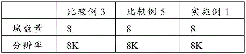

[ Table 3]

As can be seen from table 1 and fig. 13, in comparative example 2, the transmittance was higher (specifically, improved by 26%) than in comparative example 1. This is because the total area of the dark lines is reduced due to the 1-column arrangement of the liquid crystal domains for the reasons already described.
As can be seen from table 2 and fig. 14, the transmittances of comparative examples 3 and 5 are almost the same. In contrast, the transmittance of example 1 was higher than those of comparative examples 3 and 5. Specifically, in example 2, the transmittance was improved by 23% as compared with comparative examples 3 and 5.
As is clear from table 3 and fig. 15, in comparative example 6, the transmittance was slightly improved (specifically, improved by 4%) as compared with comparative example 4. In contrast, in example 2, the transmittance was slightly improved (specifically, improved by 12% as compared with comparative example 4) as compared with comparative examples 4 and 6.
As described above, the transmittance is hardly improved by only the 1-column arrangement, and the transmittance can be greatly improved by adopting the configuration of the embodiment of the present invention. As is clear from comparison between tables 2 and 3, the effect of the embodiment of the present invention is more remarkable as the pixel size is smaller (the resolution is higher).
[ other embodiments ]
The configuration of the liquid crystal domain in each of the first subpixel Sp1 and the second subpixel Sp2 is not limited to the example shown in fig. 10. In the example shown in fig. 10, the liquid crystal domains a (the direction of the reference alignment direction is approximately 225 °), B (the direction of the reference alignment direction is approximately 135 °), C (the direction of the reference alignment direction is approximately 315 °), and D (the direction of the reference alignment direction is approximately 45 °) are arranged in this order along the pixel longitudinal direction D1.
In contrast, the arrangement shown in fig. 16 may be adopted. In the example shown in fig. 16, in each of the first subpixel Sp1 and the second subpixel Sp2, the liquid crystal domains C, D, A and B are arranged in this order from the upper side toward the lower side (i.e., along the pixel length direction D1). Even if the arrangement as in the example shown in fig. 16 is employed, the same effect as that in the case of employing the arrangement of fig. 10 can be obtained.
In addition, in the example shown in fig. 10, the boundary of the first subpixel Sp1 and the second subpixel Sp2 is substantially non-parallel to any one of the first slit 11a1, the second slit 11a2, the third slit 11a3, and the fourth slit 11a4, on the basis of the first portion bd1, the second portion bd2, the third portion bd3, and the fourth portion bd4, and further includes a fifth portion bd 5. The fifth portion bd5 may be omitted. However, if the boundary between the first subpixel Sp1 and the second subpixel Sp2 is constituted only by the first portion bd1, the second portion bd2, the third portion bd3, and the fourth portion bd4, it is difficult to make the areas of the four liquid crystal domains substantially equal within each subpixel. Therefore, from the viewpoint of the angle of field characteristic, the boundary between the first subpixel Sp1 and the second subpixel Sp2 preferably includes a portion that is substantially non-parallel to any of the first slit 11a1, the second slit 11a2, the third slit 11a3, and the fourth slit 11a 4.
The liquid crystal display device according to the embodiment of the invention is suitable for applications requiring display of high-quality displays such as television receivers. Embodiments of the present invention are particularly suitable for a liquid crystal display device having high resolution (for example, resolution of 4K or more).
Claims (5)
1. A liquid crystal display device having a plurality of pixels, the liquid crystal display device comprising a first substrate and a second substrate facing each other, and a vertical alignment type liquid crystal layer provided between the first substrate and the second substrate,
the first substrate has a pixel electrode provided in each of the plurality of pixels and a first alignment film provided between the pixel electrode and the liquid crystal layer,
the second substrate has a counter electrode facing the pixel electrode and a second alignment film provided between the counter electrode and the liquid crystal layer,
each of the plurality of pixels includes a first sub-pixel and a second sub-pixel, the first sub-pixel and the second sub-pixel applying mutually different voltages to the liquid crystal layer,
the pixel electrode includes a first sub-pixel electrode disposed in the first sub-pixel and a second sub-pixel electrode disposed in the second sub-pixel,
each of the first and second sub-pixels has a first liquid crystal domain, a second liquid crystal domain, a third liquid crystal domain, and a fourth liquid crystal domain whose reference alignment directions defined by the first and second alignment films are different from each other,
each of the plurality of pixels has a long side direction and a short side direction referred to as a pixel long side direction and a pixel short side direction, respectively, and the reference alignment directions of the first, second, third, and fourth liquid crystal domains are referred to as first, second, third, and fourth directions, respectively, the first, second, third, and fourth directions form an angle substantially equal to an odd multiple of 45 DEG with respect to the pixel short side direction,
each of the first and second subpixel electrodes has a first slit formed in a region corresponding to the first liquid crystal domain and extending substantially parallel to the first direction, a second slit formed in a region corresponding to the second liquid crystal domain and extending substantially parallel to the second direction, a third slit formed in a region corresponding to the third liquid crystal domain and extending substantially parallel to the third direction, and a fourth slit formed in a region corresponding to the fourth liquid crystal domain and extending substantially parallel to the fourth direction,
in each of the first and second sub-pixels, the first, second, third, and fourth liquid crystal domains are sequentially aligned along a long side direction of the pixel,
the first sub-pixel and the second sub-pixel are adjacent to each other in the pixel short side direction,
the boundary of the first sub-pixel and the second sub-pixel includes a portion substantially parallel to the first slit, a portion substantially parallel to the second slit, a portion substantially parallel to the third slit, and a portion substantially parallel to the fourth slit.
2. The liquid crystal display device according to claim 1, wherein when an azimuth angle of a pixel short side direction is 0 °, the first direction, the second direction, the third direction, and the fourth direction are substantially 225 ° direction, substantially 135 ° direction, substantially 315 ° direction, and substantially 45 ° direction, respectively.
3. The liquid crystal display device according to claim 1, wherein when an azimuth angle of a pixel short side direction is 0 °, the first direction, the second direction, the third direction, and the fourth direction are substantially 315 ° direction, substantially 45 ° direction, substantially 225 ° direction, and substantially 135 ° direction, respectively.
4. The liquid crystal display device according to any one of claims 1 to 3, wherein each of the first alignment film and the second alignment film is a photo-alignment film.
5. The liquid crystal display device according to any one of claims 1 to 3, wherein a pretilt direction defined by the first alignment film and a pretilt direction defined by the second alignment film are substantially antiparallel to each of the first liquid crystal domain, the second liquid crystal domain, the third liquid crystal domain, and the fourth liquid crystal domain.
Applications Claiming Priority (2)
| Application Number | Priority Date | Filing Date | Title |
|---|---|---|---|
| US201962853982P | 2019-05-29 | 2019-05-29 | |
| US62/853982 | 2019-05-29 |
Publications (2)
| Publication Number | Publication Date |
|---|---|
| CN112015012A true CN112015012A (en) | 2020-12-01 |
| CN112015012B CN112015012B (en) | 2023-02-28 |
Family
ID=73506837
Family Applications (1)
| Application Number | Title | Priority Date | Filing Date |
|---|---|---|---|
| CN202010469569.8A Active CN112015012B (en) | 2019-05-29 | 2020-05-28 | Liquid crystal display device having a plurality of pixel electrodes |
Country Status (2)
| Country | Link |
|---|---|
| US (1) | US11079633B2 (en) |
| CN (1) | CN112015012B (en) |
Cited By (1)
| Publication number | Priority date | Publication date | Assignee | Title |
|---|---|---|---|---|
| WO2023123294A1 (en) * | 2021-12-30 | 2023-07-06 | 京东方科技集团股份有限公司 | Liquid crystal display panel and manufacturing method therefor, and display apparatus |
Citations (7)
| Publication number | Priority date | Publication date | Assignee | Title |
|---|---|---|---|---|
| US20070222931A1 (en) * | 2006-03-24 | 2007-09-27 | Quanta Display Inc. | Liquid crystal display |
| JP2008145700A (en) * | 2006-12-08 | 2008-06-26 | Sharp Corp | Liquid crystal display device and manufacturing method thereof |
| CN102395920A (en) * | 2009-04-17 | 2012-03-28 | 夏普株式会社 | Liquid crystal display device |
| US20120154727A1 (en) * | 2010-12-15 | 2012-06-21 | Haksun Chang | Liquid crystal display panel |
| CN103439838A (en) * | 2013-04-12 | 2013-12-11 | 友达光电股份有限公司 | Pixel structure |
| CN105988241A (en) * | 2015-03-18 | 2016-10-05 | 三星显示有限公司 | Curved display device |
| CN108027536A (en) * | 2015-09-17 | 2018-05-11 | 夏普株式会社 | Liquid crystal display panel |
Family Cites Families (6)
| Publication number | Priority date | Publication date | Assignee | Title |
|---|---|---|---|---|
| JP4342200B2 (en) | 2002-06-06 | 2009-10-14 | シャープ株式会社 | Liquid crystal display |
| JP4248306B2 (en) | 2002-06-17 | 2009-04-02 | シャープ株式会社 | Liquid crystal display |
| US7995177B2 (en) | 2005-06-09 | 2011-08-09 | Sharp Kabushiki Kaisha | Liquid crystal display device |
| US10712596B2 (en) * | 2013-08-02 | 2020-07-14 | Samsung Display Co., Ltd. | Liquid crystal display |
| CN108139631B (en) | 2015-10-02 | 2021-06-11 | 夏普株式会社 | Liquid crystal display panel, and method and apparatus for manufacturing the same |
| KR102459604B1 (en) * | 2016-01-06 | 2022-10-31 | 삼성디스플레이 주식회사 | Display substrate and liquid crystal display comprising the same |
-
2020
- 2020-05-28 US US16/885,944 patent/US11079633B2/en active Active
- 2020-05-28 CN CN202010469569.8A patent/CN112015012B/en active Active
Patent Citations (7)
| Publication number | Priority date | Publication date | Assignee | Title |
|---|---|---|---|---|
| US20070222931A1 (en) * | 2006-03-24 | 2007-09-27 | Quanta Display Inc. | Liquid crystal display |
| JP2008145700A (en) * | 2006-12-08 | 2008-06-26 | Sharp Corp | Liquid crystal display device and manufacturing method thereof |
| CN102395920A (en) * | 2009-04-17 | 2012-03-28 | 夏普株式会社 | Liquid crystal display device |
| US20120154727A1 (en) * | 2010-12-15 | 2012-06-21 | Haksun Chang | Liquid crystal display panel |
| CN103439838A (en) * | 2013-04-12 | 2013-12-11 | 友达光电股份有限公司 | Pixel structure |
| CN105988241A (en) * | 2015-03-18 | 2016-10-05 | 三星显示有限公司 | Curved display device |
| CN108027536A (en) * | 2015-09-17 | 2018-05-11 | 夏普株式会社 | Liquid crystal display panel |
Cited By (2)
| Publication number | Priority date | Publication date | Assignee | Title |
|---|---|---|---|---|
| WO2023123294A1 (en) * | 2021-12-30 | 2023-07-06 | 京东方科技集团股份有限公司 | Liquid crystal display panel and manufacturing method therefor, and display apparatus |
| US12235547B2 (en) | 2021-12-30 | 2025-02-25 | Chengdu Boe Display Sci-Tech Co., Ltd. | Liquid crystal display panel and method for manufacturing same, and display device |
Also Published As
| Publication number | Publication date |
|---|---|
| US20200379303A1 (en) | 2020-12-03 |
| CN112015012B (en) | 2023-02-28 |
| US11079633B2 (en) | 2021-08-03 |
Similar Documents
| Publication | Publication Date | Title |
|---|---|---|
| US10838267B2 (en) | Liquid crystal display comprising a pixel electrode having a transverse stem, a longitudinal stem, and a plurality of minute branches | |
| JP6240432B2 (en) | Liquid crystal display | |
| US7518684B2 (en) | Pixel structure and liquid crystal display panel | |
| US8836900B2 (en) | Array substrate and liquid crystal display device | |
| RU2510065C2 (en) | Liquid crystal display device | |
| US20140210868A1 (en) | Liquid crystal display device and method of driving the same | |
| JP2014048652A (en) | Liquid crystal display device | |
| KR20100055154A (en) | Liquid crystal display and driving method thereof | |
| US9465263B2 (en) | Liquid crystal display device having an overlapping pixel electrode and data line | |
| US20100045915A1 (en) | Liquid crystal display | |
| CN110446971B (en) | Liquid crystal display device having a plurality of pixel electrodes | |
| JP6433201B2 (en) | Liquid crystal display | |
| US20070235735A1 (en) | Liquid crystal display | |
| US8094250B2 (en) | Wide viewing angle liquid crystal display with high response speed | |
| US20090316102A1 (en) | Liquid crystal display | |
| US8134670B2 (en) | Liquid crystal display and panel thereof | |
| CN112015012B (en) | Liquid crystal display device having a plurality of pixel electrodes | |
| KR101156510B1 (en) | In-plain switching liquid crystal display device | |
| CN112015011B (en) | Liquid crystal display device having a light shielding layer | |
| CN111694192B (en) | Liquid crystal display device having a light shielding layer | |
| US12105389B1 (en) | Display panel | |
| JP2023116374A (en) | Liquid crystal display device | |
| KR20060083096A (en) | Thin film transistor array panel | |
| KR20120044777A (en) | Liquid crsytal display |
Legal Events
| Date | Code | Title | Description |
|---|---|---|---|
| PB01 | Publication | ||
| PB01 | Publication | ||
| SE01 | Entry into force of request for substantive examination | ||
| SE01 | Entry into force of request for substantive examination | ||
| GR01 | Patent grant | ||
| GR01 | Patent grant |