CN111987909A - Interleaved parallel DC/DC converter and control method thereof - Google Patents
Interleaved parallel DC/DC converter and control method thereof Download PDFInfo
- Publication number
- CN111987909A CN111987909A CN202010778777.6A CN202010778777A CN111987909A CN 111987909 A CN111987909 A CN 111987909A CN 202010778777 A CN202010778777 A CN 202010778777A CN 111987909 A CN111987909 A CN 111987909A
- Authority
- CN
- China
- Prior art keywords
- diode
- inductor
- output
- current
- voltage
- Prior art date
- Legal status (The legal status is an assumption and is not a legal conclusion. Google has not performed a legal analysis and makes no representation as to the accuracy of the status listed.)
- Pending
Links
Images


Classifications
-
- H—ELECTRICITY
- H02—GENERATION; CONVERSION OR DISTRIBUTION OF ELECTRIC POWER
- H02M—APPARATUS FOR CONVERSION BETWEEN AC AND AC, BETWEEN AC AND DC, OR BETWEEN DC AND DC, AND FOR USE WITH MAINS OR SIMILAR POWER SUPPLY SYSTEMS; CONVERSION OF DC OR AC INPUT POWER INTO SURGE OUTPUT POWER; CONTROL OR REGULATION THEREOF
- H02M3/00—Conversion of DC power input into DC power output
- H02M3/02—Conversion of DC power input into DC power output without intermediate conversion into AC
- H02M3/04—Conversion of DC power input into DC power output without intermediate conversion into AC by static converters
- H02M3/10—Conversion of DC power input into DC power output without intermediate conversion into AC by static converters using discharge tubes with control electrode or semiconductor devices with control electrode
- H02M3/145—Conversion of DC power input into DC power output without intermediate conversion into AC by static converters using discharge tubes with control electrode or semiconductor devices with control electrode using devices of a triode or transistor type requiring continuous application of a control signal
- H02M3/155—Conversion of DC power input into DC power output without intermediate conversion into AC by static converters using discharge tubes with control electrode or semiconductor devices with control electrode using devices of a triode or transistor type requiring continuous application of a control signal using semiconductor devices only
- H02M3/156—Conversion of DC power input into DC power output without intermediate conversion into AC by static converters using discharge tubes with control electrode or semiconductor devices with control electrode using devices of a triode or transistor type requiring continuous application of a control signal using semiconductor devices only with automatic control of output voltage or current, e.g. switching regulators
- H02M3/158—Conversion of DC power input into DC power output without intermediate conversion into AC by static converters using discharge tubes with control electrode or semiconductor devices with control electrode using devices of a triode or transistor type requiring continuous application of a control signal using semiconductor devices only with automatic control of output voltage or current, e.g. switching regulators including plural semiconductor devices as final control devices for a single load
Landscapes
- Engineering & Computer Science (AREA)
- Power Engineering (AREA)
- Dc-Dc Converters (AREA)
Abstract
本发明公开了一种交错并联DC/DC变换器及控制方法,其中变换器包括开关电感单元、升压单元、输出电路,所述开关电感单元的输入端连接电压源,其输出端连接升压单元,所述升压单元的输出端连接输出电路,经输出电路引出输出端,所述输出端输出升压后的电压信号。本发明的优点在于:整个电路结构对称简单,控制方便,输出电压增益更高。

The invention discloses an interleaved parallel DC/DC converter and a control method, wherein the converter includes a switched inductance unit, a boosting unit, and an output circuit. The output terminal of the boosting unit is connected to the output circuit, and the output terminal is led out through the output circuit, and the output terminal outputs the boosted voltage signal. The advantages of the invention are: the whole circuit structure is symmetrical and simple, the control is convenient, and the output voltage gain is higher.
Description
技术领域technical field
本发明涉及电力电子技术领域,特别涉及一种交错并联DC/DC变换器及其控制方法。The invention relates to the technical field of power electronics, in particular to an interleaved parallel DC/DC converter and a control method thereof.
背景技术Background technique
随着化石能源的日益枯竭与其燃烧后对环境的污染问题等越来越受到国际社会的关注之后。寻找新型、可再生、无污染的能源成为了摆在人类面前迫在眉睫的大事。光伏电能因其取之不尽用之不竭、清洁无污染等优点,成为了人们对未来能源需求研究的重点课题,潜力巨大。With the increasing depletion of fossil energy and the pollution of the environment after burning, it has attracted more and more attention from the international community. The search for new, renewable and non-polluting energy has become an urgent task for mankind. Photovoltaic power has become a key topic in people's research on future energy demand due to its inexhaustible, clean and pollution-free advantages, with huge potential.
由于光伏发电系统中光伏板直接输出的直流电压较低,一般为30-50V,而针对AC220V的市电,即使是使用全桥并网逆变器,其直流输入母线电压一般也要380V,如何实现高增益DC-DC升压是实现光伏并网发电系统中急需要解决的问题之一。Since the direct output DC voltage of the photovoltaic panels in the photovoltaic power generation system is low, generally 30-50V, and for the AC220V mains, even if a full-bridge grid-connected inverter is used, the DC input bus voltage is generally 380V. Achieving high-gain DC-DC boost is one of the urgent problems to be solved in the realization of photovoltaic grid-connected power generation systems.
虽然Boost变换器当占空比接近1时,在理论上其电压增益可以接近无穷大,但随着开关关断时间的缩短:其电感电流纹波,功率器件峰值电流和输出电流纹波都将逐渐变大;其有源开关管和无源开关管的电压应力等于输出电压,过大的电压应力会大大增加变换器的功率损耗降低变换器的传输效率。Although the voltage gain of the boost converter can be theoretically close to infinity when the duty cycle is close to 1, with the shortening of the switch off time: its inductor current ripple, power device peak current and output current ripple will gradually increase The voltage stress of the active switch tube and the passive switch tube is equal to the output voltage. Excessive voltage stress will greatly increase the power loss of the converter and reduce the transmission efficiency of the converter.
由于光伏板受到环境的影响,输出电压不稳定有波动,从而经过变换器的升压后,变换器输出电压不稳定有波动,故而需要设计一种新的交错并联DC/DC变换器及其控制方法。Because the photovoltaic panel is affected by the environment, the output voltage is unstable and fluctuates, so after the boost of the converter, the output voltage of the converter is unstable and fluctuates, so it is necessary to design a new interleaved parallel DC/DC converter and its control method.
发明内容SUMMARY OF THE INVENTION
本发明的目的在于克服现有技术的不足,提供一种交错并联DC/DC变换器,用于实现变换器输出电压增益更高,且可以满足提升电压输出的稳定性。The purpose of the present invention is to overcome the deficiencies of the prior art, and to provide an interleaved parallel DC/DC converter, which is used to achieve higher output voltage gain of the converter and can satisfy the stability of the improved voltage output.
为了实现上述目的,本发明采用的技术方案为:一种交错并联DC/DC变换器,包括开关电感单元、升压单元、输出电路,所述开关电感单元的输入端连接电压源,其输出端连接升压单元,所述升压单元的输出端连接输出电路,经输出电路引出输出端,所述输出端输出升压后的电压信号。In order to achieve the above purpose, the technical solution adopted in the present invention is as follows: an interleaved parallel DC/DC converter, comprising a switched inductance unit, a boosting unit and an output circuit, the input end of the switched inductance unit is connected to a voltage source, and the output end of the switched inductance unit is connected to a voltage source. A boosting unit is connected, an output end of the boosting unit is connected to an output circuit, an output end is led out through the output circuit, and the output end outputs a boosted voltage signal.
所述升压单元接收控制信号并根据控制信号输出对应的电压。The boosting unit receives the control signal and outputs a corresponding voltage according to the control signal.
所述开关电感单元包括第一开关电感单元、第二开关电感单元,所述第一开关电感单元、第二开关电感单元用于存储电压源的电能或将存储的电能进行放电。The switched inductor unit includes a first switched inductor unit and a second switched inductor unit, and the first switched inductor unit and the second switched inductor unit are used for storing the electrical energy of the voltage source or discharging the stored electrical energy.
所述第一开关电感单元包括第一电感L1、第二电感L2、第一二极管D1、第二二极管D2和第五二极管D5;The first switched inductor unit includes a first inductor L 1 , a second inductor L 2 , a first diode D 1 , a second diode D 2 and a fifth diode D5;
所述第二开关电感单元包括第三电感L3、第四电感L4、第三二极管D3、第四二极管D4和第六二极管D6;The second switched inductor unit includes a third inductor L 3 , a fourth inductor L 4 , a third diode D 3 , a fourth diode D 4 and a sixth diode D 6 ;
电压源的输出正极分别连接至第一电感L1的一端、第一二极管D1的阳极、第三二极管D3的阳极以及第三电感L3的一端,第一电感L3的另一端分别连接第二二极管D2的阳极、第五二极管D5的阳极,第五二极管D5的阴极分别连接第一二极管D1的阴极、第二电感L2的一端,第二电感L2的另一端连接第二二极管D2的阴极,第二二极管D2的阴极引出第一开关电感单元的输出端子K1;The output anode of the voltage source is respectively connected to one end of the first inductor L1, the anode of the first diode D1, the anode of the third diode D3, and one end of the third inductor L3, and the other end of the first inductor L3 is connected to the first inductor L3 respectively. The anode of the second diode D2, the anode of the fifth diode D5, and the cathode of the fifth diode D5 are respectively connected to the cathode of the first diode D1, one end of the second inductor L2, and the other end of the second inductor L2 The cathode of the second diode D2 is connected, and the cathode of the second diode D2 leads to the output terminal K1 of the first switched inductance unit;
第三电感L3的另一端分别连接第四二极管D4的阳极、第六二极管D6的阳极,第六二极管D6的阴极分别连接第三二极管D3的阴极以及第四电感L4的一端,第四电感L4的另一端连接第四二极管D4的阴极,第四二极管D4的阴极引出第二开关电感单元的输出端子K2;The other end of the third inductor L3 is connected to the anode of the fourth diode D4 and the anode of the sixth diode D6 respectively, and the cathode of the sixth diode D6 is respectively connected to the cathode of the third diode D3 and the fourth inductor L4 one end of the fourth inductance L4, the other end of the fourth inductance L4 is connected to the cathode of the fourth diode D4, and the cathode of the fourth diode D4 leads to the output terminal K2 of the second switched inductance unit;
输出端子K1、K2用于分别连接至升压单元的输入端。The output terminals K1 and K2 are used to connect to the input terminals of the boosting unit respectively.
所述升压单元包括MOS管S1、S2、第一电容C1、第二电容C2、第三电容C3、第七二极管D7、第八二极管D8、第九二极管D9;The boosting unit includes MOS transistors S1, S2, a first capacitor C1, a second capacitor C2, a third capacitor C3, a seventh diode D7, an eighth diode D8, and a ninth diode D9;
所述MOS管S1的栅极、MOS管S2的栅极分别输入控制信号,用于控制MOS管S1、S2的导通;The gate of the MOS transistor S1 and the gate of the MOS transistor S2 are respectively input with control signals for controlling the conduction of the MOS transistors S1 and S2;
输出端子K1分别连接至MOS管S2的源极以及第一电容C1的一端,第一电容C1的另一端分别连接第九二极管D9的阴极、第二电容C2的一端,第二电容C2的另一端分别连接第七二极管D7的阴极以及第八二极管D8的阳极;输出端子K2分别连接MOS管S1的源极以及第七二极管D7的阳极,第三电容C3的一端连接第七二极管D7的阳极,另一端连接第八二极管D8的阴极,D8的阴极连接D9的阳极;The output terminal K1 is respectively connected to the source of the MOS transistor S2 and one end of the first capacitor C1, and the other end of the first capacitor C1 is respectively connected to the cathode of the ninth diode D9 and one end of the second capacitor C2. The other end is respectively connected to the cathode of the seventh diode D7 and the anode of the eighth diode D8; the output terminal K2 is respectively connected to the source of the MOS transistor S1 and the anode of the seventh diode D7, and one end of the third capacitor C3 is connected to The anode of the seventh diode D7, the other end is connected to the cathode of the eighth diode D8, and the cathode of D8 is connected to the anode of D9;
所述MOS管S1的漏极、S2的漏极接电源地;The drain of the MOS transistor S1 and the drain of S2 are connected to the power ground;
所述第九二极管D9的阴极引出升压单元的输出端子。The cathode of the ninth diode D9 leads to the output terminal of the boosting unit.
所述输出电路包括输出二极管D0以及输出电容C0,升压单元您的输出端子连接至输出二极管D0的阳极,D0的阴极经过电容C0接地;在D0的阴极和电容C0之间引出端子作为DC/DC变换器的正极输出端子;在输出电容C0和电源地之间引出端子作为DC/DC变换器的负极输出端子。The output circuit includes an output diode D0 and an output capacitor C0. The output terminal of the boost unit is connected to the anode of the output diode D0, and the cathode of D0 is grounded through the capacitor C0; the terminal between the cathode of D0 and the capacitor C0 is used as DC/ The positive output terminal of the DC converter; the terminal drawn between the output capacitor C0 and the power ground is used as the negative output terminal of the DC/DC converter.
控制占空比PWM信号来分别控制MOS管S1、S2的导通,从而控制变换器的输出电压。The duty cycle PWM signal is controlled to control the conduction of the MOS transistors S1 and S2 respectively, thereby controlling the output voltage of the converter.
一种交错并联DC/DC变换器的控制方法,采用由外部电压环和内部电流环构成的双闭环控制结构对DC/DC变换器的输出电压进行控制。A control method for interleaved parallel DC/DC converters, which adopts a double closed-loop control structure composed of an outer voltage loop and an inner current loop to control the output voltage of the DC/DC converters.
所述控制方法包括:电压外环控制以及电流内环控制,电压外环控制包括将采集的变换器的输出电压V0与设置的理想的参考电压值Vr进行比较得到两者之间的误差值Vw,将Vw送入到PI调节器中进行调节输出达到所需电压对应的电流ir,所述电流ir作为电流内环的参考电流;The control method includes: voltage outer loop control and current inner loop control. The voltage outer loop control includes comparing the collected output voltage V0 of the converter with the set ideal reference voltage value Vr to obtain an error value Vw between the two. , send Vw into the PI regulator to adjust the output to reach the current ir corresponding to the required voltage, and the current ir is used as the reference current of the current inner loop;
电流内环控制包括对应第一开关电感单元的第一电流内环、以及对应第二开关电感单元的第二电流内环;参考电流的二分之一分别作为第一电流内环、第二电流内环的电流给定值,分别与各自的开关电感单元的电流采样值进行比较,得到电流偏差值分别送入到各自对应的电流PI调节器中输出对应的占空比d;The current inner loop control includes a first current inner loop corresponding to the first switched inductance unit and a second current inner loop corresponding to the second switched inductance unit; half of the reference current is used as the first current inner loop and the second current inner loop respectively. The current given value of the inner loop is compared with the current sampling value of the respective switching inductance unit respectively, and the current deviation value is obtained, which is respectively sent to the corresponding current PI regulator to output the corresponding duty cycle d;
所得开关占空比d通过PWM控制环节GPWM(s)实现对开关器件的控制,使得开关占空比d通过从Gid(s)调节器输出各相的电感单元电流;两相开关电感单元电流之和通过变换器电感总电流到输出电压调节器Gvi(s),得出输出电压V0,从而实现双闭环控制。The obtained switching duty cycle d is controlled by the PWM control link G PWM (s) to realize the control of the switching device, so that the switching duty cycle d outputs the inductor unit current of each phase from the G id (s) regulator; the two-phase switch inductor unit The sum of the current passes through the total current of the converter inductor to the output voltage regulator G vi (s), and the output voltage V0 is obtained, thereby realizing double closed-loop control.
本发明的优点在于:整个电路结构对称简单,控制方便,输出电压增益更高;本发明电路利用开关电感单元中电感的并行充电串联放电的特性以及电容与二极管了构成了电容串并联结构,电感的并行充电串联放电、电容的有效充放电,从而升高了输出电压,通过电压外环电流内环双闭环控制,实现了高电压交错并联DC-DC变换器输出电压增益的提升以及稳定的输出。The advantages of the invention are: the whole circuit structure is symmetrical and simple, the control is convenient, and the output voltage gain is higher; the circuit of the invention utilizes the parallel charging and series discharging characteristics of the inductor in the switching inductor unit, and the capacitor and the diode form a capacitor series-parallel structure. The parallel charging and series discharging and the effective charging and discharging of the capacitor increase the output voltage. Through the double closed-loop control of the voltage outer loop and the current inner loop, the improvement of the output voltage gain of the high-voltage interleaved parallel DC-DC converter and the stable output are realized. .
附图说明Description of drawings
下面对本发明说明书各幅附图表达的内容及图中的标记作简要说明:Below is a brief description of the content expressed in each of the drawings in the description of the present invention and the labels in the drawings:
图1是本发明中高增益交错并联DC-DC变换器的结构示意图;1 is a schematic structural diagram of a high-gain interleaved parallel DC-DC converter in the present invention;
图2(a)~(d)是高增益交错并联DC-DC变换器各个不同导通状态下的等效电路图;Figures 2(a)-(d) are the equivalent circuit diagrams of the high-gain interleaved parallel DC-DC converters in different conduction states;
图3是开关器件S1、S2一个周期导通时态图;FIG. 3 is a timing diagram of switching devices S 1 and S 2 being turned on in one cycle;
图4是所提变换器与传统的交错并联变换器输出电压仿真实验波形图;Fig. 4 is the simulation experiment waveform diagram of the output voltage of the proposed converter and the traditional interleaved parallel converter;
图5是交错并联变换器双闭环控制框图;Fig. 5 is the double closed-loop control block diagram of the interleaved parallel converter;
具体实施方式Detailed ways
下面对照附图,通过对最优实施例的描述,对本发明的具体实施方式作进一步详细的说明。The specific embodiments of the present invention will be described in further detail below with reference to the accompanying drawings and through the description of the preferred embodiments.
交错并联DC-DC变换器,该变换器拓扑单元包括:开关电感单元、升压单元、输出二极管D0、输出电容C0 An interleaved parallel DC-DC converter, the converter topology unit includes: a switched inductor unit, a boost unit, an output diode D 0 , and an output capacitor C 0
由第一电感L1、第二电感L2、第一二极管D1、第二二极管D2和第五二极管D5组成第一开关电感单元;由第三电感L3、第四电感L4、第三二极管D3、第四二极管D4和第六二极管D6组成第二开关电感单元;负载R与本申请的变换器连接示意图如图1所示。The first switched inductor unit is composed of the first inductor L 1 , the second inductor L 2 , the first diode D 1 , the second diode D 2 and the fifth diode D 5 ; the third inductor L 3 , The fourth inductor L 4 , the third diode D 3 , the fourth diode D 4 and the sixth diode D 6 form a second switched inductor unit; the schematic diagram of the connection between the load R and the converter of the present application is shown in FIG. 1 Show.
本发明的交错并联DC-DC变换器控制方法采用的技术方案是:采用由外部电压环和内部电流环构成的双闭环控制结构对其电压进行控制,且内部电流环采用电流反馈控制方式或电流复合控制方式,电流反馈控制输出与电流前馈控制输出之和为内部电流环的控制输出;The technical scheme adopted by the control method of the interleaved parallel DC-DC converter of the present invention is as follows: a double closed-loop control structure composed of an outer voltage loop and an inner current loop is used to control its voltage, and the inner current loop adopts a current feedback control method or a current loop. In the composite control mode, the sum of the current feedback control output and the current feedforward control output is the control output of the internal current loop;
所述采用由外部电压环和内部电流环构成的双闭环控制结构对其输出电压进行控制,是通过将变换器的输出电压控制在其期望电压,即通过控制两个功率开关器件的占空比实现的。The double closed-loop control structure consisting of an outer voltage loop and an inner current loop is used to control its output voltage by controlling the output voltage of the converter at its desired voltage, that is, by controlling the duty cycle of the two power switching devices. realized.
如图1所示,一种高增益交错并联DC-DC变换器,包括电压源、两个开关电感单元、第一MOS管S1、第二MOS管S2、第一电容C1、升压单元、输出二极管D0、输出电容C0、负载R构成变换器电路。As shown in FIG. 1 , a high-gain interleaved parallel DC-DC converter includes a voltage source, two switched inductor units, a first MOS transistor S 1 , a second MOS transistor S 2 , a first capacitor C 1 , a booster The unit, the output diode D 0 , the output capacitor C 0 , and the load R constitute a converter circuit.
电路的具体连接方式为:The specific connection method of the circuit is as follows:
所述电压源Uin的正极分别与第一电感L1、第一二极管D1的阳极、第三电感L3的一端和第四二极管D4的阳极连接;第一电感L1分别与第二二极管D2和第五二极管D5的阳极连接;第一二极管D1的阴极分别与第五二极管D5的阴极和第二电感L2的一端连接;第二二极管D2的阴极分别与第二电感L2的另一端、第一电容C1的阳极和第二MOS管S2源极连接;第三二极管D3的阴极分别与第六二极管D6的阴极和第四电感L4的一端连接;第四二极管D4的阴极分别与第四电感L4的另一端、第一MOS管S1的源极、第七二极管D7的阳极和第三电容C3的阳极连接;第一电容C1的阴极分别与第二电容C2的阴极、第九二极管D9的阴极和输出二极管D0的阳极连接;第八二极管D8阳极分别与第二电容C2的阳极和第七二极管D7的阴极连接;第八二极管D8的阴极分别与第九二极管D9的阳极和第三电容C3的阴极连接;输出二极管D0的阴极分别与输出电容C0的阳极和负载R的一端连接;电压源Uin的负极分别与第一MOS管S1的漏极、第二MOS管S2的漏极、输出电容C0的阴极和负载(R)的另一端连接。负载R作为变换器的输出电压的直接负载,可以为现有技术不同的应用负载。The anode of the voltage source U in is respectively connected to the first inductor L 1 , the anode of the first diode D 1 , one end of the third inductor L 3 and the anode of the fourth diode D 4 ; the first inductor L 1 are respectively connected with the anodes of the second diode D2 and the fifth diode D5; the cathodes of the first diode D1 are respectively connected with the cathodes of the fifth diode D5 and one end of the second inductor L2 ; The cathode of the second diode D 2 is respectively connected with the other end of the second inductor L 2 , the anode of the first capacitor C 1 and the source of the second MOS tube S 2 ; the cathode of the third diode D 3 is respectively connected with The cathode of the sixth diode D6 is connected to one end of the fourth inductance L4; the cathode of the fourth diode D4 is respectively connected to the other end of the fourth inductance L4, the source of the first MOS transistor S1, the The anode of the seven diodes D7 is connected to the anode of the third capacitor C3; the cathode of the first capacitor C1 is connected to the cathode of the second capacitor C2, the cathode of the ninth diode D9 and the cathode of the output diode D0 respectively. The anode is connected; the anode of the eighth diode D8 is respectively connected with the anode of the second capacitor C2 and the cathode of the seventh diode D7; the cathode of the eighth diode D8 is respectively connected with the anode of the ninth diode D9 and the cathode of the seventh diode D7; The cathode of the third capacitor C3 is connected; the cathode of the output diode D0 is connected to the anode of the output capacitor C0 and one end of the load R respectively; the cathode of the voltage source Uin is respectively connected to the drain of the first MOS tube S1, the second MOS The drain of the tube S2, the cathode of the output capacitor C0 and the other end of the load (R) are connected. The load R, as a direct load of the output voltage of the converter, can be a load for different applications in the prior art.
第一电容C1、第二电容C2、第三电容C3和输出电容C0均为电解电容。The first capacitor C 1 , the second capacitor C 2 , the third capacitor C 3 and the output capacitor C 0 are all electrolytic capacitors.
如图3所示为一个周期内开关器件S1、S2导通示意图,Ugs1对应S1的栅极电压,当其为高电平则导通;同理Ugs2是S2的栅极电压。结合其导通图分析其工作原理如下:Figure 3 shows a schematic diagram of the conduction of the switching devices S1 and S2 in one cycle. Ugs1 corresponds to the gate voltage of S1, and is turned on when it is at a high level; similarly, Ugs2 is the gate voltage of S2. Combined with its conduction diagram, its working principle is as follows:
本发明的变换器的具体工作过程:The concrete working process of the converter of the present invention:
模态1,如图2(a)所示,MOS管S1关断,S2导通。二极管D3、D4、D5、D8、D0受到反向电压截止。电压源向第一开关电感单元1中的电感L1和电感L2充电储能,电压源与第二开关电感单元2中电感L3和电感L4串联放电。电容C2、C3并联放电给电容C1。负载R由输出电容C0获得能量。拓扑放电回路为Uin-L3-D6-L4-D7-C2-C1-S2与Uin-L3-D6-L4-C2-D9-C1-S2。In mode 1 , as shown in Figure 2 (a), MOS transistor S1 is turned off and S2 is turned on. Diodes D 3 , D 4 , D 5 , D 8 , D 0 are cut off by reverse voltage. The voltage source charges and stores energy to the inductor L 1 and the inductor L 2 in the first switched
模态2,如图2(b)所示,控制信号控制开关器件S1、S2导通。二极管D1、D2、D3、D4正向导通,D5、D7、D8、D9、D0受到反向电压截止关断。电压源向第一开关电感单元1中电感L1和电感L2并联储能,电压源向第二开关电感单元2中电感L3和电感L4并联储能。输出电容C0把存储的能量向负载R释放。In
模态3,如图2(c)所示,控制信号使开关器件S1导通、S2关断。二极管D3、D4、D5、D8正向导通,二极管D1、D2、D6、D7、D9、D0受到反向电压截止关断。输入电压Uin串联开关电感单元1中电感L1和L2,电容C1向电容C2、C3充电。输入电压Uin向开关电感单元2中电感L3和L4并联储能。在该模式下,流过电感L1和L2电流逐渐减小,电容C2和C3两端电压逐渐增大。拓扑放电回路为第一个回路Uin-L1-D5-L2-C1-C2-D8-C3-S1和第二个回路Uin-L3-D4-S1、第三个回路Uin-D3-L4-S1。In
模态4,如图2(d)所示,制信号使开关器件S1导通、S2关断。二极管D3、D4、D5、D8正向导通,二极管D1、D2、D6、D7、D9、D0受到反向电压截止关断。电容C1向电容C2、C3充电。输入电压Uin向开关电感单元2中电感L3和L4并联储能。电容C2和C3串联的两端电压高于输出电容C0电压,二极管D0正向导通。拓扑放电回路为:Uin-L1-D5-L2-C1-D0-C0(R)和Uin-L1-D5-L2-C1-C2-D8-C3-S1。In
在一个开关周期内,令输出电压为U0,当变换器进入稳态工作后,得出以下的电压关系推导过程。In one switching cycle, let the output voltage be U 0 , when the converter enters steady state operation, the following voltage relationship derivation process is obtained.
在模态1和模态2持续时间为D10TS,电感L1和电感L2的电流增加量为:In

D10为开关器件S1的占空比,TS为开关器件S1的开关周期,t0-t2为模态1和模态2的所处的时段D 10 is the duty cycle of the switching device S 1 , T S is the switching period of the switching device S 1 , and t 0 -t 2 is the time period of
在模态3和模态4持续时间为(1-D1)TS,电感L1和L2电流减小量为In
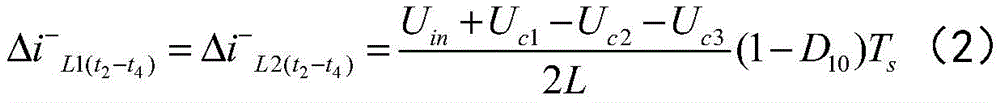
D10为开关器件S1的占空比,TS为开关器件S1的开关周期,t2-t4为模态3和模态4的所处的时段D 10 is the duty cycle of the switching device S 1 , T S is the switching period of the switching device S 1 , and t 2 -t 4 is the period of
模态1持续时间为(1-D20)Ts,电感L3和L4电流减小量为:The

D20为开关器件S1的占空比,TS为开关器件S2的开关周期,t2-t4为模态1所处的时段D 20 is the duty cycle of the switching device S 1 , T S is the switching period of the switching device S 2 , and t 2 -t 4 is the period during which
在模态2、模态3和模态4持续时间为D20Ts,电感L3和L4电流增加量为:In

D20为开关器件S1的占空比,TS为开关器件S2的开关周期,t2-t5为模态2、模态3和模态4所处的时段D 20 is the duty cycle of the switching device S 1 , T S is the switching period of the switching device S 2 , and t 2 -t 5 is the period of
由式(1)-(4),对电感L1和电感L3的伏秒平衡定理,得:From equations (1)-(4), and the volt-second balance theorem for inductance L 1 and inductance L 3 , we get:

根据电路结构的对称性,得:According to the symmetry of the circuit structure, we get:

由(5)-(6),当控制信号控制开关器件占空比D10=D20=D时,本文所提变换器拓扑电压增益为:From (5)-(6), when the control signal controls the switching device duty cycle D 10 =D 20 =D, the voltage gain of the converter topology proposed in this paper is:

由于光伏板的输出电压不稳定,控制目标是将高增益交错并联DC-DC变换器高压侧电压U0保持在理想值Uref。为此,高增益交错并联DC-DC变换器采取如图5所示的电压电流双闭环控制方式,其工作原理如下:Since the output voltage of the photovoltaic panel is unstable, the control objective is to maintain the high-voltage side voltage U 0 of the high-gain interleaved parallel DC-DC converter at the ideal value U ref . To this end, the high-gain interleaved parallel DC-DC converter adopts the voltage and current double closed-loop control method as shown in Figure 5, and its working principle is as follows:
光伏板的输入电压Uin经过变换器转换得到输出电压U0,将其与理想的参考电压信号值Ur进行比较判断两者之间有无差值,即为误差电压Uw,随后将误差电压Uw送进PI调节器调节输出达到所需电压的电流ir。由于变换器采用两相交错并联技术,单相中开关电感单元是给定电流的一半。所得到的电流给定值与各相中的负反馈电感单元电流的的采样值进行比较,所得的电流偏差值经过电流PI调节器调节,输出电路为达到目的电压的开关占空比d。所得开关占空比d通过PWM控制环节GPWM(s)实现对开关器件的控制,使得开关占空比d通过从Gid(s)调节器输出各相的电感单元电流;两相开关电感单元电流之和通过变换器电感总电流到输出电压调节器Gvi(s),得出输出电压v。通过电压电流双闭环控制时,在输入电压波动时输出电压经过调整依然能够保持稳定。其中GPWM(s)为输出的PWM调节器的调制器函数,Ki(s)、Kv(s)为电流环、电压环调节系数;Gvi(s)、Gid(s)为通过状态空间法得到了一个周期的状态空间方程,然后对方程进行S变换,最终得到的占空比d到电感电流传递函数Gid(s)、占空比到输出电压函数Gvi(s)。如图4所示,为通过软件仿真后的本申请变换器相对应现有变换器的波形图,有图也可以看出,本申请具有较高的增益,可以做到输出更大更稳定的电压,同时电路结构简单可靠。The input voltage U in of the photovoltaic panel is converted by the converter to obtain the output voltage U 0 , which is compared with the ideal reference voltage signal value Ur to determine whether there is a difference between the two, which is the error voltage U w , and then the error The voltage U w is fed into the PI regulator to adjust the output current ir to the desired voltage. Since the converter adopts two-phase interleaved parallel technology, the switching inductance unit in single-phase is half of the given current. The obtained current given value is compared with the sampling value of the current of the negative feedback inductor unit in each phase, the obtained current deviation value is adjusted by the current PI regulator, and the output circuit is the switch duty cycle d that achieves the target voltage. The obtained switching duty cycle d is controlled by the PWM control link G PWM (s) to realize the control of the switching device, so that the switching duty cycle d outputs the inductor unit current of each phase from the G id (s) regulator; the two-phase switch inductor unit The sum of the currents passes through the converter inductor total current to the output voltage regulator Gvi (s), resulting in the output voltage v. When the voltage and current double closed-loop control is used, the output voltage can still be stable after adjustment when the input voltage fluctuates. Among them, G PWM (s) is the modulator function of the output PWM regulator, Ki (s) and Kv (s) are the current loop and voltage loop adjustment coefficients; G vi (s) and G id (s) are the passing state space The method obtains a periodic state space equation, and then performs S transformation on the equation, and finally obtains the duty cycle d to the inductor current transfer function G id (s), and the duty cycle to the output voltage function G vi (s). As shown in FIG. 4 , for the waveform diagram of the converter of the present application corresponding to the existing converter after software simulation, it can be seen from the figure that the present application has a higher gain, and can achieve a larger and more stable output. voltage, and the circuit structure is simple and reliable.
显然本发明具体实现并不受上述方式的限制,只要采用了本发明的方法构思和技术方案进行的各种非实质性的改进,均在本发明的保护范围之内。Obviously, the specific implementation of the present invention is not limited by the above-mentioned manner, as long as various insubstantial improvements made by adopting the method concept and technical solution of the present invention are all within the protection scope of the present invention.
Claims (9)
Priority Applications (1)
| Application Number | Priority Date | Filing Date | Title |
|---|---|---|---|
| CN202010778777.6A CN111987909A (en) | 2020-08-05 | 2020-08-05 | Interleaved parallel DC/DC converter and control method thereof |
Applications Claiming Priority (1)
| Application Number | Priority Date | Filing Date | Title |
|---|---|---|---|
| CN202010778777.6A CN111987909A (en) | 2020-08-05 | 2020-08-05 | Interleaved parallel DC/DC converter and control method thereof |
Publications (1)
| Publication Number | Publication Date |
|---|---|
| CN111987909A true CN111987909A (en) | 2020-11-24 |
Family
ID=73445064
Family Applications (1)
| Application Number | Title | Priority Date | Filing Date |
|---|---|---|---|
| CN202010778777.6A Pending CN111987909A (en) | 2020-08-05 | 2020-08-05 | Interleaved parallel DC/DC converter and control method thereof |
Country Status (1)
| Country | Link |
|---|---|
| CN (1) | CN111987909A (en) |
Cited By (1)
| Publication number | Priority date | Publication date | Assignee | Title |
|---|---|---|---|---|
| CN116155102A (en) * | 2023-04-20 | 2023-05-23 | 深圳市恒运昌真空技术有限公司 | High-gain converter |
Citations (4)
| Publication number | Priority date | Publication date | Assignee | Title |
|---|---|---|---|---|
| TW201130211A (en) * | 2010-02-26 | 2011-09-01 | Sheng-Yu Tseng | An interleaving converter |
| CN107317479A (en) * | 2017-06-16 | 2017-11-03 | 辽宁工程技术大学 | A kind of staggered high-gain Boost of magnetic integrated switch inductance |
| CN207269198U (en) * | 2017-07-12 | 2018-04-24 | 燕山大学 | A high-gain dual-input DC converter based on capacitor series-parallel structure |
| CN109462330A (en) * | 2018-11-13 | 2019-03-12 | 天津大学 | The high voltage boosting dc converter of belt switch inductance and switching capacity |
-
2020
- 2020-08-05 CN CN202010778777.6A patent/CN111987909A/en active Pending
Patent Citations (4)
| Publication number | Priority date | Publication date | Assignee | Title |
|---|---|---|---|---|
| TW201130211A (en) * | 2010-02-26 | 2011-09-01 | Sheng-Yu Tseng | An interleaving converter |
| CN107317479A (en) * | 2017-06-16 | 2017-11-03 | 辽宁工程技术大学 | A kind of staggered high-gain Boost of magnetic integrated switch inductance |
| CN207269198U (en) * | 2017-07-12 | 2018-04-24 | 燕山大学 | A high-gain dual-input DC converter based on capacitor series-parallel structure |
| CN109462330A (en) * | 2018-11-13 | 2019-03-12 | 天津大学 | The high voltage boosting dc converter of belt switch inductance and switching capacity |
Non-Patent Citations (1)
| Title |
|---|
| 马红伟: ""基于储能的直流微电网双向DC/DC变换器的优化设计"", 《中国优秀硕士学位论文全文数据库 工程科技II辑》 * |
Cited By (1)
| Publication number | Priority date | Publication date | Assignee | Title |
|---|---|---|---|---|
| CN116155102A (en) * | 2023-04-20 | 2023-05-23 | 深圳市恒运昌真空技术有限公司 | High-gain converter |
Similar Documents
| Publication | Publication Date | Title |
|---|---|---|
| CN109980978B (en) | A converter and its modulation method | |
| CN104868725B (en) | A kind of non-isolated three-port DC converter of booster type and its control method | |
| CN107834886B (en) | A kind of single-stage boost inverter and its control method | |
| CN110957922B (en) | Single-stage high-frequency isolated bidirectional DC converter and grid-connected energy storage system | |
| CN105939112B (en) | A kind of quasi- boost switching DC-DC converter of high-gain | |
| CN110912245B (en) | Three-port integrated photovoltaic energy storage converter | |
| CN105939107B (en) | Mixed quasi-switch boosting DC-DC converter | |
| CN113541500A (en) | Isolated semi-accurate Z source direct current boost converter | |
| CN106712523A (en) | Boost three-level full-bridge inverter and control method thereof | |
| CN110829837B (en) | Low-voltage stress ZVS high-gain Boost converter | |
| CN211127589U (en) | Single-stage high-frequency isolated bidirectional direct-current converter and grid-connected energy storage system | |
| CN210724563U (en) | A Novel Boost DC-DC Converter Topology with TΓ | |
| CN112019080A (en) | A single-phase current-mode inverter with LC active boost buffer network | |
| CN207368879U (en) | A kind of quasi- boost switching DC/DC converters of the high-gain of low voltage stress | |
| CN205847090U (en) | A hybrid quasi-switching step-up DC-DC converter | |
| CN113541486A (en) | Interleaved diode capacitor network high gain ZVT DC converter and auxiliary circuit | |
| CN111987909A (en) | Interleaved parallel DC/DC converter and control method thereof | |
| CN204696953U (en) | A kind of Z-source inverter being applicable to photovoltaic generation | |
| CN111786555A (en) | Zero-ripple high-gain DC-DC converter based on a new boost unit | |
| CN209200934U (en) | Direct-current three-level boost converter fusing coupling inductance technology | |
| CN103401419A (en) | Bidirectional double-input BUCK/BUCKBOOST dc converter and power distribution method thereof | |
| CN110752752A (en) | High-transformation-ratio DC-DC converter and method suitable for photovoltaic direct-current boosting system | |
| CN216016717U (en) | quasi-Z-source DC-DC converter integrating switch capacitor and coupling inductor | |
| CN105978322A (en) | Switch capacitor type high-gain quasi Z source DC-DC converter | |
| CN214756073U (en) | A high-gain non-isolated DC-DC converter circuit |
Legal Events
| Date | Code | Title | Description |
|---|---|---|---|
| PB01 | Publication | ||
| PB01 | Publication | ||
| SE01 | Entry into force of request for substantive examination | ||
| SE01 | Entry into force of request for substantive examination | ||
| RJ01 | Rejection of invention patent application after publication |
Application publication date: 20201124 |
|
| RJ01 | Rejection of invention patent application after publication |