CN111971806A - Optically transparent adhesive layer for attaching noble metals to oxides - Google Patents
Optically transparent adhesive layer for attaching noble metals to oxides Download PDFInfo
- Publication number
- CN111971806A CN111971806A CN201980022360.2A CN201980022360A CN111971806A CN 111971806 A CN111971806 A CN 111971806A CN 201980022360 A CN201980022360 A CN 201980022360A CN 111971806 A CN111971806 A CN 111971806A
- Authority
- CN
- China
- Prior art keywords
- layer
- dielectric layer
- dielectric
- metal
- intermediate layer
- Prior art date
- Legal status (The legal status is an assumption and is not a legal conclusion. Google has not performed a legal analysis and makes no representation as to the accuracy of the status listed.)
- Pending
Links
Images


Classifications
-
- H—ELECTRICITY
- H10—SEMICONDUCTOR DEVICES; ELECTRIC SOLID-STATE DEVICES NOT OTHERWISE PROVIDED FOR
- H10H—INORGANIC LIGHT-EMITTING SEMICONDUCTOR DEVICES HAVING POTENTIAL BARRIERS
- H10H20/00—Individual inorganic light-emitting semiconductor devices having potential barriers, e.g. light-emitting diodes [LED]
- H10H20/80—Constructional details
- H10H20/84—Coatings, e.g. passivation layers or antireflective coatings
- H10H20/841—Reflective coatings, e.g. dielectric Bragg reflectors
Landscapes
- Led Devices (AREA)
Abstract
提供了一种在照明器件中使用的反射层和形成该反射层的方法。该反射层可以包括包含一种或多种绝缘材料的电介质层。中间层可以形成在电介质层上。中间层可以包括比一种或多种绝缘材料具有更高反应焓的一种或多种材料。由于更高的反应焓,中间层中的一种或多种材料的原子可以与一种或多种绝缘材料的原子形成键。金属层可以形成在中间层上以反射从发光二极管(LED)的有源区发射的光。
A reflective layer for use in a lighting device and a method for forming the reflective layer are provided. The reflective layer may include a dielectric layer comprising one or more insulating materials. An intermediate layer may be formed on the dielectric layer. The intermediate layer may include one or more materials having a higher enthalpy of reaction than the one or more insulating materials. Due to the higher enthalpy of reaction, atoms of the one or more materials in the intermediate layer may form bonds with atoms of the one or more insulating materials. A metal layer may be formed on the intermediate layer to reflect light emitted from the active region of a light-emitting diode (LED).
Description
背景技术Background technique
包括发光二极管(LED)、谐振腔发光二极管(RCLED)、垂直腔激光二极管(VCSEL)以及边缘发射激光器的半导体发光器件属于当前可用的最高效的光源。在能够跨可见光谱操作的高亮度发光器件的制造中当前引起兴趣的材料系统包括III-V族半导体,特别是镓、铝、铟以及氮的二元、三元以及四元合金,也被称为III族氮化物材料。Semiconductor light-emitting devices, including light-emitting diodes (LEDs), resonant cavity light-emitting diodes (RCLEDs), vertical cavity laser diodes (VCSELs), and edge-emitting lasers, are among the most efficient light sources currently available. Materials systems of current interest in the fabrication of high-brightness light-emitting devices capable of operating across the visible spectrum include III-V semiconductors, particularly binary, ternary, and quaternary alloys of gallium, aluminum, indium, and nitrogen, also known as It is a group III nitride material.
典型地,通过金属有机化学气相沉积(MOCVD)、分子束外延(MBE)或其他外延技术,通过在蓝宝石、碳化硅、III族氮化物或其他合适的衬底上外延生长具有不同组分和掺杂剂浓度的半导体层的叠层来制备III族氮化物发光器件。该叠层通常包括形成在衬底上方的一个或多个掺杂有例如硅的n型层、形成在该一个或多个n型层上方的有源区中的一个或多个发光层、以及形成在该有源区上方的一个或多个掺杂有例如镁的p型层。电气接触部在n型区和p型区上形成。Typically, by metal organic chemical vapor deposition (MOCVD), molecular beam epitaxy (MBE) or other epitaxy techniques, by epitaxial growth on sapphire, silicon carbide, III-nitride or other suitable substrates with different compositions and doping A group III nitride light-emitting device is fabricated by stacking semiconductor layers with dopant concentrations. The stack typically includes one or more n-type layers doped, eg, with silicon, formed over a substrate, one or more light-emitting layers formed in an active region over the one or more n-type layers, and One or more p-type layers doped, eg, with magnesium, are formed over the active region. Electrical contacts are formed on the n-type and p-type regions.
发明内容SUMMARY OF THE INVENTION
提供了一种在照明器件中使用的反射层和形成该反射层的方法。该反射层可以包括包含一种或多种绝缘材料的电介质层。对电介质层和后续的金属层具有鲁棒的粘合特性的中间层可以形成在电介质层上。该中间层可以包括一种或多种材料,该一种或多种材料具有比一种或多种绝缘材料更高的反应焓。由于更高的反应焓,中间层中的一种或多种材料的原子可以与一种或多种绝缘材料的原子形成键。金属层可以形成在中间层上以反射从发光二极管(LED)的有源区发射的光。A reflective layer for use in a lighting device and a method of forming the reflective layer are provided. The reflective layer may include a dielectric layer comprising one or more insulating materials. An intermediate layer with robust adhesion properties to the dielectric layer and subsequent metal layers can be formed on the dielectric layer. The intermediate layer may include one or more materials having a higher reaction enthalpy than the one or more insulating materials. Due to the higher reaction enthalpy, atoms of one or more materials in the interlayer can form bonds with atoms of one or more insulating materials. A metal layer may be formed on the intermediate layer to reflect light emitted from an active region of a light emitting diode (LED).
附图说明Description of drawings
可以从以下结合附图以示例的方式给出的描述中得到更详细的理解,在附图中:A more detailed understanding can be obtained from the following description, given by way of example in conjunction with the accompanying drawings, in which:
图1是图示了示例III族氮化物发光二极管(LED)器件的截面图;1 is a cross-sectional view illustrating an example III-nitride light emitting diode (LED) device;
图2是图示了在发射层上形成电介质层的截面图;2 is a cross-sectional view illustrating the formation of a dielectric layer on an emission layer;
图3是图示了在电介质层上形成中间层的截面图;3 is a cross-sectional view illustrating the formation of an intermediate layer on a dielectric layer;
图4是图示了在中间层上形成金属层以形成反射层的截面图;4 is a cross-sectional view illustrating forming a metal layer on an intermediate layer to form a reflective layer;
图5A-5B是图示了示例性反射层的截面的透射电子显微镜(TEM)显微照片;5A-5B are transmission electron microscopy (TEM) photomicrographs illustrating cross-sections of exemplary reflective layers;
图6是图示了形成反射层的方法的流程图;6 is a flowchart illustrating a method of forming a reflective layer;
图7是图示了形成反射层的另一种方法的流程图;7 is a flowchart illustrating another method of forming a reflective layer;
图8是图示了形成反射层的另一种方法的流程图;和8 is a flowchart illustrating another method of forming a reflective layer; and
图9是图示了形成反射层的另一种方法的流程图。FIG. 9 is a flowchart illustrating another method of forming a reflective layer.
具体实施方式Detailed ways
下文将参考附图更充分地描述不同发光二极管(“LED”)实施方式的示例。这些示例不相互排斥,并且在一个示例中发现的特征可以与在一个或多个其他示例中发现的特征相组合,以实现附加的实施方式。因此,将理解,附图中所示出的示例仅是出于说明的目的而提供的,并且它们不意图以任何方式限制本公开。贯穿全文,相同的数字指代相同的元件。Examples of different light emitting diode ("LED") implementations will be described more fully below with reference to the accompanying drawings. The examples are not mutually exclusive and features found in one example can be combined with features found in one or more other examples to achieve additional embodiments. Therefore, it will be understood that the examples shown in the figures are provided for illustration purposes only and that they are not intended to limit the present disclosure in any way. Like numbers refer to like elements throughout.
将理解,尽管术语第一、第二等可以在本文中用于描述各种元件,但是这些元件不应该受这些术语的限制。这些术语仅用于区分一个元件与另一个元件。例如,在不脱离本发明的范围的情况下,第一元件可以被称为第二元件,并且类似地,第二元件可以被称为第一元件。如本文中所使用的,术语“和/或”包括关联列出项目中的一个或多个的任何和所有组合。It will be understood that, although the terms first, second, etc. may be used herein to describe various elements, these elements should not be limited by these terms. These terms are only used to distinguish one element from another. For example, a first element could be termed a second element, and, similarly, a second element could be termed a first element, without departing from the scope of the present invention. As used herein, the term "and/or" includes any and all combinations of one or more of the associated listed items.
将理解,当诸如层、区或衬底的元件被称为“在另一个元件上”或“延伸到另一个元件上”时,它可以直接在另一个元件上或直接延伸到另一个元件上,或者也可以存在中间元件。相反,当元件被称为“直接在另一个元件上”或“直接延伸到另一个元件上”时,则不存在中间元件。还将理解,当元件被称为“连接到”或“耦合到”另一个元件时,它可以直接连接到或耦合到另一个元件或者可以存在中间元件。相反,当元件被称为“直接连接到”或“直接耦合到”另一个元件时,则不存在中间元件。将理解,这些术语意图涵盖除了图中描绘的任何取向之外的元件的不同取向。It will be understood that when an element such as a layer, region or substrate is referred to as being "on" or "extending on" another element, it can be directly on or extending directly on the other element , or intervening elements may also be present. In contrast, when an element is referred to as being "directly on" or "extending directly on" another element, there are no intervening elements present. It will also be understood that when an element is referred to as being "connected" or "coupled" to another element, it can be directly connected or coupled to the other element or intervening elements may be present. In contrast, when an element is referred to as being "directly connected" or "directly coupled" to another element, there are no intervening elements present. It will be understood that these terms are intended to encompass different orientations of the elements in addition to any orientation depicted in the figures.
在本文中可以使用诸如“之下”或“之上”、或者“上方”或“下方”、或者“水平”或“垂直”的相对术语来描述如图中图示的一个元件、层或区与另一元件、层或区的关系。将理解,这些术语意图涵盖除了图中描绘的取向之外的器件的不同取向。Relative terms such as "below" or "over", or "over" or "under", or "horizontal" or "vertical" may be used herein to describe an element, layer or region as illustrated in the figures Relationship to another element, layer or region. It will be understood that these terms are intended to encompass different orientations of the device in addition to the orientation depicted in the figures.
半导体发光二极管(LED)属于当前可用的最高效的光源。在能够跨可见光谱操作的LED的制造中使用的材料包括III-V族半导体,特别是镓、铝、铟以及氮的二元、三元以及四元合金,其可以被称为III族氮化物材料。典型地,通过金属有机化学气相沉积(MOCVD)、分子束外延(MBE)或其他外延技术,III族氮化物器件在蓝宝石、碳化硅或III族氮化物衬底上外延生长。这些衬底中的一些是绝缘的或者导电较差的。由在这种衬底上生长的半导体晶体制备的器件可以在该器件的相同侧上具有到外延生长的半导体的正极和负极电接触部。相反地,生长在导电衬底上的半导体器件可以被制备成使得一个电接触部形成在外延生长的材料上,而另一电接触部形成在衬底上。但是,在导电衬底上制备的器件也可以被设计为在器件的相同侧上具有两个接触部,在该器件上外延材料以倒装芯片的几何形状生长以便提高从LED芯片的光提取,从而提高芯片的电流承载能力或提高LED管芯的散热。为了制备高效的LED器件,接触部可以彼此电隔离,使得适当极性的电载流子注入到半导体结的p型侧和n型侧中,在此处它们重新结合以产生光。Semiconductor light-emitting diodes (LEDs) are among the most efficient light sources currently available. Materials used in the fabrication of LEDs capable of operating across the visible spectrum include III-V semiconductors, particularly binary, ternary, and quaternary alloys of gallium, aluminum, indium, and nitrogen, which may be referred to as III-nitrides Material. Typically, III-nitride devices are epitaxially grown on sapphire, silicon carbide, or III-nitride substrates by metal organic chemical vapor deposition (MOCVD), molecular beam epitaxy (MBE), or other epitaxy techniques. Some of these substrates are insulating or poorly conductive. Devices made from semiconductor crystals grown on such substrates may have positive and negative electrical contacts to the epitaxially grown semiconductor on the same side of the device. Conversely, semiconductor devices grown on conductive substrates can be prepared such that one electrical contact is formed on the epitaxially grown material and the other electrical contact is formed on the substrate. However, devices fabricated on conductive substrates can also be designed to have two contacts on the same side of the device on which epitaxial material is grown in flip-chip geometry in order to improve light extraction from the LED chip, Thereby, the current carrying capacity of the chip is improved or the heat dissipation of the LED die is improved. To make efficient LED devices, the contacts can be electrically isolated from each other so that electrical carriers of appropriate polarity are injected into the p-type and n-type sides of the semiconductor junction where they recombine to generate light.
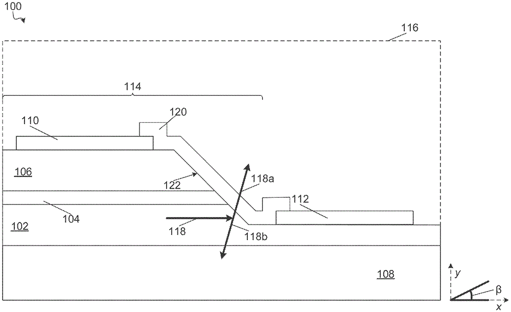
现在参考图1,示出了图示示例III族氮化物LED器件100的截面图。一个或多个半导体层,包括例如n层102、有源区104和p层106,可以外延生长在衬底108上。如上所述,p接触部110和n接触部112可以形成在器件的相同侧上。通过将从最顶层向下延伸到下面的n层102的台面结构114蚀刻到器件中以及形成分开限定的p接触部110和n接触部112,可以实现p接触部110和n接触部112之间的电隔离。LED可以被安装到子底座组件116,该子底座组件116可以包括子底座,LED利用焊料凸块被安装在该子底座上。焊料凸块可以在子底座和LED之间创建间隙。被连接的LED和子底座组件然后可以被封装在高折射率的凝胶或环氧树脂中。Referring now to FIG. 1 , a cross-sectional view illustrating an example Ill-
高折射率的凝胶或环氧树脂可以被选取以尽可能接近地匹配衬底108的折射率,因为在该器件中产生的光可以通过衬底108被提取。当光入射到两种材料之间的界面上时,折射率的差异决定了多少光在该界面处被反射,以及多少光通过它被透射。折射率的差异越大,越多的光被反射。因此,蓝宝石衬底与封装器件的高折射率的凝胶或环氧树脂的折射率之间的微小差异可以确保在器件中生成的到达衬底108的发射表面的大部分光从该器件被提取。A high index of refraction gel or epoxy can be chosen to match the index of refraction of the
光子可以在有源区104内生成。部分地由于半导体层的高折射率,从半导体有源区104提取光子到LED封装内和外部可能困难。在外延半导体层内生成的光子可以入射到半导体层与衬底108之间的界面、台面114的壁122与子底座组件116中的高折射率的凝胶或环氧树脂的界面、或者半导体层与金属接触部之间的界面。入射到三个界面中的任何一个上的光子在材料折射率方面面临阶跃。折射率中的这种阶跃可能导致入射到这种界面上的光线118被分为透射部分118a和反射部分118b。从台面114的壁122透射出的光(即,部分118a)可能不会在有用的方向上被引导出器件之外。因此,在台面114的壁122处通过透射而损耗的光可能有助于III族氮化物LED器件100的低光提取效率。Photons may be generated within
封装器件的高折射率的凝胶或环氧树脂可能导致接触部之间的半导体层之间的台面114的壁122和子底座组件116的界面处的微小的折射率差异。作为结果,入射到该区域上的大部分光可以在子底座组件的方向上透射,这可能导致大量的光学损耗。如上所述,在朝向子底座组件116的区域中提取的光可能不会从III族氮化物LED器件100中被有效地提取。The high refractive index gel or epoxy that encapsulates the device may cause small refractive index differences at the interface between the
当光通过器件传播时,它可能会受到衰减。衰减可以发生在半导体内的所有地方,但可能在界面处最大,所述界面例如在n层102和衬底108之间、在半导体层和接触部之间、在有源区104中、以及在n层102和衬底108之间存在的任何成核层中。光传播得越远,其被衰减得越多。与具有小角度β(相对于衬底108的传播角度)的光线相比,以大角度β行进穿过半导体层的光线可能需要更长的路径长度,以在与衬底108平行解析的半导体中行进给定距离。每次光线被反射时,传播角度的符号可以被反转。例如,以角度β传播的光线在反射时可以以角度−β传播。大角度β光线可以穿过有源区104更多次,并且可以在各种界面被反射更多次。每次光线被反射时,它被衰减得更多。因此,与以较浅角度β行进的光线相比,这种光线在x方向上每单位传播距离可能受到更大的衰减。因此,入射到台面114的壁122上的大部分通量(光学功率)是以浅角β入射的。对于在接触部中具有一定吸收的器件(例如,具有铝p接触部的器件),入射到台面114的壁122上的总通量的70%或更多可以以大约在-10度<β<30度的范围内的角度入射。对于具有高反射性的p接触部110(诸如纯银p接触部110)的器件,在该相同角度范围内入射到台面114的壁122上的通量的比例可以下降到约60%。As light propagates through the device, it may be attenuated. Attenuation can occur anywhere within the semiconductor, but may be greatest at interfaces, such as between n-
反射层120可以用于反射从有源区104发射的光。反射层120可以构成电介质层、金属堆叠、复合镜、或者分布式布拉格反射器(DBR)中的一个或多个。反射层120可以形成在台面114的壁122上,以最大化入射到台面114的壁122上的光的反射。反射层120可以包括透明导电层、电介质层和金属镜。复合镜可能需要金属镜直接形成在电介质层上。该金属镜可以构成贵金属,诸如例如银(Ag)或金(Au)。电介质层可以构成任何绝缘材料,诸如例如硅或氟化镁的氧化物或氮化物。The
在本领域中已知贵金属(诸如Ag)不能很好地粘合到诸如氧化硅的电介质材料。不良的粘合可能在制备过程期间引入问题并且可能降低反射层的反射率。电介质层的上表面可以在金属镜的沉积之前被粗糙化以提高粘合。表面特征的发展和粗糙表面的增加的表面积可以促进贵金属与电介质材料之间的粘合,然而,这可能不足以确保适当和/或充分的粘合。可以在电介质层和金属镜之间引入粘合层以提高上述两者之间的粘合。然而,大多数粘合剂层是光学吸收性的,并且可能负面影响反射层的反射率。因此,可以期望在提高金属镜和电介质层之间的粘合强度的同时,最小化对反射层120的总反射系数的光学影响。It is known in the art that noble metals such as Ag do not adhere well to dielectric materials such as silicon oxide. Poor adhesion can introduce problems during the manufacturing process and can reduce the reflectivity of the reflective layer. The upper surface of the dielectric layer may be roughened prior to deposition of the metal mirror to improve adhesion. The development of surface features and the increased surface area of the rough surface can promote adhesion between the noble metal and the dielectric material, however, this may not be sufficient to ensure proper and/or sufficient adhesion. An adhesion layer can be introduced between the dielectric layer and the metal mirror to improve adhesion between the two. However, most adhesive layers are optically absorptive and can negatively affect the reflectivity of the reflective layer. Therefore, it may be desirable to minimize the optical effect on the overall reflection coefficient of the
现在参考图2,示出了图示在发射层202上形成电介质层204的截面图。如上所述,发射层202可以包含第一半导体层206、有源区208和第二半导体层210。发射层202可以形成在衬底212上。衬底212可以构成诸如氧化铝的硅或晶体材料,并且可以是商业蓝宝石晶片。Referring now to FIG. 2 , a cross-sectional view illustrating the formation of
第一半导体层206可以构成任何III-V族半导体,包括镓、铝、铟和氮的二元、三元和四元合金,也被称为III族氮化物材料。例如,第一半导体层402可以构成III-V族半导体(包括但不限于AlN、AlP、AlAs、AlSb、GaN、GaP、GaAs、GaSb、InN、InP、InAs、InSb)、II-VI族半导体(包括但不限于ZnS、ZnSe、CdSe、CdTe)、IV族半导体(包括但不限于Ge、Si、SiC及其混合物或合金)。这些半导体在它们存在于的LED的典型发射波长处可以具有范围从大约2.4到大约4.1的折射率。例如,III族氮化物半导体,诸如GaN,在500nm处可以具有大约2.4的折射率,以及III族磷化物半导体,诸如InGaP,在600nm处可以具有大约3.7的折射率。在一示例中,第一半导体层402可以构成GaN。The
使用常规沉积技术(诸如MOCVD、MBE或其他外延技术)可以形成第一半导体层206。第一半导体层206可以掺杂有n型掺杂剂。The
第二半导体层210和有源区208可以构成任何III-V族半导体,包括镓、铝、铟和氮的二元、三元和四元合金,也被称为III族氮化物材料。例如,第二半导体层210和有源区210可以构成III-V族半导体(包括但不限于AlN、AlP、AlAs、AlSb、GaN、GaP、GaAs、GaSb、InN、InP、InAs、InSb)、II-VI族半导体(包括但不限于ZnS、ZnSe、CdSe、CdTe)、IV族半导体(包括但不限于Ge、Si、SiC及其混合物或合金)。这些半导体在它们存在于的LED的典型发射波长处可以具有范围从大约2.4到大约4.1的折射率。例如,III族氮化物半导体,诸如GaN,在500nm处可以具有大约2.4的折射率,以及III族磷化物半导体,诸如InGaP,在600nm处可以具有大约3.7的折射率。在一示例中,第二半导体层210和有源区208可以构成GaN。The
使用常规沉积技术(诸如MOCVD、MBE或其他外延技术)可以形成第二半导体层210和有源区208。有源区208和第二半导体层210可以与第一半导体层206一起形成,或者可以分开形成。有源区208和第二半导体层210可以构成与第一半导体层206类似的半导体材料,或者它们的组分可以变化。The
第二半导体层210可以掺杂有p型掺杂剂。因此,有源区208可以是与第一半导体层206和第二半导体层210的界面相关联的p-n二极管结。可替代地,有源区208可以包括掺杂n型、掺杂p型或未掺杂的一个或多个半导体层。在通过第一半导体层206和第二半导体层210应用合适的电压时,有源区208可以发射光。在替代的实施方式中,第一半导体层206和第二半导体层210的导电类型可以反转。即,第一半导体层206可以是p型层,并且第二半导体层210可以是n型层。The
应注意的是,发射层202可以采取任何形状。例如,发射层202可以成形为比如如上参考图1所述的台面。在另一示例中,发射层202可以与其他半导体层分段并且可以通过沟槽或隔离区与另一发射层分隔。It should be noted that the
电介质层204可以形成在发射层202的上表面214上。电介质层204可以构成一种或多种电介质材料,诸如,氧化物、氮化物或氧氮化物。在一示例中,电介质层204可以构成氧化硅。在另一示例中,电介质层204可以构成诸如氟化镁的金属氟化物。使用常规沉积技术,诸如例如CVD、等离子体增强化学气相沉积(PECVD)、MOCVD、原子层沉积(ALD)、蒸发、反应溅射、化学溶液沉积、旋涂沉积或其他类似工艺,可以形成电介质层204。电介质层204可以具有范围从大约100 nm到大约1000 nm的厚度T204。使用常规技术可以图案化和蚀刻电介质层204。
应注意,取决于发射层202的配置,电介质层204可以形成在任何表面上。例如,如上面参考图1所见的,电介质层204可以与第一半导体层206、有源区208和第二半导体层210接触。在另一示例中,电介质层204可以形成在衬底212的下表面216上。在另一示例中,电介质层204可以形成在形成于发射层202上的磷光体区(未示出)上以波长转换发射光。It should be noted that depending on the configuration of the
现在参考图3,示出了图示在电介质层204上形成中间层302的截面图。中间层302可以构成比电介质层204的材料具有更高反应焓的材料。例如,如果电介质层204包括一种或多种氧化物,则中间层302可以构成比电介质层204的材料具有更高氧化焓的一种或多种材料。在另一示例中,如果电介质层204包括氟化物,则中间层302可以构成比电介质层204的材料具有更高氟化焓的一种或多种材料。Referring now to FIG. 3 , a cross-sectional view illustrating the formation of
中间层302可以构成一种或多种金属材料的原子,诸如例如,Mg、Al、Ge、Ti、Si、Ta、Mn、W、Co、Ni、Cu、Ru、Pd、Pt和Ag。在一示例中,中间层可以构成Al,其可以具有每形成键大约550 kJ/mol到每形成键大约600 kJ/mol的氧化物形成的负热。这可能大于二氧化硅的氧化物形成的负热,二氧化硅可以是每形成键大约400 kJ/mol到每形成键大约500 kJ/mol。中间层302可以很好地粘合到电介质层204。The
使用常规沉积技术,诸如例如,CVD、PECVD、MOCVD、ALD、蒸发、反应溅射、化学溶液沉积、电镀、旋涂沉积或其他类似工艺,可以形成中间层302。中间层302可以具有范围从大约1埃到大约50埃的厚度T302。在一示例中,中间层302可以具有范围从大约5埃到大约20埃的厚度T302。
现在参考图4,示出了图示在中间层302上形成金属层402以形成反射层404的截面图。金属层402可以构成一种或多种反射光的金属材料。例如,金属层402可以构成贵金属,诸如Ru、Rh、Pd、Ag、Os、Ir、Pd和Au。金属层402可以构成上述金属中的一个或多个的堆叠。Referring now to FIG. 4 , a cross-sectional view illustrating the formation of
使用常规沉积技术,诸如例如,CVD、PECVD、MOCVD、ALD、蒸发、反应溅射、化学溶液沉积、电镀、旋涂沉积或其他类似工艺,可以形成金属层402。金属层402可以具有范围从大约50 nm到大约1000 nm的厚度T402。中间层302可以很好地粘合到金属层402。
在沉积时和/或在随后的退火步骤中,中间层302中的原子可以部分地与来自下面的电介质层204的原子反应,并且中间层302可以变得光学透明。因为中间层302可能比下面的电介质层204具有更高的反应焓,所以形成粘合剂层的原子可以断开彼此之间的键并与电介质层204中的原子形成键。例如,如果Al用于形成中间层302并且氧化硅用于形成电介质层204,则Al原子可以使电介质层204中现有的Si-O键断开并且形成单个Al-O键。在电介质层204可能已经具有Si-O-Si键的情况下,它现在可以包含Si-O-Al键,该Si-O-Al键在Si上具有可以以Al原子终止的悬空键。During deposition and/or in a subsequent annealing step, atoms in the
反应焓用作预测中间层302和电介质层204之间的键的指南。在上述示例中,由于中间层302具有更高的氧化焓,因此断开Si-O键并形成Al-O键在能量上是有利的,从而能够实现粘合。中间层302的厚度T302可以足以提高电介质层204和金属层402之间的粘合力,但也不要太厚,使得中间层302中的大部分材料不会与下面的电介质层204反应。当中间层302上的原子氧化并与电介质层204中的原子反应时,所产生的键可以产生具有大带隙的氧化物。这可以允许从有源区208发射的质子以很少至没有电阻的方式穿过电介质层204和中间层302,并从金属层402反射。换言之,由于大的带隙,电介质层204和中间层302对从有源区208发射的光可以基本透明。The reaction enthalpy is used as a guideline for predicting the bond between the
现在参考图5A-5B,示出了图示示例性反射层404的截面的透射电子显微镜(TEM)显微照片。图5A示出了发射层202、电介质层204、中间层302和金属层402。图5B是反射层404的放大图,其示出了电介质层204、中间层302和金属层402。如从图5B可见,中间层302的原子可能已经与电介质层204的原子反应以形成粘合键。Referring now to FIGS. 5A-5B , transmission electron microscopy (TEM) photomicrographs illustrating a cross-section of an exemplary
应注意,图1-5B示出了形成在外延生长的GaN上的反射层404,该反射层404可以用于在电介质层和贵金属之间需要良好粘合的所有光敏界面中。例如,反射层404可以形成在其上形成一个或多个半导体层的衬底的任何表面上。在另一示例中,反射层404可以形成在用于对从有源区发射的光进行波长转换的磷光体区上。It should be noted that Figures 1-5B show a
现在参考图6,示出了图示形成反射层404的方法的流程图。在步骤602中,可以形成真空。在步骤604中,可以使用上述方法中的一种或多种来形成电介质层204而不破坏真空。在步骤606中,可以使用上述的一种或多种方法来形成中间层302而不破坏真空。在步骤608中,可以使用上述方法中的一种或多种来形成金属层402而不破坏真空。在步骤610中,可以破坏真空。Referring now to FIG. 6, a flowchart illustrating a method of forming
现在参考图7,示出了图示形成反射层404的另一种方法的流程图。在步骤702中,可以形成真空。在步骤704中,可以使用上述方法中的一种或多种来形成电介质层204而不破坏真空。在步骤706中,可以使用上述的一种或多种方法来形成中间层302而不破坏真空。在步骤708中,可以破坏真空。在步骤710中,可以使用上述方法中的一种或多种来形成金属层402。在替代的示例中,可以在执行步骤710之前形成第二真空。Referring now to FIG. 7, a flowchart illustrating another method of forming a
现在参考图8,示出了图示形成反射层404的另一种方法的流程图。在步骤802中,可以形成真空。在步骤804中,可以使用上述方法中的一种或多种来形成电介质层204而不破坏真空。在步骤806中,可以破坏真空。在步骤808中,可以使用上述的一种或多种方法来形成中间层302。在步骤810中,可以使用上述方法中的一种或多种来形成金属层402。在替代的示例中,可以在执行步骤808或步骤810之前形成第二真空。Referring now to FIG. 8, a flowchart illustrating another method of forming a
现在参考图9,示出了图示形成反射层404的另一种方法的流程图。在步骤902中,可以形成真空。在步骤904中,可以使用上述方法中的一种或多种来形成电介质层204而不破坏真空。在步骤906中,可以使用上述的一种或多种方法来形成中间层302而不破坏真空。在步骤908中,可以破坏真空。Referring now to FIG. 9, a flowchart illustrating another method of forming a
一旦真空被破坏,天然氧化物就可以形成在中间层302的上表面上。天然氧化物可能干扰中间层302和电介质层204和/或金属层402之间的粘合。在步骤910中,中间层302的上表面可以被清洁并制备以去除天然氧化物层。清洁和制备可以包括任何常规清洗、蚀刻或平坦化工艺。Once the vacuum is broken, native oxides can form on the upper surface of the
在步骤912中,可以在使用上述方法中的一种或多种去除天然氧化物之后形成金属层402。在替代的示例中,可以在执行步骤910或步骤912之前形成第二真空。In
尽管以上以特定的组合描述了特征和元件,但是本领域普通技术人员将理解,每个特征或元件可以单独使用或与其他特征和元件以任何组合使用。另外,本文描述的方法可以在计算机可读介质中并入的计算机程序、软件或固件中实现,以由计算机或处理器执行。计算机可读介质的示例包括电子信号(通过有线或无线连接传输)和计算机可读存储介质。计算机可读存储介质的示例包括但不限于只读存储器(ROM)、随机存取存储器(RAM)、寄存器、高速缓存存储器、半导体存储设备、磁性介质(诸如内部硬盘和可移动盘)、磁光介质和光学介质(诸如CD-ROM盘和数字多功能盘(DVD))。Although features and elements are described above in specific combinations, it will be understood by those of ordinary skill in the art that each feature or element can be used alone or in any combination with other features and elements. Additionally, the methods described herein may be implemented in a computer program, software or firmware incorporated in a computer-readable medium for execution by a computer or processor. Examples of computer-readable media include electronic signals (transmitted over wired or wireless connections) and computer-readable storage media. Examples of computer-readable storage media include, but are not limited to, read only memory (ROM), random access memory (RAM), registers, cache memory, semiconductor storage devices, magnetic media (such as internal hard disks and removable disks), magneto-optical media and optical media such as CD-ROM discs and digital versatile discs (DVDs).
Claims (20)
Applications Claiming Priority (5)
| Application Number | Priority Date | Filing Date | Title |
|---|---|---|---|
| US15/881,140 US20190237629A1 (en) | 2018-01-26 | 2018-01-26 | Optically transparent adhesion layer to connect noble metals to oxides |
| US15/881140 | 2018-01-26 | ||
| EP18165085 | 2018-03-29 | ||
| EP18165085.4 | 2018-03-29 | ||
| PCT/US2019/015329 WO2019148064A1 (en) | 2018-01-26 | 2019-01-28 | Optically transparent adhesion layer to connect noble metals to oxides |
Publications (1)
| Publication Number | Publication Date |
|---|---|
| CN111971806A true CN111971806A (en) | 2020-11-20 |
Family
ID=65278478
Family Applications (1)
| Application Number | Title | Priority Date | Filing Date |
|---|---|---|---|
| CN201980022360.2A Pending CN111971806A (en) | 2018-01-26 | 2019-01-28 | Optically transparent adhesive layer for attaching noble metals to oxides |
Country Status (5)
| Country | Link |
|---|---|
| EP (1) | EP3743949A1 (en) |
| KR (1) | KR20200121815A (en) |
| CN (1) | CN111971806A (en) |
| TW (1) | TWI703740B (en) |
| WO (1) | WO2019148064A1 (en) |
Families Citing this family (2)
| Publication number | Priority date | Publication date | Assignee | Title |
|---|---|---|---|---|
| US20230155070A1 (en) * | 2021-11-12 | 2023-05-18 | Lumileds Llc | Thin-film led array with low refractive index patterned structures and reflector |
| US12490570B2 (en) | 2021-11-12 | 2025-12-02 | Lumileds Singapore Pte. Ltd. | Thin-film LED array with low refractive index patterned structures |
Citations (12)
| Publication number | Priority date | Publication date | Assignee | Title |
|---|---|---|---|---|
| JP2000232253A (en) * | 1999-02-12 | 2000-08-22 | Mitsubishi Chemicals Corp | Semiconductor light emitting device |
| US20070058059A1 (en) * | 2005-09-07 | 2007-03-15 | Toyoda Gosei Co., Ltd. | Solid-state element device |
| US20100123153A1 (en) * | 2008-11-18 | 2010-05-20 | Jin-Ywan Lin | Light-emitting device |
| US20100154213A1 (en) * | 2008-12-19 | 2010-06-24 | Tohoku University | Method for forming copper interconnection structures |
| JP2012114130A (en) * | 2010-11-22 | 2012-06-14 | Panasonic Corp | Light-emitting element |
| KR20130068448A (en) * | 2011-12-15 | 2013-06-26 | 한국전자통신연구원 | Light emitting diode |
| EP2768036A2 (en) * | 2013-02-18 | 2014-08-20 | Kabushiki Kaisha Toshiba | Semiconductor light emitting device and method for manufacturing the same |
| US20150280078A1 (en) * | 2014-03-31 | 2015-10-01 | SemiLEDs Optoelectronics Co., Ltd. | White flip chip light emitting diode (fc led) and fabrication method |
| US20150333241A1 (en) * | 2014-05-19 | 2015-11-19 | Epistar Corporation | Optoelectronic device and method for manufacturing the same |
| US20150372208A1 (en) * | 2014-06-23 | 2015-12-24 | Seoul Viosys Co., Ltd. | Light emitting device |
| US20160365496A1 (en) * | 2015-06-10 | 2016-12-15 | Lextar Electronics Corporation | Light-emitting device |
| US20170186917A1 (en) * | 2014-06-10 | 2017-06-29 | Semicon Light Co., Ltd. | Semiconductor light-emitting element |
Family Cites Families (2)
| Publication number | Priority date | Publication date | Assignee | Title |
|---|---|---|---|---|
| JP4330476B2 (en) * | 2004-03-29 | 2009-09-16 | スタンレー電気株式会社 | Semiconductor light emitting device |
| US8680556B2 (en) * | 2011-03-24 | 2014-03-25 | Cree, Inc. | Composite high reflectivity layer |
-
2019
- 2019-01-28 CN CN201980022360.2A patent/CN111971806A/en active Pending
- 2019-01-28 KR KR1020207024642A patent/KR20200121815A/en not_active Ceased
- 2019-01-28 EP EP19703229.5A patent/EP3743949A1/en active Pending
- 2019-01-28 WO PCT/US2019/015329 patent/WO2019148064A1/en not_active Ceased
- 2019-01-28 TW TW108103146A patent/TWI703740B/en active
Patent Citations (12)
| Publication number | Priority date | Publication date | Assignee | Title |
|---|---|---|---|---|
| JP2000232253A (en) * | 1999-02-12 | 2000-08-22 | Mitsubishi Chemicals Corp | Semiconductor light emitting device |
| US20070058059A1 (en) * | 2005-09-07 | 2007-03-15 | Toyoda Gosei Co., Ltd. | Solid-state element device |
| US20100123153A1 (en) * | 2008-11-18 | 2010-05-20 | Jin-Ywan Lin | Light-emitting device |
| US20100154213A1 (en) * | 2008-12-19 | 2010-06-24 | Tohoku University | Method for forming copper interconnection structures |
| JP2012114130A (en) * | 2010-11-22 | 2012-06-14 | Panasonic Corp | Light-emitting element |
| KR20130068448A (en) * | 2011-12-15 | 2013-06-26 | 한국전자통신연구원 | Light emitting diode |
| EP2768036A2 (en) * | 2013-02-18 | 2014-08-20 | Kabushiki Kaisha Toshiba | Semiconductor light emitting device and method for manufacturing the same |
| US20150280078A1 (en) * | 2014-03-31 | 2015-10-01 | SemiLEDs Optoelectronics Co., Ltd. | White flip chip light emitting diode (fc led) and fabrication method |
| US20150333241A1 (en) * | 2014-05-19 | 2015-11-19 | Epistar Corporation | Optoelectronic device and method for manufacturing the same |
| US20170186917A1 (en) * | 2014-06-10 | 2017-06-29 | Semicon Light Co., Ltd. | Semiconductor light-emitting element |
| US20150372208A1 (en) * | 2014-06-23 | 2015-12-24 | Seoul Viosys Co., Ltd. | Light emitting device |
| US20160365496A1 (en) * | 2015-06-10 | 2016-12-15 | Lextar Electronics Corporation | Light-emitting device |
Also Published As
| Publication number | Publication date |
|---|---|
| WO2019148064A1 (en) | 2019-08-01 |
| EP3743949A1 (en) | 2020-12-02 |
| TWI703740B (en) | 2020-09-01 |
| KR20200121815A (en) | 2020-10-26 |
| TW201933623A (en) | 2019-08-16 |
Similar Documents
| Publication | Publication Date | Title |
|---|---|---|
| JP4907842B2 (en) | Light emitting diode with planar omnidirectional reflector | |
| US7985979B2 (en) | Semiconductor light emitting device with light extraction structures | |
| CN102742038B (en) | Light-emitting diode with dielectric mirror in lateral configuration | |
| US8093607B2 (en) | Optoelectronic semiconductor component | |
| CN101673794B (en) | Light emitting device | |
| CN101645482B (en) | Nitride semiconductor light emitting device and method of manufacturing the same | |
| CN102804417B (en) | Contacts for semiconductor light emitting devices | |
| CN100546060C (en) | Inverted trapezoidal microstructure high-brightness light-emitting diode and manufacturing method thereof | |
| CN101853910A (en) | Light emitting element | |
| JP2019204981A (en) | Device having porous reflective contact | |
| CN101740684A (en) | Light emitting element | |
| US20240250218A1 (en) | Optically transparent adhesion layer to connect noble metals to oxides | |
| TWI703740B (en) | Optically transparent adhesion layer to connect noble metals to oxides | |
| JP5245529B2 (en) | Semiconductor light emitting device and method for manufacturing semiconductor light emitting device | |
| JP2006339384A (en) | LIGHT EMITTING ELEMENT, ITS MANUFACTURING METHOD, AND LIGHTING DEVICE USING THE LIGHT EMITTING ELEMENT |
Legal Events
| Date | Code | Title | Description |
|---|---|---|---|
| PB01 | Publication | ||
| PB01 | Publication | ||
| SE01 | Entry into force of request for substantive examination | ||
| SE01 | Entry into force of request for substantive examination |