CN111952251A - Integrated circuit package and method of forming the same - Google Patents
Integrated circuit package and method of forming the same Download PDFInfo
- Publication number
- CN111952251A CN111952251A CN202010397863.2A CN202010397863A CN111952251A CN 111952251 A CN111952251 A CN 111952251A CN 202010397863 A CN202010397863 A CN 202010397863A CN 111952251 A CN111952251 A CN 111952251A
- Authority
- CN
- China
- Prior art keywords
- package
- dummy die
- encapsulant
- package element
- die
- Prior art date
- Legal status (The legal status is an assumption and is not a legal conclusion. Google has not performed a legal analysis and makes no representation as to the accuracy of the status listed.)
- Granted
Links
Images


Classifications
-
- H10W42/121—
-
- H10P54/00—
-
- H10P95/062—
-
- H10W20/49—
-
- H10W70/095—
-
- H10W70/611—
-
- H10W70/635—
-
- H10W72/071—
-
- H10W74/01—
-
- H10W74/012—
-
- H10W74/014—
-
- H10W74/016—
-
- H10W74/10—
-
- H10W74/117—
-
- H10W74/131—
-
- H10W90/00—
-
- H10W72/0198—
-
- H10W72/072—
-
- H10W72/073—
-
- H10W72/222—
-
- H10W72/227—
-
- H10W72/241—
-
- H10W72/248—
-
- H10W72/252—
-
- H10W72/354—
-
- H10W72/923—
-
- H10W72/944—
-
- H10W72/952—
-
- H10W74/142—
-
- H10W74/15—
-
- H10W90/28—
-
- H10W90/297—
-
- H10W90/722—
-
- H10W90/724—
-
- H10W90/732—
-
- H10W90/734—
Landscapes
- Engineering & Computer Science (AREA)
- Microelectronics & Electronic Packaging (AREA)
- Power Engineering (AREA)
- Physics & Mathematics (AREA)
- Condensed Matter Physics & Semiconductors (AREA)
- General Physics & Mathematics (AREA)
- Computer Hardware Design (AREA)
- Manufacturing & Machinery (AREA)
- Structures Or Materials For Encapsulating Or Coating Semiconductor Devices Or Solid State Devices (AREA)
- Ceramic Engineering (AREA)
Abstract
本申请的实施例提供了集成电路的封装件以及形成封装件的方法,方法包括:将第二封装元件接合至第一封装元件,将第三封装元件接合至第一封装元件,将伪管芯附接至第一封装元件,将第二封装元件、第三封装元件和伪管芯包封在密封剂中,并且执行平坦化工艺以使第二封装元件的顶面与密封剂的顶面齐平。在平坦化工艺之后,密封剂的上部与伪管芯重叠。锯切穿过伪管芯以将伪管芯分离为第一伪管芯部分和第二伪管芯部分。密封剂的上部被锯切穿过。
Embodiments of the present application provide a package for an integrated circuit and a method for forming the package, the method comprising: bonding a second package element to a first package element, bonding a third package element to the first package element, bonding a dummy die Attaching to the first package element, encapsulating the second package element, the third package element and the dummy die in the encapsulant, and performing a planarization process to align the top surface of the second package element with the top surface of the encapsulant flat. After the planarization process, the upper portion of the encapsulant overlaps the dummy die. Saw cutting through the dummy die to separate the dummy die into a first dummy die portion and a second dummy die portion. The upper part of the sealant is sawed through.
Description
技术领域technical field
本申请的实施例涉及集成电路的封装件及其形成方法。Embodiments of the present application relate to packages of integrated circuits and methods of forming the same.
背景技术Background technique
自集成电路(IC)的发展以来,由于各种电子元件(即晶体管、二极管、电阻器、电容器等)的集成密度的不断改进,半导体行业经历了持续快速的增长。大部分情况下,集成密度的提高来自最小部件尺寸的不断减小,这使得更多的元件可以集成到给定区域中。Since the development of integrated circuits (ICs), the semiconductor industry has experienced continued rapid growth due to continuous improvements in the integration density of various electronic components (ie, transistors, diodes, resistors, capacitors, etc.). In most cases, the increase in integration density comes from the continuous reduction of minimum feature size, which allows more components to be integrated into a given area.
因为集成的元件所占据的区域基本上在半导体晶圆的表面上,所以这些集成改进基本上本质是二维(2D)。集成电路的增加的密度和相应的面积减小通常已经超过了将集成电路芯片直接接合到衬底上的能力。中介层已用于将焊球的接触区域从芯片的接触区域重分布到中介层的较大区域。此外,中介层已经允许包括多个芯片的三维(3D)封装件。还开发了其他封装件包以并入3D方面。These integration improvements are essentially two-dimensional (2D) in nature because the area occupied by the integrated components is essentially on the surface of the semiconductor wafer. The increased density and corresponding reduction in area of integrated circuits has generally outpaced the ability to directly bond integrated circuit chips to substrates. Interposers have been used to redistribute the contact area of the solder balls from the contact area of the chip to a larger area of the interposer. In addition, interposers have allowed three-dimensional (3D) packages that include multiple chips. Other package packages have also been developed to incorporate 3D aspects.
发明内容SUMMARY OF THE INVENTION
根据本发明的一方面,提供了一种形成封装件的方法,包括:将第二封装元件接合至第一封装元件;将第三封装元件接合至第一封装元件;将伪管芯附接至第一封装元件;将第二封装元件、第三封装元件和伪管芯包封在密封剂中;执行平坦化工艺以使第二封装元件的顶面与密封剂的顶面齐平,其中,在平坦化工艺之后,密封剂的上部与伪管芯重叠;以及锯切穿过伪管芯以将伪管芯分离为第一伪管芯部分和第二伪管芯部分,其中,密封剂的上部被锯切穿过。According to an aspect of the present invention, there is provided a method of forming a package comprising: bonding a second package element to a first package element; bonding a third package element to the first package element; attaching a dummy die to a first package element; encapsulating a second package element, a third package element, and a dummy die in an encapsulant; performing a planarization process to make a top surface of the second package element flush with a top surface of the encapsulant, wherein, After the planarization process, an upper portion of the encapsulant overlaps the dummy die; and sawing through the dummy die to separate the dummy die into a first dummy die portion and a second dummy die portion, wherein the encapsulant's The upper part is sawed through.
根据本发明的另一方面,提供了一种形成封装件的方法,包括:将第一封装元件接合至第二封装元件,其中,第一封装元件包括器件管芯;将伪管芯附接至第二封装元件,其中,伪管芯包括凹槽;将第一封装元件和伪管芯包封在密封剂中,其中,密封剂包括填充凹槽的部分;以及使用刀片执行分割工艺以形成封装件,其中,封装件包括第一封装元件、第二封装元件的部分和伪管芯的部分,并且其中,刀片切割穿过位于凹槽中的密封剂的部分。According to another aspect of the present invention, there is provided a method of forming a package comprising: bonding a first package element to a second package element, wherein the first package element includes a device die; and attaching a dummy die to a second packaging element, wherein the dummy die includes a groove; encapsulating the first packaging element and the dummy die in an encapsulant, wherein the encapsulant includes a portion filling the groove; and performing a dicing process using a blade to form the package , wherein the package includes the first package element, a portion of the second package element, and a portion of the dummy die, and wherein the blade cuts through the portion of the encapsulant located in the groove.
根据本发明的又一方面,提供了一种集成电路的封装件,封装件包括:第一封装元件;第二封装元件,位于第一封装元件上方并接合至第一封装元件;伪管芯,位于第一封装元件上方并且附接至第一封装元件,其中,伪管芯有第一顶表面和低于第一顶表面的第二顶表面;以及密封剂,将伪管芯包封在密封剂中,其中,密封剂包括与伪管芯的第二顶面重叠的第一部分,并且通过密封剂暴露伪管芯的第一顶面。According to yet another aspect of the present invention, an integrated circuit package is provided, the package includes: a first package element; a second package element located above the first package element and bonded to the first package element; a dummy die, overlying and attached to the first packaging element, wherein the dummy die has a first top surface and a second top surface lower than the first top surface; and an encapsulant encapsulating the dummy die in the sealing wherein the encapsulant includes a first portion overlapping the second top surface of the dummy die, and the first top surface of the dummy die is exposed through the encapsulant.
附图说明Description of drawings
当结合附图进行阅读时,根据下面详细的描述可以最好地理解本发明的各个实施例。应该注意,根据工业中的标准实践,各种部件没有被按比例绘制。实际上,为了清楚的讨论,各种部件的尺寸可以被任意增加或减少。Various embodiments of the invention are best understood from the following detailed description when read in conjunction with the accompanying drawings. It should be noted that in accordance with standard practice in the industry, the various components are not drawn to scale. In fact, the dimensions of the various components may be arbitrarily increased or decreased for clarity of discussion.
图1至图5、图6A、图6B、图6C、图6D、图6E、图6F和图7至图14是根据一些实施例的形成封装件结构的示例工艺中的截面图和平面图。1-5, 6A, 6B, 6C, 6D, 6E, 6F, and 7-14 are cross-sectional and plan views in example processes of forming package structures according to some embodiments.
图15至图19是根据一些实施例的形成封装件结构的示例工艺中的截面图和平面图。15-19 are cross-sectional and plan views in an example process of forming a package structure in accordance with some embodiments.
图20A至图20F示出了根据一些实施例的封装件结构的平面图。20A-20F illustrate plan views of package structures in accordance with some embodiments.
图21A至图21F示出了根据一些实施例的封装件结构的平面图。21A-21F illustrate plan views of package structures in accordance with some embodiments.
图22A至图22D示出了根据一些实施例的封装件结构的平面图。22A-22D illustrate plan views of package structures in accordance with some embodiments.
图23示出了根据一些实施例的用于形成封装件结构的工艺流程。23 illustrates a process flow for forming a package structure in accordance with some embodiments.
具体实施方式Detailed ways
以下公开内容提供了许多不同实施例或实例,用于实现所提供主题的不同特征。以下将描述组件和布置的具体实例以简化本发明。当然,这些仅是实例并且不意欲限制本发明。例如,在以下描述中,在第二部件上方或上形成第一部件可以包括第一部件和第二部件形成为直接接触的实施例,也可以包括形成在第一部件和第二部件之间的附加部件使得第一部件和第二部件不直接接触的实施例。而且,本发明在各个实例中可以重复参考数字和/或字母。这种重复仅是为了简明和清楚,其自身并不表示所论述的各个实施例和/或配置之间的关系。The following disclosure provides many different embodiments or examples for implementing different features of the presented subject matter. Specific examples of components and arrangements are described below to simplify the present disclosure. Of course, these are only examples and are not intended to limit the invention. For example, in the following description, forming the first part over or on the second part may include embodiments in which the first part and the second part are formed in direct contact, and may also include an embodiment in which the first part and the second part are formed in direct contact. An embodiment in which the additional part is such that the first part and the second part are not in direct contact. Furthermore, the present disclosure may repeat reference numerals and/or letters in various instances. This repetition is for brevity and clarity only and does not in itself represent a relationship between the various embodiments and/or configurations discussed.
此外,为了便于描述,本文中可以使用诸如“在…下方”、“在…下面”、“下部”、“在…上面”、“上部”等的空间关系术语,以描述如图中所示的一个元件或部件与另一元件或部件的关系。除了图中所示的方位外,空间关系术语旨在包括器件在使用或操作过程中的不同方位。装置可以以其他方式定位(旋转90度或在其他方位),并且在本文中使用的空间关系描述符可以同样地作相应地解释。Furthermore, for ease of description, spatially relative terms such as "below", "below", "lower", "above", "upper", etc. may be used herein to describe the figures as shown in the figures. The relationship of one element or component to another element or component. In addition to the orientation shown in the figures, spatially relative terms are intended to encompass different orientations of the device during use or operation. The device may be otherwise oriented (rotated 90 degrees or at other orientations) and the spatially relative descriptors used herein interpreted accordingly.
根据各种实施例,提供了包括伪管芯的封装件结构及其形成方法。根据一些实施例示出了封装件结构的形成中的中间阶段。讨论了一些实施例的一些变型。贯穿各种视图和说明性实施例,类似的参考标号用于指示类似的元件。根据本公开的一些实施例,包括伪管芯的封装件结构被放置在有源管芯附近以减小封装件结构的翘曲。通过减小有源管芯和中介层之间的冷接头的可能性,封装件结构的翘曲的这种减小使得封装件结构更可靠。根据一些实施例,伪管芯沿着封装件结构的外围放置,例如在划线区域中或附近。因此,当封装件结构被分割时,伪管芯被锯穿。留下模制化合物的层与伪管芯重叠,以防止分割中的伪管芯碎裂。According to various embodiments, package structures including dummy dies and methods of forming the same are provided. Intermediate stages in the formation of package structures are shown in accordance with some embodiments. Some variations of some embodiments are discussed. Like reference numerals are used to designate like elements throughout the various views and illustrative embodiments. According to some embodiments of the present disclosure, a package structure including a dummy die is placed near the active die to reduce warpage of the package structure. This reduction in warpage of the package structure makes the package structure more reliable by reducing the likelihood of cold joints between the active die and the interposer. According to some embodiments, the dummy die is placed along the periphery of the package structure, eg, in or near the scribe line area. Therefore, when the package structure is singulated, the dummy dies are sawed through. The layer of molding compound is left to overlap the dummy die to prevent fragmentation of the dummy die during singulation.
将关于特定上下文对实施例进行描述,即,使用衬底上晶圆上芯片(CoWoS)工艺的管芯-中介层-衬底堆叠封装件。然而,其他实施例也可以应用于其他封装件,诸如管芯-管芯-衬底堆叠封装件以及其他工艺。本文讨论的实施例将提供示例,以使得能够进行或使用本公开的主题,并且本领域普通技术人员将容易理解可以进行的修改同时保持在不同实施例的预期范围内。尽管方法实施例可以被讨论为以特定顺序执行,但是其他的方法实施例可以以任何逻辑顺序执行。Embodiments will be described with respect to a specific context, namely, a die-interposer-substrate stacked package using a chip-on-wafer-on-substrate (CoWoS) process. However, other embodiments may also be applied to other packages, such as die-die-substrate stacked packages and other processes. The embodiments discussed herein will provide examples of how to make or use the subject matter of the present disclosure, and those of ordinary skill in the art will readily appreciate the modifications that can be made while remaining within the intended scope of the different embodiments. Although method embodiments may be discussed as being performed in a particular order, other method embodiments may be performed in any logical order.
图1至图5、图6A、图6B、图6C、图6D、图6E、图6F和图7至图14示出了根据本公开的一些实施例的形成封装件结构的中间阶段的截面图和平面图(诸如顶视图)。相应的工艺也示意性地反映在图23所示的工艺流程中。1-5, 6A, 6B, 6C, 6D, 6E, 6F, and 7-14 illustrate cross-sectional views of intermediate stages of forming a package structure according to some embodiments of the present disclosure and floor plans (such as top views). The corresponding process is also schematically reflected in the process flow shown in FIG. 23 .
图1示出了根据一些实施例的晶圆10的形成,晶圆10包括封装元件28(图2)。封装元件28可以是器件管芯、封装件等。封装元件28可以包括任何数量的管芯、衬底、晶体管、有源器件、无源器件等。在一个实施例中,封装元件28可以包括衬底20,衬底20可以是块状半导体衬底、绝缘体上半导体(SOI)衬底、多层半导体衬底等。半导体衬底由半导体材料形成,半导体材料可以是硅、锗、包括硅锗、碳化硅、砷化镓、磷化镓、磷化铟、砷化铟和/或锑化铟的化合物半导体;包括SiGe、GaAsP、AlInAs、AlGaAs、GaInAs、GaInP和/或GaInAsP的合金半导体;或其组合。也可以使用其他衬底,诸如多层衬底或梯度衬底。衬底20可以是掺杂的或非掺杂的。诸如晶体管、电容器、电阻器、二极管等的器件可以形成在半导体衬底20的有源表面22中和/或上方。FIG. 1 illustrates the formation of
封装元件28可以包括互连结构24,互连结构24包括一个或多个介电层和形成在有源表面22上的相应的金属化图案。诸如通过使用通孔和/或迹线,介电层中的金属化图案可以路由器件之间的电信号,并且还可以包括各种电器件,诸如电容器、电阻器、电感器等。各种器件和金属化图案可以互连以执行一个或多个功能。功能可以包括存储器结构、处理结构、传感器、放大器、功率分配、输入/输出电路等。另外,在互连结构24中和/或上形成诸如导电柱(例如,包括诸如铜的金属)电连接件26,以提供到电路和器件的外部电连接。根据一些实施例,电连接件26从互连结构24突出以形成柱结构。
根据本公开的一些实施例,可以在互连结构24中形成多个金属化间介电(IMD)层。例如,通过本领域已知的任何合适方法(诸如旋涂、化学气相沉积(CVD)、等离子体增强CVD(PECVD)、高密度等离子体化学气相沉积(HDP-CVD)等),IMD层可以由低K介电材料(诸如磷硅酸盐玻璃(PSG)、硼磷硅酸盐玻璃(BPSG)、氟硅酸盐玻璃(FSG)、SiOxCy)、旋涂玻璃、旋涂聚合物、硅碳材料、其化合物、其复合材料、其组合等形成。可以例如通过使用光刻技术在IMD层上沉积和图案化光刻胶材料以暴露IMD层中要成为金属化图案的部分,在IMD层中形成金属化图案。可以使用诸如各向异性干法蚀刻工艺等的蚀刻工艺来在IMD层中产生与IMD层的暴露部分相对应的凹槽和/或开口。凹槽和/或开口可以衬有扩散阻挡层并且填充有导电材料。扩散阻挡层可以包括通过原子层沉积(ALD)等沉积的氮化钽、钽、氮化钛、钛、钨钴等或其组合的一层或多层。金属化图案的导电材料可以包括通过CVD、物理气相沉积(PVD)等沉积的铜、铝、钨、银及其组合等。诸如通过使用化学机械抛光(CMP)工艺,可以去除IMD层上的任何过量的扩散阻挡层和/或导电材料。According to some embodiments of the present disclosure, a plurality of intermetallic dielectric (IMD) layers may be formed in
在图2中,晶圆10被分割成单独的封装元件28。通常,封装元件28包含相同的电路(诸如器件和金属化图案),尽管管芯可以具有不同的电路。可以通过锯片锯切、激光切割等来进行分割。In FIG. 2 ,
每个封装元件28可以包括一个或多个逻辑管芯(例如,中央处理单元、图形处理单元、现场可编程门阵列(FPGA)、片上系统(SOC)管芯、微控制器等))、内存管芯(例如,动态随机存取存储器(DRAM)芯片、静态随机存取存储器(SRAM)芯片等)、电源管理芯片(例如,电源管理集成电路(PMIC)芯片)、射频(RF)芯片、传感器芯片、微机电系统(MEMS)芯片、信号处理芯片(例如,数字信号处理(DSP)芯片)、前端芯片(例如,模拟前端(AFE)芯片)等、或其组合。Each
图3至图5和图7至图14示出了封装封装元件和伪管芯中的中间阶段的截面图,封装元件和伪管芯被接合到其他封装元件。各个工艺被示出为如图23所示的工艺流程400。在图3至图5和7至图14中,中介层用作封装元件36的示例,在其上接合有其他封装元件。应当理解,诸如封装衬底(有芯的或无芯的)、封装件等的其他类型的封装元件也可以用作封装元件36。3-5 and 7-14 show cross-sectional views of intermediate stages in packaging package components and dummy dies that are bonded to other package components. The various processes are shown as process flow 400 as shown in FIG. 23 . In FIGS. 3-5 and 7-14, an interposer is used as an example of a
图3示出了根据一些实施例的封装元件32,在工艺期间包括一个或多个封装元件36。封装元件32可以是中介晶圆,其内没有有源器件(诸如晶体管和二极管)和无源器件(诸如电阻器、电容器、电感器等)。封装元件32也可以是包括有源和/或无源器件的器件晶圆。衬底34可以是半导体衬底或介电衬底。当是半导体衬底时,衬底34可以是体半导体衬底、绝缘体上硅(SOI)衬底、多层半导体衬底等。衬底34的半导体材料可以是硅、锗,包括硅锗、碳化硅、砷化镓、磷化镓、磷化铟、砷化铟和/或锑化铟的化合物半导体;包括SiGe、GaAsP、AlInAs、AlGaAs、GaInAs、GaInP和/或GaInAsP的合金半导体;或其组合。也可以使用诸如多层衬底或梯度衬底的其他衬底。衬底34可以是掺杂的或未掺杂的。封装元件32也可以是封装衬底,其可以包括有芯衬底或者可以是无芯衬底。FIG. 3
贯通孔(TV)38形成为从衬底34的第一表面37延伸到衬底34中。当衬底34是硅衬底时,TV 38有时也称为衬底通孔或硅通孔。可以通过例如通过蚀刻、铣削、激光技术、其组合等在衬底34中形成凹槽来形成TV 38。可以诸如通过使用氧化工艺或保形沉积工艺在凹槽中形成薄的介电材料。可以诸如通过CVD、ALD、PVD、热氧化,其组合等将薄的阻挡层保形地沉积在衬底34的前侧上方和开口中。可以将导电材料沉积在薄阻挡层上方和开口中。可以通过电化学镀覆工艺、CVD、ALD、PVD、其组合等形成导电材料。导电材料的示例是铜、钨、铝、银、金、其组合等。导电材料和阻挡层的过量部分通过例如CMP从衬底34的前侧去除。因此,TV 38可以包括导电材料以及在导电材料和衬底34之间的薄的阻挡层。Through vias (TVs) 38 are formed extending from the
重分布结构40形成在衬底34的第一表面37上方,并且用于将集成电路器件(如果有的话)和/或TV 38一起与外部器件外部器件和/或电连接到外部器件。重分布结构40可以包括一个或多个介电层以及在介电层中的相应的金属化图案。金属化图案可以包括通孔和/或迹线,以将任何器件和/或TV 38一起与外部器件互连和/或互连到外部器件。金属化图案有时称为重分布线(RDL)。介电层可以包括氧化硅、氮化硅、碳化硅、氮氧化硅、低K介电材料(诸如PSG、BPSG、FSG、SiOxCy、玻璃旋涂、聚合物旋涂、硅碳材料)、其化合物、其复合物、其组合等。可以通过本领域已知的任何合适的方法来沉积介电层,诸如旋涂、CVD、PECVD、HDP-CVD等。可以例如通过使用光刻技术在介电层上沉积和图案化光刻胶材料以暴露电介质层的要成为金属化图案的部分,来在介电层中形成金属化图案。可以使用诸如各向异性干蚀刻工艺的蚀刻工艺来在介电层中产生与介电层的暴露部分相对应的凹槽和/或开口。凹槽和/或开口可以衬有扩散阻挡层并且填充有导电材料。扩散阻挡层可以包括通过ALD等沉积的TaN、Ta、TiN、Ti、Ti、CoW等的一层或多层,并且导电材料可以包括铜、铝、钨、银及其组合。通过CVD、PVC等沉积。可以例如通过使用CMP工艺去除介电层上的任何过量的扩散阻挡层和/或导电材料。A
电连接件41/42在导电焊盘上的重分布结构40的顶表面处形成。根据一些实施例,导电焊盘包括凸块下金属(UBM)。在所示的实施例中,焊盘形成在重分布结构40的介电层的开口中。在另一个实施例中,焊盘(UBM)可以延伸穿过重分布结构40的介电层的开口并且还延伸穿过重分布结构40的顶面。
根据一些实施例,电连接件41/42包括具有金属帽层42的金属柱41,金属帽层42在金属柱41上方,金属帽层42可以是焊料帽。电连接件41/42包括柱41和帽层42,柱41和帽层42有时被称为微凸块41/42。根据一些实施例,金属柱41包括诸如铜、铝、金、镍、钯等、或其组合的导电材料并且可以通过溅射、印刷、电镀、化学镀、CVD等形成。金属柱41可以是无焊料的并且具有基本上垂直的侧壁。根据一些实施例,金属帽层42形成在金属柱41的顶部上。金属帽层42可以包括镍、锡、锡铅、金、铜、银、钯、铟、镍-钯-金、镍-金等或其组合并且可以通过电镀工艺形成。According to some embodiments, the
在图4中,封装元件28和封装元件44例如通过倒装芯片接合经过封装元件28/44上的电连接件41/42和金属柱43接合到封装元件36的第一侧,以形成导电接头39。在图23中所示的工艺流程400中,相应的工艺被示出为工艺402。金属柱43可以类似于金属柱41,并且在此不再重复描述。封装元件28和封装元件44可以使用例如拾取-放置工具放置在电连接件41/42上。In Figure 4,
封装元件44可以通过与上述关于封装元件28类似的工艺来形成。根据一些实施例,封装元件44包括一个或多个存储管芯,诸如存储管芯的堆叠件(例如,DRAM管芯、SRAM管芯、高带宽存储器(HBM)管芯、混合存储立方体(HMC)管芯、低功耗(LP)双倍数据速率(DDR)存储器模块等)。在存储器管芯的堆叠件实施例中,例如,封装元件44可以包括存储器管芯和存储器控制器,诸如具有存储器控制器的四个或八个存储器管芯的堆叠件。而且,根据一些实施例,封装元件44可以是不同的尺寸(例如,不同的高度和/或表面积),并且在其他实施例中,封装元件44可以是相同的尺寸(例如,相同的高度和/或表面积)。
根据一些实施例,封装元件44可以具有与封装元件28的高度类似的高度(如图4所示),或者根据一些实施例,封装元件28和封装元件44可以是不同的高度。According to some embodiments,
封装元件44包括主体46、互连结构48和电连接件50。封装元件44的主体46可以包括任何数量的管芯、衬底、晶体管、有源器件、无源器件等。在一个实施例中,主体46可以包括块状半导体衬底、绝缘体上半导体(SOI)衬底、多层半导体衬底等。主体46的半导体材料可以选自衬底20的类似候选材料和结构。诸如晶体管、电容器、电阻器、二极管等的器件可以形成在有源表面中和/或上。
包括一个或多个介电层的互连结构48和相应的金属化图案形成在封装元件44的有源表面上。诸如通过使用通孔和/或迹线,介电层中的金属化图案可以在两个或多个介电层之间路由电信号,并且还可以包含各种电器件,诸如电容器、电阻器、电感器等。各种器件和金属化图案可以互连以执行电功能。另外,在互连结构48中和/或上形成电连接件50,诸如导电柱(例如,包括诸如铜之类的金属),以提供到电路和器件的外部电连接。根据一些实施例,电连接件50从互连结构48突出以形成在将封装元件44接合到其他结构时使用的柱结构。本领域普通技术人员将理解,提供以上示例是为了说明性目的。对于给定的应用可以适当地使用其他电路。
导电接头39分别通过互连结构48和24以及电连接件50和26将封装元件28和44中的电路电耦合到封装元件36中的TV 38。
封装元件28和44与封装元件36之间的接合可以是焊料接合或者是直接的金属与金属(诸如铜与铜)接合。在一个实施例中,封装元件28和封装元件44通过回流工艺接合到封装元件36。在此回流工艺中,电连接件41/42/43分别与电连接件26和50接触,并且重分布结构40的焊盘与封装元件28物理和电耦合并且封装元件44与封装元件36物理和电耦合。The bond between
在图4和后续附图中,分别示出了用于形成第一封装件和第二封装件的第一封装件区域45A和第二封装件区域45B。划线区域47在相邻的封装件区域之间。如图4所示,第一管芯28和多个第二管芯44附接在第一封装件区域45A和第二封装件区域45B的每一个中。In FIG. 4 and subsequent figures, a
在图5中,将底部填充材料52分配到封装元件28/44与重分布结构40的相应下部之间的间隙中。在图23中所示的工艺流程400中,相应的工艺示出为工艺404。底部填充材料52可以沿着封装元件28和封装元件44的侧壁向上延伸。底部填充材料52可以是任何可接受的材料,诸如聚合物、环氧树脂、模制底部填充材料等。底部填充材料52可以在附接封装元件28和封装元件44之后通过毛细管流动工艺形成。In FIG. 5 ,
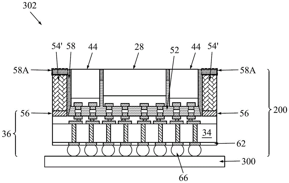
图6A、图6B、图6C、图6D、图6E和图6F示出了封装件结构的平面图,该封装件结构包括粘附至封装元件36的伪管芯54。图7是示出了封装件结构中的伪管芯54的截面图。图7是图6C的线A-A的平面图。可以通过使用例如拾取-放置工具将伪管芯54放置在封装元件36上。在图6A、图6B、图6C、图6D、图6E和图6F中,“HBM”和“SOC”分别被标记为示例封装元件44和封装元件28。应当理解,只要适用封装元件44和封装元件28可以是任何其他类型的器件。FIGS. 6A , 6B, 6C, 6D, 6E, and 6F show plan views of a package structure including dummy die 54 adhered to package
在图6A中,伪管芯54附接在划线区域47中,并且具有沿着沿第一方向(例如,图6A的垂直方向)的划线区域47延伸的长度方向。在图6B中,伪管芯54附接在相同的区域45A和/或45B的相邻的封装元件44之间。在图6C中,伪管芯54附接在划线区域47中,并且沿着沿第一方向和第二方向(例如,图6C的垂直和水平方向)的划线区域47延伸并且还插入在相同的区域45A和/或45B的相邻的封装元件44之间。In FIG. 6A , dummy die 54 is attached in
在图6D中,伪管芯54连接在相同的区域45A和/或45B的相邻的封装元件44之间,并且不在划线区域47中而是在划线区域47附近。在图6E中,除了伪管芯54还附接在与封装元件44相邻的区域45A和/或45B的拐角附近之外,伪管芯54的配置与图6D的配置类似。此外,在该实施例中,伪管芯54不在划线区域47中而是在划线区域47附近。在图6F中,伪管芯54附接在与封装元件44相邻的区域45A和/或45B的拐角附近,并且不在划线区域中而是在划线区域47附近。In FIG. 6D , dummy dies 54 are connected between
放置在划线区域47中或附近的伪管芯54能够有助于防止在第一和第二封装件区域45A和45B中的封装件被分割(参见图13)期间和之后的翘曲。翘曲的很大一部分是由于封装元件44和封装元件28之间存在空间49,模制料填充在空间49中。伪管芯54(例如,图6A)包括在空间49中的第一部分以及在第一部分的相对侧上的第二部分。伪管芯54是刚性的以防止翘曲。例如,与没有任何伪管芯54的封装件相比,图6C的实施例(以及稍后讨论的图15中分割的封装件)能够将封装件的翘曲减少多达约60%。The dummy die 54 placed in or near the
伪芯片54可以帮助减少翘曲的一种方式是在实际的分割工艺中为封装件提供支撑。伪管芯54可以防止翘曲的另一种方式是减小封装元件36与随后形成的密封剂58(参见图8)之间的热膨胀系数(CTE)失配,因为伪管芯54具有与元件36类似的CTE并且它们减少了封装件中必需的密封剂58的量。One way that dummy chips 54 can help reduce warpage is to provide support for the package during the actual dicing process. Another way in which dummy die 54 may prevent warpage is to reduce the coefficient of thermal expansion (CTE) mismatch between
参照图7,在与封装元件44相邻的划线区域47中粘附有伪管芯54。在图23所示的工艺流程400中,相应的工艺被示出为工艺406。伪管芯54用附接结构56附接至元件36。根据一些实施例,附接结构56是将伪管芯54粘附到相应元件36的粘合剂。根据一些实施例,附接结构56包括将伪管芯54接合到元件上的一个或多个具有金属帽层的金属柱(有时称为微凸块)。伪管芯54可以由硅、介电材料等或其组合制成。根据一些实施例,伪管芯54是空白管芯,其整体由诸如硅的均质材料形成。根据一些实施例,在伪管芯54中没有形成有源器件、无源器件、金属部件等。伪管芯54不具有电功能。根据一些实施例,伪管芯54是已经被回收为伪管芯54的有缺陷的有源管芯。根据一些实施例,伪管芯54的顶面低于封装元件28和封装元件44中的一个或两个的后侧。Referring to FIG. 7 , a dummy die 54 is adhered in the
在粘合剂附接结构56的实施例中,粘合剂56在伪管芯54的底面上,并且将伪管芯54粘附至元件36(诸如示例中的重分布结构40)。粘合剂56可以是任何合适的粘合剂、环氧树脂、管芯附接膜(DAF)等。粘合剂56可以被施加到伪管芯54的底面,或者可以被施加在重分布结构40的表面上方。例如,可以通过粘合剂56使用拾取-放置工具将伪管芯54粘附到重分布结构40。在粘附伪管芯54之前或之后,分配并且然后固化底部填充物52。In an embodiment of
在微凸块附接结构56的实施例中,微凸块56形成在伪管芯54的底面、元件36的顶面上或这两者之上。微凸块56可以与接合封装元件28和44的微凸块(例如,电连接件41/42)同时形成。微凸块56将伪管芯54接合到诸如示例中重分布结构40的元件36上。伪管芯54的微凸块56可以与封装元件28和封装元件44的电连接件41/42/43一起回流。In embodiments of
在图8中,分配/模制密封剂58以将封装元件28和封装元件44以及伪管芯54封装在其中。在图23所示的工艺流程400中,相应的工艺被示出为工艺408。密封剂58可以是模制料、环氧树脂等,并且可以通过压缩模制、传递模制等来施加。密封剂58和底部填充物52可以由不同的材料形成。执行固化工艺以固化密封剂58,诸如热固化、紫外(UV)固化等。根据一些实施例,封装元件28、封装元件44和伪管芯54被掩埋在密封剂58中。在固化密封剂58之后,执行诸如化学机械抛光(CMP)工艺或机械研磨工艺的平坦化工艺,以去除在封装元件28和/或封装元件44的顶面上方的密封剂58的过量部分。在图4所示的工艺流程400中,相应的工艺示出为工艺410。因此,封装元件28和/或封装元件44的顶面被暴露并且与密封剂58的顶面齐平。In FIG. 8 ,
根据本公开的一些实施例,伪管芯54的顶面低于密封剂58的顶面。因此,密封剂58的部分58A覆盖伪管芯54。如图13所示,部分58A的厚度T4足够大以向伪管芯54提供充足的保护,防止在随后的分割工艺中发生不希望的碎裂。否则,如果厚度T4太小,则在后续的分割工艺中部分58A可能从伪芯片54剥落或剥离。厚度T4也不能太大。否则,伪管芯54将很薄,并且伪管芯54防止所得封装件翘曲的能力将受到损害。根据一些实施例,厚度T4大于约5μm,并且可以在约5μm至约600μm的范围内。According to some embodiments of the present disclosure, the top surface of dummy die 54 is lower than the top surface of
图9至图12示出了在元件36的第二侧上的结构的形成。在图23所示的工艺流程400中,相应的工艺被示出为工艺412。在图9中,图8的结构被翻转了以便为形成元件36的第二侧做准备。尽管未示出,但是该结构可以放置在用于图9至图12的工艺的载体或支撑结构(未示出)上。如图9所示,在该阶段的工艺中,元件36的衬底34和重分布结构40具有在约50μm至约415μm范围内的组合厚度T1,诸如约415μm。伪管芯54(包括附接结构56)具有在约30μm至约415μm范围内的厚度T2,诸如约400μm。9-12 illustrate the formation of structures on the second side of
在图10中,在衬底34的第二侧上执行减薄工艺以将衬底34减薄至第二表面60直到TV 38被暴露。减薄工艺可以包括回蚀工艺、磨削工艺等或其组合。根据一些实施例,在减薄工艺之后,元件36的衬底34和重分布结构40具有在约30μm至约200μm范围内的组合厚度T3,诸如约52μm。In FIG. 10, a thinning process is performed on the second side of
在图11中,重分布结构形成在衬底34的第二表面60上,并且用于将TV 38电连接在一起和/或电连接到外部器件。重分布结构包括一个或多个介电层62和在一个或多个介电层62中的金属化图案64。金属化图案可包括通孔和/或迹线,以将TV 38互连在一起和/或互连到外部器件。金属化图案64有时被称为重分布线(RDL)。介电层62可以包括氧化硅、氮化硅、碳化硅、氮氧化硅、低K介电材料(诸如PSG、BPSG、FSG、SiOxCy)、旋涂玻璃、旋涂聚合物、碳硅材料、其化合物、其复合物、其组合等。介电层62可以通过本领域中已知的任何合适的方法来沉积,诸如旋涂、CVD、PECVD、HDP-CVD等。可以例如通过使用镶嵌工艺在介电层62中形成金属化图案64。In FIG. 11, redistribution structures are formed on the
在图12中,电连接件66也形成金属化图案64,并且电耦合到TV38。电连接件66形成在金属化图案64上的重分布结构的顶面处。根据一些实施例,金属化图案64包括UBM。在所示的实施例中,焊盘形成在重分布结构的介电层62的开口中。在另一个实施例中,焊盘(UBM)可以延伸穿过重分布结构的介电层62的开口,并且还延伸跨过重分布结构的顶面。In FIG. 12 ,
根据一些实施例,电连接件66是焊球和/或金属凸块,诸如球栅阵列(BGA)焊球、C4微凸块、ENIG形成的凸块、ENEPIG形成的凸块等。电连接件66可以包括导电材料,诸如焊料、铜、铝、金、镍、银、钯、锡等或其组合。在另一个实施例中,电连接件66是通过溅射、印刷、电镀、化学镀、CVD等形成的金属柱(诸如铜柱)。金属柱可以是无焊料的并且具有基本上垂直的侧壁。根据一些实施例,金属帽层(未示出)形成在金属柱连接件66的顶部上。金属帽层可以包括镍、锡、锡铅、金、银、钯、铟、镍-钯-金、镍-金等或其组合,并且可以通过镀覆工艺形成。According to some embodiments, the
电连接件66可以用于接合到附加的电元件,附加的电元件可以是半导体衬底、封装衬底、印刷电路板(PCB)等(参见图14中的300)。The
在图13中,在相邻区域45A和45B之间沿着划线区域47分割元件36和伪管芯54,以形成元件封装件200。在图23所示的工艺流程400中,相应的工艺示出为工艺414。除其他特征外,每个元件封装件200还包括封装元件28、封装元件36、封装元件44以及伪管芯54的剩余部分54'。分割可以通过锯切、切割等来执行,并且可以使用刀片来执行。每个伪管芯54可具有保留在相应切口的相对侧上的部分54′。如上所述,剩余的伪管芯部分54’有助于减小分割工艺期间和之后引起的应力和翘曲。覆盖伪管芯54的密封剂部分58A防止伪管芯54在分割工艺期间碎裂。否则,如果未形成部分58A,则由于切割刀片的机械力伪管芯54可能会碎裂。In FIG. 13 ,
在分割工艺之后,伪管芯54的剩余部分54’具有与元件封装件200的横向范围相接(齐平)的侧壁表面(参见例如图13和图14)。After the singulation process, the remaining portion 54' of the dummy die 54 has sidewall surfaces that meet (flush) the lateral extent of the component package 200 (see, e.g., FIGS. 13 and 14).
图14示出了元件封装件200在封装元件300上的附接以形成封装件302。电连接件66与封装元件300的接合焊盘对准并放置在其上。可以回流电连接件66从而在封装元件300和元件36之间创建接合。封装元件300可以包括封装衬底(诸如其中包括芯的堆积衬底)、包括多个层叠介电膜的层叠衬底、印刷电路板(PCB)等。封装元件300可以包括诸如焊球的电连接件(未示出),电连接件与元件封装件相对以允许将封装元件300安装到另一器件。底部填充材料(未示出)可以分配在元件封装件200和封装元件300之间并且围绕电连接件66。底部填充材料可以是任何可接受的材料,诸如聚合物、环氧树脂、模制底部填充物等。FIG. 14 shows the attachment of
图15至图19示出了根据本公开的一些实施例的形成封装件结构的中间阶段的平面图和截面图。除非另有说明,否则这些实施例中的元件的材料和形成工艺与在图1至图5、图6A、图6B、图6C、图6D、图6E、图6F和图7至图14所示的实施例中用相同的附图标记表示的元件基本相同。因此,可以在对图1至图5、图6A、图6B、图6C、图6D、图6E、图6F和图7至图14所示的实施例的讨论中找到关于图15至图19所示的元件的形成工艺和材料的细节。这些实施例的初始步骤基本上与图1至图5、图6A、图6B、图6C、图6D、图6E和图6F中所示的相同。15-19 illustrate plan and cross-sectional views of intermediate stages of forming a package structure in accordance with some embodiments of the present disclosure. Unless otherwise stated, the materials and formation processes of the elements in these embodiments are the same as those shown in FIGS. 1-5, 6A, 6B, 6C, 6D, 6E, 6F, and 7-14 Elements denoted by the same reference numerals in the embodiments of the present invention are substantially the same. Accordingly, the discussion of the embodiments shown in FIGS. 1-5, 6A, 6B, 6C, 6D, 6E, 6F, and 7-14 can be found in Details of the formation processes and materials of the components shown. The initial steps of these embodiments are substantially the same as those shown in FIGS. 1-5, 6A, 6B, 6C, 6D, 6E, and 6F.
图15示出了根据一些实施例的伪管芯54的平面图。伪管芯54包括部分54B和在伪管芯部分54B的相对侧上的部分54A。如图16所示,伪管芯部分54A比部分54B厚,因此在伪管芯部分54B上方形成凹槽55。例如,如图16所示,伪管芯部分54A具有厚度T5,并且伪管芯部分54B具有小于厚度T5的厚度T6,结果凹槽55延伸到伪管芯54中。根据一些实施例,差值(T5-T6)大于约5μm,并且可以在约5μm至约600μm的范围内。部分54B的宽度W1(图15)大于具有充足工艺余量的分割工艺的切口(图13)。此外,宽度W1足够大,使得在分割之后在切口的相对侧上保留下剩余的部分54B。宽度W1可以大于约30μm,并且可以在约50μm至约1000μm的范围内。FIG. 15 shows a plan view of dummy die 54 in accordance with some embodiments. Dummy die 54 includes
参见图16,伪管芯54附接到封装元件32。根据一些实施例,伪管芯部分54B在划线47的中间,以及伪管芯部分54A中的一个在伪管芯部分54B和区域45A之间,并且伪管芯部54A中的另一个在伪管芯部分54B与区域45B之间。Referring to FIG. 16 , dummy die 54 is attached to package
图17进一步示出了具有密封剂58的包封。根据一些实施例,密封剂58分配在封装元件28和44与伪管芯54之间的间隙中。而且,密封剂58分配在伪管芯54中的凹槽55中。然后,执行平坦化工艺以去除过量的密封剂58。在平坦化之后,密封剂58的密封剂部分58B保留在凹槽55中并且具有厚度T4,厚度T4可以大于约5μm并且可以在约5μm至约600μm的范围内。FIG. 17 further shows the encapsulation with
在随后的工艺中,对图17所示的结构执行图9至图12所示的工艺,所得的结构如图18所示。该工艺的细节类似于图9至图12中所示,因此没有在此重复。在所得的封装件200中,伪管芯部分54B具有暴露的侧壁。而且,密封剂部分58B从伪管芯部分54B的边缘延伸到封装件200的边缘,并且密封剂部分58B覆盖(以倒置的结构观看)伪管芯部分54B。在形成封装件200的分割工艺中,密封剂部分58B防止伪管芯54的碎裂。部分58B的宽度W2不能够太小。否则,密封剂部分58B从伪管芯54剥离。根据一些实施例,宽度W2大于约50μm,并且可以在约60μm至约500μm的范围内。图19示出了封装件200与封装元件300的接合以形成封装件302。In subsequent processes, the processes shown in FIGS. 9 to 12 are performed on the structure shown in FIG. 17 , and the resulting structure is shown in FIG. 18 . The details of this process are similar to those shown in Figures 9-12 and are therefore not repeated here. In the resulting
图20A、图20B、图20C、图20D、图20E和图20F分别示出了对应于图6A、图6B、图6C、图6D、图6E和图6F所示的每个伪管芯54实施例的封装件结构302的平面图。这些实施例具有封装元件44和在封装元件28的相对侧上的伪管芯54关于封装元件28是对称的。Figures 20A, 20B, 20C, 20D, 20E, and 20F illustrate implementations corresponding to each of the dummy die 54 shown in Figures 6A, 6B, 6C, 6D, 6E, and 6F, respectively. A plan view of an
图21A、图21B、图21C、图21D、图21E和图21F分别示出了在图6A、图6B、图6C、图6D、图6E和图6F所示的每个伪管芯54实施例中的其他实施例中所分割的封装件结构的平面图。在这些实施例中,由于封装元件44和伪管芯54仅在管芯28的一侧(例如,图21A、图21B、图21C、图21D、图21E和图21F中平面图的顶侧),所以所分割的封装件结构是非对称的。可以使用与上述图1至图5和图7至图14中类似的材料、结构和工艺来制造这些封装件结构,在此不再重复描述。Figures 21A, 21B, 21C, 21D, 21E, and 21F illustrate each of the dummy die 54 embodiments shown in Figures 6A, 6B, 6C, 6D, 6E, and 6F, respectively A plan view of the package structure segmented in the other embodiments. In these embodiments, since
图22A、图22B和图22C分别示出了如图6A、图6B和图6C的类似工艺点处和类似伪管芯54配置中的平面图,在这些实施例中,只是在每个封装件结构中有更多的封装元件44。可以使用与以上在图1至图5和图7至图14中描述的类似材料、结构和工艺来制造这些封装件结构,并且在此不再重复描述。Figures 22A, 22B, and 22C show plan views at similar process points and in similar dummy die 54 configurations as Figures 6A, 6B, and 6C, respectively, in these embodiments, only at each package structure There are
图22D示出了类似于图22A至图22C中的伪管芯54配置的另一实施例的平面图,在该实施例中,只是伪管芯54位于区域45A和45B内并且不在划线区域47中。可以使用与以上在图1至图5和图7至图14中描述的类似材料、结构和工艺来制造这些封装件结构,并且在此不再重复描述。这种类型的配置(例如,划线区域47中没有伪管芯54)也可以应用于上述的任何现有配置。22D shows a plan view of another embodiment of a configuration of dummy die 54 similar to that of FIGS. 22A-22C , except that dummy die 54 is located within
应当理解,对于基于图6A、图6B、图6C、图6D和图6D形成的每个封装件、以及在图20A、图20B、图20C、图20D、图20E和图20F、图21A、图21B、图21C、图21D、图21E和图21F和图22A、图22B、图22C和图22D所示的每个封装件中,可以存在密封剂部分58A(图14)或密封剂部分58B(图19)。It should be understood that for each package formed based on FIGS. 6A, 6B, 6C, 6D, and 6D, as well as the In each of the packages shown in 21B, 21C, 21D, 21E and 21F and 22A, 22B, 22C and 22D, there may be an
在以上示出的实施例中,根据本公开的一些实施例讨论了一些工艺和部件。也可以包括其他的部件和工艺。例如,可以包括测试结构以辅助3D封装件或3DIC器件的验证测试。例如,测试结构可以包括形成在重分布层中或衬底上的允许测试3D封装件或3DIC的测试焊盘,探针和/或探针卡的使用等。验证测试可以在中间结构以及最终结构上执行。另外,本文公开的结构和方法可以与结合了已知良管芯的中间验证的测试方法结合使用,以增加产量并降低成本。In the above-illustrated embodiments, some processes and components are discussed in accordance with some embodiments of the present disclosure. Other components and processes may also be included. For example, test structures may be included to assist verification testing of 3D packages or 3DIC devices. For example, the test structure may include test pads formed in the redistribution layer or on the substrate to allow testing of the 3D package or 3DIC, the use of probes and/or probe cards, and the like. Verification tests can be performed on intermediate structures as well as final structures. Additionally, the structures and methods disclosed herein can be used in conjunction with test methods incorporating intermediate validation of known good dies to increase yield and reduce cost.
本公开的实施例具有一些有利部件。与有源管芯相邻的伪管芯可以帮助减少相应的封装件结构的翘曲。封装件结构翘曲的这种减少使得封装件结构更可靠。通过将密封剂的一些部分保留在伪管芯的顶部,防止伪管芯的不期望的碎裂。Embodiments of the present disclosure have several advantageous components. The dummy die adjacent to the active die can help reduce warpage of the corresponding package structure. This reduction in package structure warpage makes the package structure more reliable. By retaining some portion of the encapsulant on top of the dummy die, undesired chipping of the dummy die is prevented.
根据本公开的一些实施例,一种方法包括:将第二封装元件接合至第一封装元件;将第三封装元件接合至第一封装元件;将伪管芯附接至第一封装元件;将第二封装元件、第三封装元件和伪管芯包封在密封剂中;执行平坦化工艺以使第二封装元件的顶面与密封剂的顶面齐平,其中,在平坦化工艺之后,密封剂的上部与伪管芯重叠;以及锯切穿过伪管芯以将伪管芯分离为第一伪管芯部分和第二伪管芯部分,其中,密封剂的上部被锯切穿过。在一个实施例中,密封剂的上部的厚度大于约5μm。在一个实施例中,第二封装元件和第三封装元件通过空间彼此间隔开,并且其中,伪管芯包括:位于空间中的第一部分;以及位于空间的相对侧上的第二部分。在一个实施例中,当伪管芯被锯切穿过时,通过密封剂覆盖伪管芯的整体。在一个实施例中,当伪管芯被锯切穿过时,伪管芯包括暴露的第一顶面和通过密封剂的上部覆盖的第二顶面。在一个实施例中,伪管芯包括硅。在一个实施例中,执行平坦化工艺直到进一步露出第三封装元件。According to some embodiments of the present disclosure, a method includes: bonding a second package element to a first package element; bonding a third package element to the first package element; attaching a dummy die to the first package element; The second package element, the third package element, and the dummy die are encapsulated in the encapsulant; a planarization process is performed to make the top surface of the second package element flush with the top surface of the encapsulant, wherein, after the planarization process, an upper portion of the encapsulant overlaps the dummy die; and sawing through the dummy die to separate the dummy die into a first dummy die portion and a second dummy die portion, wherein the upper portion of the encapsulant is sawn through . In one embodiment, the thickness of the upper portion of the encapsulant is greater than about 5 μm. In one embodiment, the second package element and the third package element are spaced apart from each other by a space, and wherein the dummy die includes: a first portion located in the space; and a second portion located on an opposite side of the space. In one embodiment, when the dummy die is sawed through, the entirety of the dummy die is covered by the encapsulant. In one embodiment, the dummy die includes a first top surface exposed and a second top surface covered by an upper portion of the encapsulant when the dummy die is sawed through. In one embodiment, the dummy die includes silicon. In one embodiment, the planarization process is performed until the third package element is further exposed.
在一个实施例中,在锯切之后,在密封剂的上部的平面图中,密封剂的上部具有长度和小于长度的宽度,并且其中,宽度大于50μm。In one embodiment, after sawing, the upper portion of the encapsulant, in plan view, has a length and a width that is less than the length, and wherein the width is greater than 50 μm.
根据本公开的一些实施例,一种方法包括:将第一封装元件接合至第二封装元件,其中,第一封装元件包括器件管芯;将伪管芯附接至第二封装元件,其中,伪管芯包括凹槽;将第一封装元件和伪管芯包封在密封剂中,其中,密封剂包括填充凹槽的部分;以及使用刀片执行分割工艺以形成封装件,其中,封装件包括第一封装元件、第二封装元件的部分和伪管芯的部分,并且其中,刀片切割穿过位于凹槽中的密封剂的部分。在一个实施例中,位于凹槽中的密封剂的部分被切割为两部分。在一个实施例中,凹槽沿长度方向伸长,并且刀片沿长度方向切割。在一个实施例中,方法还包括:在包封之后并且在分割工艺之前,执行平坦化工艺以暴露伪管芯的表面。在一个实施例中,位于凹槽中并且被刀片切割穿过的密封剂的部分的厚度在5μm至600μm的范围内。在一个实施例中,在分割工艺之后,位于凹槽中的密封剂的部分在封装件中具有剩余部分,并且密封剂的剩余部分的宽度在60μm至500μm的范围内。在一个实施例中,当执行分割工艺时,通过密封剂暴露第一封装元件。According to some embodiments of the present disclosure, a method includes: bonding a first package element to a second package element, wherein the first package element includes a device die; attaching a dummy die to the second package element, wherein, the dummy die includes a groove; encapsulating the first package element and the dummy die in an encapsulant, wherein the encapsulant includes a portion filling the groove; and performing a dicing process using a blade to form a package, wherein the package includes The first package element, the portion of the second package element, and the portion of the dummy die, and wherein the blade cuts through the portion of the encapsulant located in the groove. In one embodiment, the portion of the encapsulant located in the groove is cut into two parts. In one embodiment, the groove is elongated lengthwise and the blade cuts lengthwise. In one embodiment, the method further includes, after the encapsulation and before the singulation process, performing a planarization process to expose the surface of the dummy die. In one embodiment, the thickness of the portion of the encapsulant located in the groove and cut through by the blade is in the range of 5 μm to 600 μm. In one embodiment, after the singulation process, the portion of the encapsulant located in the groove has a remainder in the package, and the remainder of the encapsulant has a width in the range of 60 μm to 500 μm. In one embodiment, the first package element is exposed through the encapsulant when the singulation process is performed.
根据本公开的一些实施例,一种集成电路的封装件包括:第一封装元件;第二封装元件,位于第一封装元件上方并接合至第一封装元件;伪管芯,位于第一封装元件上方并且附接至第一封装元件,其中,伪管芯有第一顶表面和低于第一顶表面的第二顶表面;以及密封剂,将伪管芯包封在密封剂中,其中,密封剂包括与伪管芯的第二顶面重叠的第一部分,并且通过密封剂暴露伪管芯的第一顶面。在一个实施例中,第二顶面延伸至封装件的边缘。在一个实施例中,封装件的侧壁包括伪管芯的侧壁。在一个实施例中,密封剂还包括位于伪管芯和第一封装元件之间的第二部分。在一个实施例中,封装件还包括位于第一封装元件上方并接合至第一封装元件的第三封装元件,其中,在封装件的平面图中,伪管芯具有长度方向,并且其中:从伪管芯的第一端开始并且垂直于长度方向的第一直线与第二封装元件交叉;以及从伪管芯的第二端开始并且垂直于长度方向的第二直线与第三封装元件交叉。According to some embodiments of the present disclosure, a package of an integrated circuit includes: a first package element; a second package element located over and bonded to the first package element; a dummy die located on the first package element over and attached to the first packaging element, wherein the dummy die has a first top surface and a second top surface lower than the first top surface; and an encapsulant encapsulating the dummy die in the encapsulant, wherein, The encapsulant includes a first portion overlapping the second top surface of the dummy die, and the first top surface of the dummy die is exposed through the encapsulant. In one embodiment, the second top surface extends to the edge of the package. In one embodiment, the sidewalls of the package include sidewalls of the dummy die. In one embodiment, the encapsulant further includes a second portion between the dummy die and the first package element. In one embodiment, the package further includes a third package element over the first package element and bonded to the first package element, wherein, in a plan view of the package, the dummy die has a length direction, and wherein: from the dummy die A first line starting from the first end of the die and perpendicular to the length direction intersects the second package element; and a second line starting from the second end of the dummy die and perpendicular to the length direction intersecting the third package element.
以上论述了若干实施例的部件,使得本领域的技术人员可以更好地理解本发明的各个实施例。本领域技术人员应该理解,可以很容易地使用本发明作为基础来设计或更改其他的处理和结构以用于达到与本发明所介绍实施例相同的目的和/或实现相同优点。本领域技术人员也应该意识到,这些等效结构并不背离本发明的精神和范围,并且在不背离本发明的精神和范围的情况下,可以进行多种变化、替换以及改变。Components of several embodiments have been discussed above so that those skilled in the art may better understand the various embodiments of the invention. It should be appreciated by those skilled in the art that the present invention may be readily used as a basis for designing or modifying other processes and structures for carrying out the same purposes and/or achieving the same advantages of the described embodiments of the present invention. Those skilled in the art should also realize that these equivalent structures do not depart from the spirit and scope of the present invention, and that various changes, substitutions and alterations may be made therein without departing from the spirit and scope of the present invention.
Claims (10)
Applications Claiming Priority (2)
| Application Number | Priority Date | Filing Date | Title |
|---|---|---|---|
| US16/415,009 | 2019-05-17 | ||
| US16/415,009 US10861799B1 (en) | 2019-05-17 | 2019-05-17 | Dummy die placement without backside chipping |
Publications (2)
| Publication Number | Publication Date |
|---|---|
| CN111952251A true CN111952251A (en) | 2020-11-17 |
| CN111952251B CN111952251B (en) | 2022-09-20 |
Family
ID=73019116
Family Applications (1)
| Application Number | Title | Priority Date | Filing Date |
|---|---|---|---|
| CN202010397863.2A Active CN111952251B (en) | 2019-05-17 | 2020-05-12 | Package for integrated circuit and method of forming the same |
Country Status (5)
| Country | Link |
|---|---|
| US (3) | US10861799B1 (en) |
| KR (1) | KR102241698B1 (en) |
| CN (1) | CN111952251B (en) |
| DE (1) | DE102019118624B4 (en) |
| TW (1) | TWI740501B (en) |
Families Citing this family (19)
| Publication number | Priority date | Publication date | Assignee | Title |
|---|---|---|---|---|
| US10861799B1 (en) * | 2019-05-17 | 2020-12-08 | Taiwan Semiconductor Manufacturing Company, Ltd. | Dummy die placement without backside chipping |
| US11244879B2 (en) * | 2019-09-26 | 2022-02-08 | Taiwan Semiconductor Manufacturing Company, Ltd. | Semiconductor package |
| US11901333B2 (en) * | 2019-10-08 | 2024-02-13 | Intel Corporation | No mold shelf package design and process flow for advanced package architectures |
| KR102713128B1 (en) | 2019-11-15 | 2024-10-07 | 삼성전자주식회사 | Semiconductor Package Having a Stiffener Structure |
| US11854935B2 (en) * | 2020-02-19 | 2023-12-26 | Intel Corporation | Enhanced base die heat path using through-silicon vias |
| US11270956B2 (en) * | 2020-03-27 | 2022-03-08 | Taiwan Semiconductor Manufacturing Company, Ltd. | Package structure and fabricating method thereof |
| US12125822B2 (en) * | 2020-11-13 | 2024-10-22 | Taiwan Semiconductor Manufacturing Company, Ltd. | Method of manufacturing a semiconductor device package having dummy dies |
| CN112908948A (en) * | 2021-01-18 | 2021-06-04 | 上海先方半导体有限公司 | Packaging structure and manufacturing method thereof |
| CN115547943A (en) * | 2021-06-30 | 2022-12-30 | 江苏长电科技股份有限公司 | Fan-out package structure and manufacturing method thereof |
| KR20230021211A (en) | 2021-08-04 | 2023-02-14 | 삼성전자주식회사 | Semiconductor chip comprising a buried insulation pattern at its edge region and semiconductor package comprising the chip, method of fabricating the chip |
| US12019097B2 (en) * | 2021-08-30 | 2024-06-25 | Taiwan Semiconductor Manufacturing Company, Ltd. | Method for forming probe head structure |
| US20230086920A1 (en) * | 2021-09-21 | 2023-03-23 | Intel Corporation | Dam surrounding a die on a substrate |
| US20230197520A1 (en) * | 2021-12-21 | 2023-06-22 | Intel Corporation | Dummy die placement within a dicing street of a wafer |
| US12469814B2 (en) * | 2022-05-24 | 2025-11-11 | Taiwan Semiconductor Manufacturing Co., Ltd. | Integrated circuit package and method of forming same |
| US20240072034A1 (en) * | 2022-08-31 | 2024-02-29 | Taiwan Semiconductor Manufacturing Co., Ltd. | 3DIC Package and Method Forming the Same |
| KR20240048373A (en) * | 2022-10-06 | 2024-04-15 | 삼성전자주식회사 | Semiconductor package |
| US20240243098A1 (en) * | 2023-01-18 | 2024-07-18 | Mediatek Inc. | Semiconductor package and fabrication method thereof |
| US20240412982A1 (en) * | 2023-06-08 | 2024-12-12 | Taiwan Semiconductor Manufacturing Company, Ltd. | Semiconductor structure and manufacturing method thereof |
| CN117954335B (en) * | 2024-03-22 | 2024-07-05 | 甬矽半导体(宁波)有限公司 | Packaging method based on reconstructed wafer and packaging structure based on reconstructed wafer |
Citations (2)
| Publication number | Priority date | Publication date | Assignee | Title |
|---|---|---|---|---|
| CN107887343A (en) * | 2016-10-28 | 2018-04-06 | 日月光半导体制造股份有限公司 | Semiconductor package structure and manufacturing method thereof |
| CN108074828A (en) * | 2016-11-14 | 2018-05-25 | 台湾积体电路制造股份有限公司 | Encapsulating structure and forming method thereof |
Family Cites Families (9)
| Publication number | Priority date | Publication date | Assignee | Title |
|---|---|---|---|---|
| CN101074828A (en) | 2006-05-15 | 2007-11-21 | 中国国际海运集装箱(集团)股份有限公司 | Ice maker for freezing container and its controlling method |
| TW200950014A (en) | 2008-05-23 | 2009-12-01 | Advanced Semiconductor Eng | Semiconductor package and method for manufacturing the same |
| US10043769B2 (en) | 2015-06-03 | 2018-08-07 | Micron Technology, Inc. | Semiconductor devices including dummy chips |
| US10153222B2 (en) | 2016-11-14 | 2018-12-11 | Taiwan Semiconductor Manufacturing Company, Ltd. | Package structures and methods of forming the same |
| DE102017122831B4 (en) | 2016-11-14 | 2022-12-08 | Taiwan Semiconductor Manufacturing Co. Ltd. | Housing structures and training procedures |
| DE102017122096A1 (en) | 2016-11-14 | 2018-05-17 | Taiwan Semiconductor Manufacturing Company, Ltd. | Housing structures and training methods |
| US10163750B2 (en) | 2016-12-05 | 2018-12-25 | Taiwan Semiconductor Manufacturing Company, Ltd. | Package structure for heat dissipation |
| KR101901711B1 (en) | 2017-09-27 | 2018-09-27 | 삼성전기 주식회사 | Fan-out semiconductor package |
| US10861799B1 (en) * | 2019-05-17 | 2020-12-08 | Taiwan Semiconductor Manufacturing Company, Ltd. | Dummy die placement without backside chipping |
-
2019
- 2019-05-17 US US16/415,009 patent/US10861799B1/en active Active
- 2019-07-10 DE DE102019118624.2A patent/DE102019118624B4/en active Active
- 2019-09-10 KR KR1020190112111A patent/KR102241698B1/en active Active
-
2020
- 2020-05-12 CN CN202010397863.2A patent/CN111952251B/en active Active
- 2020-05-15 TW TW109116134A patent/TWI740501B/en active
- 2020-12-07 US US17/113,396 patent/US11515267B2/en active Active
-
2022
- 2022-11-28 US US17/994,548 patent/US11990429B2/en active Active
Patent Citations (2)
| Publication number | Priority date | Publication date | Assignee | Title |
|---|---|---|---|---|
| CN107887343A (en) * | 2016-10-28 | 2018-04-06 | 日月光半导体制造股份有限公司 | Semiconductor package structure and manufacturing method thereof |
| CN108074828A (en) * | 2016-11-14 | 2018-05-25 | 台湾积体电路制造股份有限公司 | Encapsulating structure and forming method thereof |
Also Published As
| Publication number | Publication date |
|---|---|
| US20210118817A1 (en) | 2021-04-22 |
| DE102019118624B4 (en) | 2021-03-18 |
| DE102019118624A1 (en) | 2020-11-19 |
| KR102241698B1 (en) | 2021-04-20 |
| US11515267B2 (en) | 2022-11-29 |
| TWI740501B (en) | 2021-09-21 |
| CN111952251B (en) | 2022-09-20 |
| TW202044432A (en) | 2020-12-01 |
| US20200365525A1 (en) | 2020-11-19 |
| US10861799B1 (en) | 2020-12-08 |
| US11990429B2 (en) | 2024-05-21 |
| US20230092361A1 (en) | 2023-03-23 |
| KR20200133169A (en) | 2020-11-26 |
Similar Documents
| Publication | Publication Date | Title |
|---|---|---|
| CN111952251B (en) | Package for integrated circuit and method of forming the same | |
| US12033976B2 (en) | Semiconductor package having a through intervia through the molding compound and fan-out redistribution layers disposed over the respective die of the stacked fan-out system-in-package | |
| US12463133B2 (en) | Semiconductor structure and manufacturing method thereof | |
| CN108074828B (en) | Package structure and method for forming the same | |
| CN108074872B (en) | Package structure and method of forming the same | |
| CN110660783B (en) | Semiconductor device package and method | |
| CN111799228B (en) | Method and integrated circuit structure for forming a die stack | |
| KR102415484B1 (en) | Package structure and method of fabricating the same | |
| CN107871718A (en) | Semiconductor package part and forming method thereof | |
| US11527454B2 (en) | Package structures and methods of forming the same | |
| TWI790702B (en) | Semiconductor package and method of manufacturing semiconductor package | |
| KR102871160B1 (en) | Semicondcutor packages and methods of forming thereof | |
| CN119275115A (en) | Semiconductor packaging structure and method for forming the same | |
| CN118116882A (en) | Integrated circuit package and method of forming the same |
Legal Events
| Date | Code | Title | Description |
|---|---|---|---|
| PB01 | Publication | ||
| PB01 | Publication | ||
| SE01 | Entry into force of request for substantive examination | ||
| SE01 | Entry into force of request for substantive examination | ||
| GR01 | Patent grant | ||
| GR01 | Patent grant |