CN111938543A - Camera system with minimum area monolithic CMOS image sensor - Google Patents
Camera system with minimum area monolithic CMOS image sensor Download PDFInfo
- Publication number
- CN111938543A CN111938543A CN202010638131.8A CN202010638131A CN111938543A CN 111938543 A CN111938543 A CN 111938543A CN 202010638131 A CN202010638131 A CN 202010638131A CN 111938543 A CN111938543 A CN 111938543A
- Authority
- CN
- China
- Prior art keywords
- endoscopic device
- pixel array
- imaging sensor
- black
- pixels
- Prior art date
- Legal status (The legal status is an assumption and is not a legal conclusion. Google has not performed a legal analysis and makes no representation as to the accuracy of the status listed.)
- Pending
Links
- 238000003384 imaging method Methods 0.000 claims abstract description 69
- 238000000034 method Methods 0.000 claims abstract description 39
- 230000003287 optical effect Effects 0.000 claims description 31
- 238000012937 correction Methods 0.000 claims description 28
- 239000000758 substrate Substances 0.000 claims description 28
- 238000004891 communication Methods 0.000 claims description 12
- 238000003491 array Methods 0.000 claims description 11
- 238000012545 processing Methods 0.000 claims description 11
- 230000005670 electromagnetic radiation Effects 0.000 claims description 9
- 230000008569 process Effects 0.000 claims description 9
- 238000009499 grossing Methods 0.000 claims description 4
- 230000009467 reduction Effects 0.000 claims description 4
- 238000006243 chemical reaction Methods 0.000 claims description 2
- 238000004364 calculation method Methods 0.000 claims 3
- 238000012546 transfer Methods 0.000 claims 3
- 239000013307 optical fiber Substances 0.000 claims 2
- 230000002950 deficient Effects 0.000 claims 1
- 238000004590 computer program Methods 0.000 abstract description 2
- 238000003860 storage Methods 0.000 description 18
- 230000002123 temporal effect Effects 0.000 description 10
- 230000006870 function Effects 0.000 description 9
- 230000005540 biological transmission Effects 0.000 description 6
- 238000010586 diagram Methods 0.000 description 6
- 230000008901 benefit Effects 0.000 description 5
- 238000013459 approach Methods 0.000 description 3
- 230000003139 buffering effect Effects 0.000 description 3
- 238000013461 design Methods 0.000 description 3
- 238000005516 engineering process Methods 0.000 description 3
- 238000004519 manufacturing process Methods 0.000 description 3
- 230000002093 peripheral effect Effects 0.000 description 3
- 238000005070 sampling Methods 0.000 description 3
- 230000035945 sensitivity Effects 0.000 description 3
- 230000001954 sterilising effect Effects 0.000 description 3
- 230000008859 change Effects 0.000 description 2
- 230000001419 dependent effect Effects 0.000 description 2
- 238000001839 endoscopy Methods 0.000 description 2
- 230000010354 integration Effects 0.000 description 2
- 238000002357 laparoscopic surgery Methods 0.000 description 2
- 239000007787 solid Substances 0.000 description 2
- 238000013403 standard screening design Methods 0.000 description 2
- 238000004659 sterilization and disinfection Methods 0.000 description 2
- 230000003321 amplification Effects 0.000 description 1
- 238000003339 best practice Methods 0.000 description 1
- 230000015556 catabolic process Effects 0.000 description 1
- 238000004140 cleaning Methods 0.000 description 1
- 230000001427 coherent effect Effects 0.000 description 1
- 230000000295 complement effect Effects 0.000 description 1
- 239000012141 concentrate Substances 0.000 description 1
- 239000004020 conductor Substances 0.000 description 1
- 238000006731 degradation reaction Methods 0.000 description 1
- 230000001627 detrimental effect Effects 0.000 description 1
- 230000000694 effects Effects 0.000 description 1
- 230000008030 elimination Effects 0.000 description 1
- 238000003379 elimination reaction Methods 0.000 description 1
- 238000002674 endoscopic surgery Methods 0.000 description 1
- 230000002349 favourable effect Effects 0.000 description 1
- 238000010348 incorporation Methods 0.000 description 1
- 238000012423 maintenance Methods 0.000 description 1
- 238000005259 measurement Methods 0.000 description 1
- 230000005055 memory storage Effects 0.000 description 1
- 238000012986 modification Methods 0.000 description 1
- 230000004048 modification Effects 0.000 description 1
- 238000012544 monitoring process Methods 0.000 description 1
- 238000003199 nucleic acid amplification method Methods 0.000 description 1
- 229920001690 polydopamine Polymers 0.000 description 1
- 230000008521 reorganization Effects 0.000 description 1
- 229910052710 silicon Inorganic materials 0.000 description 1
- 239000010703 silicon Substances 0.000 description 1
- 238000004088 simulation Methods 0.000 description 1
- 238000005549 size reduction Methods 0.000 description 1
- 238000001228 spectrum Methods 0.000 description 1
Images


Classifications
-
- A—HUMAN NECESSITIES
- A61—MEDICAL OR VETERINARY SCIENCE; HYGIENE
- A61B—DIAGNOSIS; SURGERY; IDENTIFICATION
- A61B5/00—Measuring for diagnostic purposes; Identification of persons
- A61B5/0059—Measuring for diagnostic purposes; Identification of persons using light, e.g. diagnosis by transillumination, diascopy, fluorescence
- A61B5/0077—Devices for viewing the surface of the body, e.g. camera, magnifying lens
-
- A—HUMAN NECESSITIES
- A61—MEDICAL OR VETERINARY SCIENCE; HYGIENE
- A61B—DIAGNOSIS; SURGERY; IDENTIFICATION
- A61B1/00—Instruments for performing medical examinations of the interior of cavities or tubes of the body by visual or photographical inspection, e.g. endoscopes; Illuminating arrangements therefor
- A61B1/00002—Operational features of endoscopes
- A61B1/00004—Operational features of endoscopes characterised by electronic signal processing
- A61B1/00009—Operational features of endoscopes characterised by electronic signal processing of image signals during a use of endoscope
-
- A—HUMAN NECESSITIES
- A61—MEDICAL OR VETERINARY SCIENCE; HYGIENE
- A61B—DIAGNOSIS; SURGERY; IDENTIFICATION
- A61B1/00—Instruments for performing medical examinations of the interior of cavities or tubes of the body by visual or photographical inspection, e.g. endoscopes; Illuminating arrangements therefor
- A61B1/04—Instruments for performing medical examinations of the interior of cavities or tubes of the body by visual or photographical inspection, e.g. endoscopes; Illuminating arrangements therefor combined with photographic or television appliances
- A61B1/05—Instruments for performing medical examinations of the interior of cavities or tubes of the body by visual or photographical inspection, e.g. endoscopes; Illuminating arrangements therefor combined with photographic or television appliances characterised by the image sensor, e.g. camera, being in the distal end portion
- A61B1/051—Details of CCD assembly
-
- A—HUMAN NECESSITIES
- A61—MEDICAL OR VETERINARY SCIENCE; HYGIENE
- A61B—DIAGNOSIS; SURGERY; IDENTIFICATION
- A61B1/00—Instruments for performing medical examinations of the interior of cavities or tubes of the body by visual or photographical inspection, e.g. endoscopes; Illuminating arrangements therefor
- A61B1/00002—Operational features of endoscopes
- A61B1/00004—Operational features of endoscopes characterised by electronic signal processing
- A61B1/00009—Operational features of endoscopes characterised by electronic signal processing of image signals during a use of endoscope
- A61B1/000095—Operational features of endoscopes characterised by electronic signal processing of image signals during a use of endoscope for image enhancement
-
- A—HUMAN NECESSITIES
- A61—MEDICAL OR VETERINARY SCIENCE; HYGIENE
- A61B—DIAGNOSIS; SURGERY; IDENTIFICATION
- A61B1/00—Instruments for performing medical examinations of the interior of cavities or tubes of the body by visual or photographical inspection, e.g. endoscopes; Illuminating arrangements therefor
- A61B1/313—Instruments for performing medical examinations of the interior of cavities or tubes of the body by visual or photographical inspection, e.g. endoscopes; Illuminating arrangements therefor for introducing through surgical openings, e.g. laparoscopes
- A61B1/3132—Instruments for performing medical examinations of the interior of cavities or tubes of the body by visual or photographical inspection, e.g. endoscopes; Illuminating arrangements therefor for introducing through surgical openings, e.g. laparoscopes for laparoscopy
-
- A—HUMAN NECESSITIES
- A61—MEDICAL OR VETERINARY SCIENCE; HYGIENE
- A61B—DIAGNOSIS; SURGERY; IDENTIFICATION
- A61B1/00—Instruments for performing medical examinations of the interior of cavities or tubes of the body by visual or photographical inspection, e.g. endoscopes; Illuminating arrangements therefor
- A61B1/313—Instruments for performing medical examinations of the interior of cavities or tubes of the body by visual or photographical inspection, e.g. endoscopes; Illuminating arrangements therefor for introducing through surgical openings, e.g. laparoscopes
- A61B1/317—Instruments for performing medical examinations of the interior of cavities or tubes of the body by visual or photographical inspection, e.g. endoscopes; Illuminating arrangements therefor for introducing through surgical openings, e.g. laparoscopes for bones or joints, e.g. osteoscopes, arthroscopes
-
- H—ELECTRICITY
- H04—ELECTRIC COMMUNICATION TECHNIQUE
- H04N—PICTORIAL COMMUNICATION, e.g. TELEVISION
- H04N23/00—Cameras or camera modules comprising electronic image sensors; Control thereof
- H04N23/56—Cameras or camera modules comprising electronic image sensors; Control thereof provided with illuminating means
-
- H—ELECTRICITY
- H04—ELECTRIC COMMUNICATION TECHNIQUE
- H04N—PICTORIAL COMMUNICATION, e.g. TELEVISION
- H04N23/00—Cameras or camera modules comprising electronic image sensors; Control thereof
- H04N23/70—Circuitry for compensating brightness variation in the scene
- H04N23/72—Combination of two or more compensation controls
-
- H—ELECTRICITY
- H04—ELECTRIC COMMUNICATION TECHNIQUE
- H04N—PICTORIAL COMMUNICATION, e.g. TELEVISION
- H04N25/00—Circuitry of solid-state image sensors [SSIS]; Control thereof
- H04N25/70—SSIS architectures; Circuits associated therewith
- H04N25/76—Addressed sensors, e.g. MOS or CMOS sensors
-
- H—ELECTRICITY
- H04—ELECTRIC COMMUNICATION TECHNIQUE
- H04N—PICTORIAL COMMUNICATION, e.g. TELEVISION
- H04N25/00—Circuitry of solid-state image sensors [SSIS]; Control thereof
- H04N25/70—SSIS architectures; Circuits associated therewith
- H04N25/76—Addressed sensors, e.g. MOS or CMOS sensors
- H04N25/78—Readout circuits for addressed sensors, e.g. output amplifiers or A/D converters
-
- H—ELECTRICITY
- H04—ELECTRIC COMMUNICATION TECHNIQUE
- H04N—PICTORIAL COMMUNICATION, e.g. TELEVISION
- H04N7/00—Television systems
- H04N7/18—Closed-circuit television [CCTV] systems, i.e. systems in which the video signal is not broadcast
-
- H—ELECTRICITY
- H04—ELECTRIC COMMUNICATION TECHNIQUE
- H04N—PICTORIAL COMMUNICATION, e.g. TELEVISION
- H04N7/00—Television systems
- H04N7/18—Closed-circuit television [CCTV] systems, i.e. systems in which the video signal is not broadcast
- H04N7/181—Closed-circuit television [CCTV] systems, i.e. systems in which the video signal is not broadcast for receiving images from a plurality of remote sources
-
- H—ELECTRICITY
- H04—ELECTRIC COMMUNICATION TECHNIQUE
- H04N—PICTORIAL COMMUNICATION, e.g. TELEVISION
- H04N23/00—Cameras or camera modules comprising electronic image sensors; Control thereof
- H04N23/50—Constructional details
- H04N23/555—Constructional details for picking-up images in sites, inaccessible due to their dimensions or hazardous conditions, e.g. endoscopes or borescopes
Landscapes
- Health & Medical Sciences (AREA)
- Life Sciences & Earth Sciences (AREA)
- Engineering & Computer Science (AREA)
- Surgery (AREA)
- Signal Processing (AREA)
- Multimedia (AREA)
- Biomedical Technology (AREA)
- Molecular Biology (AREA)
- Veterinary Medicine (AREA)
- Pathology (AREA)
- Public Health (AREA)
- Biophysics (AREA)
- Physics & Mathematics (AREA)
- Heart & Thoracic Surgery (AREA)
- Medical Informatics (AREA)
- General Health & Medical Sciences (AREA)
- Animal Behavior & Ethology (AREA)
- Nuclear Medicine, Radiotherapy & Molecular Imaging (AREA)
- Radiology & Medical Imaging (AREA)
- Optics & Photonics (AREA)
- Orthopedic Medicine & Surgery (AREA)
- Physical Education & Sports Medicine (AREA)
- Transforming Light Signals Into Electric Signals (AREA)
- Endoscopes (AREA)
- Solid State Image Pick-Up Elements (AREA)
Abstract
本公开涉及在例如内窥镜的内腔内利用面积有限成像传感器来数字成像的方法、系统和计算机程序产品。

The present disclosure relates to methods, systems, and computer program products for digital imaging within a lumen, such as an endoscope, using an area-limited imaging sensor.
Description
相关申请交叉引用Cross-reference to related applications
本申请要求2012年7月26日递交的美国临时专利申请号No.61/676,289以及2013年3月15日递交的美国临时专利申请号No.61/790,590的优先权,通过引用的方式将其整体并入本文,包括但是不限制至下文特别明显的这些部分,参考的并入具有以下例外:如果以上参考申请的任何部分与本申请不一致,则本申请取代以上参考的申请。This application claims priority to US Provisional Patent Application No. 61/676,289, filed July 26, 2012, and US Provisional Patent Application No. 61/790,590, filed March 15, 2013, which are incorporated by reference Incorporated herein in its entirety, including but not limited to those parts specifically apparent below, incorporation by reference with the following exception: If any part of the above-referenced application is inconsistent with this application, this application supersedes the above-referenced application.
背景技术Background technique
技术的进步已经为医疗用途的成像能力提供了进展。因为组成内窥镜的组件中的进展,因此已享有一些最有利的进展的一个领域可以是内窥镜外科手术。在例如关节镜检查和腹腔镜检查中使用的传统内窥镜设计为使得成像传感器放置在设备的近端,手持件单元内。在这样的配置中,内窥镜单元应当经由一组复杂的精确耦合的光学组件朝向传感器沿着其长度传以最小的损耗和失真输入射光。由于组件是昂贵的并且制造过程可以是劳动密集的,因此内窥镜单元的成本可以由光学器件占主要部分。此外,这种类型的范围可以是机械方面精致的并且相对较小的影响可以很容易损坏组件或者打乱其相对排列。Advances in technology have provided advances in imaging capabilities for medical use. One area that has enjoyed some of the most favorable advances because of advances in the components that make up endoscopes may be endoscopic surgery. Conventional endoscopes used in eg arthroscopy and laparoscopy are designed such that the imaging sensor is placed at the proximal end of the device, within the handpiece unit. In such a configuration, the endoscopic unit should transmit incoming incident light with minimal loss and distortion along its length towards the sensor via a complex set of precisely coupled optical components. Since the components are expensive and the manufacturing process can be labor-intensive, the cost of the endoscope unit can be dominated by the optics. Furthermore, this type of scope can be mechanically delicate and relatively small effects can easily damage components or disrupt their relative alignment.
可能需要提供用于能够保持减少光环境中高质量视频流的内窥镜医疗用途的减小面积成像传感器的方法和系统。传感器的减小面积允许其被设置在内窥镜的远端,进而极大降低成本。这引起了无需维修或者消毒循环的单次使用的内窥镜的可能性。可替换地,它们可以以后被拆卸并且使得它们的一些组件回收利用。There may be a need to provide methods and systems for reduced area imaging sensors for endoscopic medical use capable of maintaining high quality video streams in reduced light environments. The reduced area of the sensor allows it to be placed at the distal end of the endoscope, thereby greatly reducing cost. This opens up the possibility of a single-use endoscope that requires no maintenance or sterilization cycles. Alternatively, they can be disassembled later and some of their components recycled.
如可以看到的,本公开提供了可以以文中将要公开的并且将由说明书中所讨论的和附图而进一步使能的有效和简练的方式做到这一点的方法和系统。As can be seen, the present disclosure provides methods and systems that can do so in an efficient and concise manner as will be disclosed herein and further enabled by the discussion in the specification and the drawings.
附图说明Description of drawings
参照以下附图描述本公开的非限制和非详尽实现,其中贯彻各个图相同的附图标记指代相同的部件,除非另作说明。参考下面的描述和附图本公开的优点可以变得更好理解,其中:Non-limiting and non-exhaustive implementations of the present disclosure are described with reference to the following figures, wherein like reference numerals refer to like parts throughout the various figures unless otherwise stated. The advantages of the present disclosure may become better understood with reference to the following description and accompanying drawings, wherein:
图1A示出了现有技术中通常的像素阵列的实现;FIG. 1A shows the implementation of a conventional pixel array in the prior art;
图1B示出了根据本公开的原理和教导的具有形成为光学黑色列的像素阵列的实现;1B illustrates an implementation with an array of pixels formed as optical black columns in accordance with the principles and teachings of the present disclosure;
图1C示出了根据本公开的原理和教导的系统电路和互补系统硬件的示意;1C shows a schematic of system circuitry and complementary system hardware in accordance with the principles and teachings of the present disclosure;
图2示出了根据本公开的原理和教导的示例性像素阵列,其示出有源记录像素列和光学黑色像素列之间的关系;2 illustrates an exemplary pixel array showing the relationship between active recording pixel columns and optical black pixel columns in accordance with the principles and teachings of the present disclosure;
图3示出了根据本公开的原理和教导的示例性像素阵列,其示出有源记录像素列和光学黑色像素列的降低数目之间的关系;3 illustrates an exemplary pixel array illustrating the relationship between a reduced number of active recording pixel columns and optical black pixel columns, in accordance with the principles and teachings of the present disclosure;
图4示出了根据本公开的原理和教导的根据一个实现的实例方法的硬件流程图;4 illustrates a hardware flow diagram of an example method according to one implementation in accordance with the principles and teachings of the present disclosure;
图5示出了根据本公开的原理和教导的根据一个实现的实例方法的硬件流程图;5 illustrates a hardware flow diagram of an example method according to one implementation in accordance with the principles and teachings of the present disclosure;
图6示出了根据本公开的原理和教导的根据一个实现的使用分区光系统的实例方法和硬件示意的流程图;6 illustrates a flow diagram of an example method and hardware schematic of using a zoned light system according to one implementation in accordance with the principles and teachings of the present disclosure;
图7示出了根据本公开的原理和教导的根据一个实现的实例方法的流程图。7 illustrates a flowchart of an example method according to one implementation in accordance with the principles and teachings of the present disclosure.
图8A示出了根据本公开的原理和教导的根据一个实现的实例方法的流程图;8A illustrates a flowchart of an example method according to one implementation in accordance with the principles and teachings of the present disclosure;
图8B示出了根据本公开的原理和教导的根据一个实现的实例方法的流程图;8B illustrates a flowchart of an example method according to one implementation in accordance with the principles and teachings of the present disclosure;
图9示出了根据一个实现的实例方法的流程图;9 shows a flowchart of an example method according to one implementation;
图10示出了根据本公开的原理和教导的根据一个实现的实例方法的硬件流程图;10 illustrates a hardware flow diagram of an example method according to one implementation in accordance with the principles and teachings of the present disclosure;
图11A和图11B示出了根据本公开的原理和教导的具有用于生成三维图像的多个像素阵列的实现;11A and 11B illustrate an implementation with a plurality of pixel arrays for generating a three-dimensional image in accordance with the principles and teachings of the present disclosure;
图12A和图12B分别示出建立在多个基板上的成像传感器的实现的立体图和侧视图,其中形成像素阵列的多个像素列位于第一基板上并且多个电路列位于第二基板上,还示出一列像素至其关联或者对应的电路列的电连接和电通信;以及Figures 12A and 12B illustrate perspective and side views, respectively, of an implementation of an imaging sensor built on a plurality of substrates, wherein a plurality of pixel columns forming a pixel array are located on a first substrate and a plurality of circuit columns are located on a second substrate, Also shown is the electrical connection and electrical communication of a column of pixels to its associated or corresponding circuit column; and
图13A和13B分别示出了具有用于生成三维图像的多个像素阵列的传感器的实现的立体图和侧视图,其中多个像素阵列和成像传感器被构建在多个基板上。Figures 13A and 13B show perspective and side views, respectively, of an implementation of a sensor with multiple pixel arrays for generating three-dimensional images, where the multiple pixel arrays and imaging sensors are built on multiple substrates.
具体实现方式specific implementation
本公开涉及用于提供先进的内窥镜的方法、系统和计算机程序产品以及它们在医疗过程期间的使用。在本公开的以下讨论中,参考形成本公开的一部分的附图,并且附图中可以通过示出本公开可以实践的具体实现的方式示出。可以理解的是可以利用的其它实现并且可以改变结构而不偏离本公开的范围。The present disclosure relates to methods, systems and computer program products for providing advanced endoscopes and their use during medical procedures. In the following discussion of the disclosure, reference is made to the accompanying drawings which form a part hereof and which may be illustrated by way of illustration of specific implementations in which the disclosure may be practiced. It is to be understood that other implementations may be utilized and structural changes may be made without departing from the scope of the present disclosure.
关节镜检查和腹腔镜检查中使用的传统内窥镜设计为使得成像传感器放置在设备的近端,手持件单元内。在这样的配置中,内窥镜单元应当沿着其长度以最小的损耗和失真,经由一组复杂的精确耦合的光学组件,朝向传感器传输入射光。由于组件是昂贵的并且制造过程可以是劳动密集的,因此内窥镜单元的成本可以由光学器件关联的成本决定。Traditional endoscopes used in arthroscopy and laparoscopy are designed such that the imaging sensor is placed at the proximal end of the device, within the handpiece unit. In such a configuration, the endoscopic unit should transmit incident light towards the sensor via a complex set of precisely coupled optical components with minimal loss and distortion along its length. Since the components are expensive and the manufacturing process can be labor-intensive, the cost of the endoscope unit can be determined by the costs associated with the optics.
以上缺点的解决方案可以是将内窥镜自身内的成像传感器放置在内腔的远端,进而潜在地提供更大的光学简单性、坚固性和经济性,其可以在相关设备例如手机相机内得到普遍实现。然而这个方法的一个可接受的解决方案绝不是普通的,因为其引入了它自己的一套工程挑战,尤其可能是传感器应该适应在高度受限区域内的事实。A solution to the above disadvantages may be to place an imaging sensor within the endoscope itself at the distal end of the lumen, thereby potentially providing greater optical simplicity, robustness and economy, which can be found in related devices such as cell phone cameras be generally realized. An acceptable solution to this approach is however by no means trivial, as it introduces its own set of engineering challenges, not least possibly the fact that the sensor should fit within a highly restricted area.
对传感器面积设置过分的约束可以导致更少和/或者更小的像素。因此,降低像素数直接影响空间分辨率。减小像素面积也可能减少可用信号容量和敏感性。降低信号容量降低了动态范围,即相机利用大范围亮度同时获取来自传感器的所有有用信息的能力。存在各种方法以延伸成像系统的动态范围超过像素自身。然而它们均具有某种不利(例如在分辨率或者帧速率中),并且它们可以引入或者加重在极端的情况下成为问题的不希望的伪影。可替换地,降低灵敏度导致是需要更大的光功率以给场景的较暗区域带来可接受的信号级。降低F数也可以补偿灵敏度的损失,但是以空间失真和焦点深度减小为代价。Placing undue constraints on sensor area can result in fewer and/or smaller pixels. Therefore, reducing the number of pixels directly affects the spatial resolution. Reducing pixel area may also reduce usable signal capacity and sensitivity. Reducing signal capacity reduces dynamic range, the ability of the camera to take advantage of a wide range of brightness at the same time to acquire all the useful information from the sensor. Various methods exist to extend the dynamic range of an imaging system beyond the pixels themselves. However, they all have some disadvantage (eg in resolution or frame rate) and they can introduce or exacerbate unwanted artifacts that can be a problem in extreme cases. Alternatively, reducing the sensitivity results in the need for greater optical power to bring acceptable signal levels to darker areas of the scene. Lowering the F-number also compensates for the loss of sensitivity, but at the expense of spatial distortion and reduced depth of focus.
在成像传感器技术中,由于CMOS成像传感器更易于集成和操作、优越的或者可比较的图像质量、更大的灵活性和较低的成本,CMOS成像传感器已在很大程度上取代在现代相机应用例如内窥镜检查中的常规CCD成像器。然而为了达到最佳的效果,CMOS传感器带来应该考虑的一定不利特性。In imaging sensor technology, CMOS imaging sensors have largely replaced in modern camera applications due to their easier integration and operation, superior or comparable image quality, greater flexibility, and lower cost. Such as conventional CCD imagers in endoscopy. However, in order to achieve the best results, CMOS sensors bring certain unfavorable characteristics that should be considered.
成像传感器可以包括转换图像信息成为数字数据所必须的电路,并且可以具有包括在传感器芯片自身上的各种层次的数字处理。数字处理的范围可以从用于纠错从放大器特性中变化生成的非理想CMOS传感器目的的基本算法至提供标准RGB彩色空间(芯片上相机)的视频数据的完整的图像信号处理(ISP)链条。Imaging sensors may include circuitry necessary to convert image information into digital data, and may have various levels of digital processing included on the sensor chip itself. Digital processing can range from basic algorithms for the purpose of correcting non-ideal CMOS sensors generated from variations in amplifier characteristics to complete Image Signal Processing (ISP) chains providing video data in the standard RGB color space (camera-on-chip).
给定相机系统的传感器复杂性的希望程度可以由几个因素驱动,其中一个因素可以是成像传感器的可用物理空间。功能极小CMOS传感器将仅具有基本像素阵列加上一定程度上序列化和缓冲的电路以驱动芯片的模拟数据。操作和读出像素所需要的所有定时信号可以从外部提供。从外部供给控制信号的需求可以增加许多焊盘,其消耗大量可以更好地用于集聚光的基面板。因为需要电通信连接,因此其无需使得靠近像素阵列的最小功能等同于最小使用面积。The desired level of sensor complexity for a given camera system can be driven by several factors, one of which can be the available physical space for the imaging sensor. A minimally functional CMOS sensor will have only a basic pixel array plus some degree of serialization and buffering of circuitry to drive the chip's analog data. All timing signals required to operate and read out the pixels can be provided externally. The need to supply control signals externally can add many pads, which consumes a lot of base plate that can be better used to concentrate the light. Because electrical communication connections are required, it is not necessary to equate minimal functionality close to the pixel array with minimal usage area.
如果支持电路被远程放置并且如果第二级可以是距离传感器的明显距离,则变得更加希望在数字域中传输数据,因为可以使得其几乎不受噪声干扰和信号衰减影响。由于减少除了增加相机制造的复杂性和成本(之外还消耗空间)的传感器上焊盘的数量,因此可能存在强烈希望以减少导体的数量。尽管增加模数转换至传感器可以是必要的,但是增加的面可以被抵消至无需对与缓冲和传输模拟信号关联的信号恶化进行补偿的程度。在面积消耗的方面,考虑到CIS技术中可用的典型特征尺寸,优选的可以是经由图9中可见的一组控制寄存器和控制该寄存器的简单命令接口从而使得在芯片上生成的所有内部逻辑信号。If the support circuits are placed remotely and if the second stage can be a significant distance from the sensor, it becomes more desirable to transmit the data in the digital domain, as it can be made virtually immune to noise interference and signal attenuation. There may be a strong desire to reduce the number of conductors due to reducing the number of pads on the sensor which in addition to increasing the complexity and cost of camera manufacture (in addition to consuming space). Although adding analog-to-digital conversion to the sensor may be necessary, the added facet may be offset to the extent that there is no need to compensate for the signal degradation associated with buffering and transmitting analog signals. In terms of area consumption, given the typical feature sizes available in CIS technology, it may be preferable to have all internal logic signals generated on-chip via a set of control registers visible in Figure 9 and a simple command interface that controls the registers .
在高度受控照明环境中的具有减小象素计数的高清晰度图像可以通过光源处逐帧脉冲彩色切换结合高帧获取率和专门设计的单色传感器来实现。由于减小面积成像传感器的像素可以是色彩无关的,因此有效的空间分辨率可以比传统单传感器相机中它们的色彩(通常为贝尔模板过滤)相应物明显更高。由于少得多的入射光子被浪费,因此它们还可以具有更高的量子效率。此外,为了弄模糊与贝尔模板关联的彩色伪影,基于拜耳的空间色彩调制要求与单色情况相比所附的光学器件的MTF被降低。这对于可以利用彩色传感器实现的实际空间分辨率的具有不利影响。High-definition images with reduced pixel count in highly controlled lighting environments can be achieved through frame-by-frame pulsed color switching at the light source combined with high frame acquisition rates and specially designed monochrome sensors. Since the pixels of a reduced-area imaging sensor can be color-independent, the effective spatial resolution can be significantly higher than their color (usually Bell-mask filtered) counterparts in conventional single-sensor cameras. They can also have higher quantum efficiencies since far fewer incident photons are wasted. Furthermore, in order to obscure the color artifacts associated with the Bell template, Bayer-based spatial color modulation requires the MTF of the attached optics to be reduced compared to the monochromatic case. This has a detrimental effect on the actual spatial resolution that can be achieved with a color sensor.
这个特定公开还可以涉及用于内窥镜应用中的系统解决方案,其中成像传感器可以是在内窥镜的远端。为得到基于最小面积传感器的系统,存在如文中所描述的可以开发的超出明显减少像素计数的其它设计方面。特别是,芯片数字部分的面积应该随着至芯片(焊盘)的连接的数量而减少。该公开描述完成实现这样系统的目标的新颖方法。这涉及具有多个新颖特征的全定制CMOS成像传感器的设计。This particular disclosure may also relate to system solutions for use in endoscopy applications, where the imaging sensor may be the distal end of the endoscope. To achieve a minimum area sensor based system, there are other design aspects that can be exploited beyond a significant reduction in pixel count as described herein. In particular, the area of the digital part of the chip should be reduced with the number of connections to the chip (pads). This disclosure describes novel methods for accomplishing the goals of such a system. This involves the design of a fully customized CMOS imaging sensor with several novel features.
本公开的实现可以包括或者利用专用或者通用计算机,其包括计算机硬件,诸如,例如,如以下更详细地讨论的一个或者多个处理器和系统存储器。本公开范围内的实现还可以包括用于携带或者存储计算机可执行指令和/或者数据结构的物理和其它计算机可读介质。这种计算机可读介质可以是可由通用或者专用计算机系统访问的任何可用介质。存储计算机可执行指令的计算机可读介质是计算机储存器介质(设备)。携带计算机可执行指令的计算机可读介质是传输介质。因此,通过举例而不是限制的方式,本公开的实现可以包括至少两种完全不同类型的计算机可读介质:计算机储存器介质(设备)和传输介质。Implementations of the present disclosure may include or utilize a special purpose or general purpose computer including computer hardware such as, for example, one or more processors and system memory as discussed in more detail below. Implementations within the scope of the present disclosure may also include physical and other computer-readable media for carrying or storing computer-executable instructions and/or data structures. Such computer-readable media can be any available media that can be accessed by a general purpose or special purpose computer system. Computer-readable media that store computer-executable instructions are computer storage media (devices). Computer-readable media carrying computer-executable instructions are transmission media. Thus, by way of example and not limitation, implementations of the present disclosure may include at least two distinct types of computer-readable media: computer storage media (devices) and transmission media.
计算机存储介质(设备)包括RAM、ROM、EEPROM、CD-ROM、固态驱动器(″SSDs″)(例如,基于RAM)、闪速存储器,相变存储器(“PCM”),其它类型的存储器,其它光盘储存器,磁盘储存器或者其它磁储存器设备,或者可以用于存储计算机可执行指令或者数据结构形式的所希望程序代码装置并且可以由通用或者专用计算机访问的任何其它介质。Computer storage media (devices) include RAM, ROM, EEPROM, CD-ROMs, solid state drives ("SSDs") (eg, based on RAM), flash memory, phase change memory ("PCM"), other types of memory, other Optical disk storage, magnetic disk storage or other magnetic storage device, or any other medium that can be used to store desired program code means in the form of computer-executable instructions or data structures and that can be accessed by a general purpose or special purpose computer.
“网络”可以被定义为允许在计算机系统和/或模块和/或其他电子设备之间传输电子数据的一个或多个数据链路。当信息经由网络或者其它通信连接(电路、无线或者电路或者无线的组合)可以被传递或者提供至计算机时,计算机适当地将连接视为传输介质。传输介质可以包括网络和/或数据链路,其可以用以携带计算机可执行指令或者数据结构形式的所希望程序代码装置并且并且可以由通用或者专用计算机访问。以上的组合还应该包括在计算机可读介质的范围之内。A "network" may be defined as one or more data links that allow electronic data to be transferred between computer systems and/or modules and/or other electronic devices. When information can be communicated or provided to a computer via a network or other communication connection (circuit, wireless, or a combination of circuits or wireless), the computer appropriately considers the connection to be a transmission medium. Transmission media may include networks and/or data links, which may be used to carry desired program code means in the form of computer-executable instructions or data structures and which may be accessed by a general purpose or special purpose computer. Combinations of the above should also be included within the scope of computer-readable media.
另外,计算机可执行指令或者数据结构形式的程序代码装置在到达各种计算机系统组件后可以从传输介质至计算机储存器介质(设备)自动传递(或反之亦然)。例如,经由网络或者数据链路接收的计算机可执行指令或数据结构可以在网络接口模块(例如,“NIC”)内在RAM中被缓冲并且然后最终被传递至计算机系统RAM和/或计算机系统处的较不易失性计算机储存器介质(设备)。RAM还可以包括固体驱动器(基于SSD或者PCIx的实时内存分层储存器,如FusionIO)。因此,应当理解的是计算机储存器介质(设备)可以包括在也(或者甚至主要)利用传输介质的计算机系统组件中。Additionally, program code means in the form of computer-executable instructions or data structures may be automatically transferred from transmission media to computer storage media (devices) (or vice versa) upon reaching various computer system components. For example, computer-executable instructions or data structures received via a network or data link may be buffered in RAM within a network interface module (eg, "NIC") and then ultimately transferred to the computer system RAM and/or to the computer system at the computer system. A less volatile computer storage medium (device). RAM can also include solid state drives (SSD or PCI x based real-time memory tiered storage such as FusionIO). Thus, it should be understood that computer storage media (devices) can be included in computer system components that also (or even primarily) utilize transmission media.
计算机可执行指令包括例如指令和数据,其当在处理器处被执行时导致通用计算机、专用计算机或者专用处理设备执行一定功能或一组功能。计算机可执行指令可以是例如二进制、中间格式指令,例如汇编语言,或者甚至源代码。尽管主题已经以针对结构特征和/或方法动作的语言进行了描述,但是可以理解的是在附上的权利要求书中限定的主题不必限制至所描述的特征或者以上所描述的动作。相反,所描述的特征和动作被公开为实现权利要求的示例形式。Computer-executable instructions include, for example, instructions and data that, when executed at a processor, cause a general purpose computer, special purpose computer, or special purpose processing device to perform a certain function or set of functions. Computer-executable instructions may be, for example, binary, intermediate format instructions, such as assembly language, or even source code. Although the subject matter has been described in language directed to structural features and/or methodological acts, it is to be understood that the subject matter defined in the appended claims is not necessarily limited to the described features or acts described above. Rather, the described features and acts are disclosed as example forms of implementing the claims.
本领域的技术人员可以理解的是本公开可以利用许多类型计算机系统配置在网络计算环境中实践,算机系统配置包括个人计算机、台式计算机、膝上型计算机、消息处理器、手持式设备、手机、相机控制单元、多处理器系统、基于微处理器或者可编程消费电子产品、网络PC、小型计算机、大型计算机,移动电话,掌上电脑,平板电脑,寻呼机,路由器,交换机,各种存储设备等等。本公开还可以在分布式系统环境中实践,其中通过网络链接(由电路数据链路、无线数据链路或者电路和无线数据链路的组合)的本地和远程计算机系统两者均执行任务。在分布式系统环境中,程序模块可以位于本地和远程记忆存储设备中。Those skilled in the art will appreciate that the present disclosure may be practiced in network computing environments utilizing many types of computer system configurations, including personal computers, desktop computers, laptop computers, message processors, handheld devices, cell phones , camera control units, multiprocessor systems, microprocessor-based or programmable consumer electronics, network PCs, minicomputers, mainframe computers, mobile phones, PDAs, tablet computers, pagers, routers, switches, various storage devices, etc. Wait. The present disclosure may also be practiced in distributed systems environments where both local and remote computer systems that are linked (by circuit data links, wireless data links, or a combination of circuit and wireless data links) through a network perform tasks. In a distributed system environment, program modules may be located in both local and remote memory storage devices.
另外,在适当情况下,文中所描述的功能可以在一个或者多个硬件,软件、固件、数字组件或者类似组件中执行。例如,一个或多个专用集成电路(ASIC)和可编程门阵列(PGA)可以被编程以执行本文所描述的一个或多个系统和程序。某些术语贯彻下面的描述和权利要求书使用以指代特定的系统组件。如本领域技术人员可以理解的,组件可以由不同的名称指代。本文并不旨在以名称不同而不是功能对组件之间区别。In addition, where appropriate, the functions described herein may be performed in one or more hardware, software, firmware, digital components, or the like. For example, one or more application specific integrated circuits (ASICs) and programmable gate arrays (PGAs) can be programmed to perform one or more of the systems and procedures described herein. Certain terms are used throughout the following description and claims to refer to specific system components. As can be appreciated by those skilled in the art, components may be referred to by different names. This article is not intended to distinguish between components by name rather than function.
为了偏移校准的目的,成像传感器可以包括特殊用途,光学盲或光学黑(OB)的行(在阵列的顶部和/或底部)和列(向阵列的右侧和/或左侧)。在图1A中可以示出成像传感器101的示例布局,其具有记录区域中的像素105连同顶部和底部OB行109和左侧和右侧OB列107。对于OB钳位算法,OB行109通常用于监视模拟像素黑电平。OB行109还通常被数字算法用于取消列固定模式噪声或者FPN(CFPN)。在实施例中,保护环111可以围绕成像传感器101的周围。在另一方面,OB列107通常用于估计列偏移以作为一种抵消任何列噪声的装置。由于列噪声可能是时间的,因此偏移应当对于每一帧中的每一列重新计算。For purposes of offset calibration, imaging sensors may include special purpose, optically blind or optically black (OB) rows (to the top and/or bottom of the array) and columns (to the right and/or left of the array). An example layout of an
可以通过对于OB钳位算法去除OB行109和使用OB列107代替OB行109而实现像素阵列尺寸的总体减少(见以下讨论)。在实现中,通过获取暗数据帧可以取消包括CFPN的所有FPN类型,进而消除了对专用CFPN纠错和其相关联的OB行109的需求。图1B示出了正是这样的成像传感器101和像素阵列105的实例,其中不存在OB行展示但是相反包括OB列107。An overall reduction in pixel array size can be achieved by removing
图1C可以是示出了示例计算设备100的框图。计算设备100可用于执行各种程序,如本文所讨论的那些。计算设备100可以用作服务器、客户端或者任何其它计算实体。计算设备100可以执行如文中所讨论的各种监视功能并且可以执行一个或者多个应用程序,例如文中所描述的应用程序。计算设备100可以是多种计算设备中的任何一个,例如台式计算机、笔记本电脑、服务器计算机、手持式计算机、平板计算机等。FIG. 1C may be a block diagram illustrating an
计算设备100包括一个或者多个处理器102、一个或者多个存储器设备104、一个或者多个接口106、一个或者多个大容量储存器设备108、一个或者多个输入/输出(I/O)设备110以及显示设备130,所有这些都耦接至总线112。处理器102包括执行存储在存储器设备104和/或大容量储存器设备108中指令的一个或者多个处理器或控制器。处理器102还可以包括各种类型的计算机可读介质例如高速缓冲存储器。
存储器设备104包括各种计算机可读介质例如易失性存储器(例如,随机存取存储器(RAM)114)和/或非易失性存储器(例如,只读存储器(ROM)116)。存储器设备104也可以包括可重写的ROM例如闪速存储器。The memory device 104 includes various computer-readable media such as volatile memory (eg, random access memory (RAM) 114 ) and/or nonvolatile memory (eg, read only memory (ROM) 116 ). Memory device 104 may also include rewritable ROM such as flash memory.
大容量储存器设备108包括各种计算机可读介质例如,磁带,磁盘,光盘,固态存储器(例如,闪速存储器)等等。如图1C中所示,特定大容量储存器设备可以是硬盘驱动器124。各种驱动器也可包括在大容量储存器设备108中从而允许对各种计算机可读介质读取和/或写入。大容量储存器设备108包括可去除介质126和/或不可去除的介质。The mass storage device 108 includes various computer-readable media such as magnetic tapes, magnetic disks, optical disks, solid-state memory (eg, flash memory), and the like. As shown in FIG. 1C , the particular mass storage device may be a hard disk drive 124 . Various drives may also be included in the mass storage device 108 to allow reading and/or writing to various computer-readable media. Mass storage device 108 includes removable media 126 and/or non-removable media.
I/O设备110包括各种设备,其允许数据和/或其它信息被输入到或从计算设备100中获取到。实例I/O设备110包括光标控制设备、键盘、辅助键盘、麦克风、监视器或者其它显示设备、扬声器、打印机、网络接口卡、调制解调器、透镜、CCD或者其它图像获取设备,等等。I/O devices 110 include various devices that allow data and/or other information to be input to or retrieved from
显示设备130包括能够为计算设备100的一个或多个用户显示信息的任何类型的设备。显示设备130的实例包括监视器、显示终端、视频投影设备等等。Display device 130 includes any type of device capable of displaying information to one or more users of
像素阵列135还可以被包括以及相对于系统内的其它电路可以远程操作。Pixel array 135 may also be included and remotely operable with respect to other circuits within the system.
接口106包括各种接口,其允许计算设备100与其它系统、设备或者计算环境进行交互作用。实例接口106可以包括任何数量的不同网络接口120,例如,局域网(LAN)、广域网(WAN)、无线网络以及互联网的接口。其它接口包括用户接口118和外围设备接口122。接口106也还可以包括一个或多个用户接口元件118。接口106还可以包括一个或者多个外围接口例如对于打印机的接口、定点设备(鼠标、轨迹板等)、键盘等等。Interfaces 106 include various interfaces that allow
总线112允许处理器102、存储器设备104、接口106、大容量储存器设备108以及I/O设备110彼此通信以及耦接至总线112的其它设备或者组件。总线112代表一个或者多个多种类型的总线结构,例如系统总线、PCI总线、IEEE 1394总线、USB总线等等。
为了说明的目的,程序和其它可执行程序组件在文中示出为离散的块,尽管可以理解的是这样的程序和组件可以在不同的时间位于计算设备100的不同储存器组件中并且由处理器102可执行。可替换地,文中所描述的系统和程序可以在硬件或者硬件、软件和/或固件的组合中实现。例如,一个或者多个专用集成电路(ASIC)联机或者在系统的初始化之前可以被编程以执行一个或者多个文中所描述的系统和程序。For illustrative purposes, programs and other executable program components are shown herein as discrete blocks, although it is understood that such programs and components may be located in different memory components of
OB列的数目通常可以是100或更多,取决于空间限制等。可用的OB列越多,列偏移精确度越大。更大的精确度意味着更低的列噪声、后期纠错。通常,对于如图2中所示的每个列所有的可用物理OB将被读出。如果实现较小数量的物理像素,而不是具有所需数量的物理OB像素,(考虑到一定精确度目标),被实现的较小数量的物理像素在水平读出过程期间多次重新抽样,则可以达到阵列尺寸减小的进一步程度。这个方法在图3中示出。The number of OB columns can usually be 100 or more, depending on space constraints etc. The more OB columns available, the greater the column offset accuracy. Greater accuracy means lower column noise, post-error correction. Typically, all available physical OBs for each column as shown in Figure 2 will be read out. If a smaller number of physical pixels are implemented, instead of having the required number of physical OB pixels, (considering certain accuracy goals), the implemented smaller number of physical pixels is resampled multiple times during the horizontal readout process, then Further degrees of array size reduction can be achieved. This method is shown in FIG. 3 .
存在于数字转换器的输出处的原始CMOS成像传感器数据可能是很不理想的。它通常情况可能是读出的像素的水平行的最佳顺序并不等同于阵列内的实际物理顺序。另外,原始数据通常显示还反映读出结构的性质的不希望的伪影,其在弱光和相应的高增益的情况中变得非常明显。这些读出伪影通常可以包括列FPN,其从逐列偏移中的变化中生成;以及时间列噪声,其由与水平读出过程相关联的电路复位造成。The raw CMOS imaging sensor data present at the output of the digitizer can be far from ideal. It may often be the case that the optimal order of reading out the horizontal rows of pixels does not equate to the actual physical order within the array. In addition, the raw data often shows undesired artifacts that also reflect the nature of the readout structure, which become very noticeable in low light and correspondingly high gain situations. These readout artifacts may typically include column FPN, which results from variations in column-by-column offset, and temporal column noise, which results from circuit resets associated with the horizontal readout process.
CMOS传感器的另一个兴致属性可以是:一定程度的暗信号可以由像素内的光电二极管生成。从该电流所生成的积分信号的量取决于曝光时间和温度。由于暗信号可能无法与光信号区分,因此其中的改变转换为模拟域中信号基准中的改变。为了可使ADC的可用动态范围得到充分的利用,可能重要的是:对暗信号进行抽样和调整。图4示出了在CMOS传感器中这个通常是如何完成的。来自OB像素的数据可能是片上逻辑的平均并且与目标数字黑电平比较。为了使得黑电平尽可能靠近目标,对输入偏移电压进行连续调整。这可以被称为黑钳位或者OB钳位过程。Another interesting property of CMOS sensors can be that a certain degree of dark signal can be generated by photodiodes within the pixels. The amount of integrated signal generated from this current depends on exposure time and temperature. Since the dark signal may be indistinguishable from the light signal, changes in it translate to changes in the signal reference in the analog domain. In order to make full use of the available dynamic range of the ADC, it may be important to sample and adjust the dark signal. Figure 4 shows how this is typically done in a CMOS sensor. The data from the OB pixels may be averaged by on-chip logic and compared to the target digital black level. The input offset voltage is continuously adjusted to keep the black level as close to the target as possible. This may be referred to as a black clamp or OB clamp process.
大多数的市售传感器包括片上逻辑以执黑钳位和数字噪声纠错。这个逻辑不必位于传感器上,然而并且为了开发具有最小面积传感器的相机系统,将这些纠错移至图像信号处理链(ISP)是有意义的。如果它们位于具有很多可用的逻辑门和RAM的FPGA或者ASIC中,由于纠错是更少资源限制的,因此这实际上对于整个系统的性能有净利益。Most commercially available sensors include on-chip logic to perform black clamping and digital noise error correction. This logic does not have to be on the sensor, however, and in order to develop camera systems with minimal area sensors, it makes sense to move these error corrections to the image signal processing chain (ISP). If they are in an FPGA or ASIC with lots of logic gates and RAM available, this actually has a net benefit to overall system performance since error correction is less resource constrained.
图5示出了如何将OB钳位逻辑移动离开传感器(连同传感器纠错算法)。在这种情况下,来自OB钳位逻辑的关于模拟调整的信息可以经由其命令接口通过指令被传递至传感器。Figure 5 shows how to move the OB clamp logic away from the sensor (along with the sensor error correction algorithm). In this case, the information from the OB clamping logic about the analog adjustment can be passed to the sensor by command via its command interface.
图6示出了实现已经在包括最小面积传感器的系统的背景下开发的ISP前端的实例。在此实例中传感器上存在两个数字转换器,其分别转换偶数和奇数列并且传递两个查分端口上的串行数据。Figure 6 shows an example of implementing an ISP front-end that has been developed in the context of a system including a minimum area sensor. There are two digitizers on the sensor in this example, which convert the even and odd columns respectively and pass the serial data on the two split ports.
在解串行化之后,第一过程可以涉及重建每个端口的列成为适当顺序。接下来两个纠错块即处理黑钳位和列噪声纠错是数据路径专用的,也就是两条链将被分别处理。After deserialization, the first process may involve rebuilding the columns of each port into the proper order. The next two error correction blocks that deal with black clamp and column noise error correction are datapath specific, ie the two chains will be handled separately.
黑钳位-图7中的流程图可以是如何在片上传统CMOS成像系统内通常操作OB钳位逻辑的实例。可能通常存在多个抽样并且对来自多个OB行的每帧做模拟调整,同时OB行像素存在于数字读出路径中。如前面所讨论的,对于最小面积传感器,OB像素的数目可以降低至必要的最低值,并且这可以通过消除OB行和使用列以纠错黑钳位以及列噪声来实现。图8A和8B中的流程图概述了实现这的一种方法。基本理念可以是累积对于整个帧所测得的、未纠错的列偏移的集合并且使用最终估计以进行黑钳位调整。同时,为了使得对单独列做出数字调整,每个单独列偏移估计可以供给给后续过程。Black Clamp - The flowchart in Figure 7 may be an example of how the OB clamp logic is typically operated within an on-chip conventional CMOS imaging system. There may often be multiple samples and analog adjustments are made for each frame from multiple OB rows, while OB row pixels are present in the digital readout path. As discussed previously, for minimum area sensors, the number of OB pixels can be reduced to the minimum necessary, and this can be achieved by eliminating OB rows and using columns to correct for black clamp and column noise. The flowchart in Figures 8A and 8B outlines one method of accomplishing this. The basic idea could be to accumulate the set of uncorrected column offsets measured for the entire frame and use the final estimate for black clamp adjustment. At the same time, each individual column offset estimate can be fed to subsequent processes in order to enable numerical adjustments to be made to individual columns.
黑钳位电平的调整可以使用传感器上的DAC或电荷泵通过控制DC电压(V黑钳位)而完成。由于例如光电二极管中的暗电流,进入ADC的像素电压偏移四处移动,进而DAC需要通过估计数字域中的黑偏移而定期调整。Adjustment of the black clamp level can be done by controlling the DC voltage ( Vblack clamp ) using a DAC or charge pump on the sensor. Due to, for example, dark current in the photodiode, the pixel voltage offset into the ADC moves around, and the DAC needs to be periodically adjusted by estimating the black offset in the digital domain.
行为不正常的各个OB像素可以严重降低黑偏移测量的质量;进而处理它们是十分重要的。一个好方法可能是对每个OB像素取包括问题像素和其最邻近4个像素的一组5个像素的中值。最后列偏移估计将然后被认为是所有中值的平均值。应当做出一些准备以在开始和结束时不失去的统计资料,例如缓冲OB的整个抽样和裹住5个抽样。这需要流水线处理数据,导致延迟至少等于每行每个ADC通道的OB总数。Misbehaving individual OB pixels can seriously degrade the quality of black offset measurements; it is important to deal with them in turn. A good approach might be to take the median of a set of 5 pixels including the problem pixel and its nearest 4 pixels for each OB pixel. The final column offset estimate will then be considered the average of all medians. Some provision should be made to not lose statistics at the beginning and end, such as buffering the entire sample of the OB and wrapping the 5 samples. This requires pipelining the data, resulting in a latency at least equal to the total number of OBs per ADC channel per row.
偶数通道的列偏移估计(假设两个ADC具有奇偶布置),行号r:Column offset estimation for even channels (assuming both ADCs have an odd-even arrangement), row number r:
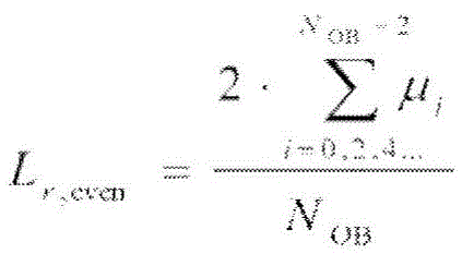
列偏移,其中NOB可以是每行OB像素的总数并且ui可以是OB像素i的中值(median),因此计算为:The column offset, where N OB can be the total number of OB pixels per row and ui can be the median of OB pixels i, is thus calculated as:

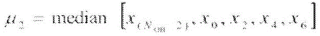
μ4=mcdian[x0,x2,x4,x6,x8]μ 4 =mcdian[x 0 , x 2 , x 4 , x 6 , x 8 ]
......

同样地,列偏移估计计数通道(确保两个ADC具有奇偶布置),行号r“Likewise, the column offset estimate counts channels (make sure both ADCs have parity arrangements), row number r"

其中:in:
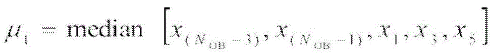
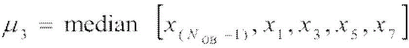
μ5=median[x1,x3,x5,x7,x9]μ 5 =median[x 1 , x 3 , x 5 , x 7 , x 9 ]
......

要获得总帧黑电平,一个好的实用方法可以通过累计所有列偏移以使用简单指数平滑法(SES)计算总黑电平而提供。使用SES的好处可以是:朝向帧的端部的行可以对最终黑估计具有较大影响,这对于发生在子帧时间尺度上黑偏移中的寻址变化可能是希望的。To obtain the total frame black level, a good practical method can be provided by accumulating all column offsets to calculate the total black level using Simple Exponential Smoothing (SES). The benefit of using SES may be that lines towards the end of the frame may have a larger influence on the final black estimate, which may be desirable for addressing changes that occur in black offsets on subframe time scales.
在SES中,每当抽样可用时,可以递增地调整节运行估计。为方便起见,在被添加至先前估计之前,抽样可以由二进制数(2q)分割。为了将结果标准化,先前估计可以可以每次首先与(2q-1)/2q相乘。q的高值导致稳定情况中一段时间较大的统计精确度。Q的较低值可以使得纠错对快速变化反应更大,q应当作为可调参数。In SES, the section running estimates can be adjusted incrementally whenever samples are available. For convenience, the samples may be divided by a binary number ( 2q ) before being added to the previous estimate. To normalize the results, the previous estimate may first be multiplied by ( 2q -1)/ 2q each time. High values of q result in greater statistical accuracy over time in the stable case. A lower value of Q can make the error correction more responsive to rapid changes, and q should be used as a tunable parameter.
kr=Lr(r=0)k r =L r (r=0)

其中,kr可以是行r之后的黑电平估计,并且Lr可以是对于每行r的列偏移估计。在阵列中的最后行已经增加之后,可以决定对黑钳位DAC做什么。where k r can be the black level estimate after row r and L r can be the column offset estimate for each row r. After the last row in the array has been added, a decision can be made about what to do with the black clamp DAC.
黑钳位算法将要求可以由可调整参数提供的目标黑电平。根据所观察到的黑色估计是否高于或者低于目标,所讨论的通道的传感器上的黑钳位DAC将被向上或者向下推送。只要黑电平可能靠近目标,推送的大小可以是例如的最小单位,即一个DAC计数。在黑钳位可能距离目标很远的情况下,可以作出较大比例的推送,参见图8A。该算法需要知道黑钳位DAC计数和传感器ADC计数之间对应关系的粗略校准和相对于输出黑电平的DAC调整的定向性。The black clamp algorithm will require a target black level that can be provided by an adjustable parameter. Depending on whether the observed black estimate is above or below the target, the black clamp DAC on the sensor of the channel in question will be pushed up or down. As long as the black level is likely to be close to the target, the size of the push can be, for example, the smallest unit, one DAC count. In situations where the black clamp may be very far from the target, a larger scale push can be made, see Figure 8A. The algorithm needs to know the rough calibration of the correspondence between the black clamp DAC counts and the sensor ADC counts and the directionality of the DAC adjustment relative to the output black level.
列噪声纠错中“列噪声”是指像素的水平行的偏移中随机的时间变化。可能存在多个源,但是其可以被看作是每当可以读出像素行时复位模拟元件导致的复位噪声。它可能是时间的并且应该对于每帧的每个新列计算新的纠错。由于在ADC输入处的放大级可能是最终的模拟元件,因此可以有很好的理由怀疑:列噪声可以现象学地显得每个ADC通道不独立。因此,最佳的做法可能是独立地纠正每个ADC(通道)。In column noise error correction, "column noise" refers to random temporal variations in the offset of horizontal rows of pixels. There may be multiple sources, but it can be seen as reset noise caused by resetting the analog elements each time a row of pixels can be read out. It may be temporal and a new error correction should be computed for each new column of each frame. Since the amplification stage at the ADC input may be the final analog component, there is good reason to suspect that column noise can phenomenologically appear to be independent of each ADC channel. Therefore, the best practice may be to correct each ADC (channel) independently.
由于用于列偏移估计的OB像素的抽样可以与被施加纠错的(并且抽样统计是有限的)抽样是分开的,因此完全消除列噪声也许是不可能的。假设所有的噪声可以是高斯的,纠错后的列噪声可以近似等于存在于OB像素中的像素时间噪声引起的列偏移估算中的不确定性。Since the sampling of OB pixels for column offset estimation may be separate from the sampling to which error correction is applied (and sampling statistics are limited), complete elimination of column noise may not be possible. Assuming that all noise can be Gaussian, the error-corrected column noise can be approximately equal to the uncertainty in the column offset estimation due to pixel temporal noise present in OB pixels.
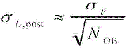
其中,σL,post可以是纠错后时间列噪声,σP可以是OB像素时间噪声并且NOB可以是OB像素的数量。列噪声纠错还引入空间列噪声分量,主要由于存在于OB像素内的像素FPN:where σL ,post can be post-error correction temporal column noise, σP can be OB pixel temporal noise and NO OB can be the number of OB pixels. Column noise error correction also introduces a spatial column noise component, mainly due to the pixel FPN that exists within the OB pixel:
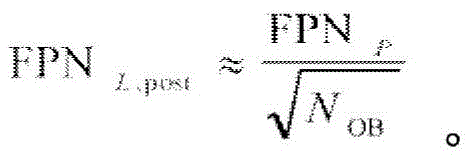
伪影可以后续在链中由FPN纠错消除。模拟已经指示:为了使时间列噪声不可见,幅度应该小于像素时间噪声的约1/10。该纠错指示每行需要100OB像素。Artifacts can be removed later in the chain by FPN error correction. Simulations have indicated that in order to make temporal column noise invisible, the magnitude should be less than about 1/10 of the pixel temporal noise. This error correction indicates that 100OB pixels are required per line.
列噪声纠错应用至光学观测(清楚的)像素:Column noise error correction applied to optically observed (clear) pixels:
x′i=xi-L+Bx′ i = xi -L+B
其中L可以是对于当前列的列偏移估计,从“黑钳位”模块传输并且B可以是黑钳位目标电平。where L may be the column offset estimate for the current column, transmitted from the "black clamp" module and B may be the black clamp target level.
完整列重组。这将涉及简单组合两个数据通道成为完整列。它们需要被交错为使得最终清楚像素顺序反映阵列中的正确顺序。Complete column reorganization. This would involve simply combining the two data channels into a full column. They need to be interleaved so that it is ultimately clear that the pixel order reflects the correct order in the array.
FPN纠错,CMOS图像传感器具有多个噪声源,噪声源的幅度和外观取决于物理条件的范围。没有相干分量的纯泊松或高斯时间噪声(例如光子散粒噪声或者源极跟随器1/f读噪声)看起来像噪声可以看起来一样自然。所有的其它可感知的噪声类型可以对于相同的幅度降低图像质量至更大的程度。空间噪声(FPN)可能是特别令人震惊并且CMOS传感器固有地具有至少两个源;像素FPN和列FPN。像素FPN可能主要是由于来自逐个像素(DSNU)的光电二极管漏电流(暗信号)中的变化。这个源可以是以指数方式依赖于结温(7)和并且线性地依赖于曝光时间。列FPN可以是读出结构的结果,读出结构中相同列内的像素通过公共模拟读出元件被引导。FPN error correction, CMOS image sensors have multiple noise sources, the magnitude and appearance of the noise sources depend on a range of physical conditions. Pure Poisson or Gaussian temporal noise with no coherent components (eg photon shot noise or source follower 1/f read noise) looks as natural as noise can look. All other perceived noise types can degrade image quality to a greater extent for the same magnitude. Spatial noise (FPN) can be particularly alarming and CMOS sensors inherently have at least two sources; pixel FPN and column FPN. Pixel FPN may be primarily due to variations in photodiode leakage current (dark signal) from pixel by pixel (DSNU). This source can be exponentially dependent on junction temperature (7) and linearly dependent on exposure time. Column FPN may be the result of a readout structure in which pixels within the same column are directed through a common analog readout element.
通常,片上数字FPN纠错将涉及仅处理列FPN分量,需求每列一个偏移纠错寄存器。这样纠错的精确度可能通常是每列20比特左右,其转换成用于1920X 1080阵列约为5kB的RAM。迁移数字传感器纠错至ISP的一个好处可以是RAM的随时可用。这开创了取消任何行、列或者逐像素组件的全面FPN纠错的可能性。这可以通过简单指数平滑法(SES)而实现,指数平滑法中每个新的黑帧抽样可以用于调节每个物理像素基础上的运行偏移估计。Typically, on-chip digital FPN error correction will involve processing column FPN components only, requiring one offset error correction register per column. The accuracy of such error correction may typically be around 20 bits per column, which translates to about 5kB of RAM for a 1920X 1080 array. One benefit of migrating digital sensor error correction to an ISP can be the ready availability of RAM. This opens up the possibility to cancel any row, column or pixel-by-pixel component of full FPN error correction. This can be achieved by Simple Exponential Smoothing (SES), where each new black frame sample can be used to adjust the running offset estimate on a per physical pixel basis.
可编程数字增益。图6中的最后一块对应于可编程数字放大器。CMOS iSoC通常装配具有非常精细的增量的数字可编程增益级。这可能是有助于自动曝光过程,其通常调节增益和曝光时间。Programmable digital gain. The last block in Figure 6 corresponds to a programmable digital amplifier. CMOS iSoCs typically feature digitally programmable gain stages with very fine increments. This may be helpful for the automatic exposure process, which normally adjusts gain and exposure time.
数字放大器可以用于将传感器ADC的范围与ISP(例如,对于11比特ADC×2至12比特ISP)的范围对齐。少量的数字增益也可以被用于修剪数字列噪声的印记和FPN纠错,其在ADC的全部范围变得明显。A digital amplifier can be used to align the range of the sensor ADC with the range of the ISP (eg, for an 11-bit ADC x 2 to 12-bit ISP). A small amount of digital gain can also be used to trim the imprint of the digital column noise and FPN error correction, which becomes apparent over the full range of the ADC.
配置寄存器地址ROM的最小化。传统CMOS图像传感器包括用于控制传感器如何操作的许多可写寄存器。它们将通常包括DAC设置以调节偏置电压和电流、定时参数,以例如用于像素获取和读出周期,放大器偏移和增益等。通常的惯例可以分配一个特定的8比特或16比特的地址给通常包括8或者16比特数据的每个寄存器。Minimization of configuration register address ROM. Traditional CMOS image sensors include many writable registers for controlling how the sensor operates. They will typically include DAC settings to adjust bias voltage and current, timing parameters for eg pixel acquisition and readout cycles, amplifier offset and gain, etc. It is common practice to assign a specific 8-bit or 16-bit address to each register that typically contains 8 or 16 bits of data.
一个更节省空间的方法涉及组合大量的控制RAM成为单个、长寄存器。在极端情况下,所有参数可以被放置进单个寄存器,不需要地址ROM。然而由于写控制寄存器需要时间并且典型的视频应用涉及基于逐帧改变少量操作参数(例如曝光时间),因此这种解决方案可能不是很实际的。最实际的解决方案可以通过功能地连接相关的参数集合成为少量长寄存器来提供。具有比如10个寄存器(需要4个地址比特)相对一个寄存器而言的空间上的差异可以忽略不计。具体而言,以高速率(例如每帧)周期性地写入的所有参数一切属于唯一的寄存器(帧寄存器)是有意义的。这些参数包括曝光时间、收益、增量偏移调整和维持连续高品质视频所需的任何其它。如果如前面所描述地数字数据通路逻辑已经被迁移出芯片,则黑钳位电压调节数据也属于该寄存器,因此它也应该每帧都被修正。在实现中,在该配置阶段期间,寄存器可以被写入并且进而相对于总帧定时的帧寄存器写入的定时应当由相机仔细控制。A more space-efficient approach involves combining large amounts of control RAM into a single, long register. In extreme cases, all parameters can be placed into a single register, no address ROM is required. However, this solution may not be very practical since writing control registers takes time and typical video applications involve changing a small number of operating parameters (eg exposure time) on a frame-by-frame basis. The most practical solution can be provided by functionally concatenating sets of related parameters into a small number of long registers. With eg 10 registers (requiring 4 address bits) the difference in space versus one register is negligible. In particular, it makes sense that all parameters written periodically at a high rate (eg every frame) belong to a unique register (frame register). These parameters include exposure time, gain, incremental offset adjustments and anything else needed to maintain continuous high quality video. If the digital datapath logic has been migrated off-chip as previously described, the black clamp voltage adjustment data also belongs to this register, so it should also be revised every frame. In an implementation, during this configuration phase, the registers can be written and thus the timing of frame register writes relative to the overall frame timing should be carefully controlled by the camera.
参数寄存器分组的其它实例可以包括模拟电流、模拟电压、像素定时、垂直定时、传感器命令(复位等)等。在图9中,寄存器的布置可以示出为具体最小面积传感器设计。“命令”寄存器可用于最高级别面向事件的1比特命令,例如芯片复位和其它寄存器下方示出的对于其它寄存器的负载。2线协议地址译码器决定哪些移位寄存器直接输入2线协议数据。为了下载“格式”寄存器,例如外部控制器发送具有与格式寄存器关联的地址的命令。这放置数据流进入格式寄存器移位寄存器。然后为了锁存数据,跟踪命令被发送至设置有特定“负载格式”比特的命令寄存器。可以理解的是,可以使用多个控制寄存器。控制寄存器可以是数字锁存器,其经由移位寄存器被加载。移位寄存器可以是任意长度的。在一个实施例中,多个控制寄存器中的大部分可以使用包括数十比特的移位寄存器被加载。在一个实施例中,移位寄存器可以使用串行的、2线协议而被加载。在一个实施例中,移位寄存器中的一个可以专用于帧到帧参数变化诸如,例如,积分时间和黑钳位偏移调整。Other examples of parameter register groups may include analog current, analog voltage, pixel timing, vertical timing, sensor commands (reset, etc.), and the like. In Figure 9, the arrangement of registers can be shown for a specific minimum area sensor design. The "Command" register is available for highest level event-oriented 1-bit commands, such as chip resets and loads for other registers shown below other registers. The 2-wire protocol address decoder determines which shift registers directly input 2-wire protocol data. To download the "format" register, for example, the external controller sends a command with the address associated with the format register. This places the data stream into the format register shift register. Then in order to latch the data, the trace command is sent to the command register set with certain "payload format" bits. It will be appreciated that multiple control registers may be used. The control register may be a digital latch, which is loaded via a shift register. Shift registers can be of any length. In one embodiment, most of the plurality of control registers may be loaded using shift registers comprising tens of bits. In one embodiment, the shift register may be loaded using a serial, 2-wire protocol. In one embodiment, one of the shift registers may be dedicated to frame-to-frame parameter changes such as, for example, integration time and black clamp offset adjustment.
图10示出了用于内窥镜应用的最小面积传感器的实施例的整体框图,其中传感器可以包括入内窥镜单元的远端。Figure 10 shows an overall block diagram of an embodiment of a minimum area sensor for endoscopic applications, where the sensor may include the distal end of the endoscopic unit.
图11A和图11B分别示出了根据本公开的教导和原理具有用于生成三维图像的多个像素阵列的单片式传感器2900的实现的立体图和侧视图。这样的实现对于三维图像获取是希望的,其中两个像素阵列2902和2904可以在使用过程中被抵消。在另一个实现中,第一像素阵列2902和第二像素阵列2904可以是专用于接收电磁辐射的波长的预定范围,其中第一像素阵列专用于与第二像素阵列不同的电磁辐射的波长范围。FIGS. 11A and 11B illustrate perspective and side views, respectively, of an implementation of a
图12A和图12B分别示出建立在多个基板上的成像传感器3000的实现的立体图和侧视图。如图所示,形成像素阵列的多个像素列3004位于第一基板3002上并且多个电路列3008位于第二基板3006上。还在图中示出的是一列像素至其关联或者对应的列的电路的电连接和电通信。在一个实现中,或者可以是利用其像素阵列制造的并且支撑单个、单片式基板/芯片上电路的成像传感器可以具有与所有或者大部分支撑电路分开的像素阵列。本公开可使用利用三维堆叠技术被堆叠在一起的至少两个基板/芯片。两个基板/芯片的第一基板/芯片3002可以使用图像CMOS方法进行处理。第一基板/芯片3002可以包括专有的像素阵列或者由有限的电路包围的像素阵列。第二或者随后的基板/芯片3006可以使用任何方法进行处理,并且不必是来自图像CMOS方法。为了在或者基板/芯片上十分有限的空间或者面积中集成多种和多个功能,或者混合模式或者模拟方法,为了集成例如精确的模拟功能或者RF方法,为了实现无线功能或者MEMS(微机电系统),为了集成MEMS设备,第二基板/芯片3006可以是但是不限于高密度的数字处理。可以使用任何三维技术,将图像CMOS基板/芯片3002与第二或者后续基板/芯片3006堆叠。第二基板/芯片3006可以支持大多或者大部分电路,其否则将在第一图像CMOS芯片3002(如果在单片基板/芯片上实现)中实现为外围电路并且进而增加了整个系统的面积同时保持像素阵列的尺寸不变,并且因此在最大可能程度说被优化。两个基板/芯片之间的电连接可以通过3003和3005的互连实现,其可以是线接合,碰撞和/或TSV(硅穿孔)。12A and 12B illustrate perspective and side views, respectively, of an implementation of an
图13A和13B分别示出了用于生成三维图像的多个像素阵列的传感器3100的实现的立体图和侧视图。三维成像传感器可以被构建在多个基板上并且可以包括多个像素阵列和其它关联电路,其中形成第一像素阵列的多个像素列3104a和形成第二像素阵列的多个像素列3104b分别位于相应的3102a和3102b,并且多个电路列3108a和3108b都位于分开基板3106上。还示出的是像素列至关联或者电路对应列之间的电连接和通信。Figures 13A and 13B show perspective and side views, respectively, of an implementation of a
可以理解的是,本公开的教导和原理可以在可重复使用设备平台、有限使用设备平台、重新仿真(re-posable)使用设备平台或者单次使用/一次性设备平台中使用,而不偏离本公开的范围。可以理解的是,在可重复使用设备平台中,最终用户负责设备的清洁和灭菌。在有限使用设备平台中,在变得不可操作前设备可以被使用一些特定的次数。典型的新设备利用需要最终用户在附加用途之前清洁和灭菌的附加用途无菌交付。在重新仿真(re-posable)使用设备平台中,第三方可以重新处理设备(例如,清洁、打包和灭菌),用于附加用途的单次使用设备以比新单元更低的成本使用。在单次使用/一次性设备平台中,设备提供对操作室的灭菌并且在被布置前仅能使用一次。It will be appreciated that the teachings and principles of the present disclosure may be used in reusable device platforms, limited use device platforms, re-posable use device platforms, or single-use/disposable device platforms without departing from the present disclosure. public scope. Understandably, in a reusable device platform, the end user is responsible for cleaning and sterilizing the device. In a limited use device platform, a device can be used a certain number of times before becoming inoperable. Typical new equipment utilizes aseptic delivery for additional use that requires the end user to clean and sterilize prior to additional use. In a re-posable use device platform, third parties can reprocess the device (eg, clean, package, and sterilize), and single-use devices for additional uses can be used at a lower cost than new units. In a single use/disposable device platform, the device provides sterilization of the operating chamber and can only be used once before being deployed.
在封闭光环境中使用的内窥镜的实施例可以包括:内窥镜主体,其提供手持结构;内腔,其由主体第一端处的内腔基座附接;内腔的尖端部,其与内腔基座相对;透镜,其可以设置在尖端部的最远端部;成像传感器,其可以靠近内腔的尖端部设置,包括用于感测电磁辐射的像素阵列,其中,像素阵列可以具有有源像素和光学黑色像素以用于纠错来自所述像素阵列的输出;其中光学黑色像素可被组织在与像素阵列内有源像素邻近的列中;传递端口,其用于传递由像素阵列生成的数据;数字转换器,其转换模拟像素抽样成数字数值;黑钳位电路,其提供对由像素阵列生成的数据的偏移控制;可以存储在用于控制黑钳位电路的存储器内的过程;电连接,其可以提供成像传感器和图像信号处理电路之间的电通信,图像信号处理电路可以远离内窥镜主体和控制单元内的成像传感器设置。Embodiments of endoscopes for use in closed light environments may include: an endoscope body that provides a hand-held structure; a lumen attached by a lumen base at a first end of the body; a tip portion of the lumen, Opposite the lumen base; a lens, which may be disposed at the most distal end of the tip; an imaging sensor, which may be disposed near the tip of the lumen, including an array of pixels for sensing electromagnetic radiation, wherein the array of pixels There may be active pixels and optical black pixels for error correction of the output from the pixel array; wherein the optical black pixels may be organized in columns adjacent to active pixels within the pixel array; a pass port for passing the Data generated by the pixel array; a digitizer that converts analog pixel samples into digital values; a black clamp circuit that provides offset control of the data generated by the pixel array; may be stored in memory for controlling the black clamp circuit process within; electrical connections that can provide electrical communication between the imaging sensor and an image signal processing circuit that can be located remotely from the endoscope body and the imaging sensor within the control unit.
环境光线不足的环境中用于数字成像的系统实施例可以包括:成像传感器,其用于感测电磁辐射,其中所述成像传感器可进一步包括:像素阵列,其具有有源像素及光学黑色像素以纠错来自所述像素阵列的输出;其中光学黑色像素可被组织在与像素阵列内有源像素邻近的列中;传递端口,其用于传递由像素阵列生成的数据;数字转换器,其转换模拟像素抽样成数字数值;黑钳位电路,其提供对由像素阵列生成的数据的偏移控制;可以存储在用于控制黑钳位电路的系统的存储器内的过程;内窥镜,其用于接近环境光线不足的环境;手持件,其附接至所述内窥镜并且其中所述内窥镜可以由操作手持件而操作;控制单元,其包括处理器并且其中所述控制单元可以与成像传感器电通信;以及电连接手持件和控制单元的连接线缆。Embodiments of the system for digital imaging in low ambient light environments may include an imaging sensor for sensing electromagnetic radiation, wherein the imaging sensor may further include a pixel array having active pixels and optical black pixels to Error correction from the output of the pixel array; wherein optical black pixels may be organized in columns adjacent to active pixels within the pixel array; a pass-through port for passing data generated by the pixel array; a digitizer, which converts Analog pixels are sampled into digital values; black clamp circuits, which provide offset control of data generated by pixel arrays; procedures that can be stored in the memory of a system for controlling black clamp circuits; endoscopes, which use a handpiece that is attached to the endoscope and wherein the endoscope can be operated by operating the handpiece; a control unit that includes a processor and wherein the control unit can interact with The imaging sensor is in electrical communication; and a connecting cable electrically connects the handpiece and the control unit.
此外,本公开的教导和原理可以包括电磁能的任何和所有的波长,其包括可见光和非可见光光谱,例如红外(IR)、紫外线(UV)和X射线。Furthermore, the teachings and principles of the present disclosure may encompass any and all wavelengths of electromagnetic energy, including the visible and non-visible light spectrum, such as infrared (IR), ultraviolet (UV), and X-rays.
前面的描述是为了说明和描述的目的而展示。其并不旨在详尽地或限制本公开至精确形式的公开。许多修改和变化根据上述教导是可能的。此外,应该指出的是,前述替换实施的任何或者全部可以用于所希望的任何组合以形成本公开的其它混合实施。The foregoing description has been presented for purposes of illustration and description. It is not intended to be exhaustive or to limit the disclosure to its precise form. Many modifications and variations are possible in light of the above teachings. Furthermore, it should be noted that any or all of the foregoing alternative implementations may be used in any combination desired to form other hybrid implementations of the present disclosure.
此外,尽管本公开的具体实施已经描述和示出,但是本公开并不限制至所描述和示出的部件的具体形式或者布置。本公开的范围可以由此处所附上的权利要求、此处和不同申请中递交的任何其它权利要求及其等同物而限定。Furthermore, although specific implementations of the present disclosure have been described and illustrated, the disclosure is not to be limited to the specific forms or arrangements of components described and illustrated. The scope of the disclosure may be defined by the claims appended hereto, any other claims filed herein and in a different application, and their equivalents.
Claims (71)
Applications Claiming Priority (5)
| Application Number | Priority Date | Filing Date | Title |
|---|---|---|---|
| US201261676289P | 2012-07-26 | 2012-07-26 | |
| US61/676289 | 2012-07-26 | ||
| US201361790590P | 2013-03-15 | 2013-03-15 | |
| US61/790590 | 2013-03-15 | ||
| CN201380038876.9A CN104486987A (en) | 2012-07-26 | 2013-07-26 | Camera system with smallest area monolithic CMOS image sensor |
Related Parent Applications (1)
| Application Number | Title | Priority Date | Filing Date |
|---|---|---|---|
| CN201380038876.9A Division CN104486987A (en) | 2012-07-26 | 2013-07-26 | Camera system with smallest area monolithic CMOS image sensor |
Publications (1)
| Publication Number | Publication Date |
|---|---|
| CN111938543A true CN111938543A (en) | 2020-11-17 |
Family
ID=49997991
Family Applications (2)
| Application Number | Title | Priority Date | Filing Date |
|---|---|---|---|
| CN202010638131.8A Pending CN111938543A (en) | 2012-07-26 | 2013-07-26 | Camera system with minimum area monolithic CMOS image sensor |
| CN201380038876.9A Pending CN104486987A (en) | 2012-07-26 | 2013-07-26 | Camera system with smallest area monolithic CMOS image sensor |
Family Applications After (1)
| Application Number | Title | Priority Date | Filing Date |
|---|---|---|---|
| CN201380038876.9A Pending CN104486987A (en) | 2012-07-26 | 2013-07-26 | Camera system with smallest area monolithic CMOS image sensor |
Country Status (13)
| Country | Link |
|---|---|
| US (5) | US9462234B2 (en) |
| EP (1) | EP2877079B1 (en) |
| JP (1) | JP6461790B2 (en) |
| KR (1) | KR102143807B1 (en) |
| CN (2) | CN111938543A (en) |
| AU (1) | AU2013295565B2 (en) |
| BR (1) | BR112015001369A2 (en) |
| CA (1) | CA2878512A1 (en) |
| HK (1) | HK1207550A1 (en) |
| IL (1) | IL236894B (en) |
| IN (1) | IN2015MN00019A (en) |
| MX (1) | MX344146B (en) |
| WO (1) | WO2014018948A2 (en) |
Families Citing this family (113)
| Publication number | Priority date | Publication date | Assignee | Title |
|---|---|---|---|---|
| US20070167681A1 (en) | 2001-10-19 | 2007-07-19 | Gill Thomas J | Portable imaging system employing a miniature endoscope |
| CN103648378B (en) | 2011-05-12 | 2016-10-12 | 橄榄医疗公司 | For using the system and method for the vertically sub-row parallel digitizers of the hybrid stack-ups imageing sensor of interconnection |
| CN111938543A (en) | 2012-07-26 | 2020-11-17 | 德普伊辛迪斯制品公司 | Camera system with minimum area monolithic CMOS image sensor |
| US8786732B2 (en) | 2012-10-31 | 2014-07-22 | Pixon Imaging, Inc. | Device and method for extending dynamic range in an image sensor |
| CA2906953A1 (en) | 2013-03-15 | 2014-09-18 | Olive Medical Corporation | Image sensor synchronization without input clock and data transmission clock |
| AU2014233192B2 (en) | 2013-03-15 | 2018-11-22 | DePuy Synthes Products, Inc. | Minimize image sensor I/O and conductor counts in endoscope applications |
| FR3020735B1 (en) * | 2014-04-30 | 2017-09-15 | Ulis | METHOD FOR PROCESSING AN INFRARED IMAGE FOR NON-UNIFORMITY CORRECTION |
| US9615013B2 (en) | 2014-12-22 | 2017-04-04 | Google Inc. | Image sensor having multiple output ports |
| US9918073B2 (en) | 2014-12-22 | 2018-03-13 | Google Llc | Integrated camera system having two dimensional image capture and three dimensional time-of-flight capture with movable illuminated region of interest |
| WO2016185700A1 (en) * | 2015-05-21 | 2016-11-24 | 富士フイルム株式会社 | Infrared imaging device and signal correction method using infrared imaging device |
| WO2016185698A1 (en) * | 2015-05-21 | 2016-11-24 | 富士フイルム株式会社 | Infrared imaging device |
| WO2016185699A1 (en) * | 2015-05-21 | 2016-11-24 | 富士フイルム株式会社 | Infrared imaging device |
| WO2016185697A1 (en) * | 2015-05-21 | 2016-11-24 | 富士フイルム株式会社 | Infrared imaging device and signal correction method using infrared imaging device |
| US12150636B2 (en) | 2015-09-04 | 2024-11-26 | Medos International Sárl | Surgical instrument connectors and related methods |
| CN113143355A (en) | 2015-09-04 | 2021-07-23 | 美多斯国际有限公司 | Multi-shield spinal access system |
| US11439380B2 (en) | 2015-09-04 | 2022-09-13 | Medos International Sarl | Surgical instrument connectors and related methods |
| US11744447B2 (en) | 2015-09-04 | 2023-09-05 | Medos International | Surgical visualization systems and related methods |
| US10987129B2 (en) | 2015-09-04 | 2021-04-27 | Medos International Sarl | Multi-shield spinal access system |
| US11672562B2 (en) | 2015-09-04 | 2023-06-13 | Medos International Sarl | Multi-shield spinal access system |
| CN108140649B (en) * | 2015-10-01 | 2022-05-06 | 奥林巴斯株式会社 | Camera elements, endoscopes and endoscope systems |
| GB2548341A (en) * | 2016-03-10 | 2017-09-20 | Moog Bv | Movement tracking and simulation device and method |
| JP6677594B2 (en) * | 2016-06-30 | 2020-04-08 | キヤノン株式会社 | Photoelectric conversion device |
| TWI635257B (en) * | 2016-12-02 | 2018-09-11 | 矽統科技股份有限公司 | Sensing device |
| JP6724173B2 (en) * | 2017-02-01 | 2020-07-15 | 富士フイルム株式会社 | Endoscope system and operating method thereof |
| US20180228361A1 (en) * | 2017-02-15 | 2018-08-16 | Dynacolor, Inc. | Arthroscopic system with disposable arthroscope |
| US11109747B2 (en) * | 2017-02-15 | 2021-09-07 | Dynacolor, Inc. | Arthroscopic system with disposable arthroscope having image rotation function and method thereof |
| WO2018156668A1 (en) * | 2017-02-22 | 2018-08-30 | Flir Systems, Inc. | Low cost and high performance bolometer circuitry and methods |
| WO2018180339A1 (en) * | 2017-03-30 | 2018-10-04 | Hoya株式会社 | Electronic endoscope device |
| CN107222591B (en) * | 2017-05-03 | 2021-02-05 | Oppo广东移动通信有限公司 | Image sensor, camera module and electronic device |
| CN110650669B (en) * | 2017-05-19 | 2021-07-13 | 奥林巴斯株式会社 | camera |
| EP3471086B1 (en) * | 2017-08-16 | 2020-06-10 | Shenzhen Goodix Technology Co., Ltd. | Image sensing circuit and image depth sensing system |
| JP7258900B2 (en) | 2018-02-21 | 2023-04-17 | メドス・インターナショナル・エスエイアールエル | Surgical visualization system and related methods |
| US11288772B2 (en) | 2019-06-20 | 2022-03-29 | Cilag Gmbh International | Super resolution and color motion artifact correction in a pulsed fluorescence imaging system |
| US11412920B2 (en) | 2019-06-20 | 2022-08-16 | Cilag Gmbh International | Speckle removal in a pulsed fluorescence imaging system |
| US11898909B2 (en) | 2019-06-20 | 2024-02-13 | Cilag Gmbh International | Noise aware edge enhancement in a pulsed fluorescence imaging system |
| US11280737B2 (en) | 2019-06-20 | 2022-03-22 | Cilag Gmbh International | Super resolution and color motion artifact correction in a pulsed fluorescence imaging system |
| US11389066B2 (en) | 2019-06-20 | 2022-07-19 | Cilag Gmbh International | Noise aware edge enhancement in a pulsed hyperspectral, fluorescence, and laser mapping imaging system |
| US11252326B2 (en) | 2019-06-20 | 2022-02-15 | Cilag Gmbh International | Pulsed illumination in a laser mapping imaging system |
| US11172810B2 (en) | 2019-06-20 | 2021-11-16 | Cilag Gmbh International | Speckle removal in a pulsed laser mapping imaging system |
| US11931009B2 (en) | 2019-06-20 | 2024-03-19 | Cilag Gmbh International | Offset illumination of a scene using multiple emitters in a hyperspectral imaging system |
| US11237270B2 (en) | 2019-06-20 | 2022-02-01 | Cilag Gmbh International | Hyperspectral, fluorescence, and laser mapping imaging with fixed pattern noise cancellation |
| US11758256B2 (en) | 2019-06-20 | 2023-09-12 | Cilag Gmbh International | Fluorescence imaging in a light deficient environment |
| US11213194B2 (en) | 2019-06-20 | 2022-01-04 | Cilag Gmbh International | Optical fiber waveguide in an endoscopic system for hyperspectral, fluorescence, and laser mapping imaging |
| US11134832B2 (en) | 2019-06-20 | 2021-10-05 | Cilag Gmbh International | Image rotation in an endoscopic hyperspectral, fluorescence, and laser mapping imaging system |
| US11233960B2 (en) | 2019-06-20 | 2022-01-25 | Cilag Gmbh International | Fluorescence imaging with fixed pattern noise cancellation |
| US12440085B2 (en) | 2019-06-20 | 2025-10-14 | Cilag Gmbh International | Image synchronization without input clock and data transmission clock in a pulsed laser mapping imaging system |
| US10979646B2 (en) * | 2019-06-20 | 2021-04-13 | Ethicon Llc | Fluorescence imaging with minimal area monolithic image sensor |
| US11311183B2 (en) | 2019-06-20 | 2022-04-26 | Cilag Gmbh International | Controlling integral energy of a laser pulse in a fluorescence imaging system |
| US11276148B2 (en) | 2019-06-20 | 2022-03-15 | Cilag Gmbh International | Super resolution and color motion artifact correction in a pulsed fluorescence imaging system |
| US11172811B2 (en) | 2019-06-20 | 2021-11-16 | Cilag Gmbh International | Image rotation in an endoscopic fluorescence imaging system |
| US11531112B2 (en) | 2019-06-20 | 2022-12-20 | Cilag Gmbh International | Offset illumination of a scene using multiple emitters in a hyperspectral, fluorescence, and laser mapping imaging system |
| US11633089B2 (en) | 2019-06-20 | 2023-04-25 | Cilag Gmbh International | Fluorescence imaging with minimal area monolithic image sensor |
| US10841504B1 (en) * | 2019-06-20 | 2020-11-17 | Ethicon Llc | Fluorescence imaging with minimal area monolithic image sensor |
| US11716543B2 (en) | 2019-06-20 | 2023-08-01 | Cilag Gmbh International | Wide dynamic range using a monochrome image sensor for fluorescence imaging |
| US11624830B2 (en) | 2019-06-20 | 2023-04-11 | Cilag Gmbh International | Wide dynamic range using a monochrome image sensor for laser mapping imaging |
| US11516387B2 (en) | 2019-06-20 | 2022-11-29 | Cilag Gmbh International | Image synchronization without input clock and data transmission clock in a pulsed hyperspectral, fluorescence, and laser mapping imaging system |
| US11412152B2 (en) | 2019-06-20 | 2022-08-09 | Cilag Gmbh International | Speckle removal in a pulsed hyperspectral imaging system |
| US11375886B2 (en) | 2019-06-20 | 2022-07-05 | Cilag Gmbh International | Optical fiber waveguide in an endoscopic system for laser mapping imaging |
| US11793399B2 (en) | 2019-06-20 | 2023-10-24 | Cilag Gmbh International | Super resolution and color motion artifact correction in a pulsed hyperspectral imaging system |
| US11221414B2 (en) | 2019-06-20 | 2022-01-11 | Cilag Gmbh International | Laser mapping imaging with fixed pattern noise cancellation |
| US11788963B2 (en) | 2019-06-20 | 2023-10-17 | Cilag Gmbh International | Minimizing image sensor input/output in a pulsed fluorescence imaging system |
| US11187658B2 (en) | 2019-06-20 | 2021-11-30 | Cilag Gmbh International | Fluorescence imaging with fixed pattern noise cancellation |
| US11294062B2 (en) | 2019-06-20 | 2022-04-05 | Cilag Gmbh International | Dynamic range using a monochrome image sensor for hyperspectral and fluorescence imaging and topology laser mapping |
| US11671691B2 (en) | 2019-06-20 | 2023-06-06 | Cilag Gmbh International | Image rotation in an endoscopic laser mapping imaging system |
| US11986160B2 (en) * | 2019-06-20 | 2024-05-21 | Cllag GmbH International | Image synchronization without input clock and data transmission clock in a pulsed hyperspectral imaging system |
| US11012599B2 (en) | 2019-06-20 | 2021-05-18 | Ethicon Llc | Hyperspectral imaging in a light deficient environment |
| US11218645B2 (en) | 2019-06-20 | 2022-01-04 | Cilag Gmbh International | Wide dynamic range using a monochrome image sensor for fluorescence imaging |
| US11937784B2 (en) | 2019-06-20 | 2024-03-26 | Cilag Gmbh International | Fluorescence imaging in a light deficient environment |
| US11533417B2 (en) | 2019-06-20 | 2022-12-20 | Cilag Gmbh International | Laser scanning and tool tracking imaging in a light deficient environment |
| US11550057B2 (en) | 2019-06-20 | 2023-01-10 | Cilag Gmbh International | Offset illumination of a scene using multiple emitters in a fluorescence imaging system |
| US11471055B2 (en) | 2019-06-20 | 2022-10-18 | Cilag Gmbh International | Noise aware edge enhancement in a pulsed fluorescence imaging system |
| US11540696B2 (en) | 2019-06-20 | 2023-01-03 | Cilag Gmbh International | Noise aware edge enhancement in a pulsed fluorescence imaging system |
| US11265491B2 (en) | 2019-06-20 | 2022-03-01 | Cilag Gmbh International | Fluorescence imaging with fixed pattern noise cancellation |
| US11895397B2 (en) | 2019-06-20 | 2024-02-06 | Cilag Gmbh International | Image synchronization without input clock and data transmission clock in a pulsed fluorescence imaging system |
| US11147436B2 (en) | 2019-06-20 | 2021-10-19 | Cilag Gmbh International | Image rotation in an endoscopic fluorescence imaging system |
| US12013496B2 (en) | 2019-06-20 | 2024-06-18 | Cilag Gmbh International | Noise aware edge enhancement in a pulsed laser mapping imaging system |
| US11122967B2 (en) | 2019-06-20 | 2021-09-21 | Cilag Gmbh International | Driving light emissions according to a jitter specification in a fluorescence imaging system |
| US11622094B2 (en) | 2019-06-20 | 2023-04-04 | Cilag Gmbh International | Wide dynamic range using a monochrome image sensor for fluorescence imaging |
| US11457154B2 (en) | 2019-06-20 | 2022-09-27 | Cilag Gmbh International | Speckle removal in a pulsed hyperspectral, fluorescence, and laser mapping imaging system |
| US10952619B2 (en) * | 2019-06-20 | 2021-03-23 | Ethicon Llc | Hyperspectral and fluorescence imaging and topology laser mapping with minimal area monolithic image sensor |
| US11700995B2 (en) | 2019-06-20 | 2023-07-18 | Cilag Gmbh International | Speckle removal in a pulsed fluorescence imaging system |
| US11187657B2 (en) | 2019-06-20 | 2021-11-30 | Cilag Gmbh International | Hyperspectral imaging with fixed pattern noise cancellation |
| US11122968B2 (en) | 2019-06-20 | 2021-09-21 | Cilag Gmbh International | Optical fiber waveguide in an endoscopic system for hyperspectral imaging |
| US11712155B2 (en) | 2019-06-20 | 2023-08-01 | Cilag GmbH Intenational | Fluorescence videostroboscopy of vocal cords |
| US11398011B2 (en) | 2019-06-20 | 2022-07-26 | Cilag Gmbh International | Super resolution and color motion artifact correction in a pulsed laser mapping imaging system |
| US11903563B2 (en) | 2019-06-20 | 2024-02-20 | Cilag Gmbh International | Offset illumination of a scene using multiple emitters in a fluorescence imaging system |
| US11674848B2 (en) | 2019-06-20 | 2023-06-13 | Cilag Gmbh International | Wide dynamic range using a monochrome image sensor for hyperspectral imaging |
| US11892403B2 (en) | 2019-06-20 | 2024-02-06 | Cilag Gmbh International | Image synchronization without input clock and data transmission clock in a pulsed fluorescence imaging system |
| US20200397240A1 (en) * | 2019-06-20 | 2020-12-24 | Ethicon Llc | Laser mapping with minimal area monolithic image sensor |
| US11925328B2 (en) | 2019-06-20 | 2024-03-12 | Cilag Gmbh International | Noise aware edge enhancement in a pulsed hyperspectral imaging system |
| US11432706B2 (en) * | 2019-06-20 | 2022-09-06 | Cilag Gmbh International | Hyperspectral imaging with minimal area monolithic image sensor |
| US12126887B2 (en) | 2019-06-20 | 2024-10-22 | Cilag Gmbh International | Hyperspectral and fluorescence imaging with topology laser scanning in a light deficient environment |
| EP4030983B1 (en) * | 2019-12-03 | 2025-08-13 | Boston Scientific Scimed, Inc. | Medical system comprising a medical imaging device with a light source and means to move a sensor based on the detection of light by the sensor |
| JP2022018705A (en) * | 2020-07-16 | 2022-01-27 | キヤノン株式会社 | Semiconductor device |
| US12064293B2 (en) | 2020-10-02 | 2024-08-20 | Cilag Gmbh International | Field programmable surgical visualization system |
| US12484897B2 (en) | 2020-10-02 | 2025-12-02 | Cilag Gmbh International | Surgical instrument with adaptive configuration control |
| US12213801B2 (en) | 2020-10-02 | 2025-02-04 | Cilag Gmbh International | Surgical visualization and particle trend analysis system |
| US12016566B2 (en) | 2020-10-02 | 2024-06-25 | Cilag Gmbh International | Surgical instrument with adaptive function controls |
| US11877897B2 (en) | 2020-10-02 | 2024-01-23 | Cilag Gmbh International | Situational awareness of instruments location and individualization of users to control displays |
| US11748924B2 (en) | 2020-10-02 | 2023-09-05 | Cilag Gmbh International | Tiered system display control based on capacity and user operation |
| US11830602B2 (en) | 2020-10-02 | 2023-11-28 | Cilag Gmbh International | Surgical hub having variable interconnectivity capabilities |
| US12472032B2 (en) | 2020-10-02 | 2025-11-18 | Cilag Gmbh International | Monitoring of user visual gaze to control which display system displays the primary information |
| US11672534B2 (en) | 2020-10-02 | 2023-06-13 | Cilag Gmbh International | Communication capability of a smart stapler |
| US11992372B2 (en) | 2020-10-02 | 2024-05-28 | Cilag Gmbh International | Cooperative surgical displays |
| US11963683B2 (en) | 2020-10-02 | 2024-04-23 | Cilag Gmbh International | Method for operating tiered operation modes in a surgical system |
| KR20220126322A (en) | 2021-03-08 | 2022-09-16 | 삼성전자주식회사 | Image sensor, operating method of image sensor, and electronic device comprising image sensor |
| US11783938B2 (en) | 2021-07-22 | 2023-10-10 | Cilag Gmbh International | Integrated hub systems control interfaces and connections |
| KR20230018839A (en) * | 2021-07-30 | 2023-02-07 | 에스케이하이닉스 주식회사 | Image sensing device and method of operating the image sensing device |
| US12225304B2 (en) * | 2022-04-27 | 2025-02-11 | Semiconductor Components Industries, Llc | Expanded image sensor pixel array |
| US12238265B2 (en) | 2022-12-12 | 2025-02-25 | Cilag Gmbh International | Optical filter for improved multispectral imaging performance in stereo camera |
| US12316965B2 (en) | 2023-02-27 | 2025-05-27 | Cilag Gmbh International | Adaptive overlay stabilization of false color overlay heatmaps |
| US12470831B2 (en) | 2023-08-23 | 2025-11-11 | Cilag Gmbh International | Variable image sensor settings on a per-frame basis |
| US20250160634A1 (en) * | 2023-11-19 | 2025-05-22 | CapsoVision, Inc. | Method and Apparatus of Adaptive Leakage Reduction for Processor used in a Capsule Endoscope |
Citations (3)
| Publication number | Priority date | Publication date | Assignee | Title |
|---|---|---|---|---|
| US20080291290A1 (en) * | 2007-05-21 | 2008-11-27 | Canon Kabushiki Kaisha | Imaging apparatus and processing method thereof |
| CN102397049A (en) * | 2010-08-03 | 2012-04-04 | 富士胶片株式会社 | Electronic endoscope system |
| CN102450998A (en) * | 2010-10-18 | 2012-05-16 | 富士胶片株式会社 | endoscopic device |
Family Cites Families (602)
| Publication number | Priority date | Publication date | Assignee | Title |
|---|---|---|---|---|
| US5339275A (en) | 1970-12-28 | 1994-08-16 | Hyatt Gilbert P | Analog memory system |
| US3796220A (en) | 1972-03-24 | 1974-03-12 | H Bredemeier | Stereo laser endoscope |
| US3858577A (en) | 1974-04-05 | 1975-01-07 | Univ Southern California | Fiber optic laser light delivery system |
| US4011403A (en) | 1976-03-30 | 1977-03-08 | Northwestern University | Fiber optic laser illuminators |
| JPS5336980A (en) | 1976-09-16 | 1978-04-05 | Olympus Optical Co | Light source for endscope |
| JPS5850030B2 (en) | 1979-03-08 | 1983-11-08 | 日本放送協会 | Photoelectric conversion device and solid-state imaging plate using it |
| JPS5647014A (en) | 1979-09-25 | 1981-04-28 | Olympus Optical Co Ltd | Connector for lighting light transmission |
| JPS5689230A (en) | 1979-12-20 | 1981-07-20 | Olympus Optical Co | Light source apparatus for endoscope |
| JPS57164031A (en) | 1981-04-01 | 1982-10-08 | Olympus Optical Co | Light source apparatus for endoscope |
| US4436095A (en) | 1981-12-22 | 1984-03-13 | Thomson-Csf Broadcast, Inc. | Method and apparatus for imaging a body |
| JPS6041944A (en) | 1983-08-17 | 1985-03-05 | 富士写真光機株式会社 | Light source device for endoscope |
| JPS60137342A (en) | 1983-12-27 | 1985-07-20 | オリンパス光学工業株式会社 | Electronic scope |
| US4589404A (en) | 1984-01-03 | 1986-05-20 | Medical Dynamics, Inc. | Laser endoscope |
| US4600940A (en) | 1984-02-07 | 1986-07-15 | Circon Corporation | Video camera for use with an endoscope and method for making same |
| CA1182438A (en) | 1984-06-11 | 1985-02-12 | David J. Walsh | Light source for diagnostic test |
| DE3526993A1 (en) | 1984-07-31 | 1986-02-13 | Olympus Optical Co., Ltd., Tokio/Tokyo | Diaphragm arrangement of a light source for an endoscope |
| KR890001908B1 (en) | 1985-09-19 | 1989-05-31 | 가부시끼가이샤 도시바 | Endoscope apparatus with solid state image pickup device |
| US4670653A (en) | 1985-10-10 | 1987-06-02 | Rockwell International Corporation | Infrared detector and imaging system |
| JPH0664243B2 (en) | 1986-04-30 | 1994-08-22 | オリンパス光学工業株式会社 | Endoscope |
| DE3715417A1 (en) | 1986-05-13 | 1987-11-19 | Olympus Optical Co | SEMICONDUCTOR IMAGE GENERATION DEVICE, AND ENDOSCOPE HERE EQUIPPED WITH IT |
| US5010876A (en) | 1986-06-02 | 1991-04-30 | Smith & Nephew Dyonics, Inc. | Arthroscopic surgical practice |
| JPS6343639A (en) | 1986-08-11 | 1988-02-24 | オリンパス光学工業株式会社 | Electronic endoscope |
| JPS6363426A (en) | 1986-09-04 | 1988-03-19 | オリンパス光学工業株式会社 | Electronic endoscope |
| US4832003A (en) | 1986-09-12 | 1989-05-23 | Olympus Optical Co., Ltd. | Electronic endoscope tip |
| US4831444A (en) | 1986-11-06 | 1989-05-16 | Olympus Optical Co., Ltd. | Video camera device with separate camera head and signal processing circuit |
| US4800424A (en) | 1986-11-13 | 1989-01-24 | Olympus Optical Co., Ltd. | Endoscope light source apparatus with a light emitting timing delaying circuit |
| DE3743920A1 (en) | 1986-12-26 | 1988-07-14 | Olympus Optical Co | ENDOSCOPE DEVICE |
| US4918521A (en) | 1987-01-20 | 1990-04-17 | Olympus Optical Co., Ltd. | Solid state imaging apparatus |
| JP2610256B2 (en) | 1987-01-26 | 1997-05-14 | 株式会社東芝 | Endoscope light source device |
| US4845555A (en) | 1987-02-13 | 1989-07-04 | Olympus Optical Co., Ltd. | Electronic endoscope apparatus |
| US4853772A (en) | 1987-02-26 | 1989-08-01 | Olympus Optical Co., Ltd. | Electronic endoscope apparatus having isolated patient and secondary circuitry |
| US4888639A (en) | 1987-05-22 | 1989-12-19 | Olympous Optical Co., Ltd. | Endoscope apparatus having integrated disconnectable light transmitting and image signal transmitting cord |
| IL83213A (en) | 1987-07-16 | 1991-08-16 | Technion Res & Dev Foundation | Intelligent scan image sensor |
| DE3724761C1 (en) | 1987-07-25 | 1988-09-15 | Wolf Gmbh Richard | Video endoscope |
| US5021888A (en) | 1987-12-18 | 1991-06-04 | Kabushiki Kaisha Toshiba | Miniaturized solid state imaging device |
| US5237403A (en) | 1988-02-04 | 1993-08-17 | Asahi Kogaku Kogyo Kabushiki Kaisha | Light source system for endoscope |
| US5065444A (en) * | 1988-02-08 | 1991-11-12 | Northrop Corporation | Streak removal filtering method and apparatus |
| US5200838A (en) | 1988-05-27 | 1993-04-06 | The University Of Connecticut | Lateral effect imaging system |
| US4938205A (en) | 1988-05-27 | 1990-07-03 | The University Of Connecticut | Endoscope with traced raster and elemental photodetectors |
| DE3842361A1 (en) | 1988-12-16 | 1990-06-28 | Philips Patentverwaltung | ARRANGEMENT FOR TRANSMITTING DIGITAL TELEVISION SIGNALS |
| USRE33854E (en) | 1989-02-03 | 1992-03-24 | sterilizable sheathpe with .[.heat.]. | |
| JPH0617942B2 (en) | 1989-02-15 | 1994-03-09 | 株式会社東芝 | Electronic endoscopic device |
| JPH02301261A (en) * | 1989-05-15 | 1990-12-13 | Iwatsu Electric Co Ltd | Read/write integrated type head circuit |
| US4954878A (en) | 1989-06-29 | 1990-09-04 | Digital Equipment Corp. | Method of packaging and powering integrated circuit chips and the chip assembly formed thereby |
| US5010038A (en) | 1989-06-29 | 1991-04-23 | Digital Equipment Corp. | Method of cooling and powering an integrated circuit chip using a compliant interposing pad |
| JP2991299B2 (en) | 1989-08-04 | 1999-12-20 | 株式会社東芝 | Endoscope device |
| US5133035A (en) | 1989-11-14 | 1992-07-21 | Hicks John W | Multifiber endoscope with multiple scanning modes to produce an image free of fixed pattern noise |
| US5103497A (en) | 1989-11-14 | 1992-04-07 | Hicks John W | Flying spot endoscope |
| US5196938A (en) | 1989-11-20 | 1993-03-23 | Eastman Kodak Company | Solid state fast frame recorder having independently selectable frame rate and exposure |
| US5227662A (en) | 1990-05-24 | 1993-07-13 | Nippon Steel Corporation | Composite lead frame and semiconductor device using the same |
| US5168863A (en) | 1990-08-27 | 1992-12-08 | Medical Concepts, Inc. | Sterile endoscopic system |
| JP3216650B2 (en) | 1990-08-27 | 2001-10-09 | オリンパス光学工業株式会社 | Solid-state imaging device |
| US5115309A (en) | 1990-09-10 | 1992-05-19 | At&T Bell Laboratories | Method and apparatus for dynamic channel bandwidth allocation among multiple parallel video coders |
| JP3164609B2 (en) | 1990-10-31 | 2001-05-08 | オリンパス光学工業株式会社 | Endoscope device |
| JP2577260Y2 (en) | 1990-11-20 | 1998-07-23 | 旭光学工業株式会社 | Light source device for endoscope |
| JP3034019B2 (en) | 1990-11-26 | 2000-04-17 | 旭光学工業株式会社 | Endoscope tip |
| JP2842687B2 (en) | 1990-11-27 | 1999-01-06 | 旭光学工業株式会社 | Electronic endoscope tip |
| JP2537587Y2 (en) | 1990-11-27 | 1997-06-04 | 旭光学工業株式会社 | Endoscope tip |
| DE4105326A1 (en) | 1991-02-21 | 1992-09-03 | Wolf Gmbh Richard | ENDOSCOPE WITH PROXIMALLY CONNECTABLE CAMERA |
| US5313306A (en) | 1991-05-13 | 1994-05-17 | Telerobotics International, Inc. | Omniview motionless camera endoscopy system |
| US5188094A (en) | 1991-09-30 | 1993-02-23 | Adair Edwin Lloyd | Heat sterilizable electronic video endoscope |
| JPH05199989A (en) | 1991-10-25 | 1993-08-10 | Asahi Optical Co Ltd | Tip part of endoscope |
| US5241170A (en) | 1992-02-19 | 1993-08-31 | Itt Corporation | Fiber optic imaging device and methods |
| JPH05268534A (en) * | 1992-03-23 | 1993-10-15 | Sony Corp | Black level clamp circuit |
| US5289555A (en) | 1992-06-18 | 1994-02-22 | Sanso David W | Optical-fibre cable coupler for endoscope light source |
| US5309461A (en) * | 1992-07-29 | 1994-05-03 | International Business Machines Corporation | Compensated laser drive circuit |
| US5402768A (en) | 1992-09-01 | 1995-04-04 | Adair; Edwin L. | Endoscope with reusable core and disposable sheath with passageways |
| US5381784A (en) | 1992-09-30 | 1995-01-17 | Adair; Edwin L. | Stereoscopic endoscope |
| US5400267A (en) | 1992-12-08 | 1995-03-21 | Hemostatix Corporation | Local in-device memory feature for electrically powered medical equipment |
| WO1994013191A1 (en) | 1992-12-09 | 1994-06-23 | Shahriar Mokhtarzad | Electronic video endoscope with non-synchronous exposure |
| ATE177278T1 (en) | 1993-04-07 | 1999-03-15 | John M Ahern | ENDOSCOPE HAVING A CCD COLOR SENSOR ATTACHED TO ITS TIP |
| US5896166A (en) | 1993-06-02 | 1999-04-20 | Envision Medical Corporation | Remote CCD video camera with non-volatile digital memory |
| US5397746A (en) | 1993-11-03 | 1995-03-14 | Intel Corporation | Quad flat package heat slug composition |
| JPH07136109A (en) | 1993-11-18 | 1995-05-30 | Olympus Optical Co Ltd | Endoscope apparatus |
| JP3362530B2 (en) | 1993-12-16 | 2003-01-07 | セイコーエプソン株式会社 | Resin-sealed semiconductor device and method of manufacturing the same |
| US5523786A (en) | 1993-12-22 | 1996-06-04 | Eastman Kodak Company | Color sequential camera in which chrominance components are captured at a lower temporal rate than luminance components |
| US6021172A (en) | 1994-01-28 | 2000-02-01 | California Institute Of Technology | Active pixel sensor having intra-pixel charge transfer with analog-to-digital converter |
| US5841126A (en) | 1994-01-28 | 1998-11-24 | California Institute Of Technology | CMOS active pixel sensor type imaging system on a chip |
| US5949483A (en) | 1994-01-28 | 1999-09-07 | California Institute Of Technology | Active pixel sensor array with multiresolution readout |
| US5471515A (en) | 1994-01-28 | 1995-11-28 | California Institute Of Technology | Active pixel sensor with intra-pixel charge transfer |
| US6456326B2 (en) | 1994-01-28 | 2002-09-24 | California Institute Of Technology | Single chip camera device having double sampling operation |
| US6166768A (en) | 1994-01-28 | 2000-12-26 | California Institute Of Technology | Active pixel sensor array with simple floating gate pixels |
| US5461425A (en) | 1994-02-15 | 1995-10-24 | Stanford University | CMOS image sensor with pixel level A/D conversion |
| US5522006A (en) | 1994-04-20 | 1996-05-28 | Fuji Photo Optical Co., Ltd. | Endoscopic light source connector |
| US5576781A (en) | 1994-05-16 | 1996-11-19 | Deleeuw; Paul | Disposable camera |
| IL110595A0 (en) | 1994-08-09 | 1994-11-11 | Applitic Ltd | A random access multispectral video and illumination system |
| US5748234A (en) | 1994-09-13 | 1998-05-05 | Intel Corporation | Video processing system and method |
| US5784099A (en) | 1994-09-13 | 1998-07-21 | Intel Corporation | Video camera and method for generating time varying video images in response to a capture signal |
| US5659355A (en) * | 1994-10-31 | 1997-08-19 | Eastman Kodak Company | CCD dark mean level correction circuit employing digital processing and analog subtraction requiring no advance knowledge of dark mean level |
| US5550595A (en) | 1994-12-16 | 1996-08-27 | Intel Corporation | Apparatus and method for motion estimation with enhanced camera interface |
| US5665959A (en) | 1995-01-13 | 1997-09-09 | The United States Of America As Represented By The Administrator Of The National Aeronautics And Space Adminstration | Solid-state image sensor with focal-plane digital photon-counting pixel array |
| US5614763A (en) | 1995-03-13 | 1997-03-25 | Zetetic Institute | Methods for improving performance and temperature robustness of optical coupling between solid state light sensors and optical systems |
| GB9505305D0 (en) | 1995-03-16 | 1995-05-03 | Philips Electronics Uk Ltd | Electronic devices comprising an array |
| US5625210A (en) | 1995-04-13 | 1997-04-29 | Eastman Kodak Company | Active pixel sensor integrated with a pinned photodiode |
| JP3054576B2 (en) | 1995-04-26 | 2000-06-19 | シャープ株式会社 | Semiconductor device |
| US6023315A (en) | 1995-07-04 | 2000-02-08 | Sharp Kabushiki Kaisha | Spatial light modulator and directional display |
| US5787298A (en) * | 1995-08-18 | 1998-07-28 | General Magic, Inc. | Bus interface circuit for an intelligent low power serial bus |
| JPH0974572A (en) * | 1995-09-06 | 1997-03-18 | Matsushita Electric Ind Co Ltd | Stereo camera equipment |
| JPH09140664A (en) * | 1995-11-20 | 1997-06-03 | Osada Res Inst Ltd | Dentistry camera for observing oral cavity |
| US5763943A (en) | 1996-01-29 | 1998-06-09 | International Business Machines Corporation | Electronic modules with integral sensor arrays |
| US6018364A (en) * | 1996-02-06 | 2000-01-25 | Analog Devices Inc | Correlated double sampling method and apparatus |
| US5868664A (en) | 1996-02-23 | 1999-02-09 | Envision Medical Corporation | Electrically isolated sterilizable endoscopic video camera head |
| US5990506A (en) | 1996-03-20 | 1999-11-23 | California Institute Of Technology | Active pixel sensors with substantially planarized color filtering elements |
| US5880777A (en) | 1996-04-15 | 1999-03-09 | Massachusetts Institute Of Technology | Low-light-level imaging and image processing |
| JP3535660B2 (en) | 1996-06-28 | 2004-06-07 | キヤノン株式会社 | Image reading apparatus and image reading method |
| US5879289A (en) | 1996-07-15 | 1999-03-09 | Universal Technologies International, Inc. | Hand-held portable endoscopic camera |
| US5754313A (en) | 1996-07-17 | 1998-05-19 | Welch Allyn, Inc. | Imager assembly |
| US5734418A (en) | 1996-07-17 | 1998-03-31 | Welch Allyn, Inc. | Endoscope with tab imager package |
| US5857963A (en) | 1996-07-17 | 1999-01-12 | Welch Allyn, Inc. | Tab imager assembly for use in an endoscope |
| US6017354A (en) | 1996-08-15 | 2000-01-25 | Stryker Corporation | Integrated system for powered surgical tools |
| US7018331B2 (en) | 1996-08-26 | 2006-03-28 | Stryker Corporation | Endoscope assembly useful with a scope-sensing light cable |
| US7815436B2 (en) | 1996-09-04 | 2010-10-19 | Immersion Corporation | Surgical simulation interface device and method |
| US5887049A (en) | 1996-11-12 | 1999-03-23 | California Institute Of Technology | Self-triggered X-ray sensor |
| EP0938810B1 (en) | 1996-11-12 | 2002-08-28 | California Institute Of Technology | Semiconductor imaging sensor with on-chip encryption |
| US6142930A (en) | 1997-01-13 | 2000-11-07 | Asahi Kogaku Kogyo Kabushiki Kaisha | Electronic endoscope having compact construction |
| US5990469A (en) | 1997-04-02 | 1999-11-23 | Gentex Corporation | Control circuit for image array sensors |
| US6215517B1 (en) | 1997-04-14 | 2001-04-10 | Asahi Kogaku Kogyo Kabushiki Kaisha | Electronic endoscope system |
| IL121450A0 (en) * | 1997-08-01 | 1998-02-08 | Smollett Neil | Ophthalmic surgical equipment |
| US6327493B1 (en) | 1997-08-28 | 2001-12-04 | Olympus Optical Co., Ltd. | Light scanning devices of a water-tight structure to be inserted into a body cavity to obtain optical information on inside of a biological tissue |
| US6043839A (en) | 1997-10-06 | 2000-03-28 | Adair; Edwin L. | Reduced area imaging devices |
| US6211904B1 (en) | 1997-09-11 | 2001-04-03 | Edwin L. Adair | Surgical devices incorporating reduced area imaging devices |
| US5929901A (en) | 1997-10-06 | 1999-07-27 | Adair; Edwin L. | Reduced area imaging devices incorporated within surgical instruments |
| US6059776A (en) | 1997-09-23 | 2000-05-09 | Gatto; Dom L. | Electrosurgical laser shears |
| US6606122B1 (en) | 1997-09-29 | 2003-08-12 | California Institute Of Technology | Single chip camera active pixel sensor |
| JPH1199126A (en) | 1997-09-29 | 1999-04-13 | Olympus Optical Co Ltd | Electronic endoscope |
| US6424369B1 (en) | 1997-10-06 | 2002-07-23 | Edwin L. Adair | Hand-held computers incorporating reduced area imaging devices |
| US7002621B2 (en) | 1997-10-06 | 2006-02-21 | Adair Edwin L | Communication devices incorporating reduced area imaging devices |
| US20110034769A1 (en) | 1997-10-06 | 2011-02-10 | Micro-Imaging Solutions Llc | Reduced area imaging device incorporated within wireless endoscopic devices |
| US6005619A (en) | 1997-10-06 | 1999-12-21 | Photobit Corporation | Quantum efficiency improvements in active pixel sensors |
| US7030904B2 (en) | 1997-10-06 | 2006-04-18 | Micro-Medical Devices, Inc. | Reduced area imaging device incorporated within wireless endoscopic devices |
| US6982742B2 (en) | 1997-10-06 | 2006-01-03 | Adair Edwin L | Hand-held computers incorporating reduced area imaging devices |
| US6310642B1 (en) * | 1997-11-24 | 2001-10-30 | Micro-Medical Devices, Inc. | Reduced area imaging devices incorporated within surgical instruments |
| US6452626B1 (en) | 1997-10-06 | 2002-09-17 | Edwin L. Adair | Communication devices incorporating reduced area imaging devices |
| US5986693A (en) | 1997-10-06 | 1999-11-16 | Adair; Edwin L. | Reduced area imaging devices incorporated within surgical instruments |
| US6982740B2 (en) | 1997-11-24 | 2006-01-03 | Micro-Medical Devices, Inc. | Reduced area imaging devices utilizing selected charge integration periods |
| US6369812B1 (en) * | 1997-11-26 | 2002-04-09 | Philips Medical Systems, (Cleveland), Inc. | Inter-active viewing system for generating virtual endoscopy studies of medical diagnostic data with a continuous sequence of spherical panoramic views and viewing the studies over networks |
| US7009646B1 (en) | 1997-12-16 | 2006-03-07 | Micron Technology, Inc. | Three-sided buttable CMOS image sensor |
| US7598686B2 (en) | 1997-12-17 | 2009-10-06 | Philips Solid-State Lighting Solutions, Inc. | Organic light emitting diode methods and apparatus |
| US6073043A (en) | 1997-12-22 | 2000-06-06 | Cormedica Corporation | Measuring position and orientation using magnetic fields |
| JP2001527372A (en) | 1997-12-31 | 2001-12-25 | ジェンテクス・コーポレーション | Vehicle vision system |
| US6704049B1 (en) | 1998-02-23 | 2004-03-09 | Micron Technology, Inc. | Interpolator for a CMOS image sensor using a digital register |
| KR100278285B1 (en) | 1998-02-28 | 2001-01-15 | 김영환 | Cmos image sensor and method for fabricating the same |
| US6809766B1 (en) | 1998-03-11 | 2004-10-26 | Micro Technology, Inc. | Look ahead rolling shutter system in CMOS sensors |
| US6166367A (en) | 1998-03-26 | 2000-12-26 | Photobit Corporation | Programmable analog arithmetic circuit for imaging sensor |
| US6906745B1 (en) | 1998-04-23 | 2005-06-14 | Micron Technology, Inc. | Digital exposure circuit for an image sensor |
| US6977684B1 (en) | 1998-04-30 | 2005-12-20 | Canon Kabushiki Kaisha | Arrangement of circuits in pixels, each circuit shared by a plurality of pixels, in image sensing apparatus |
| WO1999058044A1 (en) | 1998-05-13 | 1999-11-18 | Inbae Yoon | Penetrating endoscope and endoscopic surgical instrument with cmos image sensor and display |
| TW400657B (en) | 1998-06-09 | 2000-08-01 | United Microelectronics Corp | The manufacture method of CMOS sensor device |
| TW381345B (en) | 1998-06-15 | 2000-02-01 | United Microelectronics Corp | CMOS semiconductor sensor structure and the manufacturing method thereof |
| US6485414B1 (en) | 1998-07-13 | 2002-11-26 | Ceramoptec Industries, Inc. | Color video diagnostic system for mini-endoscopes |
| US6028330A (en) | 1998-08-04 | 2000-02-22 | Dyna Image Corporation | CMOS sensor having a structure to reduce white pixels |
| US6419626B1 (en) | 1998-08-12 | 2002-07-16 | Inbae Yoon | Surgical instrument endoscope with CMOS image sensor and physical parameter sensor |
| US6879340B1 (en) | 1998-08-19 | 2005-04-12 | Micron Technology Inc. | CMOS imager with integrated non-volatile memory |
| US6239456B1 (en) | 1998-08-19 | 2001-05-29 | Photobit Corporation | Lock in pinned photodiode photodetector |
| US6515321B1 (en) | 1998-08-24 | 2003-02-04 | United Microelectronics Corp. | Structure of a complementary metal oxide semiconductor sensor |
| US6404048B2 (en) | 1998-09-03 | 2002-06-11 | Micron Technology, Inc. | Heat dissipating microelectronic package |
| US6096573A (en) | 1998-11-05 | 2000-08-01 | United Microelectronics Corp. | Method of manufacturing a CMOS sensor |
| US6118142A (en) | 1998-11-09 | 2000-09-12 | United Microelectronics Corp. | CMOS sensor |
| US6740870B1 (en) | 1998-11-18 | 2004-05-25 | Micron Technology, Inc. | Clear plastic packaging in a CMOS active pixel image sensor |
| US6059793A (en) | 1998-11-20 | 2000-05-09 | Pagedas; Anthony C. | Reusable laproscopic retrieval mechanism and method for use |
| US6690410B1 (en) | 1999-06-09 | 2004-02-10 | Olympus Optical Co., Ltd. | Image processing unit with expandable image signal processing capability and endoscopic imaging system |
| US6799065B1 (en) | 1998-12-08 | 2004-09-28 | Intuitive Surgical, Inc. | Image shifting apparatus and method for a telerobotic system |
| US6144542A (en) | 1998-12-15 | 2000-11-07 | Taiwan Semiconductor Manufacturing Co., Ltd. | ESD bus lines in CMOS IC's for whole-chip ESD protection |
| JP4178634B2 (en) | 1998-12-22 | 2008-11-12 | ソニー株式会社 | Video signal transmission apparatus, video signal transmission method, video signal imaging apparatus, and video signal processing apparatus |
| US6207984B1 (en) | 1998-12-23 | 2001-03-27 | United Microelectronics Corp. | CMOS sensor |
| JP2000210251A (en) * | 1999-01-21 | 2000-08-02 | Olympus Optical Co Ltd | Endoscope unit |
| JP3693843B2 (en) | 1999-02-25 | 2005-09-14 | 株式会社日立製作所 | Liquid crystal display device |
| WO2000052765A1 (en) | 1999-03-01 | 2000-09-08 | Photobit Corporation | Active pixel sensor with fully-depleted buried photoreceptor |
| US6445022B1 (en) | 1999-04-23 | 2002-09-03 | Micron Technology, Inc. | Increasing pixel conversion gain in CMOS image sensors |
| US6198087B1 (en) | 1999-05-03 | 2001-03-06 | Iteris, Inc. | CMOS imager with light shield |
| EP1099405B1 (en) | 1999-05-18 | 2005-08-03 | Olympus Corporation | Endoscope |
| JP3394742B2 (en) | 1999-05-31 | 2003-04-07 | オリンパス光学工業株式会社 | Data filing system for endoscope |
| US6194260B1 (en) | 1999-06-02 | 2001-02-27 | United Microelectronics Corp. | Method of forming a CMOS sensor |
| US6294775B1 (en) | 1999-06-08 | 2001-09-25 | University Of Washington | Miniature image acquistion system using a scanning resonant waveguide |
| DE29910795U1 (en) | 1999-06-21 | 1999-09-02 | Richard Wolf Gmbh, 75438 Knittlingen | Electronic endoscope |
| WO2001011343A1 (en) | 1999-08-06 | 2001-02-15 | Cambridge Research & Instrumentation Inc. | Spectral imaging system |
| US6333205B1 (en) | 1999-08-16 | 2001-12-25 | Micron Technology, Inc. | CMOS imager with selectively silicided gates |
| US6299622B1 (en) | 1999-08-19 | 2001-10-09 | Fox Hollow Technologies, Inc. | Atherectomy catheter with aligned imager |
| US6796939B1 (en) | 1999-08-26 | 2004-09-28 | Olympus Corporation | Electronic endoscope |
| US8317689B1 (en) | 1999-09-13 | 2012-11-27 | Visionscope Technologies Llc | Miniature endoscope system |
| DE19947812C2 (en) | 1999-10-05 | 2001-11-22 | Winter & Ibe Olympus | Illumination device for endoscopes with brightness control |
| US6139489A (en) | 1999-10-05 | 2000-10-31 | Ethicon Endo-Surgery, Inc. | Surgical device with integrally mounted image sensor |
| US6272269B1 (en) | 1999-11-16 | 2001-08-07 | Dn Labs Inc. | Optical fiber/waveguide illumination system |
| EP1107422A3 (en) | 1999-12-03 | 2003-08-13 | Heraeus Med GmbH | Method for operation of a light, in particular for medical applications, and a light with a discharge lamp |
| US20010030744A1 (en) | 1999-12-27 | 2001-10-18 | Og Technologies, Inc. | Method of simultaneously applying multiple illumination schemes for simultaneous image acquisition in an imaging system |
| JP4191355B2 (en) | 2000-02-10 | 2008-12-03 | 株式会社ルネサステクノロジ | Semiconductor integrated circuit device |
| KR100798048B1 (en) | 2000-03-08 | 2008-01-24 | 기븐 이미징 리미티드 | A capsule for in vivo imaging |
| EP1189017B1 (en) | 2000-03-15 | 2013-01-23 | Omron Corporation | Displacement sensor |
| IL138632A (en) | 2000-09-21 | 2008-06-05 | Minelu Zonnenschein | Multiple view endoscopes |
| EP1143706A3 (en) * | 2000-03-28 | 2007-08-01 | Fujitsu Limited | Image sensor with black level control and low power consumption |
| KR20020023946A (en) * | 2000-04-06 | 2002-03-29 | 요트.게.아. 롤페즈 | Front-end device for ccd with hybrid sampler |
| IL135571A0 (en) | 2000-04-10 | 2001-05-20 | Doron Adler | Minimal invasive surgery imaging system |
| US6441482B1 (en) | 2000-04-11 | 2002-08-27 | Omnivision Technologies, Inc. | Biometric device with integrated CMOS image sensor |
| JP3664939B2 (en) | 2000-04-14 | 2005-06-29 | 富士通株式会社 | CMOS image sensor and manufacturing method thereof |
| KR100386609B1 (en) | 2000-04-28 | 2003-06-02 | 주식회사 하이닉스반도체 | CMOS image sensor and method for fabricating the same |
| US20010040632A1 (en) | 2000-05-09 | 2001-11-15 | Yang David Xiao Dong | Multiple sampling via a time-indexed method to achieve wide dynamic ranges |
| JP3791894B2 (en) | 2000-05-12 | 2006-06-28 | オリンパス株式会社 | Endoscopic image filing system |
| US6552322B1 (en) | 2000-05-16 | 2003-04-22 | Micron Technology, Inc. | Shared photodetector pixel image sensor |
| US6961461B2 (en) | 2000-05-17 | 2005-11-01 | Tidal Photonics, Inc. | Apparatus and method for measurement, encoding and displaying of object color for digital imaging |
| JP3713418B2 (en) | 2000-05-30 | 2005-11-09 | 光正 小柳 | Manufacturing method of three-dimensional image processing apparatus |
| US7555333B2 (en) | 2000-06-19 | 2009-06-30 | University Of Washington | Integrated optical scanning image acquisition and display |
| US6717151B2 (en) | 2000-07-10 | 2004-04-06 | Canon Kabushiki Kaisha | Image pickup apparatus |
| US6303421B1 (en) | 2000-07-17 | 2001-10-16 | United Microelectronics Corp. | Method of manufacturing CMOS sensor |
| JP2002076314A (en) | 2000-08-30 | 2002-03-15 | Texas Instr Japan Ltd | Ultra-small imaging device |
| US6967725B2 (en) | 2000-10-13 | 2005-11-22 | Lucent Technologies Inc. | System and method for optical scanning |
| US6410377B1 (en) | 2000-11-06 | 2002-06-25 | Ching-Chun Hwang | Method for integrating CMOS sensor and high voltage device |
| JP4608766B2 (en) | 2000-11-27 | 2011-01-12 | ソニー株式会社 | Method for driving solid-state imaging device and camera |
| US6856712B2 (en) | 2000-11-27 | 2005-02-15 | University Of Washington | Micro-fabricated optical waveguide for use in scanning fiber displays and scanned fiber image acquisition |
| US7184084B2 (en) | 2001-02-26 | 2007-02-27 | Florida Atlantic University | Method and apparatus for image sensing with CCD |
| JP3691764B2 (en) | 2001-03-07 | 2005-09-07 | オリンパス株式会社 | Autoclave equipment |
| JP2002336190A (en) | 2001-03-12 | 2002-11-26 | Olympus Optical Co Ltd | Endoscope |
| US7102682B2 (en) | 2001-04-25 | 2006-09-05 | Hewlett-Packard Development Company, L.P. | Exposure control in a digital camera |
| JP2002329851A (en) | 2001-05-01 | 2002-11-15 | Canon Inc | Imaging module, method of manufacturing the same, and imaging apparatus provided with imaging module |
| US7616986B2 (en) | 2001-05-07 | 2009-11-10 | University Of Washington | Optical fiber scanner for performing multimodal optical imaging |
| DE60225133T2 (en) | 2001-05-11 | 2009-02-12 | Koninklijke Philips Electronics N.V. | DEVICE FOR PARALLEL DATA PROCESSING AND CAMERA SYSTEM WITH SUCH A DEVICE |
| US6512280B2 (en) | 2001-05-16 | 2003-01-28 | Texas Instruments Incorporated | Integrated CMOS structure for gate-controlled buried photodiode |
| WO2002098315A2 (en) | 2001-06-07 | 2002-12-12 | Kaltenbach & Voigt Gmbh & Co. Kg | Dental instrument, supply unit, care unit and system for the dental instrument |
| US6976954B2 (en) | 2001-06-29 | 2005-12-20 | Pentax Corporation | Endoscope system |
| US20030007686A1 (en) | 2001-06-29 | 2003-01-09 | Roever Jens A. | Combined color space matrix transformation and FIR filter |
| JP4390096B2 (en) | 2001-07-06 | 2009-12-24 | 富士フイルム株式会社 | Endoscope device |
| TNSN02063A1 (en) | 2001-07-07 | 2005-12-23 | Egyptian Natural Oil Co Natoil | The medical effect of jojoba oil |
| US7331523B2 (en) | 2001-07-13 | 2008-02-19 | Hand Held Products, Inc. | Adaptive optical image reader |
| US7280139B2 (en) | 2001-07-20 | 2007-10-09 | Micron Technology, Inc. | Double sampling active pixel sensor with double sampling temperature sensor |
| US7106377B2 (en) | 2001-07-25 | 2006-09-12 | Hewlett-Packard Development Company, L.P. | Image capturing device capable of single pixel exposure duration control |
| TW506103B (en) | 2001-08-06 | 2002-10-11 | Au Optronics Corp | Bump layout on a chip |
| US6921920B2 (en) | 2001-08-31 | 2005-07-26 | Smith & Nephew, Inc. | Solid-state light source |
| JP3869692B2 (en) * | 2001-09-03 | 2007-01-17 | ペンタックス株式会社 | Electronic endoscope apparatus and electronic endoscope system |
| US6692431B2 (en) | 2001-09-07 | 2004-02-17 | Smith & Nephew, Inc. | Endoscopic system with a solid-state light source |
| US7295578B1 (en) | 2001-09-12 | 2007-11-13 | Lyle James D | Method and apparatus for synchronizing auxiliary data and video data transmitted over a TMDS-like link |
| US7027092B2 (en) | 2001-09-17 | 2006-04-11 | Hewlett-Packard Development Company, L.P. | Image capture and storage device |
| US6835173B2 (en) | 2001-10-05 | 2004-12-28 | Scimed Life Systems, Inc. | Robotic endoscope |
| JP3938675B2 (en) | 2001-10-26 | 2007-06-27 | オリンパス株式会社 | Light source device |
| US7088398B1 (en) | 2001-12-24 | 2006-08-08 | Silicon Image, Inc. | Method and apparatus for regenerating a clock for auxiliary data transmitted over a serial link with video data |
| US8423110B2 (en) | 2002-01-09 | 2013-04-16 | Boston Scientific Scimed, Inc. | Imaging device and related methods |
| US6899675B2 (en) | 2002-01-15 | 2005-05-31 | Xillix Technologies Corp. | Fluorescence endoscopy video systems with no moving parts in the camera |
| JP3992504B2 (en) * | 2002-02-04 | 2007-10-17 | 富士通株式会社 | CMOS image sensor |
| US7545434B2 (en) | 2002-02-04 | 2009-06-09 | Hewlett-Packard Development Company, L.P. | Video camera with variable image capture rate and related methodology |
| US7196391B2 (en) | 2002-02-05 | 2007-03-27 | E-Phocus, Inc. | MOS or CMOS sensor with micro-lens array |
| US6730900B2 (en) | 2002-02-05 | 2004-05-04 | E-Phocus, Inc. | Camera with MOS or CMOS sensor array |
| US6809358B2 (en) | 2002-02-05 | 2004-10-26 | E-Phocus, Inc. | Photoconductor on active pixel image sensor |
| US20060164533A1 (en) * | 2002-08-27 | 2006-07-27 | E-Phocus, Inc | Electronic image sensor |
| US6588884B1 (en) | 2002-02-08 | 2003-07-08 | Eastman Kodak Company | Tri-layer thermal actuator and method of operating |
| DE10209922A1 (en) | 2002-03-07 | 2003-10-02 | Infineon Technologies Ag | Electronic module, use of electronic modules to be separated and processes for their production |
| US7230247B2 (en) | 2002-03-08 | 2007-06-12 | Hamamatsu Photonics K.K. | Detector |
| US9510740B2 (en) | 2002-03-12 | 2016-12-06 | Karl Storz Endovision, Inc. | Auto recognition of a shaver blade for medical use |
| US8194122B2 (en) | 2002-03-12 | 2012-06-05 | Karl Storz Imaging, Inc. | Universal scope reader |
| US20040049172A1 (en) | 2002-03-18 | 2004-03-11 | Root Thomas V. | Reusable instruments and related systems and methods |
| US7899681B2 (en) | 2002-03-29 | 2011-03-01 | 3M Innovative Properties Company | Electronic management of sterilization process information |
| DE10214809A1 (en) | 2002-04-04 | 2003-10-23 | Wolf Gmbh Richard | Solid state video camera and brightness control therefor |
| US7233820B2 (en) | 2002-04-17 | 2007-06-19 | Superdimension Ltd. | Endoscope structures and techniques for navigating to a target in branched structure |
| US7087902B2 (en) * | 2002-04-19 | 2006-08-08 | Rensselaer Polytechnic Institute | Fresnel lens tomographic imaging |
| US20030202111A1 (en) * | 2002-04-30 | 2003-10-30 | Jaejin Park | Apparatus and methods for dark level compensation in image sensors using dark pixel sensor metrics |
| US7106367B2 (en) | 2002-05-13 | 2006-09-12 | Micron Technology, Inc. | Integrated CMOS imager and microcontroller |
| US7202899B2 (en) | 2002-05-21 | 2007-04-10 | Taiwan Semiconductor Manufacturing Co., Ltd. | Method to prevent white pixels in a CMOS image sensor |
| AU2003248559A1 (en) | 2002-05-22 | 2003-12-12 | Beth Israel Deaconess Medical Center | Device for wavelength-selective imaging |
| US7283566B2 (en) | 2002-06-14 | 2007-10-16 | Silicon Image, Inc. | Method and circuit for generating time stamp data from an embedded-clock audio data stream and a video clock |
| US6720810B1 (en) | 2002-06-14 | 2004-04-13 | Xilinx, Inc. | Dual-edge-correcting clock synchronization circuit |
| US7248281B2 (en) | 2002-07-16 | 2007-07-24 | Fujinon Corporation | Electronic endoscope apparatus which superimposes signals on power supply |
| TW567716B (en) | 2002-07-30 | 2003-12-21 | Powerchip Semiconductor Corp | CMOS light sensor and operation method thereof |
| US7525168B2 (en) | 2002-08-27 | 2009-04-28 | E-Phocus, Inc. | CMOS sensor with electrodes across photodetectors at approximately equal potential |
| KR100508086B1 (en) | 2002-09-11 | 2005-08-17 | 삼성전자주식회사 | Cmos image sensor and method of fabricating the same |
| US20040078494A1 (en) | 2002-09-25 | 2004-04-22 | Lennox Edward Alex | System and apparatus for implementing devices interfacing higher speed networks using lower speed network components |
| ES2341768T3 (en) | 2002-09-30 | 2010-06-28 | Power Medical Interventions, Llc | STERELIZABLE AUTONOMOUS SURGICAL SYSTEM. |
| CN1234234C (en) | 2002-09-30 | 2005-12-28 | 松下电器产业株式会社 | Solid-state photographic device and equipment using the photographic device |
| JP2004134974A (en) | 2002-10-09 | 2004-04-30 | Amtran Technology Co Ltd | Method and apparatus for adjusting horizontal synchronizing signal and vertical synchronizing signal of display unit |
| US7386084B2 (en) | 2002-11-06 | 2008-06-10 | Broadcom Corporation | Method and system for pattern-independent phase adjustment in a clock and data recovery (CDR) circuit |
| US6974715B2 (en) | 2002-12-27 | 2005-12-13 | Hynix Semiconductor Inc. | Method for manufacturing CMOS image sensor using spacer etching barrier film |
| US20040169771A1 (en) | 2003-01-02 | 2004-09-02 | Washington Richard G | Thermally cooled imaging apparatus |
| EP1592992B1 (en) | 2003-01-24 | 2012-05-30 | University of Washington | Optical beam scanning system for compact image display or image acquisition |
| JP2004241490A (en) * | 2003-02-04 | 2004-08-26 | Seiko Epson Corp | Sensor chip and image processing device |
| US7744528B2 (en) | 2003-02-26 | 2010-06-29 | Infinite Biomedical Technologies, Llc | Methods and devices for endoscopic imaging |
| JP4483344B2 (en) | 2003-03-13 | 2010-06-16 | チッソ株式会社 | Compound having silsesquioxane skeleton and polymer thereof |
| US7229201B2 (en) | 2003-03-26 | 2007-06-12 | Optim Inc. | Compact, high-efficiency, high-power solid state light source using a single solid state light-emitting device |
| US7591783B2 (en) | 2003-04-01 | 2009-09-22 | Boston Scientific Scimed, Inc. | Articulation joint for video endoscope |
| US7578786B2 (en) | 2003-04-01 | 2009-08-25 | Boston Scientific Scimed, Inc. | Video endoscope |
| US8118732B2 (en) | 2003-04-01 | 2012-02-21 | Boston Scientific Scimed, Inc. | Force feedback control system for video endoscope |
| US20050222499A1 (en) | 2003-04-01 | 2005-10-06 | Banik Michael S | Interface for video endoscope system |
| US20040199052A1 (en) | 2003-04-01 | 2004-10-07 | Scimed Life Systems, Inc. | Endoscopic imaging system |
| US7166871B2 (en) | 2003-04-15 | 2007-01-23 | Luminus Devices, Inc. | Light emitting systems |
| EP1614282A1 (en) | 2003-04-17 | 2006-01-11 | Nokia Corporation | An improved mobile camera telephone |
| KR100523671B1 (en) | 2003-04-30 | 2005-10-24 | 매그나칩 반도체 유한회사 | Cmos image sensor with double gateoxide and method of fabricating the same |
| EP1620012B1 (en) | 2003-05-01 | 2012-04-18 | Given Imaging Ltd. | Panoramic field of view imaging device |
| US7417675B2 (en) * | 2003-05-12 | 2008-08-26 | Altasens, Inc. | On-chip black clamp system and method |
| US7339982B2 (en) | 2003-05-13 | 2008-03-04 | Agilent Technologies, Inc. | Modular, jitter-tolerant data acquisition and processing systems |
| EP1628348A4 (en) | 2003-05-23 | 2007-07-18 | Hamamatsu Photonics Kk | PHOTODETECTION DEVICE |
| JP4233386B2 (en) | 2003-05-26 | 2009-03-04 | シャープ株式会社 | Information resource server and information resource providing method |
| KR100539234B1 (en) | 2003-06-11 | 2005-12-27 | 삼성전자주식회사 | A CMOS type image sensor module having transparent polymeric encapsulation material |
| US6897082B2 (en) | 2003-06-16 | 2005-05-24 | Micron Technology, Inc. | Method of forming well for CMOS imager |
| IL156715A0 (en) | 2003-06-30 | 2004-01-04 | Medigus Ltd | Autoclavable imager assembly |
| PT2292174E (en) | 2003-07-28 | 2013-07-09 | Synergetics Inc | LIGHT SOURCE |
| US20050027164A1 (en) | 2003-07-29 | 2005-02-03 | Scimed Life Systems, Inc. | Vision catheter |
| US20050038322A1 (en) | 2003-08-11 | 2005-02-17 | Scimed Life Systems | Imaging endoscope |
| US6812949B1 (en) | 2003-08-14 | 2004-11-02 | Eastman Kodak Company | Imaging apparatus and method for exposing a photosensitive material |
| KR100535926B1 (en) | 2003-09-22 | 2005-12-09 | 동부아남반도체 주식회사 | Method for Manufacturing CMOS Image Sensor |
| WO2005031436A1 (en) | 2003-09-26 | 2005-04-07 | Tidal Photonics, Inc. | Apparatus and methods relating to expanded dynamic range imaging endoscope systems |
| US20050234302A1 (en) | 2003-09-26 | 2005-10-20 | Mackinnon Nicholas B | Apparatus and methods relating to color imaging endoscope systems |
| KR20050032438A (en) | 2003-10-01 | 2005-04-07 | 동부아남반도체 주식회사 | Cmos image sensor and manufacturing method thereof |
| KR100562293B1 (en) | 2003-10-01 | 2006-03-22 | 동부아남반도체 주식회사 | CMOS image sensor and its manufacturing method |
| JP4144578B2 (en) * | 2003-10-15 | 2008-09-03 | ソニー株式会社 | Solid-state imaging device and pixel signal processing method |
| JP4635191B2 (en) | 2003-10-21 | 2011-02-16 | 国立大学法人静岡大学 | Super-resolution pixel electrode arrangement structure and signal processing method |
| US20050168941A1 (en) | 2003-10-22 | 2005-08-04 | Sokol John L. | System and apparatus for heat removal |
| KR100508864B1 (en) | 2003-10-23 | 2005-08-17 | 동부아남반도체 주식회사 | Complementary metal oxide semiconductor image sensor and method for fabricating thereof |
| US7232712B2 (en) | 2003-10-28 | 2007-06-19 | Dongbu Electronics Co., Ltd. | CMOS image sensor and method for fabricating the same |
| CA2574897A1 (en) | 2003-11-05 | 2005-05-26 | Scican, A Division Of Lux And Zwingenberger Ltd. | System for management of processed instruments |
| US7443437B2 (en) | 2003-11-26 | 2008-10-28 | Micron Technology, Inc. | Image sensor with a gated storage node linked to transfer gate |
| US7317955B2 (en) | 2003-12-12 | 2008-01-08 | Conmed Corporation | Virtual operating room integration |
| US7901348B2 (en) | 2003-12-12 | 2011-03-08 | University Of Washington | Catheterscope 3D guidance and interface system |
| JP2005176187A (en) * | 2003-12-15 | 2005-06-30 | Canon Inc | Reading device control signal generation circuit |
| JP4542041B2 (en) * | 2004-01-13 | 2010-09-08 | パナソニック株式会社 | Solid-state imaging device and camera using the same |
| US7446812B2 (en) | 2004-01-13 | 2008-11-04 | Micron Technology, Inc. | Wide dynamic range operations for imaging |
| JP4426854B2 (en) | 2004-01-27 | 2010-03-03 | 富士フイルム株式会社 | Electronic endoscope device |
| JP2005211159A (en) | 2004-01-27 | 2005-08-11 | Fujinon Corp | Electronic endoscope apparatus |
| US7002231B2 (en) | 2004-02-02 | 2006-02-21 | Micron Technology, Inc. | Barrier regions for image sensors |
| JP3813961B2 (en) * | 2004-02-04 | 2006-08-23 | オリンパス株式会社 | Endoscope signal processing device |
| WO2005082226A1 (en) | 2004-02-27 | 2005-09-09 | Olympus Corporation | Endoscope |
| US7273452B2 (en) | 2004-03-04 | 2007-09-25 | Scimed Life Systems, Inc. | Vision catheter system including movable scanning plate |
| US7522208B2 (en) * | 2004-03-10 | 2009-04-21 | Seiko Epson Corporation | Electronic equipment and digital camera |
| US20050206755A1 (en) | 2004-03-17 | 2005-09-22 | Fuji Photo Film Co., Ltd. | Solid-state imaging device |
| CA2558602C (en) | 2004-03-23 | 2012-09-11 | California Institute Of Technology | Forward scanning imaging optical fiber probe |
| US7405763B2 (en) | 2004-03-24 | 2008-07-29 | Omnivision Technologies, Inc. | Mobile devices having an image sensor for charging a battery |
| US7976462B2 (en) | 2004-04-06 | 2011-07-12 | Integrated Endoscopy, Inc. | Endoscope designs and methods of manufacture |
| US7773110B2 (en) | 2004-04-16 | 2010-08-10 | Fujinon Corporation | Electronic endoscope apparatus |
| WO2005101852A1 (en) | 2004-04-16 | 2005-10-27 | Iwane Laboratories, Ltd. | Highlight-suppressed image pickup apparatus |
| JP4370199B2 (en) | 2004-05-13 | 2009-11-25 | オリンパス株式会社 | Endoscope device and endoscope adapter |
| US20050277808A1 (en) | 2004-05-14 | 2005-12-15 | Elazar Sonnenschein | Methods and devices related to camera connectors |
| US7303528B2 (en) | 2004-05-18 | 2007-12-04 | Scimed Life Systems, Inc. | Serialization of single use endoscopes |
| IL162251A0 (en) | 2004-05-31 | 2005-11-20 | Medigus Ltd | A reusable laparoscopic or endoscopic camera head |
| JP4379230B2 (en) * | 2004-07-07 | 2009-12-09 | ソニー株式会社 | Solid-state image sensor device and signal processing method |
| KR100606954B1 (en) | 2004-07-08 | 2006-08-01 | 동부일렉트로닉스 주식회사 | Photodiode manufacturing method of CMOS image sensor |
| JP2006025852A (en) | 2004-07-12 | 2006-02-02 | Texas Instr Japan Ltd | Imaging module for endoscope |
| JP2006026234A (en) * | 2004-07-20 | 2006-02-02 | Olympus Corp | In vivo imaging apparatus and in vivo imaging system |
| JP4349232B2 (en) | 2004-07-30 | 2009-10-21 | ソニー株式会社 | Semiconductor module and MOS solid-state imaging device |
| US7645635B2 (en) | 2004-08-16 | 2010-01-12 | Micron Technology, Inc. | Frame structure and semiconductor attach process for use therewith for fabrication of image sensor packages and the like, and resulting packages |
| IL170404A (en) | 2004-08-26 | 2012-03-29 | C2Cure Inc | Wireless determination of endoscope orientation |
| US7214189B2 (en) | 2004-09-02 | 2007-05-08 | Proteus Biomedical, Inc. | Methods and apparatus for tissue activation and monitoring |
| US7615808B2 (en) | 2004-09-17 | 2009-11-10 | California Institute Of Technology | Structure for implementation of back-illuminated CMOS or CCD imagers |
| JP4649155B2 (en) * | 2004-09-22 | 2011-03-09 | キヤノン株式会社 | Imaging apparatus and imaging method |
| US8602971B2 (en) | 2004-09-24 | 2013-12-10 | Vivid Medical. Inc. | Opto-Electronic illumination and vision module for endoscopy |
| US8556806B2 (en) | 2004-09-24 | 2013-10-15 | Vivid Medical, Inc. | Wavelength multiplexing endoscope |
| US8858425B2 (en) | 2004-09-24 | 2014-10-14 | Vivid Medical, Inc. | Disposable endoscope and portable display |
| US8480566B2 (en) | 2004-09-24 | 2013-07-09 | Vivid Medical, Inc. | Solid state illumination for endoscopy |
| US8827899B2 (en) | 2004-09-24 | 2014-09-09 | Vivid Medical, Inc. | Disposable endoscopic access device and portable display |
| KR100630704B1 (en) | 2004-10-20 | 2006-10-02 | 삼성전자주식회사 | CMOS Image Sensor with Nonplanar Transistors and Manufacturing Method Thereof |
| US7227469B2 (en) | 2004-11-22 | 2007-06-05 | Sdgi Holdings, Inc. | Surgical instrument tray shipping tote identification system and methods of using same |
| US8615038B2 (en) | 2004-12-06 | 2013-12-24 | Nokia Corporation | Video coding, decoding and hypothetical reference decoder |
| KR100684870B1 (en) | 2004-12-07 | 2007-02-20 | 삼성전자주식회사 | CMOS image sensor and its formation method |
| US7568619B2 (en) | 2004-12-15 | 2009-08-04 | Alcon, Inc. | System and method for identifying and controlling ophthalmic surgical devices and components |
| KR101199100B1 (en) | 2004-12-30 | 2012-11-08 | 인텔렉츄얼 벤처스 투 엘엘씨 | Cmos image sensor having asymmetric well structure of source follower |
| US8310530B2 (en) | 2006-05-19 | 2012-11-13 | Avantis Medical Systems, Inc. | Device and method for reducing effects of video artifacts |
| US7551059B2 (en) | 2005-01-06 | 2009-06-23 | Goodrich Corporation | Hybrid infrared detector array and CMOS readout integrated circuit with improved dynamic range |
| EP1845835B1 (en) | 2005-01-27 | 2014-11-19 | Covidien LP | Endoscope with miniature imaging arrangement |
| US7944566B2 (en) | 2005-02-04 | 2011-05-17 | University Of Florida Research Foundation, Inc. | Single fiber endoscopic full-field optical coherence tomography (OCT) imaging probe |
| KR100598015B1 (en) | 2005-02-07 | 2006-07-06 | 삼성전자주식회사 | Layout of Covalent Structure Complementary Metal Oxide Semiconductor Active Pixel Sensor Arrays |
| JP2006218129A (en) | 2005-02-10 | 2006-08-24 | Olympus Corp | Surgery supporting system |
| US7189961B2 (en) | 2005-02-23 | 2007-03-13 | University Of Washington | Scanning beam device with detector assembly |
| US7568628B2 (en) | 2005-03-11 | 2009-08-04 | Hand Held Products, Inc. | Bar code reading device with global electronic shutter control |
| US7916179B2 (en) | 2005-03-18 | 2011-03-29 | Nikon Corporation | Digital camera |
| WO2006101378A1 (en) | 2005-03-25 | 2006-09-28 | Lg Electronics Inc. | Light emitting device |
| KR100723485B1 (en) | 2005-04-11 | 2007-05-31 | 삼성전자주식회사 | CMOS image sensor and its manufacturing method |
| CN103622725B (en) | 2005-04-15 | 2018-02-02 | 塞基森斯公司 | There is the surgical instruments of sensor, and the system using the apparatus for detecting tissue characteristics |
| GB2425424B (en) | 2005-04-22 | 2010-09-29 | Single Use Surgical Ltd | Disposable flexible endoscope |
| US8675125B2 (en) | 2005-04-27 | 2014-03-18 | Parellel Consulting Limited Liability Company | Minimized-thickness angular scanner of electromagnetic radiation |
| US8648287B1 (en) | 2005-05-27 | 2014-02-11 | Rambus Inc. | Image sensor using single photon jots and processor to create pixels |
| TWI429066B (en) | 2005-06-02 | 2014-03-01 | 新力股份有限公司 | Semiconductor image sensor module and manufacturing method thereof |
| US7770799B2 (en) | 2005-06-03 | 2010-08-10 | Hand Held Products, Inc. | Optical reader having reduced specular reflection read failures |
| US7599439B2 (en) | 2005-06-24 | 2009-10-06 | Silicon Image, Inc. | Method and system for transmitting N-bit video data over a serial link |
| US7798959B2 (en) | 2005-07-05 | 2010-09-21 | Hoya Corporation | Endoscope light source unit with light quantity control |
| US7522341B2 (en) | 2005-07-12 | 2009-04-21 | Micron Technology, Inc. | Sharing of microlenses among pixels in image sensors |
| JP4410168B2 (en) * | 2005-07-15 | 2010-02-03 | 三菱電機株式会社 | Image processing device |
| JP2007043433A (en) | 2005-08-03 | 2007-02-15 | Renesas Technology Corp | Semiconductor integrated circuit device |
| JPWO2007018098A1 (en) | 2005-08-05 | 2009-02-19 | オリンパスメディカルシステムズ株式会社 | Light emitting unit |
| JP4761882B2 (en) | 2005-08-10 | 2011-08-31 | オプティスキャン ピーティーワイ リミテッド | Scanning confocal endoscope system and image display range adjustment method of the system |
| US7511257B2 (en) | 2005-08-24 | 2009-03-31 | Aptina Imaging Corporation | Method and apparatus providing and optical guide in image sensor devices |
| JP2007067666A (en) | 2005-08-30 | 2007-03-15 | Alps Electric Co Ltd | Agc circuit |
| KR100734272B1 (en) * | 2005-08-30 | 2007-07-02 | 삼성전자주식회사 | CMOS image sensor with reduced optical black area |
| KR100752185B1 (en) | 2005-10-13 | 2007-08-24 | 동부일렉트로닉스 주식회사 | CMOS image sensor and its manufacturing method |
| JP4752447B2 (en) | 2005-10-21 | 2011-08-17 | ソニー株式会社 | Solid-state imaging device and camera |
| US7749799B2 (en) | 2005-11-15 | 2010-07-06 | California Institute Of Technology | Back-illuminated imager and method for making electrical and optical connections to same |
| EP1954193B1 (en) | 2005-11-23 | 2013-03-06 | University of Washington | Scanning beam with variable sequential framing using interrupted scanning resonance |
| KR100737916B1 (en) * | 2005-12-19 | 2007-07-10 | 삼성전자주식회사 | Image sensor and test system and test method for it |
| KR100720472B1 (en) | 2005-12-29 | 2007-05-22 | 동부일렉트로닉스 주식회사 | CMOS image sensor and its manufacturing method |
| KR100760913B1 (en) | 2005-12-29 | 2007-09-21 | 동부일렉트로닉스 주식회사 | CMOS image sensor and its manufacturing method |
| US7821553B2 (en) | 2005-12-30 | 2010-10-26 | International Business Machines Corporation | Pixel array, imaging sensor including the pixel array and digital camera including the imaging sensor |
| KR100755666B1 (en) | 2006-01-03 | 2007-09-05 | 삼성전자주식회사 | Image sensor and manufacturing method of image sensor |
| JP4768448B2 (en) * | 2006-01-13 | 2011-09-07 | 富士フイルム株式会社 | Imaging device |
| EP1809025A3 (en) | 2006-01-17 | 2007-08-15 | STMicroelectronics (Research & Development) Limited | Memory enhanced image sensor |
| JP4834412B2 (en) | 2006-02-03 | 2011-12-14 | 富士フイルム株式会社 | Solid-state imaging device and electronic endoscope using the same |
| EP1983883B1 (en) | 2006-02-07 | 2015-11-18 | Boston Scientific Limited | Medical device light source |
| JP2007214191A (en) | 2006-02-07 | 2007-08-23 | Sumitomo Heavy Ind Ltd | Radiation detector and radiographic examination equipment |
| JP2007214772A (en) * | 2006-02-08 | 2007-08-23 | Canon Inc | Image signal processing device |
| US20070197873A1 (en) | 2006-02-21 | 2007-08-23 | Karl Storz Gmbh & Co. Kg | Wireless optical endoscopic device |
| US20070276187A1 (en) | 2006-02-27 | 2007-11-29 | Wiklof Christopher A | Scanned beam imager and endoscope configured for scanning beams of selected beam shapes and/or providing multiple fields-of-view |
| JP2007228460A (en) | 2006-02-27 | 2007-09-06 | Mitsumasa Koyanagi | Stacked semiconductor device with integrated sensor |
| US7935050B2 (en) | 2006-02-27 | 2011-05-03 | Microvision, Inc. | Endoscope tips, scanned beam endoscopes using same, and methods of use |
| JP2007241772A (en) | 2006-03-09 | 2007-09-20 | Seiko Epson Corp | Image output apparatus, image output method, and program |
| US7608874B2 (en) | 2006-03-17 | 2009-10-27 | Sharp Laboratories Of America, Inc. | Fully isolated photodiode stack |
| US20070225556A1 (en) | 2006-03-23 | 2007-09-27 | Ethicon Endo-Surgery, Inc. | Disposable endoscope devices |
| US8519566B2 (en) | 2006-03-28 | 2013-08-27 | Wireless Environment, Llc | Remote switch sensing in lighting devices |
| US8649848B2 (en) | 2006-03-28 | 2014-02-11 | The United States Of America, As Represented By The Secretary Of The Air Force | Synchronization of illumination source and sensor for improved visualization of subcutaneous structures |
| US20120035434A1 (en) | 2006-04-12 | 2012-02-09 | Searete Llc, A Limited Liability Corporation Of The State Of Delaware | Control of a lumen traveling device in a body tube tree |
| US7435217B2 (en) | 2006-04-17 | 2008-10-14 | Microvision, Inc. | Scanned beam imagers and endoscopes with positionable light collector |
| ATE415852T1 (en) * | 2006-04-21 | 2008-12-15 | Fondazione Torino Wireless | ENDOSCOPE WITH A DIGITAL VIEWING SYSTEM |
| KR100757654B1 (en) | 2006-05-26 | 2007-09-10 | 매그나칩 반도체 유한회사 | CMOS image sensor and its manufacturing method |
| US7618176B2 (en) | 2006-06-22 | 2009-11-17 | Avago Technologies General Ip (Singapore) Pte. Ltd. | Solid state light source adapted for remote illumination |
| US7989915B2 (en) | 2006-07-11 | 2011-08-02 | Teledyne Licensing, Llc | Vertical electrical device |
| US7443296B2 (en) | 2006-07-21 | 2008-10-28 | Alcon, Inc. | Smart connector system for surgical machine |
| US7830434B2 (en) | 2006-08-16 | 2010-11-09 | Intematix Corporation | Semiconductor color image sensor responsive at shorter wavelengths |
| JP4289377B2 (en) | 2006-08-21 | 2009-07-01 | ソニー株式会社 | Physical quantity detection device and imaging device |
| WO2008031089A2 (en) | 2006-09-08 | 2008-03-13 | Sarnoff Corporation | System and method for high performance image processing |
| US8049256B2 (en) | 2006-10-05 | 2011-11-01 | Omnivision Technologies, Inc. | Active pixel sensor having a sensor wafer connected to a support circuit wafer |
| US7768562B2 (en) | 2006-10-10 | 2010-08-03 | Micron Technology, Inc. | Method, apparatus and system providing imager vertical binning and scaling using column parallel sigma-delta digital conversion |
| KR100780545B1 (en) | 2006-10-17 | 2007-11-30 | 동부일렉트로닉스 주식회사 | CMOS image sensor and manufacturing method |
| KR100830582B1 (en) | 2006-11-13 | 2008-05-22 | 삼성전자주식회사 | Digital double sampling method and CMOS image sensor performing it and digital camera including it |
| US8184190B2 (en) | 2006-11-28 | 2012-05-22 | Youliza, Gehts B.V. Limited Liability Company | Simultaneous global shutter and correlated double sampling read out in multiple photosensor pixels |
| US7675097B2 (en) | 2006-12-01 | 2010-03-09 | International Business Machines Corporation | Silicide strapping in imager transfer gate device |
| US20080136945A1 (en) | 2006-12-06 | 2008-06-12 | Altasens, Inc. | Apparatus and method for reducing dark current |
| US8498695B2 (en) | 2006-12-22 | 2013-07-30 | Novadaq Technologies Inc. | Imaging system with a single color image sensor for simultaneous fluorescence and color video endoscopy |
| US8514278B2 (en) | 2006-12-29 | 2013-08-20 | Ge Inspection Technologies Lp | Inspection apparatus having illumination assembly |
| US7606346B2 (en) | 2007-01-04 | 2009-10-20 | General Electric Company | CT detector module construction |
| US8305432B2 (en) | 2007-01-10 | 2012-11-06 | University Of Washington | Scanning beam device calibration |
| US8101903B2 (en) | 2007-01-23 | 2012-01-24 | Micron Technology, Inc. | Method, apparatus and system providing holographic layer as micro-lens and color filter array in an imager |
| JP4871153B2 (en) * | 2007-01-29 | 2012-02-08 | パナソニック株式会社 | Separate head camera and camera head |
| CA2677302C (en) | 2007-02-05 | 2016-12-06 | Novian Health, Inc. | Interstitial laser therapy kits and interstitial laser therapy control system |
| BRPI0807225A2 (en) | 2007-02-09 | 2014-04-29 | Skeletal Dynamics Llc | ENDIO-SURGICAL DEVICE AND METHOD |
| US7760258B2 (en) * | 2007-03-07 | 2010-07-20 | Altasens, Inc. | Apparatus and method for stabilizing image sensor black level |
| US20080218609A1 (en) | 2007-03-07 | 2008-09-11 | Altasens, Inc. | Cross-coupled differential Dac-based black clamp circuit |
| US7923763B2 (en) | 2007-03-08 | 2011-04-12 | Teledyne Licensing, Llc | Two-dimensional time delay integration visible CMOS image sensor |
| JP5120375B2 (en) | 2007-03-09 | 2013-01-16 | 日本電気株式会社 | Clockless transmission system and clockless transmission method |
| JP2008235478A (en) | 2007-03-19 | 2008-10-02 | Nikon Corp | Image sensor |
| JP5034610B2 (en) * | 2007-03-30 | 2012-09-26 | ソニー株式会社 | Solid-state imaging device, signal processing method for solid-state imaging device, and imaging device |
| US7583872B2 (en) | 2007-04-05 | 2009-09-01 | University Of Washington | Compact scanning fiber device |
| EP2667412A1 (en) | 2007-04-18 | 2013-11-27 | Invisage Technologies, INC. | Materials, systems and methods for optoelectronic devices |
| US7488928B2 (en) | 2007-04-20 | 2009-02-10 | Alexander Krymski | Image sensor circuits and methods with multiple readout lines per column of pixel circuits |
| GB0709026D0 (en) | 2007-05-10 | 2007-06-20 | Isis Innovation | High speed imaging with slow scan cameras using pixel level dynami shuttering |
| WO2008139461A2 (en) | 2007-05-10 | 2008-11-20 | Technion Research & Development Foundation Ltd. | Semi disposable endoscope |
| US9629607B2 (en) | 2007-05-15 | 2017-04-25 | General Electric Company | Packaging and fluid filling of ultrasound imaging catheters |
| JP4385060B2 (en) * | 2007-05-16 | 2009-12-16 | シャープ株式会社 | Solid-state imaging device and electronic information device |
| JP5142703B2 (en) * | 2007-05-21 | 2013-02-13 | キヤノン株式会社 | Imaging apparatus and processing method thereof |
| JP4353275B2 (en) * | 2007-05-22 | 2009-10-28 | セイコーエプソン株式会社 | Analog front-end circuit and electronic equipment |
| US8212884B2 (en) | 2007-05-22 | 2012-07-03 | University Of Washington | Scanning beam device having different image acquisition modes |
| JP5094207B2 (en) | 2007-05-23 | 2012-12-12 | 株式会社日立産機システム | Electric hoist operated with multiple units |
| US7884871B2 (en) | 2007-06-15 | 2011-02-08 | Aptina Imaging Corporation | Images with high speed digital frame transfer and frame processing |
| JP2009017459A (en) * | 2007-07-09 | 2009-01-22 | Fujifilm Corp | CCD-type solid-state imaging device, driving method thereof, and imaging apparatus |
| US7930580B2 (en) | 2007-07-11 | 2011-04-19 | Altasens, Inc. | Controlling timing dependencies in a mixed signal system-on-a-chip (SOC) |
| US8896712B2 (en) | 2007-07-20 | 2014-11-25 | Omnivision Technologies, Inc. | Determining and correcting for imaging device motion during an exposure |
| US8098375B2 (en) | 2007-08-06 | 2012-01-17 | Lumencor, Inc. | Light emitting diode illumination system |
| SG150395A1 (en) | 2007-08-16 | 2009-03-30 | Micron Technology Inc | Stacked microelectronic devices and methods for manufacturing stacked microelectronic devices |
| JP2009060501A (en) | 2007-09-03 | 2009-03-19 | Fujifilm Corp | Backing material, ultrasonic probe, ultrasonic endoscope, ultrasonic diagnostic apparatus, and ultrasonic endoscope apparatus |
| US20090074265A1 (en) | 2007-09-17 | 2009-03-19 | Capsovision Inc. | Imaging review and navigation workstation system |
| US20090076329A1 (en) | 2007-09-17 | 2009-03-19 | Wei Su | Disposable Stereoscopic Endoscope System |
| US20090213211A1 (en) | 2007-10-11 | 2009-08-27 | Avantis Medical Systems, Inc. | Method and Device for Reducing the Fixed Pattern Noise of a Digital Image |
| JP2009100380A (en) * | 2007-10-18 | 2009-05-07 | Hitachi Kokusai Electric Inc | Imaging device |
| EP2207595A4 (en) | 2007-10-19 | 2012-10-24 | Lockheed Corp | SYSTEM AND METHOD FOR THE TREATMENT OF ANIMAL TISSUE USING LASER LIGHT |
| US20090108176A1 (en) | 2007-10-24 | 2009-04-30 | Altasens, Inc. | Global shutter pixel circuit with transistor sharing for CMOS image sensors |
| JP4618291B2 (en) | 2007-11-30 | 2011-01-26 | ソニー株式会社 | Transmitting apparatus, receiving apparatus, and operation information transmitting method in receiving apparatus |
| US7855748B2 (en) | 2007-12-03 | 2010-12-21 | Altasens, Inc. | Reference voltage generation in imaging sensors |
| US20090154886A1 (en) | 2007-12-13 | 2009-06-18 | Microvision, Inc. | Multi-zone scanned-beam imager |
| EP2072003B1 (en) * | 2007-12-17 | 2016-08-10 | Olympus Corporation | Image display apparatus and image display system |
| US7924330B2 (en) * | 2007-12-20 | 2011-04-12 | Aptina Imaging Corporation | Methods and apparatuses for double sided dark reference pixel row-wise dark level non-uniformity compensation in image signals |
| TW200930066A (en) | 2007-12-21 | 2009-07-01 | Altek Corp | Digital photogrphic camera with brightness compensation and compensation method thereof |
| US8144226B2 (en) | 2008-01-04 | 2012-03-27 | AltaSens, Inc | Two-by-two pixel structure in an imaging system-on-chip |
| US7960768B2 (en) | 2008-01-17 | 2011-06-14 | Aptina Imaging Corporation | 3D backside illuminated image sensor with multiplexed pixel structure |
| KR101435522B1 (en) * | 2008-01-23 | 2014-09-02 | 삼성전자 주식회사 | Biochip |
| US20090192390A1 (en) | 2008-01-24 | 2009-07-30 | Lifeguard Surgical Systems | Common bile duct surgical imaging system |
| US8101978B2 (en) | 2008-02-08 | 2012-01-24 | Omnivision Technologies, Inc. | Circuit and photo sensor overlap for backside illumination image sensor |
| US7901974B2 (en) | 2008-02-08 | 2011-03-08 | Omnivision Technologies, Inc. | Masked laser anneal during fabrication of backside illuminated image sensors |
| US7800192B2 (en) | 2008-02-08 | 2010-09-21 | Omnivision Technologies, Inc. | Backside illuminated image sensor having deep light reflective trenches |
| JP5117878B2 (en) | 2008-02-13 | 2013-01-16 | 富士フイルム株式会社 | Endoscope light source device |
| US20090208143A1 (en) | 2008-02-19 | 2009-08-20 | University Of Washington | Efficient automated urothelial imaging using an endoscope with tip bending |
| US20090212397A1 (en) | 2008-02-22 | 2009-08-27 | Mark Ewing Tuttle | Ultrathin integrated circuit and method of manufacturing an ultrathin integrated circuit |
| JP2009195602A (en) | 2008-02-25 | 2009-09-03 | Fujinon Corp | Electronic communication system and endoscope system |
| JP5614791B2 (en) | 2008-02-28 | 2014-10-29 | 日本電気株式会社 | Transmission method, transmission circuit and transmission system |
| JP2009207806A (en) | 2008-03-06 | 2009-09-17 | Fujinon Corp | Light source device of endoscope |
| JP2009212423A (en) * | 2008-03-06 | 2009-09-17 | Seiko Epson Corp | Light source devices, image display apparatus, and light amount correcting method |
| US20090227847A1 (en) | 2008-03-07 | 2009-09-10 | John Tepper | Tunable Light Controller |
| US7781716B2 (en) | 2008-03-17 | 2010-08-24 | Eastman Kodak Company | Stacked image sensor with shared diffusion regions in respective dropped pixel positions of a pixel array |
| US7656230B2 (en) | 2008-03-21 | 2010-02-02 | Qualcomm, Incorporated | Quadrature output low noise transconductance amplifier having differential input |
| WO2009120228A1 (en) | 2008-03-24 | 2009-10-01 | General Electric Company | Image processing systems and methods for surgical applications |
| US7834306B2 (en) | 2008-03-24 | 2010-11-16 | Altasens, Inc. | Dark current and lag reduction |
| US20090265490A1 (en) | 2008-04-04 | 2009-10-22 | Tarun Setya | High-Speed Video Serializer and Deserializer |
| GB0806427D0 (en) | 2008-04-09 | 2008-05-14 | Cmosis Nv | Parallel analog-to-digital conversion in pixel arrays |
| JP5424570B2 (en) | 2008-04-10 | 2014-02-26 | Hoya株式会社 | Electronic endoscope processor, videoscope, and electronic endoscope apparatus |
| TWI373107B (en) | 2008-04-24 | 2012-09-21 | Hannstar Display Corp | Chip having a driving integrated circuit and liquid crystal display having the same |
| AU2009243918A1 (en) | 2008-05-07 | 2009-11-12 | Signostics Limited | Docking system for medical diagnostic scanning using a handheld device |
| US20090278963A1 (en) | 2008-05-08 | 2009-11-12 | Altasens, Inc. | Apparatus and method for column fixed pattern noise (FPN) correction |
| US7663115B2 (en) | 2008-05-16 | 2010-02-16 | Dalsa Corporation | Semiconductor device with a CMOS image sensor, apparatus comprising such a semiconductor device and method of manufacturing such a device |
| US8757812B2 (en) | 2008-05-19 | 2014-06-24 | University of Washington UW TechTransfer—Invention Licensing | Scanning laser projection display devices and methods for projecting one or more images onto a surface with a light-scanning optical fiber |
| ATE506000T1 (en) | 2008-06-04 | 2011-05-15 | Fujifilm Corp | LIGHTING DEVICE FOR USE IN ENDOSCOPES |
| US9531156B2 (en) | 2008-06-18 | 2016-12-27 | Versatile Power, Inc. | Endoscopic light source |
| US8068152B2 (en) | 2008-06-27 | 2011-11-29 | Altasens, Inc. | Pixel or column fixed pattern noise mitigation using partial or full frame correction |
| US8164657B2 (en) | 2008-06-27 | 2012-04-24 | AltaSens, Inc | Pixel or column fixed pattern noise mitigation using partial or full frame correction with uniform frame rates |
| JP2010010478A (en) | 2008-06-27 | 2010-01-14 | Fujifilm Corp | Photoelectric conversion device, method of manufacturing the same, and image pick-up device |
| CN101314154A (en) | 2008-07-01 | 2008-12-03 | 攀钢集团研究院有限公司 | A method for removing blockage of atomizer |
| US20100026824A1 (en) | 2008-07-29 | 2010-02-04 | Shenlin Chen | Image sensor with reduced red light crosstalk |
| KR20100012677A (en) | 2008-07-29 | 2010-02-08 | 주식회사 동부하이텍 | Image sensor and method of manufacturing the same |
| US8211732B2 (en) | 2008-09-11 | 2012-07-03 | Omnivision Technologies, Inc. | Image sensor with raised photosensitive elements |
| GB2463866A (en) | 2008-09-24 | 2010-03-31 | Wai Hung Chan | High-speed CMOS image sensors |
| US8372726B2 (en) | 2008-10-07 | 2013-02-12 | Mc10, Inc. | Methods and applications of non-planar imaging arrays |
| EP2351458A1 (en) | 2008-11-05 | 2011-08-03 | Telefonaktiebolaget L M Ericsson (publ) | Conditional execution of commands |
| US8179984B2 (en) | 2008-11-12 | 2012-05-15 | Mediatek Inc. | Multifunctional transmitters |
| US20100121142A1 (en) | 2008-11-12 | 2010-05-13 | Ouyang Xiaolong | Minimally Invasive Imaging Device |
| EP2365773B1 (en) | 2008-11-18 | 2019-06-12 | Stryker Corporation | Endoscopic led light source having a feedback control system |
| GB0821873D0 (en) | 2008-12-01 | 2009-01-07 | Univ St Andrews | Apparatus and method for obtaining an image of a fluorescent pattern under ambient light |
| US20100137684A1 (en) | 2008-12-03 | 2010-06-03 | Hoya Corporation | Endoscope system with scanning function |
| US7952096B2 (en) | 2008-12-08 | 2011-05-31 | Omnivision Technologies, Inc. | CMOS image sensor with improved backside surface treatment |
| US7795650B2 (en) | 2008-12-09 | 2010-09-14 | Teledyne Scientific & Imaging Llc | Method and apparatus for backside illuminated image sensors using capacitively coupled readout integrated circuits |
| US20100157117A1 (en) | 2008-12-18 | 2010-06-24 | Yu Wang | Vertical stack of image sensors with cutoff color filters |
| JP5342869B2 (en) | 2008-12-22 | 2013-11-13 | Hoya株式会社 | Endoscope apparatus, endoscope illumination apparatus, image forming apparatus, operation method of endoscope illumination apparatus, and operation method of image formation apparatus |
| JP2010142597A (en) | 2008-12-22 | 2010-07-01 | Hoya Corp | Endoscope system |
| US8203581B2 (en) | 2009-01-07 | 2012-06-19 | Janlincia Llc | Method of LED dimming using ambient light feedback |
| GB2467118A (en) | 2009-01-19 | 2010-07-28 | Sony Espana Sa | Video conferencing image compensation apparatus to compensate for the effect of illumination by the display of the scene in front of the display |
| US20100194860A1 (en) | 2009-02-03 | 2010-08-05 | Bit Cauldron Corporation | Method of stereoscopic 3d image capture using a mobile device, cradle or dongle |
| JP5254830B2 (en) * | 2009-02-03 | 2013-08-07 | キヤノン株式会社 | Imaging apparatus, control method thereof, and program |
| US7883910B2 (en) | 2009-02-03 | 2011-02-08 | Industrial Technology Research Institute | Light emitting diode structure, LED packaging structure using the same and method of forming the same |
| GB0902822D0 (en) | 2009-02-19 | 2009-04-08 | Cmosis Nv | Analog-to-digital conversation in pixel arrays |
| JP2010200109A (en) * | 2009-02-26 | 2010-09-09 | Canon Inc | Imaging device, control method, and program |
| KR101094246B1 (en) | 2009-03-16 | 2011-12-19 | 이재웅 | CMOS image sensor with wide dynamic range |
| EP2234387B8 (en) | 2009-03-24 | 2012-05-23 | Sony Corporation | Solid-state imaging device, driving method of solid-state imaging device, and electronic apparatus |
| JP4900736B2 (en) | 2009-03-31 | 2012-03-21 | カシオ計算機株式会社 | Light source device and projector |
| JP4850924B2 (en) | 2009-04-16 | 2012-01-11 | シャープ株式会社 | Method for producing capsule toner |
| WO2010126790A1 (en) | 2009-04-27 | 2010-11-04 | The Arizona Board Of Regents On Behalf Of The University Of Arizona | A novel multi-point scan architecture |
| JP2010266580A (en) | 2009-05-13 | 2010-11-25 | Hoya Corp | Confocal optical system |
| JP5511220B2 (en) | 2009-05-19 | 2014-06-04 | キヤノン株式会社 | Solid-state imaging device |
| US20100305406A1 (en) | 2009-05-26 | 2010-12-02 | Ori Braun | System, device and method for gynecological use |
| JP2010273757A (en) | 2009-05-27 | 2010-12-09 | Zycube:Kk | Image sensor application equipment |
| TW201044226A (en) | 2009-06-10 | 2010-12-16 | Weistech Technology Co Ltd | Integrated wired/wireless virtual unit control apparatus and method |
| JP4701322B2 (en) * | 2009-06-15 | 2011-06-15 | オリンパスメディカルシステムズ株式会社 | Intra-subject introduction apparatus and in-vivo information acquisition system |
| JP5401205B2 (en) | 2009-08-10 | 2014-01-29 | 富士フイルム株式会社 | Endoscope device |
| US8648932B2 (en) | 2009-08-13 | 2014-02-11 | Olive Medical Corporation | System, apparatus and methods for providing a single use imaging device for sterile environments |
| WO2011019358A1 (en) | 2009-08-14 | 2011-02-17 | Hewlett-Packard Development Company, L.P. | Reducing temporal aliasing |
| JP5521721B2 (en) * | 2009-08-28 | 2014-06-18 | ソニー株式会社 | Image sensor and camera system |
| JP2011071481A (en) | 2009-08-28 | 2011-04-07 | Fujifilm Corp | Solid-state imaging device, process of making solid-state imaging device, digital still camera, digital video camera, mobile phone, and endoscope |
| JP5564857B2 (en) | 2009-08-31 | 2014-08-06 | Jfeスチール株式会社 | Damping strengthening rolling mill |
| US8520100B2 (en) | 2009-09-03 | 2013-08-27 | Tower Semiconductor Ltd. | CMOS image sensor pixel without internal sample/hold circuit |
| WO2011028595A2 (en) | 2009-09-03 | 2011-03-10 | University Of Florida Research Foundation Inc. | Mems-based optical image scanning apparatus, methods, and systems |
| EP2478693B1 (en) | 2009-09-16 | 2017-04-19 | Medigus Ltd. | Small diameter video camera heads and visualization probes and medical devices containing them |
| WO2011041728A2 (en) | 2009-10-01 | 2011-04-07 | Jacobsen Stephen C | Needle delivered imaging device |
| US9168054B2 (en) | 2009-10-09 | 2015-10-27 | Ethicon Endo-Surgery, Inc. | Surgical generator for ultrasonic and electrosurgical devices |
| JP5404346B2 (en) * | 2009-11-30 | 2014-01-29 | Hoya株式会社 | Imaging apparatus, electronic scope, and electronic endoscope system |
| US8624999B2 (en) | 2009-12-01 | 2014-01-07 | Ricoh Company, Ltd. | Imaging apparatus |
| JP5360589B2 (en) * | 2009-12-14 | 2013-12-04 | 株式会社リコー | Imaging device |
| KR101709941B1 (en) | 2009-12-02 | 2017-02-27 | 삼성전자주식회사 | Image sensor, image processing apparatus having the same, and method for manufacturing the image sensor |
| US20110184239A1 (en) | 2009-12-22 | 2011-07-28 | Integrated Endoscopy, Inc. | Methods and systems for disabling an endoscope after use |
| WO2011087801A1 (en) | 2009-12-22 | 2011-07-21 | Integrated Endoscopy, Inc. | Endoscope with different color light sources |
| US20110181709A1 (en) | 2009-12-22 | 2011-07-28 | Integrated Endoscopy, Inc. | Systems and methods for endoscopic imaging with monochromatic detector |
| US8444272B2 (en) | 2010-01-25 | 2013-05-21 | Corning Incorporated | Multi-projector system using multiplexed illumination |
| JP5393554B2 (en) | 2010-03-23 | 2014-01-22 | 富士フイルム株式会社 | Electronic endoscope system |
| JP5438571B2 (en) | 2010-03-24 | 2014-03-12 | 富士フイルム株式会社 | Electronic endoscope system |
| JP6165624B2 (en) | 2010-03-25 | 2017-07-19 | デピュー シンセス プロダクツ, インコーポレーテッドDePuy Synthes Products, Inc. | System and method for providing a medical disposable imaging device |
| JP5384409B2 (en) | 2010-03-30 | 2014-01-08 | 富士フイルム株式会社 | Method of operating a CMOS image sensor in an endoscope apparatus |
| US8698887B2 (en) | 2010-04-07 | 2014-04-15 | Olympus Corporation | Image pickup apparatus, endoscope and manufacturing method for image pickup apparatus |
| US20110288374A1 (en) | 2010-05-10 | 2011-11-24 | Nanamed, Llc | Method and endoscopic device for examining or imaging an interior surface of a corporeal cavity |
| CA2835495A1 (en) | 2010-05-10 | 2011-11-17 | Nanamed,Llc | Method and device for imaging an interior surface of an intracorporeal cavity |
| US20110292258A1 (en) | 2010-05-28 | 2011-12-01 | C2Cure, Inc. | Two sensor imaging systems |
| JP2011250926A (en) | 2010-06-01 | 2011-12-15 | Fujifilm Corp | Electronic endoscope system |
| JP5463210B2 (en) | 2010-06-07 | 2014-04-09 | 富士フイルム株式会社 | Endoscope system |
| JP2011259305A (en) * | 2010-06-10 | 2011-12-22 | Toshiba Corp | Solid state imaging device |
| US20120004508A1 (en) | 2010-07-02 | 2012-01-05 | Mcdowall Ian | Surgical illuminator with dual spectrum fluorescence |
| GB2481970A (en) * | 2010-07-06 | 2012-01-18 | St Microelectronics Res & Dev Ltd | Image sensor with sample and hold circuitry for noise reduction |
| US8405748B2 (en) | 2010-07-16 | 2013-03-26 | Omnivision Technologies, Inc. | CMOS image sensor with improved photodiode area allocation |
| US8165351B2 (en) | 2010-07-19 | 2012-04-24 | General Electric Company | Method of structured light-based measurement |
| JP4978719B2 (en) | 2010-07-26 | 2012-07-18 | ソニー株式会社 | Imaging device |
| US9375139B2 (en) | 2010-07-29 | 2016-06-28 | Cannuflow, Inc. | Arthroscopic system |
| WO2012021212A1 (en) | 2010-08-10 | 2012-02-16 | Boston Scientific Scimed, Inc. | Endoscopic system for enhanced visualization |
| US20120041534A1 (en) | 2010-08-10 | 2012-02-16 | Boston Scientific Scimed, Inc. | Stent delivery system with integrated camera |
| JP4657379B1 (en) | 2010-09-01 | 2011-03-23 | 株式会社ナックイメージテクノロジー | High speed video camera |
| JP5431294B2 (en) | 2010-11-16 | 2014-03-05 | 富士フイルム株式会社 | Endoscope device |
| JP5721406B2 (en) | 2010-11-24 | 2015-05-20 | Hoya株式会社 | Scanning confocal endoscope system |
| JP2012147164A (en) | 2011-01-11 | 2012-08-02 | Olympus Corp | Solid imaging apparatus |
| JP2012155019A (en) * | 2011-01-24 | 2012-08-16 | Brother Ind Ltd | Scan type image display device |
| JP5750982B2 (en) | 2011-04-12 | 2015-07-22 | ウシオ電機株式会社 | Light source device for projector |
| IL229397A (en) | 2011-05-12 | 2016-04-21 | Deputy Synthes Products Inc | Image sensor with tolerance optimizing interconnects |
| CN103648378B (en) | 2011-05-12 | 2016-10-12 | 橄榄医疗公司 | For using the system and method for the vertically sub-row parallel digitizers of the hybrid stack-ups imageing sensor of interconnection |
| US8823846B2 (en) | 2011-05-17 | 2014-09-02 | Altasens, Inc. | Pausing digital readout of an optical sensor array |
| JP2013017040A (en) * | 2011-07-04 | 2013-01-24 | Toshiba Corp | Image processor and solid-state image pickup device |
| JP5791571B2 (en) | 2011-08-02 | 2015-10-07 | キヤノン株式会社 | Imaging device and imaging apparatus |
| MX2014002578A (en) | 2011-09-06 | 2014-06-05 | Koninkl Philips Nv | Optical biosensor with a plurality of sensors regions. |
| JP2013078377A (en) | 2011-09-30 | 2013-05-02 | Fujifilm Corp | Endoscope system and external control device of endoscope |
| JP5861868B2 (en) | 2011-11-04 | 2016-02-16 | ソニー株式会社 | Electronic circuit and method of manufacturing electronic circuit |
| US8890945B2 (en) | 2011-11-14 | 2014-11-18 | Omnivision Technologies, Inc. | Shared terminal of an image sensor system for transferring image data and control signals |
| CH705952B1 (en) | 2011-12-23 | 2017-06-15 | Awaiba Consultadoria Desenvolvimento E Comércio De Componentes Microelectrónicos Unipessoal Lda | Endoscope arrangement. |
| US8629794B2 (en) | 2012-02-28 | 2014-01-14 | Silicon Laboratories Inc. | Integrated circuit and system including current-based communication |
| US8754358B2 (en) | 2012-03-02 | 2014-06-17 | Taiwan Semiconductor Manufacturing Co., Ltd. | CMOS sensor array |
| US9277205B2 (en) | 2012-05-14 | 2016-03-01 | Intuitive Surgical Operations, Inc. | Single-chip sensor multi-function imaging |
| CN111938543A (en) | 2012-07-26 | 2020-11-17 | 德普伊辛迪斯制品公司 | Camera system with minimum area monolithic CMOS image sensor |
| US20140052004A1 (en) | 2012-08-15 | 2014-02-20 | Arthrex, Inc. | Endoscopic camera illumination system and method |
| JP6164836B2 (en) | 2012-12-25 | 2017-07-19 | Hoya株式会社 | Endoscope |
| US9105550B2 (en) | 2013-01-11 | 2015-08-11 | Digimarc Corporation | Next generation imaging methods and systems |
| US9136300B2 (en) | 2013-01-11 | 2015-09-15 | Digimarc Corporation | Next generation imaging methods and systems |
| JP2014165845A (en) * | 2013-02-27 | 2014-09-08 | Sony Corp | Electronic apparatus, control method and image sensor |
| CA2906953A1 (en) | 2013-03-15 | 2014-09-18 | Olive Medical Corporation | Image sensor synchronization without input clock and data transmission clock |
| AU2014233192B2 (en) | 2013-03-15 | 2018-11-22 | DePuy Synthes Products, Inc. | Minimize image sensor I/O and conductor counts in endoscope applications |
| JP5863709B2 (en) | 2013-06-04 | 2016-02-17 | 富士フイルム株式会社 | Endoscope system |
| GB2516971A (en) * | 2013-08-09 | 2015-02-11 | St Microelectronics Res & Dev | A Pixel |
| WO2015063988A1 (en) * | 2013-10-30 | 2015-05-07 | 株式会社Joled | Method for stopping power supply for display apparatus, and display apparatus |
| JP2015109588A (en) * | 2013-12-05 | 2015-06-11 | 株式会社東芝 | Signal processor and imaging system |
| WO2016084467A1 (en) * | 2014-11-27 | 2016-06-02 | オリンパス株式会社 | Encapsulated endoscope and encapsulated endoscope system |
| CN109923857B (en) * | 2016-11-14 | 2021-05-11 | 富士胶片株式会社 | Image pickup apparatus, image pickup method, and recording medium |
| US10721426B2 (en) | 2017-08-31 | 2020-07-21 | Canon Kabushiki Kaisha | Solid-state image sensor, image capture apparatus and image capture method |
| CN111133750B (en) | 2017-09-29 | 2022-05-24 | 佳能株式会社 | Image sensor and image pickup apparatus |
| US10641868B2 (en) * | 2017-11-07 | 2020-05-05 | Stmicroelectronics (Crolles 2) Sas | RGB and Z photo-diode pixel array kernel organization |
| JP7146483B2 (en) * | 2018-06-27 | 2022-10-04 | ソニーセミコンダクタソリューションズ株式会社 | Light receiving device, its control method, and electronic device |
-
2013
- 2013-07-26 CN CN202010638131.8A patent/CN111938543A/en active Pending
- 2013-07-26 JP JP2015524496A patent/JP6461790B2/en not_active Expired - Fee Related
- 2013-07-26 KR KR1020157002695A patent/KR102143807B1/en active Active
- 2013-07-26 MX MX2015001219A patent/MX344146B/en active IP Right Grant
- 2013-07-26 CN CN201380038876.9A patent/CN104486987A/en active Pending
- 2013-07-26 AU AU2013295565A patent/AU2013295565B2/en not_active Ceased
- 2013-07-26 EP EP13823514.8A patent/EP2877079B1/en active Active
- 2013-07-26 US US13/952,550 patent/US9462234B2/en active Active
- 2013-07-26 HK HK15108323.4A patent/HK1207550A1/en unknown
- 2013-07-26 WO PCT/US2013/052423 patent/WO2014018948A2/en not_active Ceased
- 2013-07-26 IN IN19MUN2015 patent/IN2015MN00019A/en unknown
- 2013-07-26 CA CA2878512A patent/CA2878512A1/en not_active Abandoned
- 2013-07-26 BR BR112015001369A patent/BR112015001369A2/en not_active Application Discontinuation
-
2015
- 2015-01-22 IL IL23689415A patent/IL236894B/en active IP Right Grant
-
2016
- 2016-10-03 US US15/284,085 patent/US10075626B2/en active Active
-
2018
- 2018-09-10 US US16/127,015 patent/US10701254B2/en active Active
-
2020
- 2020-05-28 US US16/886,574 patent/US11089192B2/en active Active
-
2021
- 2021-08-09 US US17/397,316 patent/US11766175B2/en active Active
Patent Citations (3)
| Publication number | Priority date | Publication date | Assignee | Title |
|---|---|---|---|---|
| US20080291290A1 (en) * | 2007-05-21 | 2008-11-27 | Canon Kabushiki Kaisha | Imaging apparatus and processing method thereof |
| CN102397049A (en) * | 2010-08-03 | 2012-04-04 | 富士胶片株式会社 | Electronic endoscope system |
| CN102450998A (en) * | 2010-10-18 | 2012-05-16 | 富士胶片株式会社 | endoscopic device |
Also Published As
| Publication number | Publication date |
|---|---|
| EP2877079A2 (en) | 2015-06-03 |
| WO2014018948A3 (en) | 2014-08-07 |
| MX344146B (en) | 2016-12-07 |
| KR20150036317A (en) | 2015-04-07 |
| US10075626B2 (en) | 2018-09-11 |
| JP2015530785A (en) | 2015-10-15 |
| MX2015001219A (en) | 2015-09-28 |
| EP2877079A4 (en) | 2016-03-16 |
| US20140160259A1 (en) | 2014-06-12 |
| AU2013295565B2 (en) | 2017-06-22 |
| HK1207550A1 (en) | 2016-02-05 |
| BR112015001369A2 (en) | 2017-07-04 |
| US11089192B2 (en) | 2021-08-10 |
| IN2015MN00019A (en) | 2015-10-16 |
| EP2877079B1 (en) | 2021-04-21 |
| IL236894A0 (en) | 2015-03-31 |
| US20170094139A1 (en) | 2017-03-30 |
| US20200296267A1 (en) | 2020-09-17 |
| CN104486987A (en) | 2015-04-01 |
| US10701254B2 (en) | 2020-06-30 |
| CA2878512A1 (en) | 2014-01-30 |
| AU2013295565A1 (en) | 2015-03-05 |
| IL236894B (en) | 2019-11-28 |
| US20190007588A1 (en) | 2019-01-03 |
| KR102143807B1 (en) | 2020-08-31 |
| US9462234B2 (en) | 2016-10-04 |
| JP6461790B2 (en) | 2019-01-30 |
| US11766175B2 (en) | 2023-09-26 |
| US20210368076A1 (en) | 2021-11-25 |
| WO2014018948A2 (en) | 2014-01-30 |
Similar Documents
| Publication | Publication Date | Title |
|---|---|---|
| US11766175B2 (en) | Camera system with minimal area monolithic CMOS image sensor | |
| US11950006B2 (en) | White balance and fixed pattern noise frame calibration using distal cap | |
| US12383118B2 (en) | Comprehensive fixed pattern noise cancellation | |
| CN104335573B (en) | CMOS image sensor and its method | |
| WO2014018951A1 (en) | Ycbcr pulsed illumination scheme in a light deficient environment | |
| JPWO2015151793A1 (en) | Imaging device, imaging method, electronic device | |
| US20250204764A1 (en) | Imaging system, endoscope, endoscope system, and imaging method |
Legal Events
| Date | Code | Title | Description |
|---|---|---|---|
| PB01 | Publication | ||
| PB01 | Publication | ||
| SE01 | Entry into force of request for substantive examination | ||
| SE01 | Entry into force of request for substantive examination |