CN111937232B - Communication device, communication method, and computer-readable storage hardware - Google Patents
Communication device, communication method, and computer-readable storage hardware Download PDFInfo
- Publication number
- CN111937232B CN111937232B CN201980019261.9A CN201980019261A CN111937232B CN 111937232 B CN111937232 B CN 111937232B CN 201980019261 A CN201980019261 A CN 201980019261A CN 111937232 B CN111937232 B CN 111937232B
- Authority
- CN
- China
- Prior art keywords
- window
- wireless signal
- wireless
- stack
- received
- Prior art date
- Legal status (The legal status is an assumption and is not a legal conclusion. Google has not performed a legal analysis and makes no representation as to the accuracy of the status listed.)
- Active
Links
Images


Classifications
-
- H—ELECTRICITY
- H01—ELECTRIC ELEMENTS
- H01Q—ANTENNAS, i.e. RADIO AERIALS
- H01Q21/00—Antenna arrays or systems
- H01Q21/0006—Particular feeding systems
- H01Q21/0075—Stripline fed arrays
-
- H—ELECTRICITY
- H01—ELECTRIC ELEMENTS
- H01Q—ANTENNAS, i.e. RADIO AERIALS
- H01Q15/00—Devices for reflection, refraction, diffraction or polarisation of waves radiated from an antenna, e.g. quasi-optical devices
- H01Q15/0006—Devices acting selectively as reflecting surface, as diffracting or as refracting device, e.g. frequency filtering or angular spatial filtering devices
- H01Q15/0013—Devices acting selectively as reflecting surface, as diffracting or as refracting device, e.g. frequency filtering or angular spatial filtering devices said selective devices working as frequency-selective reflecting surfaces, e.g. FSS, dichroic plates, surfaces being partly transmissive and reflective
- H01Q15/002—Devices acting selectively as reflecting surface, as diffracting or as refracting device, e.g. frequency filtering or angular spatial filtering devices said selective devices working as frequency-selective reflecting surfaces, e.g. FSS, dichroic plates, surfaces being partly transmissive and reflective said selective devices being reconfigurable or tunable, e.g. using switches or diodes
-
- H—ELECTRICITY
- H01—ELECTRIC ELEMENTS
- H01Q—ANTENNAS, i.e. RADIO AERIALS
- H01Q15/00—Devices for reflection, refraction, diffraction or polarisation of waves radiated from an antenna, e.g. quasi-optical devices
- H01Q15/0006—Devices acting selectively as reflecting surface, as diffracting or as refracting device, e.g. frequency filtering or angular spatial filtering devices
- H01Q15/0013—Devices acting selectively as reflecting surface, as diffracting or as refracting device, e.g. frequency filtering or angular spatial filtering devices said selective devices working as frequency-selective reflecting surfaces, e.g. FSS, dichroic plates, surfaces being partly transmissive and reflective
- H01Q15/0026—Devices acting selectively as reflecting surface, as diffracting or as refracting device, e.g. frequency filtering or angular spatial filtering devices said selective devices working as frequency-selective reflecting surfaces, e.g. FSS, dichroic plates, surfaces being partly transmissive and reflective said selective devices having a stacked geometry or having multiple layers
-
- H—ELECTRICITY
- H01—ELECTRIC ELEMENTS
- H01Q—ANTENNAS, i.e. RADIO AERIALS
- H01Q19/00—Combinations of primary active antenna elements and units with secondary devices, e.g. with quasi-optical devices, for giving the antenna a desired directional characteristic
- H01Q19/06—Combinations of primary active antenna elements and units with secondary devices, e.g. with quasi-optical devices, for giving the antenna a desired directional characteristic using refracting or diffracting devices, e.g. lens
- H01Q19/062—Combinations of primary active antenna elements and units with secondary devices, e.g. with quasi-optical devices, for giving the antenna a desired directional characteristic using refracting or diffracting devices, e.g. lens for focusing
-
- H—ELECTRICITY
- H01—ELECTRIC ELEMENTS
- H01Q—ANTENNAS, i.e. RADIO AERIALS
- H01Q21/00—Antenna arrays or systems
- H01Q21/06—Arrays of individually energised antenna units similarly polarised and spaced apart
- H01Q21/061—Two dimensional planar arrays
- H01Q21/065—Patch antenna array
-
- H—ELECTRICITY
- H01—ELECTRIC ELEMENTS
- H01Q—ANTENNAS, i.e. RADIO AERIALS
- H01Q3/00—Arrangements for changing or varying the orientation or the shape of the directional pattern of the waves radiated from an antenna or antenna system
- H01Q3/44—Arrangements for changing or varying the orientation or the shape of the directional pattern of the waves radiated from an antenna or antenna system varying the electric or magnetic characteristics of reflecting, refracting, or diffracting devices associated with the radiating element
- H01Q3/46—Active lenses or reflecting arrays
-
- H—ELECTRICITY
- H01—ELECTRIC ELEMENTS
- H01Q—ANTENNAS, i.e. RADIO AERIALS
- H01Q9/00—Electrically-short antennas having dimensions not more than twice the operating wavelength and consisting of conductive active radiating elements
- H01Q9/04—Resonant antennas
- H01Q9/0407—Substantially flat resonant element parallel to ground plane, e.g. patch antenna
- H01Q9/0414—Substantially flat resonant element parallel to ground plane, e.g. patch antenna in a stacked or folded configuration
Landscapes
- Variable-Direction Aerials And Aerial Arrays (AREA)
Abstract
如本文所描述的通信系统包括输入馈送部件、源和调谐器设备。输入馈送部件接收输入信号。源基于接收到的输入信号发出无线信号。调谐器设备被部署为与发出无线信号的源邻近。调谐器设备接收从源发出的无线信号并产生无线输出。在一个实施例中,可调谐设备包括多个单独控制的窗口区域以控制从调谐器设备发射的无线输出的辐射图案。

A communication system as described herein includes an input feed, a source and a tuner device. The input feed component receives the input signal. The source emits a wireless signal based on the received input signal. The tuner device is deployed in proximity to the source emitting the wireless signal. A tuner device receives wireless signals from a source and produces wireless output. In one embodiment, the tunable device includes a plurality of individually controlled window regions to control the radiation pattern of the wireless output transmitted from the tuner device.
Description
Government rights
The invention was made with government support under the award number N00014-17-1-2008 awarded by the naval research office. The united states government may have certain rights in this invention.
Background
Conventional beam-steering antenna systems (also referred to as phased-array antennas or phased-arrays) are typically constructed using a beam-forming network connected to an array of individually controlled antennas. During operation, each antenna in the array generates a corresponding electromagnetic signal.
Disclosure of Invention
Conventional beam steering antenna systems have drawbacks. For example, conventional beamforming networks require very complex Radio Frequency (RF) circuitry, analog circuitry, digital circuitry, and the like. As a result, such circuits and systems are typically large in size, consume large amounts of power, and are expensive.
Embodiments herein include a novel architecture for a beam steering antenna system. In particular, the systems described herein include radiating apertures for functioning as a beam forming network and/or radiating antenna arrays (for transmitters and receivers) based on tunable super surfaces (meta-surfaces) with integrated feed components/integrated transmitters. Thus, embodiments herein achieve significant system complexity reduction and cost reduction compared to conventional/existing beamforming/beam steering techniques, providing a novel low-profile and low-cost beam-steering antenna system for transmitting and receiving signals.
Note that the proposed techniques may be applied to any suitable application or applications, such as phased array systems for communication (e.g., 5G communication systems), sensing, imaging, RADAR (radio detection and ranging), etc., thereby affecting all relevant technology areas.
More specifically, in contrast to conventional antenna devices, embodiments herein include an apparatus/system comprising: an input feed component for receiving an input signal; a source for emitting a wireless signal therefrom based on an external input signal; and a tuner disposed adjacent to the source. The tuner is operable to receive a wireless signal emitted from a source to produce a wireless output. In one embodiment, the tuner device includes a plurality of individually controlled window regions to control the radiation pattern of the respective wireless output emitted from the tuner device.
In one embodiment, the plurality of individually controlled window regions (i.e., tunable radiating apertures based on a tunable hypersurface) includes at least a first window region (e.g., a first hypersurface cell), a second window region (e.g., a second hypersurface cell), a third window region (e.g., a third hypersurface cell), and the like. In such embodiments, the first window region receives a first portion of a wireless signal (e.g., one or more electromagnetic signals) emitted from a source; a second window region receives a second portion of the wireless signal emitted from the source; receiving, by the third window region, a third portion of the wireless signal from the source; and so on.
The system discussed herein further includes a controller for controlling the setting of the plurality of individually controlled window regions.
In one embodiment, the controller controls or changes the settings of the window region (e.g., via capacitive tuning) to control the amplitude and/or phase of different portions of the wireless output and to steer the wireless output in a desired direction. To this end, via capacitive tuning (or any other suitable type of tuning) of the first window region, the first window region of the tuner device controls the phase and/or amplitude of a first portion of the received wireless signal (received from the source) to produce a corresponding first portion of the wireless output transmitted from the first window region; via capacitive tuning of the second window region, the second window region of the tuner device controlling the phase and amplitude of a second portion of the received wireless signal (received from the source) to produce a corresponding second portion of the wireless output transmitted from the second window region; and so on.
According to other embodiments, each of the plurality of individually controlled window regions is substantially planar (or alternatively another suitable shape, e.g., concave, convex, etc.), and modifies a property of a respective received portion of the wireless signal from a source (e.g., a transmitter that generates one or more electromagnetic signals) to produce a corresponding portion of the output signal.
According to other example embodiments, the system described herein includes a controller. The controller controls the setting of a plurality of individually controlled window regions; the controller is operable to change the setting to steer the wireless output to a desired direction. Alternatively, the setting of the one or more window regions may be fixed.
In one embodiment, the settings generated by the controller control the corresponding resonant frequencies associated with the plurality of individually controlled window regions.
According to other embodiments, each respective window region of the plurality of individually controlled window regions controls radiation of a corresponding incident portion of the emitted wireless signal received by the respective window.
In other embodiments, each of the plurality of individually controlled surface areas comprises a plurality of windows, each window controlling radiation (based on a control input) of an incident portion of the emitted wireless signal received from the source.
In other embodiments, as previously discussed, the plurality of individually controlled window regions may include any number of window regions, such as a first window region, a second window region, a third window region, a fourth window region, and so forth.
According to other embodiments, a first window region of a tuner device receives a first portion of a wireless signal emitted from a source; a second window region of the tuner device receives a second portion of the wireless signal emitted from the source; and so on.
Other embodiments herein include: controlling, via a controller, a first window region of a tuner device to change a phase and/or amplitude of a first portion of a received wireless signal to produce a corresponding first portion of a wireless output transmitted from the first window region; and controlling a second window region of the tuner device to control the phase and/or amplitude of a second portion of the received wireless signal to produce a corresponding second portion of the wireless output transmitted from the second window region.
According to other example embodiments, a controller controls the setting of the plurality of individually controlled window regions, the controller being operable to change the setting so as to steer the wireless output in a desired direction.
In other embodiments, a tuner device includes: i) a first stack of aligned window regions (in different layers); a first stack of window regions operable to receive a first portion of energy from a wireless signal emitted from a source, and ii) a second stack of window regions (in a different layer) aligned; the second stack of window regions is operable to receive a second portion of energy from the wireless signal emitted from the source. In one embodiment, one or more window regions in the first stack are tunable to adjust a phase and/or amplitude associated with the first portion of energy passing through the first stack; one or more of the aligned window regions in the second stack are tunable to adjust a phase and/or amplitude associated with the second portion of energy passing through the second stack.
In other embodiments, each stack potentially includes one or more layers of passive metallization patches or pads. For example, in one embodiment, the first stack may be configured as a first passive metallization layer (e.g., dielectric material, air, etc.) comprising regions of material disposed on the respective substrates; the second stack may be configured as a second passive metallization layer (e.g., dielectric material, air, etc.) comprising a material region disposed on the substrate, and so forth.
Alternatively, as previously discussed, the first stack comprises a first plurality of layers of passive metallization material in addition to the one or more active layers described herein; the second stack includes a second plurality of layers of passive metallization material in addition to the one or more active layers described herein. As another example embodiment, a first passive metallization material layer (region) of a first stack is disposed at a first axial end of the first stack on a substrate; the second layer of passive metallization material of the first stack is disposed on the substrate at a second axial end of the first stack opposite the first axial end of the first stack. The first layer of passive metallised material of the second stack is disposed at a first axial end of the second stack on a suitable substrate; a second layer of passive metallization material of the second stack is disposed on the appropriate substrate at a second axial end of the second stack opposite the first axial end of the second stack.
Note that other embodiments herein include an apparatus comprising: a controller and a tuner device controlled by the controller. The tuner device includes a plurality of window regions through which different respective portions of the received wireless signal pass. The controller is operable to tune the plurality of window regions to produce a wireless output signal from a received wireless signal (from the integrated transmitter/integrated feed assembly); the tuned window regions modify different respective portions of the respective received wireless signals passing therethrough.
According to other embodiments, each of the plurality of individually controlled window regions is substantially planar and one or more properties of the respective received portion of the wireless signal are modified to produce a corresponding portion of the output signal.
Other embodiments herein include a controller operable to variably tune a setting of a plurality of individually controlled window regions to change a direction of a wireless output to a desired direction.
In other embodiments, the controller is operable to variably tune the settings of the plurality of individually controlled window regions to receive wireless signals from different directions.
In other embodiments, each respective window region of the plurality of individually controlled window regions controls radiation of a corresponding incident portion of the received wireless signal received by the respective window.
According to other embodiments, the plurality of controlled window regions (in different stacks) comprises a first window region and a second window region. A first window region receives a first portion of a received wireless signal; and the second window region receives a second portion of the received wireless signal. The first window region of the tuner device is operable to control the phase and/or amplitude of a first portion of the received radio signal and to produce a corresponding first portion of the radio output transmitted from the first window region; the second window region of the tuner device is operable to control the phase and/or amplitude of a second portion of the received wireless signal and to produce a corresponding second portion of the wireless output transmitted from the second window region. According to other embodiments, the controller is operable to change the settings that tune each window region, turning the wireless output (one or more wireless signals) to different desired directions at different time frames.
It is further noted that any resource discussed herein can include one or more computerized devices, controllers, wireless communication devices, gateway resources, mobile communication devices, sensors, servers, base stations, wireless communication devices, communication management systems, controllers, workstations, user equipment, handheld or laptop computers, and the like, to perform and/or support any or all of the method operations disclosed herein. In other words, one or more computerized devices or processors may be programmed and/or configured to operate as explained herein to perform the different embodiments described herein.
Other embodiments herein include software programs for performing the steps and operations summarized above and disclosed in detail below. One such embodiment includes a computer program product comprising a non-transitory computer-readable storage medium (i.e., any computer-readable hardware storage medium) having software instructions encoded thereon for subsequent execution. The instructions, when executed in a computerized device (hardware) having a processor, program the processor (hardware) and/or cause the processor (hardware) to perform the operations disclosed herein. Such arrangements are typically provided as software, code, instructions and/or other data (e.g., data structures), or Application Specific Integrated Circuits (ASICs), etc., arranged or encoded on non-transitory computer readable storage media (e.g., optical media (e.g., CD-ROMs), floppy disks, hard disks, memory sticks, memory devices, etc.) or other media (e.g., firmware in one or more ROMs, RAMs, PROMs, etc.). The software or firmware or other such configurations may be installed onto a computerized device to cause the computerized device to perform the techniques explained herein.
Accordingly, embodiments herein are directed to methods, systems, computer program products, and the like, that support the operations discussed herein.
One embodiment includes a computer-readable storage medium and/or system having instructions stored thereon to support control in accordance with embodiments herein. The instructions, when executed by computer processor hardware, cause the computer processor hardware (e.g., one or more co-located or non-co-located processor devices or hardware) to: a window region of the tuner device is separately controlled, the window region being operable to receive a radio signal emitted from the source, the window region being controlled to control a radiation pattern of a radio output emitted from the tuner device.
The order of the above steps has been added for clarity. Note that any of the process steps as discussed herein may be performed in any suitable order.
Other embodiments of the present disclosure include software programs and/or corresponding hardware to perform any of the method embodiment steps and operations summarized above and disclosed in detail below.
It should be understood that the systems, methods, apparatus, instructions on a computer-readable storage medium, etc. discussed herein may also be embodied strictly as a software program, firmware, as a mixture of software, hardware, and/or firmware, or as hardware alone, such as within a processor (either hardware or software), or within an operating system or within a software application.
As discussed herein, the techniques herein are well suited for use in the fields of transmission, steering, analysis, reception, etc., of wireless communications in a wireless network environment. It should be noted, however, that the embodiments herein are not limited to use in such applications, and that the techniques discussed herein are well suited for other applications as well.
Additionally, it is noted that although each of the various features, techniques, configurations, etc. herein may be discussed in different places of this disclosure, it is intended that each of the concepts may alternatively be performed independently of each other or combined with each other where appropriate. Thus, the invention(s) described herein can be embodied and viewed in many different ways.
It is further noted that this preliminary discussion of embodiments herein (summary of the invention) is not intended to specify each embodiment and/or incrementally novel aspect of the disclosure or claimed invention(s). Rather, this brief description provides only a general embodiment and corresponding points of innovation over conventional techniques. For further details and/or possible perspectives (permutations) of the invention(s), the reader will be directed to the detailed description section (which is a summary of the embodiments) and corresponding figures of the disclosure as discussed further below.
Drawings
Fig. 1 is an example diagram illustrating a wireless system according to embodiments herein.
Fig. 2 is an exemplary diagram illustrating different attributes of a wireless system according to embodiments herein.
Fig. 3 is an example diagram illustrating generation of a wireless output signal based on a received input signal according to embodiments herein.
Fig. 4 is an example diagram illustrating a source operable to generate wireless signals according to embodiments herein.
Fig. 5 is an example diagram illustrating a radiation pattern output from a source (i.e., an integrated feed/integrated emitter) according to embodiments herein.
Fig. 6 is an exemplary diagram illustrating a tunable radiating aperture including multiple window regions in respective multiple layers of a tuner device according to embodiments herein.
Fig. 7 is an example diagram illustrating details of a front side of a window region (i.e., tunable radiating aperture) and a stack of multiple window regions according to embodiments herein.
Fig. 8 is an example diagram illustrating a backside of a window region (i.e., tunable radiating aperture) on a super surface layer in accordance with embodiments herein.
Fig. 9 is an example diagram illustrating control circuit implementations associated with respective window regions according to embodiments herein.
Fig. 10 is an example diagram illustrating a measured radiation pattern with a two-dimensional electric steering beam according to embodiments herein.
Fig. 11A is an example side view illustrating a stack including a window region and a corresponding plurality of matched metallization layers according to embodiments herein.
Fig. 11B is an example top view illustrating a laid out window region and a corresponding plurality of matched metalized inactive regions (e.g., pads) in accordance with embodiments herein.
Fig. 12 is an example diagram illustrating an array of stacks of window regions and matching metallization layers (of pad regions) according to embodiments herein.
FIG. 13 is an example diagram illustrating an example computer architecture operable to perform one or more operations according to embodiments herein.
Fig. 14 is an example diagram illustrating a method according to embodiments herein.
Fig. 15 is an example top view diagram illustrating an active window region laid out on a first substrate and a corresponding plurality of matched metallization pad layers (regions) on a second substrate according to embodiments herein.
Fig. 16 is an example side view illustrating a stack including a (active) window region and a corresponding plurality of matching (passive) metallization regions according to embodiments herein.
Fig. 17 is an example diagram illustrating an array of stacks of window regions and matching metallization pad layers operable to transfer data from a source and tuner device to different communication devices according to embodiments herein.
Fig. 18 is an example diagram illustrating an array of stacks of window regions and matching metallization pad layers operable to receive wireless signals from a plurality of communication devices in communication with a source, according to embodiments herein.
Fig. 19 is an example diagram illustrating a method according to embodiments herein.
The foregoing and other objects, features and advantages of the invention will be apparent from the following more particular description of preferred embodiments of the invention, as illustrated in the accompanying drawings in which like reference characters refer to the same parts throughout the different views. The drawings are not necessarily to scale, emphasis instead being placed upon illustrating embodiments, principles, concepts, etc.
Detailed Description
A communication system as described herein includes an input feed component, a source, and a tuner device. The input feed element receives an input signal. The source emits a wireless signal based on the received input signal. The tuner device is disposed proximate (at a sub-wavelength distance) to the source emitting the wireless signal. The tuner device receives a wireless signal from a source and generates a wireless output. In one embodiment, the tunable device includes a plurality of individually controlled window regions to control the radiation pattern of the wireless output emitted from the tuner device. According to other embodiments, the tuner device is operable to receive wireless signals from one or more communication devices operating in a network environment.
Accordingly, embodiments herein include one or more ultra-surface layers and/or electromagnetic wave sources/integrated transmitters/receivers. The super-surface described herein includes one or more tunable radiating apertures (also referred to as window regions) and potentially one or more passive metalized regions. Such systems may be widely used in different wireless systems to replace existing antennas. For example, it can be easily used in radar systems to replace existing antennas. Thus, the static, non-tunable beams used in conventional radars can be replaced by two-dimensional steerable, efficient beams, which provides wider coverage and higher resolution for the radar system, and also introduces new applications (e.g., imaging, tracking, etc.) for existing radar systems without introducing expensive circuitry/components or complex system integration (e.g., phased arrays).
Now, more specifically, fig. 1 is an exemplary diagram illustrating a wireless system according to embodiments herein.
In this example embodiment, wireless system 100 includes a source 110. A source 110, such as an integrated transmitter, receives an input 105 from a resource 102 and generates a wireless signal 112, such as one or more highly directional electromagnetic (i.e., EM) waves emitted orthogonally from a surface of the source 110. The system 100 further comprises a tuner device 120 for deriving a wireless output 122 based on the wireless signal 112.
During operation, the tuner device 120 (also referred to as a hypersurface or tunable radiating aperture) controls one or more properties, such as phase, amplitude, etc., of the components that make up the wireless output 122(EM signal or noise) emanating from the tuner device 120, as further described herein. As discussed further herein, via control signals 145, controller 140 controls tuner device 120 to control properties of wireless output 122 to provide beamforming, beam scanning, beam shaping, and the like. Note that wireless signal 112 and/or wireless output 120 may be encoded, modulated, etc. to include any suitable data or data payload.
As discussed further herein, note that tuner device 120 (e.g., one or more super surface layers) may also be configured to function as a device, apparatus, etc., in which wireless signals (e.g., electromagnetic waves) are received. Via the principles described herein, the controller 140 may be configured to tune the tuner device 120 to receive one or more wireless signals from any of various selected directions for further analysis (e.g., decoding, demodulation, etc.).
Fig. 2 is an exemplary diagram illustrating different attributes of a wireless system according to embodiments herein.
As shown in fig. 2, the sources 110 (integrated feed components/integrated transmitter/receivers) are connected to respective sources 102 (external RF signal sources connected through SMA connectors and coaxial cables or Printed Circuit Board (PCB) traces); the tuner device 120 (active super-surface part) is controlled by a controller 140 (external control system) to control the beamforming function.
In one embodiment, system 100 operates at up to 5GHz or thereabouts (2-10GHz, or any other suitable frequency). In one non-limiting example embodiment, the total thickness of all layers in tuner device 120 and the integrated transmitter including 102 is 33mm (millimeters) or any other suitable value for a combination of these layers. In this example embodiment, there are 8 layers in total; 4 layers for integrated emitters and 4 layers for super-surfaces. The number of layers may vary from embodiment to embodiment. For example, the source 110 may be configured using a single layer or multiple layers; the super surface layer may be configured using 2, 3, 4, 5 or any suitable number of layers.
By way of further non-limiting example embodiments, the dimensions of the individual active areas (such as window areas discussed further below) are 108mm x 108mm (1.64 x) and the gain is 14dBi (62% aperture efficiency), although these dimensions and settings may vary from embodiment to embodiment.
The reflector 210 of the source 110 may be a piece of sheet metal or a printed circuit board with copper foil disposed thereon.
In one embodiment, one or more gaps in the design are filled with air. Alternatively, the gaps between the various layers of the system 100 may be filled with a material that is a dielectric or other suitable material through which electromagnetic waves pass. In one embodiment, each substrate (e.g., reflector 210, feed network 220, patch 230, director 240) associated with source 110 is a low loss RF laminate fabricated by depositing copper foil on all or a portion of the respective dielectric sheet.
In one embodiment, each of the layers 210, 220, 230, and 240 serves a different purpose. For example, in one embodiment, reflector 210 is operable to reduce the back lobe produced by the super-surface 250, particularly in certain cases of beamforming.
The feed network 220 is operable to divide power from the input ports and couple the power to upper layers.
The patch layer 230 (field or array of patches) is operable to generate radiation to the director 240.
The guide 240 acts as a buffer between the integrated feed/emitter portion of the source 110 and the super surface layer 250. In one embodiment, the director 240 increases the gain of the super surface layer 250 and generates more uniform radiation in the near field. Note that the director 240 may act as a filter to limit and correct the operating frequency.
In one non-limiting exemplary embodiment, the source 110 (integrated feed/integrated transmitter) specifications are as follows:
active area size: 108mm x 108mm
Gain of 15.8dBi
The pore efficiency is more than 95%
Number of layers 4
Thickness 11mm
Also, the setting of these values may vary from embodiment to embodiment.
Embodiments herein include operating the system to operate at any suitable frequency, such as greater than 100 megahertz (MHz) and one hundred or more gigahertz (GHz).
In one embodiment, each source 102 in FIG. 2 controls the generation of wireless signals (one or more electromagnetic waves) to around 5 GHz. For such applications, the size of the active tuning window area disposed on the one or more super surface layers 250 is, in one embodiment, about 24mm x 24mm (0.4 x 0.4 λ, where λ represents the wavelength of the transmitted wireless signal 112), although the window area described herein may be any suitable size in accordance with embodiments.
In general, any size X-Y dimension less than 0.5 λ will be suitable for supporting embodiments herein for the window area size. However, for low cost applications, a desirable range may be between 0.25 λ and 0.5 λ. If the size of the window area is too small, more of the window area described herein will be needed to cover the same area, thereby increasing manufacturing/assembly costs.
In one embodiment, the distance or gap 262 between the director 240 (e.g., emitter) and the super surface layer 250-1 (layer 4) is 4mm (e.g., λ/15), however, a typical range of the gap 262 may vary, for example, between λ/20 to λ/2 or any other suitable value. In some cases, there is a tradeoff between compactness and performance for the size of gap 262 between λ/20 and λ/10, and distances greater than λ/10 will have similar performance.
Note also that distance 263 (e.g., the separation between layer 250-1 and layer 250-4) may be any suitable value, such as 15mm (or λ/4); the total thickness of the emitter (261) is 12mm (lambda/5). In one embodiment, the total thickness of the entire device (including distance 261, gap 262, and distance 263) is about λ/2. In this case, total thickness distance 261, gap 262, and distance 263 are sub-wavelength (i.e., total thickness is less than the wavelength of the corresponding wireless signal 112 or wireless output 122). However, as previously discussed, the total thickness of 261, 262, and 263 may be any suitable value and varies from embodiment to embodiment.
In one embodiment, each source 102 controls the generation of the wireless signal(s) to be around 24GHz (e.g., not around 5 GHz).
According to other embodiments, the window size of the various window regions may be a setting such as: 6mm × 6mm (0.48 λ × 0.48 λ) in the X-Y plane; window areas smaller than 0.5 λ may be suitable for applications, but further considerations may be given to provide low cost applications, where the respective dimensions fall within a range between 0.25 λ and 0.5 λ. If the size of the window area is too small, there may be more need for more windows to cover the same area, thereby increasing the cost of manufacturing and assembly. In a similar manner to that previously discussed, the size of each window region may be any suitable value, depending on the embodiment.
According to other embodiments, as previously discussed, the distance 262 between the transmitter (source 110) and the tuner device 120 may be any suitable value. In one embodiment, the gap is 0.8mm (λ/15.625), but may be selected from a range between λ/20 and λ/2.
In one non-limiting exemplary embodiment, the total thickness (e.g., distance 263) between layers 250-1 and 250-4 is selected to be 6mm (millimeters) (or λ/2.5); this overall thickness is thicker due to the thickness of the substrate and the additional layers. In one embodiment, the total thickness of the source 110 (e.g., electromagnetic wave emitter) is 0.3mm (λ/42), and thus the total thickness is about λ/2. In a similar manner as previously discussed, the total thickness may be any suitable value depending on the embodiment.
In other embodiments herein, such as discussed with respect to fig. 11A and 11B, each matching layer patch has dimensions in the X-Y plane of 2.5mm X2.5 mm (e.g., 0.2X 0.2 λ or other suitable value) and a window area of 6mm X6 mm (e.g., 0.48 λ X0.48 λ or other suitable value). In a similar manner as previously discussed, the total thickness may be any suitable value depending on the embodiment.
Fig. 3 is an example diagram illustrating generation of a wireless signal according to embodiments herein.
As shown, the system 100 includes a resource 102 (e.g., a driver) to drive a feed network 220 associated with the source 110. As previously discussed, and as shown, the source 110 includes a reflector 210 to prevent unwanted power (back lobe) from being emitted in the wrong direction.
As further shown, the feed network 220 outputs RF energy to the layers of each patch 230 disposed on the respective substrate. Also as shown, the output of RF energy (e.g., one or more electromagnetic waves) from the layers of the patch 230 is not necessarily uniform.
Note that an example of the feed network 220 and corresponding patch 230 is shown in a related application U.S. provisional patent application serial No. 62/486,133 entitled "PALNAR-SHAPED ANTENNA DEVICE AND ANTENNA ARRAYS" (attorney docket number: UML17-02(2017 @ -033-01), filed on 17.4.2017, the entire teachings of which are incorporated herein by reference.
As further shown, the patch 230 outputs corresponding RF energy to the director 240. The director 240 includes a metal shaped field to convert the received RF energy into an overall wireless signal 112 that is more uniform in the near field than the RF energy directly from the patch 230.
As further shown, tuner device 120 includes a plurality of tunable layers 250 to derive wireless output 122 from received wireless signal 112.
Fig. 4 is an example side view illustrating a source operable to generate wireless signals according to embodiments herein.
As shown, the source 110 includes a stack of reflectors 210, a feed network 220, patches 230, and directors 240. As previously discussed, the combination of these layered components of the source 110 produces the wireless signal 112.
In one embodiment, the thickness (distance) 261 of the integrated feed/transmitter (source 110) is sub-wavelength (i.e., much shorter than the wavelength of the carrier frequency or operating frequency associated with the wireless output 122).
Referring again to fig. 2, note that the thickness of tuner device 120 (distance 263) is sub-wavelength (i.e., much shorter than the wavelength of wireless output 122); and the distance 262 of separation between the integrated feed/transmitter and the tuner device 263 is sub-wavelength (much shorter than the wavelength of the wireless output 122).
In one embodiment, as previously discussed, the total thickness of the system 100 (thickness 261, thickness 262, and thickness 263) is sub-wavelength (e.g., in one embodiment, the total profile or combined thickness of the source 110 and the tuner device 120 is less than one-third the wavelength of the emitted wireless output 122).
Fig. 5 is an example diagram illustrating an output radiation pattern according to embodiments herein.
Diagram 500 illustrates an example radiation pattern associated with wireless signal 112 at 5 GHz. As previously discussed, this output varies from embodiment to embodiment.
Fig. 6 is an example diagram illustrating a tuner resource including multiple aligned window regions in a layered stack of substrates according to embodiments herein.
As previously discussed, tuner device 120 is disposed proximate to source 110 (e.g., a distance less than or equal to one-tenth of a wavelength), e.g., parallel to source 110.
Further, note that in one embodiment, one or more gaps or layers in the tuner device 120 in the multiple tunable window regions are filled with air or a material such as a dielectric material or other suitable material that passes through electromagnetic waves.
In one embodiment, each substrate 250 (e.g., made of a low-loss RF laminate) is fabricated by depositing a copper foil on a portion (e.g., a peripheral region, a central trace, etc.) of a respective dielectric sheet (dielectric material). A dielectric (or dielectric material) is an electrical insulator that passes electromagnetic waves.
As further shown, the inner portion (without the metallic material or metal layer) of each window region in fig. 6 is generally free to pass through the corresponding incident portion of the electromagnetic wave. As described herein, the tuning of each window region controls the properties of the passing electromagnetic wave to the appropriate output electromagnetic wave portion.
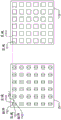
During operation, tuner device 120 receives wireless signal 112 emitted from source 110 to produce wireless output 122. As shown, the tunable device 120 includes a plurality of individually controlled window regions 610 (e.g., window region 610-1, window region 610-2, etc. in each different layer of the tuner device 120) to control the radiation pattern of the wireless output 122 emitted from the tuner device 120.
In one embodiment, the tuner device 120 is configured to include an array of window regions (e.g., tunable radiation apertures such as those in the X-Y plane that are super-surface based, aligned in different layers along the Z-axis).
In this example embodiment, each window region of the tuner device 120 includes 4 super surface layers (such as layers 250-1, 250-2, 250-3, and 250-4) to control the respective outputs. Each layer includes a multi-dimensional array of window regions 610 (e.g., in the X-Y plane) operable to provide control of generation of wireless output 122 (input electromagnetic signal) based on received wireless signals 112 (output electromagnetic signal).
Further, in this example embodiment, first window region 610-1 receives a corresponding first portion of wireless signal 112 emitted from source 110; second window region 610-2 receives a second portion of wireless signal 112 emitted from source 110; and so on.
During operation, the controller 140 generates control settings to control a plurality of individually controlled window regions (i.e., super surface cells) on each layer 250.
In one embodiment, the controller 140 controls or changes the setting of the voltage applied to the window area (i.e., the cells or stacks of the window area) to steer the wireless output 122 to a desired direction. In this case, first window region 610-1 of tuner device 110 controls one or more properties, such as phase and amplitude, of the first portion of received wireless signal 112 to produce a corresponding first portion of wireless output 122 transmitted from first window region 122; second window region 610-1 of tuner device 120 controls the phase and amplitude of a second portion of received wireless signal 112 to produce a corresponding second portion of wireless output 122 transmitted from second window region 610-2; and so on. Each subsequent window region in the corresponding stack contributes to a modification of the received portion of the wireless signal 112 (electromagnetic signal).
As discussed further herein, controlling the phase and amplitude of different window regions (e.g., different super-surface elements) enables control of the wireless output 122 in different directions. In other words, controlling the phase of the various portions of energy output from the respective window regions (each as a controllable RF source) enables the tuner device 120 to direct the wireless output to any suitable angular direction (e.g., up/down and/or left/right with respect to the z-axis). In one embodiment, tuner device 120 supports angular steering of the wireless output in a range between-70 degrees and +70 degrees with respect to the Z-axis, although different embodiments may be configured to support any suitable angular control.
An example of a control window region 610 is further illustrated in fig. 7.
Fig. 7 is an example diagram illustrating details of a front side of a window region according to embodiments herein.
In this example embodiment, window region 610-1 includes a plurality of aligned window regions 750 (such as window region 750-1, window region 750-2, etc.) on respective layers of tuner device 120. Each window area layer (substrate) is made of a low-loss dielectric material on which a metal material 790, such as copper, is deposited to create a conductive path at the periphery of the respective window area layer, as shown. The middle of each window area has no metal layers except for the respective circuit paths, which include components such as varactors and traces 710 that extend to the periphery of the window area. In one embodiment, the periphery of the respective window area layer (strip of metallization layer) is connected to a DC ground. The center of circuit path or trace 710 is driven as a bias by a control voltage provided by controller 140.
Referring to fig. 9, to avoid RF energy from leaking back to the controller 140 from the DC circuit path (such as traces 710 in the window area), embodiments herein include respective RF choke circuits 935 (or alternatively one or more components such as inductors and/or resistors) placed between the vias 910 (coupled to traces 710 on the other side of the window area) and the traces 925 that extend back to the controller 140. Via control signals (applied voltages) generated by controller 140 for traces 925 for corresponding window region 610-1, controller 140 controls the tuning of window region 610-1. That is, the controller 140 generates the control signal 905, which control signal 905 is passed through trace 925, through choke 925 and via 910 to trace 710 coupled to a varactor (or other suitable component) on the opposite side of the window region. In the manner previously discussed, the applied voltage associated with the control signal 905 tunes the window region 610-1 to modify the phase and/or amplitude of the input portion of energy from the wireless signal 112. In a similar manner, controller 140 controls each window region in tuner device 120 by generating a different applied voltage.
Referring again to fig. 7, as further shown, each window region layer 750 (e.g., 750-1, 750-2, 750-3, etc.) includes a respective one or more tuning components, such as varactors 721 and 722. Components 721 and 722 (e.g., diodes 721 and 722) in window region 750-1 are connected in parallel and the controller drives traces 710 with a drive signal. As previously discussed, each of the other window regions 750-2, 750-3, 750-4, etc. are fabricated and patterned in a similar manner as window region 7501.
Thus, during operation, controller 140 generates and applies a corresponding drive signal to traces 710 (part of the circuit path) disposed on the surface (face 770) of a corresponding window region 750-1. Controller 140 drives traces 710 at an appropriate voltage (e.g., a DC voltage or an AC voltage) to control the respective capacitances associated with diode components 721 and 722 and corresponding window regions 750-1, thereby controlling the resonant frequency associated with the respective window regions 750-1. Controller 140 drives each window region of tuner device 120 in a similar manner to control the resonant frequency of the multiple window regions.
In one embodiment, control of the resonant frequency (e.g., via application of a DC voltage) associated with each window region 750 (for a given window region) enables controller 140 to control the respective amplitude and phase associated with the corresponding portion of wireless output 122 that passes through that window region. Thus, each window region (e.g., each super surface cell) is individually controllable. As previously discussed, the stacking of the window regions in the tuner device 120 aligned from layer to layer provides overall control of the electromagnetic energy passing through the window regions. As the electromagnetic signal passes through the window regions in the stack, the respective window regions modify the properties of the passing electromagnetic signal.
Separate control of each different stack of window regions enables beamforming of the original received wireless signal 112.
In other words, controlling the properties of the electromagnetic signal passing through each respective window region (and respective window region layer) enables the controller 140 to control the amplitude and/or phase of different portions of the wireless output 122 to control the amplitude and steer the respective wireless output 122 (electromagnetic signal) to any angular direction relative to the z-axis (e.g., the axis aligned by the window region 750).
Note that tuner device 120 is bi-directional/reciprocal in operation. For example, in the opposite direction, the tuner device 120 may be tuned to receive signals from a desired direction, in which case the stack of window regions modifies the properties of the received portion of electromagnetic energy in the respective window regions. The source 102 (or other suitable resource) may be configured to perform further processing on the received signal (e.g., retrieve any data, apply other processing, etc.).
Fig. 8 is an example diagram illustrating a backside of a window region according to embodiments herein.
As shown, traces 720 disposed on face 660 of layer 250-4 (a layer of window regions) enable controller 140 to pass an appropriate voltage (e.g., a DC control signal) to each respective window region (e.g., window regions 610-1, 610-2, 610-3, etc.) in each respective layer to drive a respective varactor in each window region in a different layer.
The face 660 (the back side of the example layer 250-4) also includes traces 726 to form a DC ground path to the peripheral metallic material of each respective window region associated with the tuner device 110. Each tunable layer of the window region (the window region through which portions of the electromagnetic signal pass) in the tuner device 120 is fabricated and operates in a similar manner.
Fig. 10 is an example diagram illustrating different possible radiation patterns according to embodiments herein.
In this example embodiment, graphs 1011 and 1012 indicate beam steering of tuner device 120 in the E-plane. Fig. 1021 and fig. 1022 indicate beam steering of the tuner apparatus 120 in the H plane. Thus, embodiments herein support two-dimensional beam steering, beamforming, and the like.
As previously discussed, the array of window regions associated with tuner device 120 enables controller 140 to control the amplitude and phase associated with each received portion of wireless signal 112 to steer wireless output 122 to any desired direction.
By way of non-limiting example, example performance associated with one example embodiment of tuner device 120, E-plane, and H-plane is as follows:
e-plane Properties:
gain is 12dBi to 14 dBi;
the average side lobe level is-8 dB;
scanning the coverage range from-40 to 40 degrees;
average back to front ratio (back to front ratio): 13 dB.
H-plane Properties:
gain is 12.5dBi to 14 dBi;
the average side lobe level is-8 dB;
scanning the coverage range from-40 to 40 degrees;
average ratio before and after-15 dB.
Note that these values may vary from embodiment to embodiment.
Fig. 11A is an example side view illustrating a stack including a window region and a corresponding plurality of matching metallization layers (e.g., pads, patches, etc.) according to embodiments herein.
In this example embodiment, the stack 1101 of aligned window regions 750 in the tuner device 120 also includes one or more layers of passive metalized material, such as a layer of material 1150-1 (e.g., pad, patch, etc.), a layer of material 1150-2 (e.g., pad, patch, etc.).
During operation, the tuner device 110 outputs a portion of the energy 112-1 to the aligned window region 750 and the stack 1101 of metallization layers 1150. As previously discussed, controller 140 actively controls window region 750 (window region 750-1, window region 750-2, window region 750-3, etc.).
In this example embodiment, stack 1101 also includes a layer 1150-1 of metallization material and a layer 1150-2 of metallization material. Based on the control of the window area 750 and the presence of the layer of metallization material 1150, the stack 1101 controls properties (such as phase, gain, etc.) of various portions of the input signal 112-1 (electromagnetic energy) to produce the output signal 122-1.
The presence of one or more passive layers 1150 (e.g., pads, patches, etc. of material) reduces the number of active window areas 750 required in the stack to achieve the same or better level of control properties (e.g., phase, amplitude, etc.) of the received portion of input signal 112-1 (which passes through stack 1101 and is output as a corresponding portion of wireless output 122-1). Thus, the presence of the one or more passive layers 1150 reduces the control and manufacturing complexity associated with the tuner apparatus 120.
Note that this example embodiment shows modifications to only a portion of the input signal 112 (such as the portion 112-1 that produces the wireless output 122-1). As previously discussed, tuner device 120 may include any number of stacks that are independently tuned to provide a suitable overall output signal 122.
In one embodiment, the presence of one or more layers of metallization material 1150 (e.g., pads, patches, etc.) reduces the number of tunable layers from four to three at a 24GHz (or other suitable value) frequency as compared to the metallization layer 1150 in previous embodiments that did not operate at a lower frequency.
In addition, the example tuner device 120 including an active layer sandwiched between respective passive metallization regions achieves a full phase change of 2PI (i.e., 360 degree phase coverage). In addition, the optional passive matching layer enhances the overall performance and stability of tuner device 120. With regard to performance, in one non-limiting example embodiment, tuner device 120 described herein enables a beam sweep of-60 degrees to +/-60 degrees. In a manner similar to that previously discussed, the low profile and compactness of tuner device 120 makes it suitable for installation in many different types of applications.
Fig. 11B is an example top view diagram illustrating a window region and a corresponding plurality of matched metallization layers according to embodiments herein.
For purposes of illustration, this non-operational view of the components in stack 1101 shows a top or top view of active areas 750-1, 750-2, etc. and layers of passive operational metallization material such as layer 1150-1 (e.g., pad, patch, etc.), layer 1150-2 (e.g., pad, patch, etc.), etc. Note that the size, thickness, and gauge of material layer 1150 may vary depending on the embodiment and desired signal tuning.
Fig. 12 is an example diagram illustrating an array of stacks of window regions and matching metallization layers according to embodiments herein.
As previously discussed, each stack of components in tuner device 120 (e.g., including one or more window regions 750, one or more layers of metallization material 1150) controls a different portion of the pass-through energy associated with received wireless signal 112.
In this example embodiment, the stack 1101 of tuner devices 120 comprises: i) a first stack 1101 of aligned window regions 750-1, 750-2, and 750-3 operable to receive a first portion of energy from wireless signal 112 emitted from source 110, and ii) a second stack 1102 of aligned window regions 751-1, 751-2, and 751-3 operable to receive a second portion of energy from wireless signal 112 emitted from source 110, iii) a third stack 1103 of aligned window regions operable to receive a third portion of energy from wireless signal 112 emitted from source 110, and so on.
As previously discussed, each aligned window region 750 in the first stack 1101 is tunable to adjust a phase/amplitude associated with the first portion of energy passing through the first stack 1101; each aligned window region 751 in the second stack 1102 is tunable to adjust a phase/amplitude associated with the second portion of energy passing through the first stack 1102; and so on.
As previously discussed, the stack 1101 may be configured to include a first layer 1150-1 of passive metallization material disposed at a first axial end of the first stack 1101; a second layer 1150-2 of passive metallization material of the first stack 1101 is disposed at a second axial end of the first stack 1101 opposite the first axial end of the first stack 1101. As further shown, the stack 1102 may be configured to include a second layer of passive metallization material 1151-1 disposed at a first axial end of the second stack 1102; the second layers 1151-2 of passive metallization material of the second stack 1102 are disposed at a second axial end of the second stack 1102 opposite the first axial end of the second stack 1101, and so on.
Note again that the first passive metalized regions 1150-1, 1151-1, etc. reside on a first substrate (such as layer 250-1 of tuner device 120); window regions 750-1, 751-1, etc. reside on a second substrate (such as layer 250-2 of tuner device 120); window regions 750-2, 751-2, etc. reside on a third substrate (such as layer 250-3 of tuner device 120); window regions 750-3, 751-3, etc. reside on a fourth substrate (such as layer 250-4 of tuner device 120); second passive metallization regions 1150-2, 1151-2, etc. reside on a fifth substrate, such as layer 250-5 of tuner device 120.
As previously discussed, the size of each of the optional one or more passive metallization regions 1150 can also be designed to control the passage of energy.
Fig. 13 is an example block diagram of a computer system to implement any of the operations as previously discussed in accordance with embodiments herein.
Any of the resources discussed herein (e.g., controller 140, etc.) may be configured to include computer processor hardware and/or corresponding executable (software) instructions to perform the various operations discussed herein.
As shown, computer system 1350 of the present example includes an interconnect 1311 that couples a computer-readable storage medium 1313, such as a non-transitory type of medium (which may be any suitable type of hardware storage medium that can store and retrieve digital information) to processor 1313 (computer processor hardware), I/O interface 1314, and communication interface 1317.
I/O interface(s) 1314 support connections to storage 1380 and input resources 1392.
The computer-readable storage medium 1312 may be any hardware storage device, such as memory, optical storage, hard drives, floppy disks, etc. In one embodiment, computer-readable storage medium 1312 stores instructions and/or data.
As shown, computer-readable storage medium 1312 may be encoded with management application 140-1 (e.g., comprising instructions) to perform any of the operations discussed herein.
During operation of one embodiment, processor 1313 accesses computer-readable storage medium 1312 using interconnect 1311 to launch, run, execute, interpret or otherwise execute instructions in management application 140-1 stored on computer-readable storage medium 1312. Execution of the control application 140-1 results in a control process 140-2 to perform any of the operations and/or processes discussed herein.
Those skilled in the art will appreciate that computer system 1350 may include other processes and/or software and hardware components, such as an operating system that controls allocation and use of hardware resources to execute management application 140-1.
According to various embodiments, it is noted that the computer system may reside in any of various types of devices, including but not limited to: mobile computers, wireless communication devices, gateway resources, communication management resources, personal computer systems, wireless devices, wireless access points, base stations, telephony devices, desktop computers, laptop computers, notebook computers, netbook computers, mainframe computer systems, palmtop computers, workstations, network computers, application servers, storage devices, consumer electronics (e.g., cameras, camcorders, set-top boxes, mobile devices, video game machines, handheld video game devices), peripheral devices (e.g., switches, modems, routers, set-top boxes, content management devices, handheld remote control devices), any type of computing or electronic device, and the like. Computer system 850 may reside anywhere or may be included in any suitable resource in any network environment to achieve the functionality as discussed herein.
The functionality supported by the different resources will now be discussed by means of the flow chart in fig. 14. Note that the steps in the flow diagrams below may be performed in any suitable order.
Fig. 14 is a flow diagram 1400 illustrating an example method according to embodiments herein. Note that there is some overlap with respect to the above concepts.
In a process operation 1410, the source 110 receives the input signal 105 from the source 102.
In process operation 1420, source 110 sends out wireless signal 112 to tuner device 120.
In process operation 1430, tuner apparatus 120: i) receives a wireless signal 112 emitted from a source 110, and ii) a controller 140 individually controls a window area of the tuner device 120 to control a radiation pattern of a wireless output emitted from the tuner device.
Fig. 15 is an example top view diagram illustrating a window region and a corresponding plurality of matching metallization layer pads or patches of a layout on a substrate according to embodiments herein.
In the exemplary embodiment, exemplary layer 250-1 (active window region) includes window region 750-1. Region 1532 (the darker shaded region, coupled to the ground reference) represents a metal layer disposed on substrate 250-1. Region 1533 (metal pads driven with a control signal such as a voltage signal) resides in the middle of electromagnetic transmissive window region 750-1. Component 1521 (e.g., a first varactor or other suitable resource) provides coupling from region 1533 to region 1532. Component 1522 (e.g., a second varactor or other suitable resource) also provides coupling from region 1533 to region 1532. Thus, components 1522 and 1523 are connected in parallel to ground. Controller 140 drives region 1533 to a corresponding window region 750-1 with a corresponding voltage signal.
Each window region on layer 250-1 is configured and controlled in a similar manner.
The example layer 1150-1 (passive layer of pads or metal regions) includes a metalized region 1511 (darker region) and an electromagnetically transparent region 1512.
Fig. 16 is an example side view illustrating a stack including a window region and a corresponding plurality of matched metallization pads according to embodiments herein.
In this example embodiment, stack 1601 includes region 1511 (e.g., a metal pad on substrate layer 1150-1), window region 750-1, window region 750-2, window region 750-3, and region 1519 (e.g., a metal pad on substrate layer 1150-2).
As previously discussed, the controller 140 controls the settings of the active layer 750 by applying a respective voltage to each central region (e.g., region 1533, etc.) of the respective window 750.
The stack 1601 receives a portion of the wireless signal 112-1. The combination of the different components in the stack 1601 is operable to modify one or more properties associated with the received wireless signal 112-1 to produce the wireless output 122-1.
Each stack operates to modify the respective received wireless signal to produce a wireless output in a similar manner as described herein.
Fig. 17 is an example diagram illustrating an array of stacks of window regions and matching metallization pad layers according to embodiments herein.
In this example embodiment, source 102 initiates generation of a wireless signal input to tuner device 120 in any suitable manner, such as previously discussed. The tuner device 120 receives a wireless signal 112.
At time frame T1, the controller 140 individually tunes each of the stacks 1601, 1602, 1603, etc. to transmit the wireless output 122-a (e.g., the wireless output 122 and at angle a, including the first data) to the communication device 1651 at time frame T1. At time frame T2, the controller 140 individually tunes each of the stacks 1601, 1602, 1603, etc. to transmit the wireless output 122-B (e.g., at angle B, including the second data) to the communication device 1652 at time frame T2.
Also in this example embodiment, the stack 1601 of the tuner device 120 receives and modifies one or more attributes associated with the wireless signal 112-1 (a portion of the wireless signal 112) according to a respective setting of a corresponding active window region in the stack 1601 driven by the controller 140. The stack 1601 produces a corresponding output signal 122-1 by modification (e.g., phase or other property modification) of the incoming wireless signal 112-1 of the passing wireless (electromagnetic) signal (i.e., the wireless output portion 112-1). Accordingly, the stack 1601 and the corresponding first window region control the phase of the first portion of the received wireless signal 112-1 to produce a corresponding first portion of the wireless output 122-1.
The stack 1602 of the tuner device 120 receives and modifies one or more attributes associated with the received wireless signal 112-2 according to the respective settings of the corresponding active window regions in the stack 1602 driven by the controller 140. The stack 1602 generates the output signal 122-2 (a portion of the wireless output 122) by a modification (e.g., a phase modification) of the input wireless signal 112-2 of the passed wireless signal (a portion of the wireless signal 112-2). Accordingly, the stack 1602 and corresponding second window region control the phase of the second portion of the received wireless signal 112-2 to produce a corresponding second portion of the wireless output 122-2.
The stack 1603 of the tuner device 120 receives and modifies one or more attributes associated with the wireless signal 112-3 according to the respective settings of the corresponding window regions in the stack 1603 driven by the controller 140. The stack 1603 produces the output signal 122-3 by modification (e.g., phase modification) of the input wireless signal 112-3 of the passed wireless signal (a portion of the wireless signal 112-3). Accordingly, the stack 1603 and the corresponding third window area control the phase of the third portion of the received wireless signal 112-3 to produce a corresponding third portion of the wireless output 122-3.
Accordingly, the controller 140 individually tunes each of the plurality of window regions to produce wireless outputs (122-A, 122-B, etc.) from the received wireless signal 112 at different times; the tuned window region modifies different respective portions of the respective wireless signals (112-1, 112-2, 112-3, etc.) passing therethrough.
In summary, at time frame T1, the modification of the input wireless signal 112 via the tuner device 120 and corresponding window region stacking diverts (at angle a relative to the z-axis) the wireless signal 122 (wireless output 122-a and corresponding data payload) to the communication device 1651; at time frame T2, the modification of the input wireless signal 112 via the tuner device 120 diverts (at an angle B relative to the z-axis) the wireless signal (output signal 122-B and corresponding data payload) to the communication device 1652.
Thus, in this example embodiment, controller 140 controls the steering of wireless signals 122-A and 122-B to deliver data/RF power to devices in different spatial locations based on the tuning of the various window regions of tuner device 120 at different times.
Accordingly, embodiments herein include implementing the controller 140 and corresponding variable tuning of the settings of the plurality of separately controlled window regions to variably steer (or beamform) the wireless output 122 (e.g., wireless outputs 122-a, 122-B, etc.) to different desired directions at different times.
Fig. 18 is an example diagram illustrating an array of stacks of window regions and matching metallization pad layers according to embodiments herein.
In the exemplary embodiment, source 102 receives data from a plurality of communication devices 1651 and 1652.
At time frame T11, communication device 1561 communicates wireless signal 122-C (an electromagnetic signal) to tuner device 120 at angle a (relative to the z-axis). At time frame T12, via beam steering or beam forming, the controller 140 individually tunes each of the stacks 1601, 1602, 1603, etc. to receive the wireless signal 122-D (e.g., including fourth data) from the communication device 1652 from angle B (relative to the Z-axis).
Also in this example embodiment, the stack 1601 of the tuner device 120 receives and modifies one or more attributes associated with the received wireless signal 122-C (a portion of the wireless signal 122-1) according to a respective setting of a corresponding window region in the stack 1601 driven by the controller 140. The stack 1601 generates the output signal 112-1 by a modification (e.g., phase modification) of the input wireless signal 122-1. Accordingly, the stack 1601 and the corresponding first window region control the phase of the first portion of the received wireless signal 122-1 to produce a corresponding first portion of the wireless output 112-1.
The stack 1603 of the tuner device 120 receives and modifies one or more attributes associated with the received wireless signal 122-C (a portion of the wireless signal 122-3) according to the respective settings of the corresponding window regions in the stack 1603 driven by the controller 140. The stack 1603 generates the output signal 112-3 by a modification (e.g., phase modification) of the input wireless signal 122-3. Accordingly, the stack 1603 and the corresponding third window area control the phase of the third portion of the received wireless signal 122-3 to produce a corresponding third portion of the wireless output 112-3.
In one embodiment, each of the wireless signals 112-1, 112-2, 112-3, etc. is redirected along or parallel to the z-axis in a direction toward the source 102.
Accordingly, the controller 140 individually tunes each of the plurality of window regions to receive wireless signals (122-C, 122-D, etc.) from the received wireless signal 122 at different times and at different angles; the tuned window region modifies different respective portions of the respective wireless signals (122-1, 122-2, 122-3, etc.) passing therethrough.
Accordingly, controller 140 variably tunes the settings of the plurality of individually controlled window regions to receive wireless signals 122-C and 122-D from different angles at different times.
Fig. 19 is a flow diagram 1900 illustrating an example method according to embodiments herein. Note that there is some overlap with respect to the above concepts.
In a process operation 1910, the system 100 receives an input signal from an input feed component at a source.
In process operation 1920, the source emits a wireless signal based on the received input signal.
In processing operation 1930, the tuner device: i) receive a wireless signal emitted from a source, and ii) individually control window regions of the tuner device to control a radiation pattern of a wireless output emitted from the tuner device.
It is again noted that the techniques discussed herein are well suited for use in applications that support dynamic control of radiation patterns. It should be noted, however, that the embodiments herein are not limited to use in such applications, and that the techniques discussed herein are well suited for other applications as well.
Based on the description set forth herein, numerous specific details have been set forth in order to provide a thorough understanding of the claimed subject matter. However, it will be understood by those skilled in the art that claimed subject matter may be practiced without these specific details. In other instances, methods, devices, systems, etc., that are known to one of ordinary skill have not been described in detail so as not to obscure claimed subject matter. Some portions of the detailed description have been presented in terms of algorithms or symbolic representations of operations on data bits or binary digital signals stored within a computing system memory, such as a computer memory. These algorithmic descriptions or representations are examples of techniques used by those skilled in the data processing arts to convey the substance of their work to others skilled in the art. Generally, the algorithms described herein are considered to be self-consistent sequences of operations or similar processes leading to a desired result. In this context, operations or processing involve physical manipulation of physical quantities. Usually, though not necessarily, these quantities may take the form of electrical or magnetic signals capable of being stored, transferred, combined, compared, and otherwise manipulated. It has proven convenient at times, principally for reasons of common usage, to refer to such signals as bits, data, values, elements, symbols, characters, terms, numbers, numerals or the like. It should be understood, however, that all of these and similar terms are to be associated with the appropriate physical quantities and are merely convenient labels.
While the invention has been particularly shown and described with reference to a preferred embodiment thereof, it will be understood by those skilled in the art that various changes in form and detail may be made therein without departing from the spirit and scope of the invention. Such variations are intended to be covered by the scope of this application. As such, the foregoing description of the embodiments of the application is not intended to be limiting. Rather, any limitations to the invention are presented in the appended claims.
Claims (40)
Applications Claiming Priority (3)
| Application Number | Priority Date | Filing Date | Title |
|---|---|---|---|
| US201862633671P | 2018-02-22 | 2018-02-22 | |
| US62/633,671 | 2018-02-22 | ||
| PCT/US2019/018521 WO2019164813A1 (en) | 2018-02-22 | 2019-02-19 | Antenna hardware and control |
Publications (2)
| Publication Number | Publication Date |
|---|---|
| CN111937232A CN111937232A (en) | 2020-11-13 |
| CN111937232B true CN111937232B (en) | 2021-10-19 |
Family
ID=67688315
Family Applications (1)
| Application Number | Title | Priority Date | Filing Date |
|---|---|---|---|
| CN201980019261.9A Active CN111937232B (en) | 2018-02-22 | 2019-02-19 | Communication device, communication method, and computer-readable storage hardware |
Country Status (5)
| Country | Link |
|---|---|
| US (1) | US11811138B2 (en) |
| EP (1) | EP3756237A4 (en) |
| JP (1) | JP7301058B2 (en) |
| CN (1) | CN111937232B (en) |
| WO (1) | WO2019164813A1 (en) |
Families Citing this family (5)
| Publication number | Priority date | Publication date | Assignee | Title |
|---|---|---|---|---|
| CN110600885B (en) * | 2019-09-04 | 2020-12-29 | 北京理工大学 | A frequency selective surface with absorption-reflection-absorption properties |
| CN116325366B (en) * | 2020-06-11 | 2025-01-10 | 斯凯吉格有限责任公司 | Multi-beam beamforming front-end antenna system for wireless transceiver |
| CN116547868A (en) * | 2020-11-24 | 2023-08-04 | 华为技术有限公司 | Millimeter wave antenna device and module comprising such a device |
| JP7634715B1 (en) * | 2023-06-16 | 2025-02-21 | 京セラ株式会社 | Antenna device and radio wave control board |
| TWI886509B (en) * | 2023-07-12 | 2025-06-11 | 友達光電股份有限公司 | Antenna device and antenna calibration system |
Family Cites Families (38)
| Publication number | Priority date | Publication date | Assignee | Title |
|---|---|---|---|---|
| US5767789A (en) * | 1995-08-31 | 1998-06-16 | International Business Machines Corporation | Communication channels through electrically conducting enclosures via frequency selective windows |
| JP4019639B2 (en) * | 2001-02-07 | 2007-12-12 | 松下電器産業株式会社 | Antenna device |
| US7034636B2 (en) * | 2001-09-20 | 2006-04-25 | Paratek Microwave Incorporated | Tunable filters having variable bandwidth and variable delay |
| US6911957B2 (en) * | 2003-07-16 | 2005-06-28 | Harris Corporation | Dynamically variable frequency selective surface |
| US7190325B2 (en) * | 2004-02-18 | 2007-03-13 | Delphi Technologies, Inc. | Dynamic frequency selective surfaces |
| JP4890473B2 (en) | 2005-01-05 | 2012-03-07 | エイティーシー・テクノロジーズ,リミテッド・ライアビリティ・カンパニー | Adaptive beamforming with multi-user detection and interference reduction in satellite communication systems and methods |
| JP4557169B2 (en) * | 2005-10-03 | 2010-10-06 | 株式会社デンソー | antenna |
| US7671804B2 (en) * | 2006-09-05 | 2010-03-02 | Apple Inc. | Tunable antennas for handheld devices |
| US11063625B2 (en) * | 2008-08-14 | 2021-07-13 | Theodore S. Rappaport | Steerable antenna device |
| US8338991B2 (en) * | 2009-03-20 | 2012-12-25 | Qualcomm Incorporated | Adaptive impedance tuning in wireless power transmission |
| US8374545B2 (en) * | 2009-09-02 | 2013-02-12 | Qualcomm Incorporated | De-tuning in wireless power reception |
| US8811914B2 (en) * | 2009-10-22 | 2014-08-19 | At&T Intellectual Property I, L.P. | Method and apparatus for dynamically processing an electromagnetic beam |
| KR101182400B1 (en) | 2010-12-24 | 2012-09-12 | 전자부품연구원 | Beamforming array antenna control system and method for beamforming |
| US8594584B2 (en) | 2011-05-16 | 2013-11-26 | Blackberry Limited | Method and apparatus for tuning a communication device |
| CA2835432C (en) * | 2011-05-16 | 2016-09-13 | Keith Ronald Manssen | Method and apparatus for tuning a communication device |
| US9041617B2 (en) * | 2011-12-20 | 2015-05-26 | Apple Inc. | Methods and apparatus for controlling tunable antenna systems |
| US9413066B2 (en) | 2012-07-19 | 2016-08-09 | Blackberry Limited | Method and apparatus for beam forming and antenna tuning in a communication device |
| CN102769205A (en) * | 2012-07-24 | 2012-11-07 | 电子科技大学 | A tunable dual-frequency negative refractive index medium based on ferrimagnet and its preparation method |
| CN102790283A (en) * | 2012-07-24 | 2012-11-21 | 电子科技大学 | Adjustable three-frequency negative permeability metamaterial based on ferrimagnetics and manufacturing method thereof |
| US9252492B2 (en) * | 2012-08-29 | 2016-02-02 | Intel Deutschland Gmbh | Antenna tuning via multi-feed transceiver architecture |
| US8908251B2 (en) * | 2013-01-30 | 2014-12-09 | Hrl Laboratories, Llc | Tunable optical metamaterial |
| CN103178351B (en) * | 2013-02-27 | 2016-08-10 | 华中科技大学 | A kind of THz wave Meta Materials manipulator of frequency-adjustable |
| FR3003710B1 (en) * | 2013-03-21 | 2016-07-15 | Tekcem | METHOD AND APPARATUS FOR RADIO RECEPTION USING A PLURALITY OF ANTENNAS AND AMPLIFIER WITH MULTIPLE INPUT ACCESS AND MULTIPLE OUTPUT ACCESS |
| US9434352B2 (en) * | 2013-06-27 | 2016-09-06 | GM Global Technology Operations LLC | Antenna on glass with integral anti-theft feature |
| CN105359338B (en) * | 2013-07-02 | 2018-11-02 | 维斯普瑞公司 | Filtering antenna system, device and method |
| CN103474775B (en) * | 2013-09-06 | 2015-03-11 | 中国科学院光电技术研究所 | Phased array antenna based on dynamic regulation and control artificial electromagnetic structure material |
| FR3021813B1 (en) * | 2014-05-28 | 2017-12-08 | Tekcem | RADIO COMMUNICATION USING A PLURALITY OF SELECTED ANTENNAS |
| US9350835B2 (en) * | 2014-07-23 | 2016-05-24 | Blackberry Limited | Mobile wireless communications device with improved broadband antenna impedance matching |
| KR101694950B1 (en) * | 2015-01-09 | 2017-01-10 | 경희대학교 산학협력단 | Apparatus and method for wireless energy suppliment |
| CN105655721A (en) * | 2015-08-03 | 2016-06-08 | 西安电子科技大学 | Double-waveband composite broadband wave absorbing material based on frequency selective surface |
| US10511092B2 (en) * | 2015-10-27 | 2019-12-17 | Intel Corporation | Orbital angular momentum in millimeter-wave wireless communication |
| EP3247049A1 (en) * | 2016-05-17 | 2017-11-22 | Nxp B.V. | Wireless antenna structure |
| CN205863403U (en) * | 2016-06-15 | 2017-01-04 | 深圳光启高等理工研究院 | Tunable metamaterial structure |
| EP3300172A1 (en) * | 2016-09-22 | 2018-03-28 | British Telecommunications public limited company | Beamsteering using metamaterials |
| CN106876982B (en) * | 2017-02-22 | 2021-08-06 | 西安电子科技大学 | Metasurfaces to improve performance of multi-antenna systems and multi-antenna systems using metasurfaces |
| CN107369918B (en) * | 2017-06-30 | 2020-01-31 | 西安电子科技大学 | Tunable-bandwidth absorber based on graphene and metasurfaces |
| CN107359419A (en) * | 2017-08-22 | 2017-11-17 | 深圳天珑无线科技有限公司 | Antenna system and mobile terminal |
| CN107591626A (en) * | 2017-08-31 | 2018-01-16 | 青岛理工大学 | Beam forming antenna based on PIN diode super surface structure control |
-
2019
- 2019-02-19 EP EP19758159.8A patent/EP3756237A4/en not_active Withdrawn
- 2019-02-19 JP JP2020544247A patent/JP7301058B2/en active Active
- 2019-02-19 US US16/970,777 patent/US11811138B2/en active Active
- 2019-02-19 CN CN201980019261.9A patent/CN111937232B/en active Active
- 2019-02-19 WO PCT/US2019/018521 patent/WO2019164813A1/en not_active Ceased
Also Published As
| Publication number | Publication date |
|---|---|
| WO2019164813A1 (en) | 2019-08-29 |
| JP2021516005A (en) | 2021-06-24 |
| US20210013618A1 (en) | 2021-01-14 |
| JP7301058B2 (en) | 2023-06-30 |
| CN111937232A (en) | 2020-11-13 |
| EP3756237A4 (en) | 2021-11-24 |
| EP3756237A1 (en) | 2020-12-30 |
| US11811138B2 (en) | 2023-11-07 |
Similar Documents
| Publication | Publication Date | Title |
|---|---|---|
| CN111937232B (en) | Communication device, communication method, and computer-readable storage hardware | |
| US20180226727A1 (en) | Module, wireless communication apparatus, and radar apparatus | |
| US9698479B2 (en) | Two-dimensionally electronically-steerable artificial impedance surface antenna | |
| US10468777B2 (en) | Luneburg lens antenna device | |
| EP2201646B1 (en) | Dual polarized low profile antenna | |
| WO2021236921A1 (en) | Dual-band cross-polarized 5g mm-wave phased array antenna | |
| Gu et al. | 3-D coverage beam-scanning antenna using feed array and active frequency-selective surface | |
| US11050160B2 (en) | Planar-shaped antenna devices, antenna arrays, and fabrication | |
| CN210272694U (en) | Substrate integrated waveguide slot scanning antenna | |
| JP2016036129A (en) | Surface wave waveguides with conductive sidewalls and applications in antennas. | |
| US10886604B2 (en) | Interleaved array of antennas operable at multiple frequencies | |
| CN112234341B (en) | Antenna assembly and electronic equipment | |
| CN113013606B (en) | Adjustable array antenna based on substrate integrated waveguide and terminal | |
| CN111052507B (en) | Antenna and wireless device | |
| CN113097736A (en) | Novel frequency and wave beam reconfigurable antenna | |
| CN110212299B (en) | Array antenna module with adjustable element factors | |
| US20210384632A1 (en) | Antenna and antenna module | |
| JPS58141006A (en) | Diversity antenna for circular polarized wave | |
| JP6978186B2 (en) | Two-dimensional, electronically steerable artificial impedance surface antenna | |
| US11482794B1 (en) | Slot-fed unit cell and current sheet array | |
| US20250038400A1 (en) | Beam-steering antenna systems | |
| Neebha et al. | Analysis of multilayered antennas with slotted ground for bandwidth enhancement | |
| Liang et al. | Wideband dual‐polarized wide solid angle scanning cylindrically conformal millimeter‐wave phased array | |
| CN120051896A (en) | Antenna and communication method |
Legal Events
| Date | Code | Title | Description |
|---|---|---|---|
| PB01 | Publication | ||
| PB01 | Publication | ||
| SE01 | Entry into force of request for substantive examination | ||
| SE01 | Entry into force of request for substantive examination | ||
| GR01 | Patent grant | ||
| GR01 | Patent grant |