CN111934630A - Envelope tracking power modulator and related methods and systems - Google Patents
Envelope tracking power modulator and related methods and systems Download PDFInfo
- Publication number
- CN111934630A CN111934630A CN202010331948.0A CN202010331948A CN111934630A CN 111934630 A CN111934630 A CN 111934630A CN 202010331948 A CN202010331948 A CN 202010331948A CN 111934630 A CN111934630 A CN 111934630A
- Authority
- CN
- China
- Prior art keywords
- zero
- circuit
- peak
- envelope tracking
- frequency
- Prior art date
- Legal status (The legal status is an assumption and is not a legal conclusion. Google has not performed a legal analysis and makes no representation as to the accuracy of the status listed.)
- Granted
Links
Images


Classifications
-
- H—ELECTRICITY
- H03—ELECTRONIC CIRCUITRY
- H03F—AMPLIFIERS
- H03F1/00—Details of amplifiers with only discharge tubes, only semiconductor devices or only unspecified devices as amplifying elements
- H03F1/02—Modifications of amplifiers to raise the efficiency, e.g. gliding Class A stages, use of an auxiliary oscillation
- H03F1/0205—Modifications of amplifiers to raise the efficiency, e.g. gliding Class A stages, use of an auxiliary oscillation in transistor amplifiers
- H03F1/0211—Modifications of amplifiers to raise the efficiency, e.g. gliding Class A stages, use of an auxiliary oscillation in transistor amplifiers with control of the supply voltage or current
- H03F1/0216—Continuous control
- H03F1/0233—Continuous control by using a signal derived from the output signal, e.g. bootstrapping the voltage supply
-
- H—ELECTRICITY
- H03—ELECTRONIC CIRCUITRY
- H03F—AMPLIFIERS
- H03F1/00—Details of amplifiers with only discharge tubes, only semiconductor devices or only unspecified devices as amplifying elements
- H03F1/02—Modifications of amplifiers to raise the efficiency, e.g. gliding Class A stages, use of an auxiliary oscillation
- H03F1/0205—Modifications of amplifiers to raise the efficiency, e.g. gliding Class A stages, use of an auxiliary oscillation in transistor amplifiers
- H03F1/0211—Modifications of amplifiers to raise the efficiency, e.g. gliding Class A stages, use of an auxiliary oscillation in transistor amplifiers with control of the supply voltage or current
- H03F1/0216—Continuous control
- H03F1/0222—Continuous control by using a signal derived from the input signal
-
- H—ELECTRICITY
- H03—ELECTRONIC CIRCUITRY
- H03F—AMPLIFIERS
- H03F1/00—Details of amplifiers with only discharge tubes, only semiconductor devices or only unspecified devices as amplifying elements
- H03F1/42—Modifications of amplifiers to extend the bandwidth
-
- H—ELECTRICITY
- H03—ELECTRONIC CIRCUITRY
- H03F—AMPLIFIERS
- H03F1/00—Details of amplifiers with only discharge tubes, only semiconductor devices or only unspecified devices as amplifying elements
- H03F1/02—Modifications of amplifiers to raise the efficiency, e.g. gliding Class A stages, use of an auxiliary oscillation
-
- H—ELECTRICITY
- H03—ELECTRONIC CIRCUITRY
- H03F—AMPLIFIERS
- H03F1/00—Details of amplifiers with only discharge tubes, only semiconductor devices or only unspecified devices as amplifying elements
- H03F1/32—Modifications of amplifiers to reduce non-linear distortion
- H03F1/3241—Modifications of amplifiers to reduce non-linear distortion using predistortion circuits
-
- H—ELECTRICITY
- H03—ELECTRONIC CIRCUITRY
- H03F—AMPLIFIERS
- H03F3/00—Amplifiers with only discharge tubes or only semiconductor devices as amplifying elements
- H03F3/189—High-frequency amplifiers, e.g. radio frequency amplifiers
- H03F3/19—High-frequency amplifiers, e.g. radio frequency amplifiers with semiconductor devices only
- H03F3/193—High-frequency amplifiers, e.g. radio frequency amplifiers with semiconductor devices only with field-effect devices
-
- H—ELECTRICITY
- H03—ELECTRONIC CIRCUITRY
- H03F—AMPLIFIERS
- H03F3/00—Amplifiers with only discharge tubes or only semiconductor devices as amplifying elements
- H03F3/20—Power amplifiers, e.g. Class B amplifiers, Class C amplifiers
- H03F3/21—Power amplifiers, e.g. Class B amplifiers, Class C amplifiers with semiconductor devices only
- H03F3/211—Power amplifiers, e.g. Class B amplifiers, Class C amplifiers with semiconductor devices only using a combination of several amplifiers
-
- H—ELECTRICITY
- H03—ELECTRONIC CIRCUITRY
- H03F—AMPLIFIERS
- H03F3/00—Amplifiers with only discharge tubes or only semiconductor devices as amplifying elements
- H03F3/20—Power amplifiers, e.g. Class B amplifiers, Class C amplifiers
- H03F3/24—Power amplifiers, e.g. Class B amplifiers, Class C amplifiers of transmitter output stages
- H03F3/245—Power amplifiers, e.g. Class B amplifiers, Class C amplifiers of transmitter output stages with semiconductor devices only
-
- H—ELECTRICITY
- H03—ELECTRONIC CIRCUITRY
- H03F—AMPLIFIERS
- H03F3/00—Amplifiers with only discharge tubes or only semiconductor devices as amplifying elements
- H03F3/45—Differential amplifiers
- H03F3/45071—Differential amplifiers with semiconductor devices only
- H03F3/45076—Differential amplifiers with semiconductor devices only characterised by the way of implementation of the active amplifying circuit in the differential amplifier
- H03F3/45179—Differential amplifiers with semiconductor devices only characterised by the way of implementation of the active amplifying circuit in the differential amplifier using MOSFET transistors as the active amplifying circuit
- H03F3/45183—Long tailed pairs
-
- H—ELECTRICITY
- H03—ELECTRONIC CIRCUITRY
- H03G—CONTROL OF AMPLIFICATION
- H03G5/00—Tone control or bandwidth control in amplifiers
- H03G5/16—Automatic control
- H03G5/24—Automatic control in frequency-selective amplifiers
- H03G5/28—Automatic control in frequency-selective amplifiers having semiconductor devices
-
- H—ELECTRICITY
- H03—ELECTRONIC CIRCUITRY
- H03F—AMPLIFIERS
- H03F2200/00—Indexing scheme relating to amplifiers
- H03F2200/102—A non-specified detector of a signal envelope being used in an amplifying circuit
-
- H—ELECTRICITY
- H03—ELECTRONIC CIRCUITRY
- H03F—AMPLIFIERS
- H03F2200/00—Indexing scheme relating to amplifiers
- H03F2200/451—Indexing scheme relating to amplifiers the amplifier being a radio frequency amplifier
-
- H—ELECTRICITY
- H03—ELECTRONIC CIRCUITRY
- H03F—AMPLIFIERS
- H03F2203/00—Indexing scheme relating to amplifiers with only discharge tubes or only semiconductor devices as amplifying elements covered by H03F3/00
- H03F2203/45—Indexing scheme relating to differential amplifiers
- H03F2203/45372—Indexing scheme relating to differential amplifiers the AAC comprising one or more potentiometers
-
- H—ELECTRICITY
- H03—ELECTRONIC CIRCUITRY
- H03F—AMPLIFIERS
- H03F2203/00—Indexing scheme relating to amplifiers with only discharge tubes or only semiconductor devices as amplifying elements covered by H03F3/00
- H03F2203/45—Indexing scheme relating to differential amplifiers
- H03F2203/45376—Indexing scheme relating to differential amplifiers the AAC comprising one or more discrete resistors as shunts between collectors or drains
-
- H—ELECTRICITY
- H03—ELECTRONIC CIRCUITRY
- H03G—CONTROL OF AMPLIFICATION
- H03G2201/00—Indexing scheme relating to subclass H03G
- H03G2201/10—Gain control characterised by the type of controlled element
- H03G2201/103—Gain control characterised by the type of controlled element being an amplifying element
-
- H—ELECTRICITY
- H03—ELECTRONIC CIRCUITRY
- H03G—CONTROL OF AMPLIFICATION
- H03G2201/00—Indexing scheme relating to subclass H03G
- H03G2201/30—Gain control characterized by the type of controlled signal
- H03G2201/307—Gain control characterized by the type of controlled signal being radio frequency signal
-
- H—ELECTRICITY
- H03—ELECTRONIC CIRCUITRY
- H03G—CONTROL OF AMPLIFICATION
- H03G3/00—Gain control in amplifiers or frequency changers
- H03G3/20—Automatic control
- H03G3/30—Automatic control in amplifiers having semiconductor devices
- H03G3/3036—Automatic control in amplifiers having semiconductor devices in high-frequency amplifiers or in frequency-changers
- H03G3/3042—Automatic control in amplifiers having semiconductor devices in high-frequency amplifiers or in frequency-changers in modulators, frequency-changers, transmitters or power amplifiers
-
- H—ELECTRICITY
- H04—ELECTRIC COMMUNICATION TECHNIQUE
- H04B—TRANSMISSION
- H04B1/00—Details of transmission systems, not covered by a single one of groups H04B3/00 - H04B13/00; Details of transmission systems not characterised by the medium used for transmission
- H04B1/38—Transceivers, i.e. devices in which transmitter and receiver form a structural unit and in which at least one part is used for functions of transmitting and receiving
- H04B1/40—Circuits
Landscapes
- Engineering & Computer Science (AREA)
- Power Engineering (AREA)
- Computer Networks & Wireless Communication (AREA)
- Signal Processing (AREA)
- Physics & Mathematics (AREA)
- Nonlinear Science (AREA)
- Amplifiers (AREA)
- Transmitters (AREA)
Abstract
本发明提供了一种包络跟踪电源调制器,其包括放大器电路和零峰值电路。放大器电路接收包络输入,根据该包络输入产生已调制的电源电压,并将该已调制的电源电压提供给功率放大器。零峰值电路耦接于放大器电路,并且给放大器电路应用零峰值,其中,零峰值在频率处插入零点。相应地,本发明还提供了一种无线通信系统及包络跟踪校准方法,通过零峰值电路在频率处插入零点能够增大包络跟踪的带宽且无需额外的静态电流消耗。
The present invention provides an envelope tracking power modulator, which includes an amplifier circuit and a zero peak circuit. The amplifier circuit receives an envelope input, generates a modulated power supply voltage according to the envelope input, and provides the modulated power supply voltage to a power amplifier. The zero peak circuit is coupled to the amplifier circuit and applies a zero peak value to the amplifier circuit, wherein the zero peak value inserts a zero point at a frequency. Accordingly, the present invention also provides a wireless communication system and an envelope tracking calibration method, wherein the zero peak circuit inserts a zero point at a frequency to increase the bandwidth of envelope tracking without requiring additional static current consumption.
Description
技术领域technical field
本发明涉及包络跟踪,以及更具体地,涉及具有零峰值(with zero peaking)的包络跟踪电源调制器以及相关的包络跟踪校准方法和系统。The present invention relates to envelope tracking, and more particularly, to envelope tracking power supply modulators with zero peaking and related envelope tracking calibration methods and systems.
背景技术Background technique
功率放大器(power amplifier,PA)用于放大射频(radio-frequency,RF)信号,以进行无线电传输。功率放大器(PA)在用于驱动发射器的一个或多个天线的无线通信装置中很常见。功率放大器(PA)的功耗(power consumption)对电池供电的无线通信装置来说至关重要。传统上,功率放大器(PA)被固定的电源电压偏置。当输入到功率放大器(PA)的RF输入信号处于最大电平(level)时,通常会出现峰值(Peak)RF输出功率情况。然而,当功率放大器从该峰值RF输出功率情况退出时,多余的输入功率必须由功率放大器(PA)消散掉,因为这些多余的输入功率没有被转换成有用的射频RF输出功率。也就是说,传统的固定PA电源电压会导致大量的功率损耗(如热量)。包络跟踪是一项要求利用RF输入信号的包络对功率放大器(PA)的供电电压进行动态调制的技术。这将使得功率放大器(PA)总是保持为接近峰值电平操作,并大大提高了功率放大器(PA)的效率。即,包络跟踪技术调制PA电源电压来跟踪RF输入信号的包络,以减少作为热量散发的功率。A power amplifier (PA) is used to amplify a radio-frequency (RF) signal for radio transmission. Power amplifiers (PAs) are common in wireless communication devices used to drive one or more antennas of a transmitter. The power consumption of a power amplifier (PA) is critical for battery powered wireless communication devices. Traditionally, power amplifiers (PAs) are biased by a fixed supply voltage. Peak RF output power conditions typically occur when the RF input signal to the power amplifier (PA) is at its maximum level. However, when the power amplifier is withdrawn from this peak RF output power condition, the excess input power must be dissipated by the power amplifier (PA) because this excess input power is not converted into useful radio frequency RF output power. That said, traditional fixed PA supply voltages result in significant power losses (such as heat). Envelope tracking is a technique that requires dynamic modulation of the power amplifier (PA) supply voltage using the envelope of the RF input signal. This will keep the power amplifier (PA) always operating close to the peak level and greatly improve the efficiency of the power amplifier (PA). That is, envelope tracking techniques modulate the PA supply voltage to track the envelope of the RF input signal to reduce the power dissipated as heat.
在无线通信中,带宽是调制载波信号所占据的频率范围。随着无线通信技术的进步,一个调制载波信号使用越来越宽的带宽。因此,包络跟踪电源调制器(其用于向PA提供已调制的电源电压)需要宽带宽(wide bandwidth)线性放大器。通常,线性放大器的跨导(偏置电流)被增加,以增强带宽和线性度。由于线性放大器需要大的偏置电流才能将主极点(dominant pole)推至更高的频率,因此,传统的宽带宽包络跟踪设计会耗费大量功率。此外,考虑到使用成熟工艺(例如18nm工艺)制造包络跟踪电源调制器的情况,对于宽带宽包络跟踪,线性放大器的静态电流(quiescent current)急剧增加。In wireless communications, bandwidth is the frequency range occupied by the modulated carrier signal. As wireless communication technology advances, a modulated carrier signal uses wider and wider bandwidths. Therefore, the envelope tracking supply modulator, which is used to provide the modulated supply voltage to the PA, requires a wide bandwidth linear amplifier. Typically, the transconductance (bias current) of a linear amplifier is increased to enhance bandwidth and linearity. Traditional wide bandwidth envelope tracking designs consume a lot of power because linear amplifiers require large bias currents to push the dominant pole to higher frequencies. Furthermore, considering the case of using a mature process (eg, 18nm process) to fabricate envelope tracking power supply modulators, the quiescent current of the linear amplifier increases dramatically for wide bandwidth envelope tracking.
因此,需要一种能够实现宽带宽包络跟踪而又不会增加静态电流消耗的创新设计。Therefore, there is a need for an innovative design that enables wide bandwidth envelope tracking without increasing quiescent current consumption.
发明内容SUMMARY OF THE INVENTION
有鉴于此,本发明的目的之一在于提供一种具有零峰值的包络跟踪电源调制器及相关的无线通信系统及包络跟踪校准方法,其可以增大包络跟踪的带宽且无需额外的静态电流消耗。In view of this, one of the objectives of the present invention is to provide an envelope tracking power modulator with zero peak value, a related wireless communication system, and an envelope tracking calibration method, which can increase the bandwidth of envelope tracking and do not require additional quiescent current consumption.
第一方面,本发明提供了一种包络跟踪电源调制器,包括放大器电路和零峰值电路。放大器电路被布置为接收包络输入、根据该包络输入产生已调制的电源电压,并将该已调制的电源电压提供给功率放大器。零峰值电路耦接于该放大器电路,并用于给该放大器电路应用零峰值,其中,该零峰值在频率处插入零点。In a first aspect, the present invention provides an envelope tracking power supply modulator, including an amplifier circuit and a zero-peak circuit. The amplifier circuit is arranged to receive an envelope input, generate a modulated supply voltage from the envelope input, and provide the modulated supply voltage to the power amplifier. A zero-peak circuit is coupled to the amplifier circuit and is used to apply a zero-peak value to the amplifier circuit, wherein the zero-peak value inserts a zero at the frequency.
在一些实施例中,由该零峰值插入的该零点的频率等于主极点频率。In some embodiments, the frequency of the zero interpolated by the zero peak is equal to the dominant pole frequency.
在一些实施例中,该零峰值电路是可调整的,以及,该零峰值电路可以包括频率调整电路,其用于调整由该零峰值插入的该零点的频率。例如,可以预先设定对应于多个频率(如多个极点对应的频率,但并不限于此,例如,位于主极点频率附近的多个频率)的多个零峰值设置,并在该多个零峰值设置中的每个设置下通过测量ACLR来从该多个零峰值设置中选择最佳的目标零峰值设置(如选取最小的ACLR所对应的零峰值设置)。In some embodiments, the zero-peak circuit is adjustable, and the zero-peak circuit may include a frequency adjustment circuit for adjusting the frequency of the zero inserted by the zero-peak. For example, a plurality of zero-peak settings corresponding to a plurality of frequencies (such as frequencies corresponding to a plurality of poles, but not limited thereto, for example, a plurality of frequencies located near the main pole frequency) may be preset, and Under each of the zero-peak settings, an optimal target zero-peak setting is selected from the multiple zero-peak settings by measuring the ACLR (for example, the zero-peak setting corresponding to the smallest ACLR is selected).
在一些实施例中,该零峰值电路是可调整的,以及,该零峰值电路包括增益调整电路,其用于调整由该零峰值插入的该零点所引入的增益。例如,针对相同的零点频率存在对应于多个增益的多个零峰值设置,并在该多个零峰值设置中的每个设置下通过测量ACLR来从该多个零峰值设置中选择最佳的目标零峰值设置(如选取最小的ACLR所对应的零峰值设置)。In some embodiments, the zero-peak circuit is adjustable, and the zero-peak circuit includes a gain adjustment circuit for adjusting the gain introduced by the zero inserted by the zero-peak. For example, there are multiple zero-peak settings corresponding to multiple gains for the same zero-point frequency, and the best one is selected from the multiple zero-peak settings by measuring ACLR at each of the multiple zero-peak settings Target zero-peak setting (such as selecting the zero-peak setting corresponding to the smallest ACLR).
第二方面,本发明还提供了一种无线通信系统,包括:发送(TX)电路,用于接收TX基带信号,根据该TX基带信号产生射频(RF)信号,并经由功率放大器PA输出该RF信号;包络跟踪电路,用于从该TX基带信号获得包络输入,并根据该包络输入产生已调制的电源电压,其中,该包络跟踪电路包络跟踪电源调制器,以及,该包络跟踪电源调制器包括放大器电路和可调零峰值电路;该放大器电路用于接收该包络输入,根据该包络输入产生该已调制的电源电压,并将该已调制的电源电压提供给该PA;该可调零峰值电路耦接于该放大器电路并用于给该放大器电路应用零峰值,其中,该零峰值在频率处插入零点;接收(RX)电路,用于接收该PA的输出,并从该PA的输出获得RX基带信号;以及,包络跟踪校准电路,用于通过分析该RX基带信号来校准该可调零峰值电路。In a second aspect, the present invention also provides a wireless communication system, comprising: a transmitting (TX) circuit for receiving a TX baseband signal, generating a radio frequency (RF) signal according to the TX baseband signal, and outputting the RF signal via a power amplifier PA a signal; an envelope tracking circuit for obtaining an envelope input from the TX baseband signal and generating a modulated supply voltage from the envelope input, wherein the envelope tracking circuit envelope tracks the supply modulator, and the envelope The network tracking power supply modulator includes an amplifier circuit and an adjustable zero-peak value circuit; the amplifier circuit is used to receive the envelope input, generate the modulated power supply voltage according to the envelope input, and provide the modulated power supply voltage to the PA; the adjustable zero-peak circuit is coupled to the amplifier circuit and used to apply a zero-peak value to the amplifier circuit, wherein the zero-peak value inserts a zero at the frequency; a receive (RX) circuit is used to receive the output of the PA, and An RX baseband signal is obtained from the output of the PA; and an envelope tracking calibration circuit for calibrating the adjustable zero-peak circuit by analyzing the RX baseband signal.
在一些实施例中,该可调零峰值电路包括:频率调整电路,用于调整由该零峰值插入的该零点的频率,其中,该频率调整电路在该包络跟踪校准电路的控制下操作。例如,从对应于多个频率的多个零峰值设置中选择最佳的目标零峰值设置。In some embodiments, the adjustable zero peak circuit includes a frequency adjustment circuit for adjusting the frequency of the zero inserted by the zero peak, wherein the frequency adjustment circuit operates under the control of the envelope tracking calibration circuit. For example, the optimal target zero-peak setting is selected from among multiple zero-peak settings corresponding to multiple frequencies.
在一些实施例中,该可调零峰值电路包括:增益调整电路,用于调整由该零峰值插入的该零点所引入的增益,其中,该增益调整电路在该包络跟踪校准电路的控制下操作。例如,从针对相同频率对应于多个增益的多个零峰值设置中选择最佳的目标零峰值设置。In some embodiments, the adjustable zero-peak circuit includes a gain adjustment circuit for adjusting the gain introduced by the zero inserted by the zero-peak, wherein the gain adjustment circuit is under the control of the envelope tracking calibration circuit operate. For example, the optimal target zero-peak setting is selected from among multiple zero-peak settings corresponding to multiple gains for the same frequency.
在一些实施例中,该包络跟踪校准电路用于根据该RX基带信号计算相邻通道泄漏比(ACLR),并根据该ACLR自适应地校准该可调零峰值电路。In some embodiments, the envelope tracking calibration circuit is used to calculate the adjacent channel leakage ratio (ACLR) from the RX baseband signal, and to adaptively calibrate the adjustable zero peak circuit according to the ACLR.
在一些实施例中,该可调零峰值电路被布置为支持多个预定的零峰值设置,且该包络跟踪校准电路参考该ACLR来选择该多个预定的零峰值设置中的一者作为该可调零峰值电路的目标零峰值设置。In some embodiments, the adjustable zero-peak circuit is arranged to support a plurality of predetermined zero-peak settings, and the envelope tracking calibration circuit refers to the ACLR to select one of the plurality of predetermined zero-peak settings as the The target zero-peak setting for the adjustable zero-peak circuit.
第三方面,本发明提供了一种包络跟踪校准方法,包括:对发射(TX)基带信号进行接收,根据该TX基带信号产生射频(RF)信号,并经由功率放大器PA输出该RF信号;从该TX基带信号获得包络输入;放大器电路根据该包络输入产生已调制的电源电压;提供该已调制的电源电压给该PA;给该放大器电路应用零峰值,其中,该零峰值在频率处插入零点;接收该PA的输出,并从该PA的输出获得接收RX基带信号;以及,通过分析该RX基带信号来校准该零峰值。In a third aspect, the present invention provides an envelope tracking calibration method, comprising: receiving a transmit (TX) baseband signal, generating a radio frequency (RF) signal according to the TX baseband signal, and outputting the RF signal via a power amplifier PA; An envelope input is obtained from the TX baseband signal; an amplifier circuit generates a modulated supply voltage from the envelope input; the modulated supply voltage is provided to the PA; a zero peak is applied to the amplifier circuit, wherein the zero peak is at frequency inserting a zero at the PA; receiving the output of the PA and obtaining a received RX baseband signal from the output of the PA; and calibrating the zero peak by analyzing the RX baseband signal.
在一些实施例中,校准该零峰值包括:调整由该零峰值插入的该零点的频率。In some embodiments, calibrating the zero peak includes adjusting the frequency of the zero interpolated by the zero peak.
在一些实施例中,校准该零峰值包括:调整由该零峰值插入的该零点所引入的增益。In some embodiments, calibrating the zero peak includes adjusting the gain introduced by the zero inserted by the zero peak.
在一些实施例中,通过分析该RX基带信号来校准该零峰值包括:根据该RX基带信号计算相邻通道泄漏比ACLR;以及,根据该ACLR自适应地校准该零峰值。In some embodiments, calibrating the zero peak by analyzing the RX baseband signal includes: calculating an adjacent channel leakage ratio ACLR based on the RX baseband signal; and adaptively calibrating the zero peak based on the ACLR.
在一些实施例中,根据该ACLR自适应地校准该零峰值包括:根据该ACLR选择多个预定的零峰值设置中的一者作为该零峰值的目标零峰值设置。In some embodiments, adaptively calibrating the zero peak based on the ACLR includes selecting one of a plurality of predetermined zero peak settings as the target zero peak setting for the zero peak based on the ACLR.
本领域技术人员在阅读附图所示优选实施例的下述详细描述之后,可以毫无疑义地理解本发明的这些目的及其它目的。详细的描述将参考附图在下面的实施例中给出。These and other objects of the present invention will no doubt be understood by those skilled in the art after reading the following detailed description of the preferred embodiments illustrated in the accompanying drawings. A detailed description will be given in the following embodiments with reference to the accompanying drawings.
附图说明Description of drawings
通过阅读后续的详细描述以及参考附图所给的示例,可以更全面地理解本发明。A more complete understanding of the present invention may be obtained by reading the following detailed description and the examples given with reference to the accompanying drawings.
图1是根据本发明实施例示出的包络跟踪电源调制器的方框示意图。FIG. 1 is a schematic block diagram of an envelope tracking power supply modulator according to an embodiment of the present invention.
图2是根据本发明实施例示出的具有零峰值的包络跟踪电源调制器的一部分的电路示意图。2 is a schematic circuit diagram of a portion of an envelope tracking power supply modulator with zero peak value according to an embodiment of the present invention.
图3是根据本发明实施例示出的无线通信系统的方框示意图。FIG. 3 is a schematic block diagram of a wireless communication system according to an embodiment of the present invention.
图4是根据本发明实施例示出的在不同的零峰值设置下的包络跟踪电源调制器的频率响应的示意图。FIG. 4 is a schematic diagram illustrating the frequency response of an envelope tracking power supply modulator under different zero-peak settings according to an embodiment of the present invention.
在下面的详细描述中,为了说明的目的,阐述了许多具体细节,以便本领域技术人员能够更透彻地理解本发明实施例。然而,显而易见的是,可以在没有这些具体细节的情况下实施一个或多个实施例,不同的实施例可根据需求相结合,而并不应当仅限于附图所列举的实施例。In the following detailed description, for the purposes of explanation, numerous specific details are set forth so that those skilled in the art can more thoroughly understand the embodiments of the present invention. It will be apparent, however, that one or more embodiments may be practiced without these specific details, that different embodiments may be combined as desired, and should not be limited to those illustrated in the accompanying drawings.
具体实施方式Detailed ways
以下描述为本发明实施的较佳实施例,其仅用来例举阐释本发明的技术特征,而并非用来限制本发明的范畴。在通篇说明书及权利要求书当中使用了某些词汇来指称特定的元件,所属领域技术人员应当理解,制造商可能会使用不同的名称来称呼同样的元件。因此,本说明书及权利要求书并不以名称的差异作为区别元件的方式,而是以元件在功能上的差异作为区别的基准。本发明中使用的术语“元件”、“系统”和“装置”可以是与计算机相关的实体,其中,该计算机可以是硬件、软件、或硬件和软件的结合。在以下描述和权利要求书当中所提及的术语“包含”和“包括”为开放式用语,故应解释成“包含,但不限定于…”的意思。此外,术语“耦接”意指间接或直接的电气连接。因此,若文中描述一个装置耦接于另一装置,则代表该装置可直接电气连接于该另一装置,或者透过其它装置或连接手段间接地电气连接至该另一装置。The following description is a preferred embodiment of the present invention, which is only used to illustrate the technical characteristics of the present invention, but not to limit the scope of the present invention. Certain terms are used throughout the specification and claims to refer to particular elements, it being understood by those skilled in the art that manufacturers may refer to the same elements by different names. Therefore, the present specification and claims do not take the difference in name as a way to distinguish elements, but take the difference in function of the elements as a basis for distinction. The terms "element," "system," and "apparatus" as used in the present invention can be a computer-related entity, wherein the computer can be hardware, software, or a combination of hardware and software. The terms "comprising" and "including" mentioned in the following description and claims are open-ended terms and should be interpreted as meaning "including, but not limited to...". Furthermore, the term "coupled" means an indirect or direct electrical connection. Therefore, if a device is described as being coupled to another device, it means that the device can be electrically connected to the other device directly, or indirectly electrically connected to the other device through other devices or connecting means.
其中,除非另有指示,各附图的不同附图中对应的数字和符号通常涉及相应的部分。所绘制的附图清楚地说明了实施例的相关部分且并不一定是按比例绘制。Corresponding numerals and symbols in the different figures of the drawings generally refer to corresponding parts unless otherwise indicated. The drawings are drawn to clearly illustrate relevant parts of the embodiments and are not necessarily drawn to scale.
文中所用术语“基本”或“大致”是指在可接受的范围内,本领域技术人员能够解决所要解决的技术问题,基本达到所要达到的技术效果。举例而言,“大致等于”是指在不影响结果正确性时,技术人员能够接受的与“完全等于”有一定误差的方式。The term "substantially" or "substantially" used herein means that within an acceptable range, those skilled in the art can solve the technical problem to be solved and basically achieve the technical effect to be achieved. For example, "approximately equal to" refers to a manner acceptable to a skilled person with a certain error from "exactly equal to" without affecting the correctness of the result.
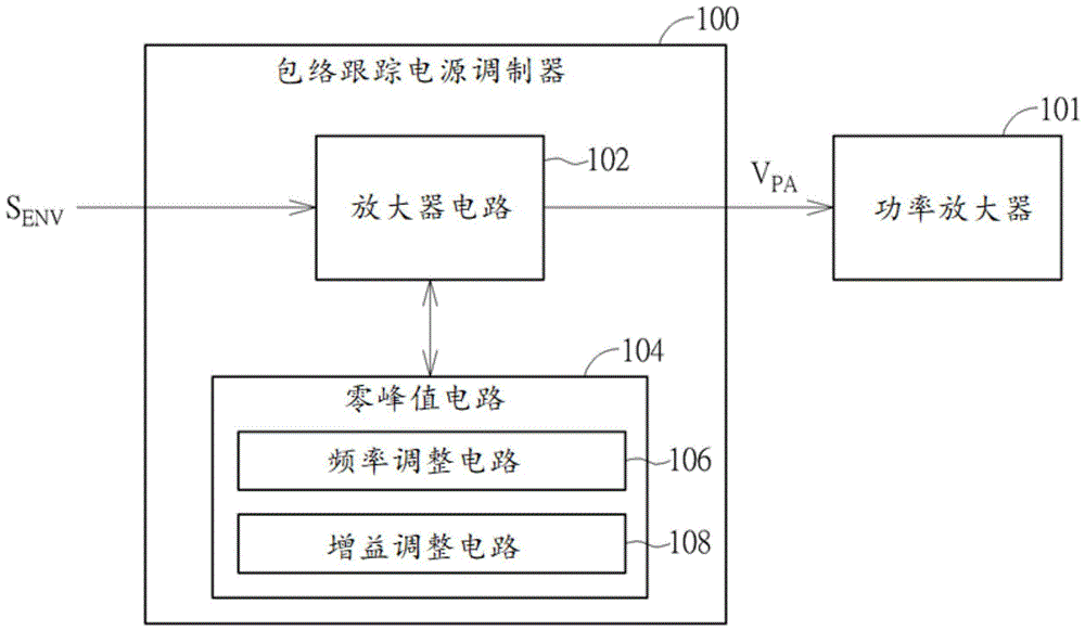
图1是根据本发明实施例示出的包络跟踪电源调制器(envelope trackingsupply modulator,ETSM)的方框示意图。包络跟踪电源调制器100包括放大器电路(amplifier circuit)102和零峰值电路(zero peaking circuit)104。放大器电路102用于接收包络输入SENV,根据包络输入SENV产生已调制的电源电压(modulated supply voltage)VPA,并将已调制的电源电压VPA提供至功率放大器(PA)101。零峰值电路104耦接于放大器电路102,并被设置为给放大器电路102施加/应用(apply)零峰值(zero peaking),其中,所述零峰值在选定频率(selected frequency)处插入附加的零点(zero),从而将主极点(dominant pole)推(push)至更高的频率或者使得主极点频率变得更高。例如,没有(without)零峰值的放大器电路102具有原始的主极点频率(original dominant polefrequency)。利用/具有(with)零峰值的放大器电路102具有零峰值频率(该零峰值频率位于该原始的主极点频率处或在其附近,即零峰值频率大致等于主极点频率),以补偿在该原始的主极点频率处的放大器增益损耗。也就是说,在本发明实施例中,上述选定频率等于或大致等于放大器电路102/包络跟踪电源调制器100的主极点频率。以此方式,可以增大包络跟踪的带宽且无需额外的静态电流消耗。例如,3dB频率可以高于100MHz。可以理解地,假定在不具有零峰值电路104的情况下,包络跟踪电源调制器100的传递函数为H(s),从而,零峰值电路104被设置为使得传递函数H(s)/包络跟踪电源调制器100额外增加至少一个零点,其中,额外增加的零点的频率等于或实质上/大致等于包络跟踪电源调制器100的主极点频率或其它极点的频率。例如,包络跟踪电源调制器100/传递函数H(s)的极点频率是可以预先确定的,从而,若期望将某特定极点(如主极点)的频率推至更高的频率处,则可以将选定频率设置为大致等于该特定极点的频率,并通过零峰值电路104在该选定频率处插入零点,从而,使得该特定极点的频率被推至更高的频率。FIG. 1 is a schematic block diagram of an envelope tracking supply modulator (ETSM) according to an embodiment of the present invention. The envelope tracking
在该实施例中,零峰值电路104是可调整的(adjustable),且包括频率调整电路(frequency adjustment circuit)106和增益调整电路(gain adjustment circuit)108。频率调整电路106用于调整由零峰值插入的附加零点的频率。因此,根据实际的设计考虑,零峰值频率(或被插入的附加零点的频率)可以从一个频率值移至另一个频率值,例如,使得ACLR较小或位于阈值以下。增益调整电路108用于调整由零峰值插入的附加零点所引入的增益。因此,取决于实际的设计考虑,零峰值增益可以从一个增益值更改为另一个增益值。In this embodiment, the zero
应当注意的是,图1中所示的包络跟踪电源调制器100仅出于说明性目的,并不意味着对本发明的限制。例如,零峰值电路104可以被修改为省略增益调整电路108。对于另一示例,零峰值电路104可以被修改为省略频率调整电路106。对于又一示例,零峰值电路104可以被修改为具有固定的零峰值设置,例如,该固定的零峰值设置所对应的附加零点的频率大致等于主极点频率。即,具有零峰值(with zero peaking)的任意包络跟踪电源调制器都落在本发明的范围内。It should be noted that the envelope tracking
在一示例性设计中,放大器电路102是使用多级放大器实现的,以及,零峰值电路104在该多级放大器的输入级(即,第一级)处提供零峰值调整(zero peakingadjustment)。图2是根据本发明实施例示出的具有零峰值的包络跟踪电源调制器的一部分的电路示意图。放大器电路102(其是多级放大器)的输入级包括多个P型金属氧化物半导体(P-type metal oxide semiconductor,PMOS)晶体管MP1,MP2,MP3和MP4以及多个N型金属氧化物半导体(N-type metal oxide semiconductor,NMOS)晶体管MN1和MN2。PMOS晶体管MP1的源极端子耦接于电源电压(supply voltage)VDD。NMOS晶体管MN1和MN2的源极端子耦接于地电压(supply voltage)GND。包络输入SENV是同相信号(positive signal)VIP和反相信号(negative signal)VIN组成的差分输入。同相信号VIP耦接于PMOS晶体管MP4的栅极端子。反相信号VIN耦接于PMOS晶体管MP3的栅极端子。在该实施例中,零峰值调整是通过两个可变电阻VR1和VR2来实现的。通过适当地设置可变电阻VR1和VR2,可以改变零峰值频率,以将节点A/B处的主极点推至更高的频率。In an exemplary design,
考虑到零峰值电路104是可调整的情况,零峰值电路104被自动地校准,以实现最佳的(optimized)零峰值设置。本发明还提出了一种包络跟踪电源调制器,其可以通过使用连续时间自适应增益均衡技术来进行校准。Given the fact that the zero-
图3是根据本发明实施例的无线通信系统的方框示意图。无线通信系统300包括发送(transmit,TX)电路302,包络跟踪电路304,接收(receive,RX)电路306和包络跟踪(envelope tracking,ET)校准电路308。发送(TX)电路302被布置为接收TX基带信号TX_BB,根据TX基带信号TX_BB产生射频(RF)信号TX_RF,并经由功率放大器(PA)320将RF信号TX_RF输出到天线301。例如,TX基带信号TX_BB是数字信号,RF信号TX_RF是模拟信号,以及,发送(TX)电路302包括数字预失真(digital pre-distortion,DPD)电路(由“DPD”表示)312,数字至模拟转换器(digital-to-analog converter,DAC)314,上变频器(upconverter)316,模拟滤波器318和功率放大器(PA)320。FIG. 3 is a schematic block diagram of a wireless communication system according to an embodiment of the present invention. The
包络跟踪电路304被布置为从基带信号TX_BB获得(derive)包络输入SENV,并根据包络输入SENV产生已调制的电源电压VPA,其作为功率放大器(PA)320的电源电压。例如,TX基带信号TX_BB是数字信号,包络输入SENV是模拟信号,以及,包络跟踪电路304包括包络跟踪数字基带电路(envelope tracking digital baseband circuit)(由“ET DBB”表示)322,DAC 324,模拟滤波器326和包络跟踪电源调制器(envelope tracking supply modulator,ETSM)328。包络跟踪数字基带电路322可以包括时序对准模块(timing alignment block),包络检测模块(envelope detection block),查找表(lookup table)等。PA电源电压(即VPA)和PA输入信号(即TX_RF)之间的准确时间对准很关键。包络跟踪数字基带电路322的时序对准模块可以包括延迟电路,该延迟电路用于将包络跟踪电源调制器328的输出与功率放大器(PA)320的RF输入(即TX_RF)进行时间对准。包络跟踪数字基带电路322的包络检测模块执行包络幅度计算(envelope magnitude calculation.)。例如,包络幅度VIN被计算为同相信号和正交信号的无符号极性幅度(unsigned polar magnitude)。需要合适的整形功能来将功率放大器(PA)320偏置在有效的操作范围内并改善线性化特性。包络跟踪数字基带电路322的查找表可以提供包络整形,其确定包络幅度(即,VIN)和PA电源电压(即,VPA)之间的关系。The
如上所述,包络跟踪电源调制器328可以由图1所示的包络跟踪电源调制器100实现,包络跟踪电源调制器328是可调整的,并且能够被自动校准以实现最佳的零峰值设置。当无线通信系统300操作在校准模式下时,TX基带信号TX_BB被配置为具有预定的包络图案(envelope pattern),以及,RX电路306被配置为经由耦合器(coupler)310接收功率放大器(PA)320的输出PA_OUT,并从功率放大器(PA)320的输出PA_OUT获得RX基带信号RX_BB。例如,RX电路306包括下变频器(downconverter)330,模拟滤波器332和模拟至数字转换器(analog-to-digital converter,ADC)334。As mentioned above, the envelope tracking
当无线通信系统300操作在校准模式下时,包络跟踪(ET)校准电路308是数字电路,该数字电路被设置为通过分析RX基带信号RX_BB来校准被包括在包络跟踪电源调制器328中的可调零峰值电路(例如,零峰值电路104)。在该实施例中,包络跟踪电源调制器328可以由图1所示的包络跟踪电源调制器100实现。因此,包络跟踪校准电路308产生控制信号S_CTRL至包络跟踪电源调制器328,以控制频率调整电路106和增益调整电路108中的一者或两者。例如,包络跟踪校准电路308根据RX基带信号RX_BB计算相邻通道泄漏比(adjacentchannel leakage ratio,ACLR),并根据ACLR自适应地校准可调零峰值电路104。根据所提出的连续时间自适应增益均衡技术(continuous-time adaptive gain equalizationtechnique),可以通过找到最好的(best)ACLR(其中,ACLR通常为负值,负得越多则说明越好,即ACLR值越小越好)来实现最佳的零峰值设置(例如,多个预定的零峰值设置中具有最小的ACLR值所对应的零峰值设置被选择作为最佳的零峰值设置),以用于大于100MHz的包络跟踪带宽。When the
可调零峰值电路104的频率调整电路106和增益调整电路108可以被配置为允许可调零峰值电路104支持多个预定的(pre-defined)零峰值设置,其中,每个预定的零峰值设置由零峰值频率和零峰值增益定义。在由包络跟踪电源调制器100实现包络跟踪电源调制器328的情况下,包络跟踪校准电路308可以参考质量度量(quality metric)(例如ACLR)来选择多个预定的零峰值设置中的一者作为可调零峰值电路104的目标零峰值设置(例如,选择最小的ACLR值所对应的零峰值设置作为目标零峰值设置)。图4是根据本发明实施例示出的在不同的零峰值设置下的包络跟踪电源调制器的频率响应的示意图。假设可调零峰值电路104支持四个预定的零峰值设置S1,S2,S3和S4,这四个预定的零峰值设置提供不同的高频增益补偿。如图4所示,当选择预定的零峰值设置S1时,在100MHz处的高频增益为15.81dB;当选择预定的零峰值设置S2时,在100MHz处的高频增益为13.4dB。当选择预定的零峰值设置S3时,在100MHz处的高频增益为12.89dB;当选择预定的零峰值设置S4时,在100MHz处的高频增益为11.21dB。作为示例而非限制,包络跟踪校准电路308可以通过基于所计算的ACLR执行二分搜寻法(binary search)来从多个预定的零峰值设置中选择最合适的零峰值设置,其中,该最合适的零峰值设置与最好的ACLR相关联,以用于不小于100MHz的包络跟踪带宽。
在本发明的一些实施例中,包络跟踪电源调制器100/328可以是电源管理集成电路(power management integrated circuit,PMIC)的一部分,以及,功率放大器101/320可以是由PMIC驱动的外部放大器。因此,PMIC与功率放大器101/320之间的AC通道(channel)可以被布线在印刷电路板(printed circuit board,PCB)上。AC信道的寄生组件(用于传递PA电源电压)在期望的带宽(例如100MHz或200MHz)内引入峰值。PCB上的AC通道被适当地设计,以确保将由寄生组件(如电阻电感电容,RLC)引入的峰值的幅度限制在可接受的水平内,或者将由寄生RLC引入的峰值推至所需带宽之外的更高频率(例如100MHz或200Mhz)。In some embodiments of the invention, the envelope tracking
虽然本发明已经通过示例的方式以及依据优选实施例进行了描述,但是,应当理解的是,本发明并不限于公开的实施例。相反,它旨在覆盖各种变型和类似的结构(如对于本领域技术人员将是显而易见的),例如,不同实施例中的不同特征的组合或替换。因此,所附权利要求的范围应被赋予最宽的解释,以涵盖所有的这些变型和类似的结构。While the present invention has been described by way of example and in terms of preferred embodiments, it is to be understood that the invention is not limited to the disclosed embodiments. On the contrary, it is intended to cover various modifications and similar structures (as will be apparent to those skilled in the art), eg, combinations or substitutions of different features in different embodiments. Therefore, the scope of the appended claims is to be accorded the broadest interpretation so as to encompass all such modifications and similar structures.
Claims (14)
Applications Claiming Priority (4)
| Application Number | Priority Date | Filing Date | Title |
|---|---|---|---|
| US201962846802P | 2019-05-13 | 2019-05-13 | |
| US62/846,802 | 2019-05-13 | ||
| US16/853,774 US11251753B2 (en) | 2019-05-13 | 2020-04-21 | Envelope tracking supply modulator with zero peaking and associated envelope tracking calibration method and system |
| US16/853,774 | 2020-04-21 |
Publications (2)
| Publication Number | Publication Date |
|---|---|
| CN111934630A true CN111934630A (en) | 2020-11-13 |
| CN111934630B CN111934630B (en) | 2025-02-21 |
Family
ID=70470792
Family Applications (1)
| Application Number | Title | Priority Date | Filing Date |
|---|---|---|---|
| CN202010331948.0A Active CN111934630B (en) | 2019-05-13 | 2020-04-24 | Envelope tracking power supply modulator and related methods and systems |
Country Status (4)
| Country | Link |
|---|---|
| US (1) | US11251753B2 (en) |
| EP (1) | EP3739751B1 (en) |
| CN (1) | CN111934630B (en) |
| TW (1) | TWI729785B (en) |
Families Citing this family (3)
| Publication number | Priority date | Publication date | Assignee | Title |
|---|---|---|---|---|
| CN115642881A (en) * | 2021-07-20 | 2023-01-24 | 华为技术有限公司 | Signal processing method and signal processing device |
| TWI798996B (en) * | 2021-12-14 | 2023-04-11 | 瑞昱半導體股份有限公司 | Power amplifier |
| US20230412136A1 (en) * | 2022-06-15 | 2023-12-21 | Mediatek Inc. | Gain equalizer and method for controlling tunable gain of gain equalizer |
Citations (9)
| Publication number | Priority date | Publication date | Assignee | Title |
|---|---|---|---|---|
| US20050184711A1 (en) * | 2004-02-25 | 2005-08-25 | Jiwei Chen | Low dropout voltage regulator |
| US20090134913A1 (en) * | 2007-11-26 | 2009-05-28 | Faraday Technology Corp. | Signal comparison circuit |
| CN103176494A (en) * | 2011-12-23 | 2013-06-26 | 联芯科技有限公司 | Voltage-controlled zero compensating circuit |
| US20140097893A1 (en) * | 2011-06-03 | 2014-04-10 | Kyocera Corporation | Transmitter and signal processing method |
| US20150146819A1 (en) * | 2013-11-26 | 2015-05-28 | Broadcom Corporation | Envelope Path Pre-distortion for Wideband Transmitter Systems |
| CN105610324A (en) * | 2014-11-18 | 2016-05-25 | 立锜科技股份有限公司 | Flyback power supply circuit and secondary side control circuit and control method thereof |
| CN105850050A (en) * | 2014-02-19 | 2016-08-10 | 华为技术有限公司 | Envelope tracking apparatus and method |
| CN106357090A (en) * | 2015-07-14 | 2017-01-25 | 三星电机株式会社 | Power Supply Equipment for Power Amplifiers |
| CN106940579A (en) * | 2017-03-27 | 2017-07-11 | 北京松果电子有限公司 | Low pressure difference linear voltage regulator and its frequency compensation method |
Family Cites Families (5)
| Publication number | Priority date | Publication date | Assignee | Title |
|---|---|---|---|---|
| US5847602A (en) | 1997-03-03 | 1998-12-08 | Hewlett-Packard Company | Method and apparatus for linearizing an efficient class D/E power amplifier using delta modulation |
| CN107171645A (en) * | 2012-03-04 | 2017-09-15 | 匡坦斯公司 | Power amplifier system and delay calibration method |
| US8873677B1 (en) | 2013-05-01 | 2014-10-28 | Samsung Electronics Co., Ltd. | Apparatus and method for enveloping tracking calibration |
| US9692366B2 (en) | 2014-12-09 | 2017-06-27 | Intel Corporation | Envelope tracking path delay fine tuning and calibration |
| US9998241B2 (en) * | 2015-02-19 | 2018-06-12 | Mediatek Inc. | Envelope tracking (ET) closed-loop on-the-fly calibration |
-
2020
- 2020-04-21 US US16/853,774 patent/US11251753B2/en active Active
- 2020-04-23 EP EP20171176.9A patent/EP3739751B1/en active Active
- 2020-04-24 CN CN202010331948.0A patent/CN111934630B/en active Active
- 2020-04-24 TW TW109113813A patent/TWI729785B/en active
Patent Citations (9)
| Publication number | Priority date | Publication date | Assignee | Title |
|---|---|---|---|---|
| US20050184711A1 (en) * | 2004-02-25 | 2005-08-25 | Jiwei Chen | Low dropout voltage regulator |
| US20090134913A1 (en) * | 2007-11-26 | 2009-05-28 | Faraday Technology Corp. | Signal comparison circuit |
| US20140097893A1 (en) * | 2011-06-03 | 2014-04-10 | Kyocera Corporation | Transmitter and signal processing method |
| CN103176494A (en) * | 2011-12-23 | 2013-06-26 | 联芯科技有限公司 | Voltage-controlled zero compensating circuit |
| US20150146819A1 (en) * | 2013-11-26 | 2015-05-28 | Broadcom Corporation | Envelope Path Pre-distortion for Wideband Transmitter Systems |
| CN105850050A (en) * | 2014-02-19 | 2016-08-10 | 华为技术有限公司 | Envelope tracking apparatus and method |
| CN105610324A (en) * | 2014-11-18 | 2016-05-25 | 立锜科技股份有限公司 | Flyback power supply circuit and secondary side control circuit and control method thereof |
| CN106357090A (en) * | 2015-07-14 | 2017-01-25 | 三星电机株式会社 | Power Supply Equipment for Power Amplifiers |
| CN106940579A (en) * | 2017-03-27 | 2017-07-11 | 北京松果电子有限公司 | Low pressure difference linear voltage regulator and its frequency compensation method |
Non-Patent Citations (1)
| Title |
|---|
| 王巍;莫啸;蔡文琪;胡凤;王明耀;王冠宇;袁军;杨正琳;: "一种宽带高效包络跟踪放大器的设计", 微电子学, no. 02, 20 April 2016 (2016-04-20) * |
Also Published As
| Publication number | Publication date |
|---|---|
| US20200366247A1 (en) | 2020-11-19 |
| EP3739751A2 (en) | 2020-11-18 |
| EP3739751B1 (en) | 2023-09-06 |
| TWI729785B (en) | 2021-06-01 |
| CN111934630B (en) | 2025-02-21 |
| US11251753B2 (en) | 2022-02-15 |
| TW202042496A (en) | 2020-11-16 |
| EP3739751A3 (en) | 2021-03-03 |
Similar Documents
| Publication | Publication Date | Title |
|---|---|---|
| US11031909B2 (en) | Group delay optimization circuit and related apparatus | |
| CN109150212B (en) | Load Current Sensors for Envelope Tracking Modulators | |
| CN115694539B (en) | Transceiver circuits and related radio frequency circuits | |
| CN117917001A (en) | Equalization Filter Calibration in Transceiver Circuits | |
| US7894772B2 (en) | Low distortion radio frequency (RF) limiter | |
| CN105850050B (en) | Envelope Tracking Apparatus and Method | |
| US7894546B2 (en) | Replica linearized power amplifier | |
| CN115499022A (en) | Broadband transmitting circuit | |
| US11683012B2 (en) | Apparatus for radio-frequency amplifier with improved performance and associated methods | |
| CN105991096A (en) | Adjusting power amplifier stimuli based on output signals | |
| CN104020812B (en) | The method of envelope-tracking system and calibration envelope tracking power amplifier service voltage | |
| CN111934630B (en) | Envelope tracking power supply modulator and related methods and systems | |
| TWI742400B (en) | Calibration apparatus and calibration method | |
| EP4398483B1 (en) | Bias circuit and power amplifier circuit | |
| EP2982089B1 (en) | Quadrature power amplifier having increased efficiency | |
| US20190379412A1 (en) | Dc coupled radio frequency modulator | |
| WO2019205171A1 (en) | Radio frequency receiver, radio frequency transmitter and communication device | |
| Shirinfar et al. | Adaptive gain and phase adjustment for local linearization of power amplifiers of micro/mm-wave phase arrays | |
| WO2024202605A1 (en) | Power amplifier circuit and power amplifier method | |
| HK40082304A (en) | Phase and amplitude error correction in a transmission circuit |
Legal Events
| Date | Code | Title | Description |
|---|---|---|---|
| PB01 | Publication | ||
| PB01 | Publication | ||
| SE01 | Entry into force of request for substantive examination | ||
| SE01 | Entry into force of request for substantive examination | ||
| GR01 | Patent grant | ||
| GR01 | Patent grant |