CN111933665B - Display module and electronic equipment - Google Patents
Display module and electronic equipment Download PDFInfo
- Publication number
- CN111933665B CN111933665B CN202010778799.2A CN202010778799A CN111933665B CN 111933665 B CN111933665 B CN 111933665B CN 202010778799 A CN202010778799 A CN 202010778799A CN 111933665 B CN111933665 B CN 111933665B
- Authority
- CN
- China
- Prior art keywords
- light
- filter layer
- sleeve
- layer
- state
- Prior art date
- Legal status (The legal status is an assumption and is not a legal conclusion. Google has not performed a legal analysis and makes no representation as to the accuracy of the status listed.)
- Active
Links
Images


Classifications
-
- H—ELECTRICITY
- H04—ELECTRIC COMMUNICATION TECHNIQUE
- H04M—TELEPHONIC COMMUNICATION
- H04M1/00—Substation equipment, e.g. for use by subscribers
- H04M1/02—Constructional features of telephone sets
- H04M1/0202—Portable telephone sets, e.g. cordless phones, mobile phones or bar type handsets
- H04M1/026—Details of the structure or mounting of specific components
- H04M1/0266—Details of the structure or mounting of specific components for a display module assembly
-
- H—ELECTRICITY
- H10—SEMICONDUCTOR DEVICES; ELECTRIC SOLID-STATE DEVICES NOT OTHERWISE PROVIDED FOR
- H10K—ORGANIC ELECTRIC SOLID-STATE DEVICES
- H10K59/00—Integrated devices, or assemblies of multiple devices, comprising at least one organic light-emitting element covered by group H10K50/00
- H10K59/90—Assemblies of multiple devices comprising at least one organic light-emitting element
-
- H—ELECTRICITY
- H10—SEMICONDUCTOR DEVICES; ELECTRIC SOLID-STATE DEVICES NOT OTHERWISE PROVIDED FOR
- H10K—ORGANIC ELECTRIC SOLID-STATE DEVICES
- H10K59/00—Integrated devices, or assemblies of multiple devices, comprising at least one organic light-emitting element covered by group H10K50/00
- H10K59/60—OLEDs integrated with inorganic light-sensitive elements, e.g. with inorganic solar cells or inorganic photodiodes
-
- G—PHYSICS
- G02—OPTICS
- G02B—OPTICAL ELEMENTS, SYSTEMS OR APPARATUS
- G02B7/00—Mountings, adjusting means, or light-tight connections, for optical elements
- G02B7/006—Filter holders
-
- H—ELECTRICITY
- H04—ELECTRIC COMMUNICATION TECHNIQUE
- H04M—TELEPHONIC COMMUNICATION
- H04M1/00—Substation equipment, e.g. for use by subscribers
- H04M1/02—Constructional features of telephone sets
- H04M1/0202—Portable telephone sets, e.g. cordless phones, mobile phones or bar type handsets
- H04M1/026—Details of the structure or mounting of specific components
-
- H—ELECTRICITY
- H10—SEMICONDUCTOR DEVICES; ELECTRIC SOLID-STATE DEVICES NOT OTHERWISE PROVIDED FOR
- H10K—ORGANIC ELECTRIC SOLID-STATE DEVICES
- H10K59/00—Integrated devices, or assemblies of multiple devices, comprising at least one organic light-emitting element covered by group H10K50/00
- H10K59/10—OLED displays
-
- H—ELECTRICITY
- H10—SEMICONDUCTOR DEVICES; ELECTRIC SOLID-STATE DEVICES NOT OTHERWISE PROVIDED FOR
- H10K—ORGANIC ELECTRIC SOLID-STATE DEVICES
- H10K59/00—Integrated devices, or assemblies of multiple devices, comprising at least one organic light-emitting element covered by group H10K50/00
- H10K59/80—Constructional details
-
- G—PHYSICS
- G02—OPTICS
- G02B—OPTICAL ELEMENTS, SYSTEMS OR APPARATUS
- G02B27/00—Optical systems or apparatus not provided for by any of the groups G02B1/00 - G02B26/00, G02B30/00
- G02B27/28—Optical systems or apparatus not provided for by any of the groups G02B1/00 - G02B26/00, G02B30/00 for polarising
-
- G—PHYSICS
- G02—OPTICS
- G02B—OPTICAL ELEMENTS, SYSTEMS OR APPARATUS
- G02B5/00—Optical elements other than lenses
- G02B5/20—Filters
-
- G—PHYSICS
- G02—OPTICS
- G02B—OPTICAL ELEMENTS, SYSTEMS OR APPARATUS
- G02B5/00—Optical elements other than lenses
- G02B5/30—Polarising elements
- G02B5/3083—Birefringent or phase retarding elements
-
- H—ELECTRICITY
- H04—ELECTRIC COMMUNICATION TECHNIQUE
- H04M—TELEPHONIC COMMUNICATION
- H04M1/00—Substation equipment, e.g. for use by subscribers
- H04M1/02—Constructional features of telephone sets
- H04M1/0202—Portable telephone sets, e.g. cordless phones, mobile phones or bar type handsets
- H04M1/026—Details of the structure or mounting of specific components
- H04M1/0264—Details of the structure or mounting of specific components for a camera module assembly
-
- H—ELECTRICITY
- H04—ELECTRIC COMMUNICATION TECHNIQUE
- H04M—TELEPHONIC COMMUNICATION
- H04M2250/00—Details of telephonic subscriber devices
- H04M2250/12—Details of telephonic subscriber devices including a sensor for measuring a physical value, e.g. temperature or motion
-
- H—ELECTRICITY
- H10—SEMICONDUCTOR DEVICES; ELECTRIC SOLID-STATE DEVICES NOT OTHERWISE PROVIDED FOR
- H10K—ORGANIC ELECTRIC SOLID-STATE DEVICES
- H10K59/00—Integrated devices, or assemblies of multiple devices, comprising at least one organic light-emitting element covered by group H10K50/00
- H10K59/10—OLED displays
- H10K59/12—Active-matrix OLED [AMOLED] displays
- H10K59/13—Active-matrix OLED [AMOLED] displays comprising photosensors that control luminance
-
- H—ELECTRICITY
- H10—SEMICONDUCTOR DEVICES; ELECTRIC SOLID-STATE DEVICES NOT OTHERWISE PROVIDED FOR
- H10K—ORGANIC ELECTRIC SOLID-STATE DEVICES
- H10K59/00—Integrated devices, or assemblies of multiple devices, comprising at least one organic light-emitting element covered by group H10K50/00
- H10K59/60—OLEDs integrated with inorganic light-sensitive elements, e.g. with inorganic solar cells or inorganic photodiodes
- H10K59/65—OLEDs integrated with inorganic image sensors
Landscapes
- Physics & Mathematics (AREA)
- Signal Processing (AREA)
- Engineering & Computer Science (AREA)
- Optics & Photonics (AREA)
- General Physics & Mathematics (AREA)
- Sustainable Development (AREA)
- Life Sciences & Earth Sciences (AREA)
- Inorganic Chemistry (AREA)
- Chemical & Material Sciences (AREA)
- Electroluminescent Light Sources (AREA)
- Devices For Indicating Variable Information By Combining Individual Elements (AREA)
- Photometry And Measurement Of Optical Pulse Characteristics (AREA)
- Polarising Elements (AREA)
Abstract
Description
技术领域technical field
本申请属于电子技术领域,具体涉及一种显示模组和电子设备。The present application belongs to the field of electronic technology, and in particular relates to a display module and electronic equipment.
背景技术Background technique
随着全面屏在手机产品上应用的普及,手机上的前置传感器包括摄像头,距离传感器,光敏传感器,拾音器等,需考虑如何设计以保证能继续发挥作用,目前出现了一些伸缩摄像头方案,屏下传感方案以及微缝技术方案等。With the popularization of full-screen applications on mobile phones, the front sensors on mobile phones include cameras, distance sensors, photosensitive sensors, and pickups. It is necessary to consider how to design to ensure that they can continue to function. At present, some telescopic camera solutions have appeared. Under-sensing solutions and micro-slit technology solutions, etc.
在实际的使用过程中,显示模组通常可以实现对外界环境光的检测,但是同时由于显示模组中发光层也会产生光线,而上述光线会对环境光的检测结果造成干扰,可见,当前对环境光的检测结果的准确度较低。In the actual use process, the display module can usually realize the detection of external ambient light, but at the same time, because the light-emitting layer in the display module will also generate light, and the above-mentioned light will interfere with the detection result of ambient light, it can be seen that the current The accuracy of detection results for ambient light is low.
发明内容Contents of the invention
本申请实施例的目的是提供一种显示模组和电子设备,能够解决当前对环境光的检测结果的准确度较低的问题。The purpose of the embodiments of the present application is to provide a display module and an electronic device, which can solve the current problem of low accuracy of ambient light detection results.
为了解决上述技术问题,本申请是这样实现的:In order to solve the above-mentioned technical problems, the application is implemented as follows:
本申请实施例提供了一种电子设备,包括:第一滤光层、发光层、第二滤光层、感光元件和驱动组件,所述发光层设置于所述第一滤光层和所述第二滤光层之间,所述第二滤光层设置于所述发光层和所述感光元件之间,所述第二滤光层与所述感光元件相对设置,所述驱动组件与所述第二滤光层连接;An embodiment of the present application provides an electronic device, including: a first filter layer, a light-emitting layer, a second filter layer, a photosensitive element, and a driving component, the light-emitting layer is arranged on the first filter layer and the Between the second filter layer, the second filter layer is arranged between the light-emitting layer and the photosensitive element, the second filter layer is arranged opposite to the photosensitive element, and the driving component is connected to the photosensitive element. The second filter layer is connected;
其中,所述驱动组件驱动所述第二滤光层旋转,以使所述第二滤光层具有第一状态和第二状态;Wherein, the driving component drives the second filter layer to rotate, so that the second filter layer has a first state and a second state;
在所述第一状态,所述第一滤光层和所述第二滤光层构成环境光滤光结构;在所述第二状态,所述第一滤光层和所述第二滤光层构成环境光通光结构;In the first state, the first filter layer and the second filter layer constitute an ambient light filter structure; in the second state, the first filter layer and the second filter The layers constitute the ambient light-through-light structure;
所述感光元件的第一感光量小于所述感光元件的第二感光量,所述第一感光量为所述第二滤光层在所述第一状态时,所述感光元件的感光量;所述第二感光量为所述第二滤光层在所述第二状态时,所述感光元件的感光量。The first light sensitivity of the photosensitive element is smaller than the second light sensitivity of the photosensitive element, and the first light sensitivity is the light sensitivity of the photosensitive element when the second filter layer is in the first state; The second light sensitivity is the light sensitivity of the photosensitive element when the second filter layer is in the second state.
在本申请实施例中,环境光在环境光滤光结构中透过率较低,在环境光通光结构中透过率较高,使得通过第一状态下感光元件的感光量和第二状态下感光元件的感光量计算得到环境光的误差较小,从而提高了环境光的检测结果的准确度。In the embodiment of the present application, the transmittance of ambient light in the ambient light filter structure is relatively low, and the transmittance of ambient light in the light-passing structure is relatively high, so that the amount of light received by the photosensitive element in the first state and the second state The error of the environment light obtained by calculating the light sensitivity of the lower photosensitive element is small, thereby improving the accuracy of the detection result of the environment light.
附图说明Description of drawings
图1是本申请实施例提供的一种显示模组的结构示意图之一;FIG. 1 is one of the structural schematic diagrams of a display module provided by the embodiment of the present application;
图2是本申请实施例提供的一种显示模组的结构示意图之二;Fig. 2 is the second structural schematic diagram of a display module provided by the embodiment of the present application;
图3是本申请实施例提供感光元件中的时间与光敏值的对应关系图。FIG. 3 is a diagram of the correspondence relationship between time and photosensitive value in the photosensitive element provided by the embodiment of the present application.
具体实施方式Detailed ways
下面将结合本申请实施例中的附图,对本申请实施例中的技术方案进行清楚、完整地描述,显然,所描述的实施例是本申请一部分实施例,而不是全部的实施例。基于本申请中的实施例,本领域普通技术人员在没有作出创造性劳动前提下所获得的所有其他实施例,都属于本申请保护的范围。The following will clearly and completely describe the technical solutions in the embodiments of the present application with reference to the drawings in the embodiments of the present application. Obviously, the described embodiments are part of the embodiments of the present application, not all of them. Based on the embodiments in this application, all other embodiments obtained by persons of ordinary skill in the art without creative efforts fall within the protection scope of this application.
本申请的说明书和权利要求书中的术语“第一”、“第二”等是用于区别类似的对象,而不用于描述特定的顺序或先后次序。应该理解这样使用的数据在适当情况下可以互换,以便本申请的实施例能够以除了在这里图示或描述的那些以外的顺序实施,且“第一”、“第二”等所区分的对象通常为一类,并不限定对象的个数,例如第一对象可以是一个,也可以是多个。此外,说明书以及权利要求中“和/或”表示所连接对象的至少其中之一,字符“/”,一般表示前后关联对象是一种“或”的关系。The terms "first", "second" and the like in the specification and claims of the present application are used to distinguish similar objects, and are not used to describe a specific sequence or sequence. It should be understood that the terms so used are interchangeable under appropriate circumstances such that the embodiments of the application can be practiced in sequences other than those illustrated or described herein, and that references to "first," "second," etc. distinguish Objects are generally of one type, and the number of objects is not limited. For example, there may be one or more first objects. In addition, "and/or" in the specification and claims means at least one of the connected objects, and the character "/" generally means that the related objects are an "or" relationship.
下面结合附图,通过具体的实施例及其应用场景对本申请实施例提供的电子设备进行详细地说明。The electronic device provided by the embodiments of the present application will be described in detail below through specific embodiments and application scenarios with reference to the accompanying drawings.
参见图1-2,本申请实施例提供一种显示模组,如图1-2所示,显示模组包括:第一滤光层10、发光层20、第二滤光层30、感光元件40和驱动组件80,所述发光层20设置于所述第一滤光层10和所述第二滤光层30之间,所述第二滤光层30设置于所述发光层20和所述感光元件40之间,所述第二滤光层30与所述感光元件40相对设置,所述驱动组件与所述第二滤光层30连接;Referring to Figure 1-2, the embodiment of the present application provides a display module, as shown in Figure 1-2, the display module includes: a
其中,所述驱动组件80驱动所述第二滤光层30旋转,以使所述第二滤光层30具有第一状态和第二状态;Wherein, the
在所述第一状态,所述第一滤光层10和所述第二滤光层30构成环境光滤光结构;在所述第二状态,所述第一滤光层10和所述第二滤光层30构成环境光通光结构;In the first state, the
所述感光元件40的第一感光量小于所述感光元件40的第二感光量,所述第一感光量为所述第二滤光层30在所述第一状态时,所述感光元件40的感光量;所述第二感光量为所述第二滤光层30在所述第二状态时,所述感光元件40的感光量。The first photosensitive amount of the
也就是说:所述第二滤光层30在所述第一状态时所述感光元件40的感光量,小于所述第二滤光层30在所述第二状态时所述感光元件40的感光量。That is to say: the amount of light received by the
其中,环境光在环境光滤光结构中透过率较低,在环境光通光结构中透过率较高,从而使得感光元件40在第一状态下接收到的光能低于感光元件40在第二状态下接收到的光能,即感光元件40在第一状态的感光量小于感光元件40在第二状态的感光量。Wherein, the transmittance of ambient light in the ambient light filter structure is relatively low, and the transmittance of ambient light in the light-passing structure is relatively high, so that the light energy received by the
感光元件40在第一状态接收到的光线可以包括环境光(基本上可以忽略不计)和发光层20的光,感光元件40在第二状态接到的光线可以包括环境光和发光层20的光,然后计算感光元件40在第一状态和第二状态接到的光线的差值,该差值即为环境光的检测结果,当感光元件40在第一状态接到的环境光越少,环境光的检测结果的误差越小,即环境光的检测结果的准确度越高。例如:环境光在环境光通光结构中的透过率可以为100%,在环境光滤光结构中的透过率可以较低(如20%、10%或者0),当环境光在环境光滤光结构中的透过率为0(即此时第二滤光层30在第一状态),使得环境光的检测结果的误差较小。The light received by the
需要说明的是,本申请实施例中的显示模组均可以应用于电子设备中。It should be noted that all the display modules in the embodiments of the present application can be applied to electronic devices.
为了提升环境光的检测结果的准确度,作为一种可选的实施方式,在所述第一状态,所述第二滤光层30的偏振方向与所述第一滤光层10的偏振方向垂直,此时,所述发光层20发出的第一光线仅仅透过所述第二滤光层30传输至所述感光元件40中;在所述第二状态,所述第二滤光层30的偏振方向与所述第一滤光层10的偏振方向平行,此时所述发光层20发出的第一光线和外部环境中的第二光线(也可以被称作为环境光)均透过所述第二滤光层30传输至所述感光元件40中。In order to improve the accuracy of the detection result of ambient light, as an optional implementation manner, in the first state, the polarization direction of the
其中,本申请实施例的工作原理可以参见以下表述:Among them, the working principle of the embodiment of the present application can be referred to the following expression:
第二滤光层30在驱动组件80的驱动作用下,可以进行旋转(旋转中心可以为感光元件40的几何中心,即第二滤光层30可以以垂直穿过感光元件40的几何中心的轴为轴心进行旋转),使得第二滤光层30可以具有第一状态和第二状态,而在第一状态时,第二滤光层30的偏振方向与第一滤光层10的偏振方向垂直(也可以被称作为正交),此时发光层20发出的第一光线仅仅透过第二滤光层30传输至感光元件40中,即外部环境中的第二光线不能透过第一滤光层10和第二滤光层30传输至感光元件40中;在第二状态时,第二滤光层30的偏振方向与第一滤光层10的偏振方向平行,此时发光层20发出的第一光线和外部环境中的第二光线(也可以被称作为环境光)均透过第二滤光层30传输至感光元件40中。这样,可以用第二状态时,感光元件40中检测到的光线的数值减去第一状态时感光元件40中检测到的光线的数值,即可得到外部环境中的第二光线的数值,降低了发光层20自发光(即第一光线)对感光元件40的探测结果的准确度的影响,减小了环境光的检测结果的误差,提高了环境光的检测结果的准确度。The
需要说明的是,与设置两个感光元件40的方式相比,本申请实施例只需要采用一个感光元件40,减少了感光元件40在电子设备内占据的空间,从而减小了整个电子设备的体积;同时,与两个感光元件40中一个感光元件40检测第一光线,另一个感光元件40检测第一光线和第二光线的方式相比,上述两个感光元件40一般并排设置,这样,上述两个感光元件40的位置不同导致上述两个感光元件40检测到的光线的数值存在误差,而本申请实施例中只采用一个感光元件40对光线进行检测,则减少了上述误差,增强了检测结果的准确度。同时,本申请实施例只需要一个感光元件40,则减少了制造难度和装配难度,提升了制造效率和装配效率。It should be noted that, compared with the way of setting two
另外:在第二滤光层30旋转的过程中,第二滤光层30的偏振方向与第一滤光层10的偏振方向介于正交和平行之间,感光元件40接收到的是忽大忽小的信号,其中信号的峰值点是E1,信号的谷值点是E2,如图3所示。我们通过预设算法来抓取峰值和谷值,可以分别得到E1和E2,通过E1和E2即可计算出外部环境中的第二光线的强度和屏幕光强度(即发光层20发出的第一光线的强度)。In addition: during the rotation process of the
例如:假设上述发光层20发出的光为有机发光二极管(OrganicLight-EmittingDiode,OLED)发出的光,记为Eo,外部环境光,记为Ee。其中,上述感光元件40的能量值如表1所示。For example: assume that the light emitted by the light-emitting
表1Table 1
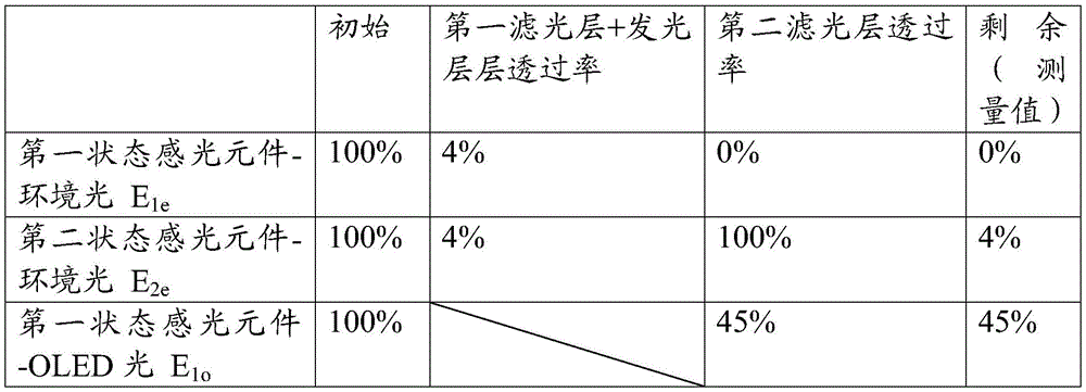

假设第一状态下,感光元件40的照度值为E1,由到达感光元件40的环境光E1e和OLED自发光E1o构成;同理,第二状态下,感光元件40的照度值为E2,由到达感光元件40的环境光E2e和OLED自发光E2o构成。Assuming that in the first state, the illuminance value of the
E1和E2通过感光元件40读取获得,Ee和Eo是希望获得的数据。此时我们可以通过简单的关系得到Ee和Eo。E1 and E2 are obtained by reading the
E1=E1e+E1O=0+EO*45%;E 1 =E 1e +E 1O =0+E O *45%;
E2=E2e+E2O=Ee*4%+EO*100%;E 2 =E 2e +E 2O =E e *4%+E O *100%;
求解得到,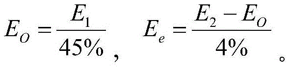
需要说明的是,作为一种可选的实施方式,所述感光元件40包括光敏传感器、红外传感器、指纹传感器和摄像头模组中的至少一项。这样,增加了感光元件40的多样性,同时,还增加了电子设备的智能化程度。It should be noted that, as an optional implementation manner, the
其中,当感光元件40包括光敏传感器,且在计算得到上述外部环境中的第二光线的数值的情况下,电子设备的控制器可以控制电子设备内的其他部件执行目标操作,上述目标操作可以包括以下至少一种:调节显示屏的显示亮度、调节显示屏的对比度和调节显示屏的背光颜色。Wherein, when the
当感光元件40包括红外传感器,且在计算得到上述外部环境中的第二光线的数值的情况下,上述第二光线可以为发光层20发出、且投射出显示屏遇到障碍物返回的反射红外光,这样,在计算得到上述第二光线的数值时,可以根据该数值确定障碍物与电子设备之间的距离,并根据该距离确定显示屏的状态为亮屏状态或灭屏状态。When the
当感光元件40包括指纹传感器或者摄像头模组的情况下,可以在第一状态或者第二状态的情况下获取图像。例如:当在第一状态的情况下获取图像,由于此时只有第一光线传输至感光元件40中,从而减小了外部环境中的第二光线对成像质量的影响;当在第二状态下获取图像,由于此时第一光线和第二光线均可以传输至感光元件40中,从而增强了获取的图像的显示亮度。When the
其中,作为一种可选的实施方式,所述电子设备还包括印制电路板50,所述感光元件40设置于所述印制电路板50上。这样,可以通过印制电路板50对感光元件40实现供电,同时印制电路板50还可以对感光元件40起到支撑作用。Wherein, as an optional implementation manner, the electronic device further includes a printed
需要说明的是,当电子设备中设置有第一套筒84和第二套筒83时(具体可以参见下文中的相应表述,在此不再赘述),第一套筒84和第二套筒83也可以设置于印制电路板50上,感光元件40可以设置于第二套筒83内,同时,感光元件40与印制电路板50电连接。这样,同样可以对第一套筒84和第二套筒83起到支撑作用。It should be noted that when the electronic device is provided with the
其中,第一滤光层10和第二滤光层30的具体结构在此不做限定,第一滤光层10和第二滤光层30均用于改变光线的偏振方向。Wherein, the specific structures of the
另外,参见图1,电子设备还可以包括透光盖板60,透光盖板60与第一滤光层10背离发光层20的表面抵接,从而可以实现对第一滤光层10的保护。In addition, referring to FIG. 1 , the electronic device may further include a light-transmitting
作为一种可选的实施方式,参见图1,所述第一滤光层10包括第一线偏振片11和第一1/4玻片12,所述第一1/4波片12设置于所述第一线偏振片11和所述发光层20之间。As an optional implementation manner, referring to FIG. 1, the
作为一种可选的实施方式,参见图1,所述第二滤光层30包括第二线偏振片32和第二1/4玻片31,所述第二1/4波片31设置于所述第二线偏振片32和所述发光层20之间。As an optional implementation manner, referring to FIG. 1, the
本申请实施方式中,由于第一滤光层10包括第一线偏振片11和第一1/4玻片12,第二滤光层30包括第二线偏振片32和第二1/4玻片31,在对光线实现过滤的基础上,可以降低使用成本,简化装配过程。In the embodiment of the present application, since the
其中,第一1/4玻片12和第二1/4玻片31可以分别被称作为为1/4波片或者1/4λ波片,而第一滤光层10的偏振方向可以指的是第一线偏振片11的偏振方向,第二滤光层30的偏振方向可以指的是第二线偏振片32的偏振方向。例如:参见图2,第一线偏振片11的偏振方向可以为X方向或者Y方向,相应的,第二线偏振片32的偏振方向也可以为X方向或者Y方向。Wherein, the first 1/4 glass slide 12 and the second 1/4 glass slide 31 can be referred to as 1/4 wave plate or 1/4λ wave plate respectively, and the polarization direction of the
其中,作为一种可选的实施方式,第一线偏振片11和第一1/4玻片12之间可以层叠设置,第二线偏振片32和第二1/4玻片31之间可以层叠设置;作为另一种可选的实施方式,第一线偏振片11和第一1/4玻片12之间可以间隔设置,第二线偏振片32和第二1/4玻片31之间可以间隔设置。例如:第一线偏振片11和第一1/4波片12之间可以通过粘接层间隔设置,或者,第一线偏振片11和第一1/4玻片12之间可以具有间隙,相应的,第二线偏振片32和第二1/4玻片31之间的位置关系可以参见上述第一线偏振片11和第一1/4玻片12的相关表述,在此不再赘述。Wherein, as an optional embodiment, the first linear polarizing plate 11 and the first 1/4 glass plate 12 can be stacked, and the second linear polarizing plate 32 and the second 1/4 glass plate 31 can be stacked Setting; As another optional embodiment, the first linear polarizing plate 11 and the first 1/4 glass plate 12 can be spaced apart, and the second linear polarizing plate 32 and the second 1/4 glass plate 31 can be interval setting. For example: the first linear polarizer 11 and the first 1/4 wave plate 12 can be arranged at intervals through an adhesive layer, or there can be a gap between the first linear polarizer 11 and the first 1/4 glass plate 12, Correspondingly, the positional relationship between the second linear polarizer 32 and the second 1/4 glass slide 31 can refer to the relevant descriptions of the above-mentioned first linear polarizer 11 and the first 1/4 glass slide 12 , which will not be repeated here.
其中,发光层20的具体类型在此不做限定,作为一种可选的实施方式,所述发光层20为有机发光二极管(Organic Light-Emitting Diode,OLED)发光层。这样,可以使得发光层20的发光效果较好。Wherein, the specific type of the light-emitting
需要说明的是,当发光层20为OLED发光层时,发光层20与第一滤光层10可以组合形成显示模组的一部分,即发光层与第一滤光层10可以构成OLED显示模组的两部分。It should be noted that when the light-emitting
作为一种可选的实施方式,参见图1,所述发光层20和所述第二滤光层30之间还设置有遮光层70,所述遮光层70与所述第二滤光层30相对的位置上开设有透光孔71。这样,由于遮光层70上未开设有透光孔71的位置可以对光线起到遮光作用。进一步降低了其他光线对感光元件40的探测结果的准确度的影响,即进一步提高了感光元件40的探测结果的准确度。As an optional implementation manner, referring to FIG. 1 , a light-
其中,遮光层70的具体材料在此不做限定,例如:遮光层70可以为遮光泡棉层,这样,降低了使用成本,还可以在发光层20与第二滤光层30之间起到缓冲作用。另外,遮光层70还可以为遮光橡胶层或者遮光镀层等。Wherein, the specific material of the light-
可选地,参见图1和图2,所述驱动组件80包括动力件81、传动件82、第一套筒84和第二套筒83,所述第一套筒84套设于所述第二套筒83上,所述动力件81通过所述传动件82与所述第一套筒84连接,且通过所述传动件82驱动所述第一套筒84围绕所述第二套筒83转动,所述感光元件40设置于所述第二套筒83内,所述第二滤光层30设置于所述第一套筒84上。Optionally, referring to FIG. 1 and FIG. 2, the driving
其中,第二滤光层30可以设置在第一套筒84朝向发光层20的端面上。Wherein, the
这样,由于感光元件40设置于第二套筒83内,从而增强对感光元件40的固定效果,以及对第二滤光层30的支撑效果。In this way, since the
其中,第一套筒84和第二套筒83可以为圆筒状支架。另外,第一套筒84和第二套筒83的材质在此也不做限定,例如:第一套筒84和第二套筒83可以为金属支架或者绝缘支架等。Wherein, the
可选地,参见图2,传动件82为传动齿轮,且所述传动齿轮套设于所述第一套筒84上,所述传动齿轮与所述第一套筒84固定连接。这样,增大了传动齿轮与第一套筒84的连接面,从而增强了对第一套筒84的传动效果。Optionally, referring to FIG. 2 , the
其中,动力件81可以为驱动马达,当然,驱动马达也可以被称作为驱动电机。另外,传动件82也可以为齿轮组。或者,传动件82也可以为传输轴与传动齿轮的组合。具体方式在此不做限定,从而增强了驱动组件80的多样性和灵活性。Wherein, the
其中,作为一种可选的实施方式,所述第二套筒83的外壁上设置有限位部。这样,由于第二套筒83的外壁上设置有限位部,从而可以防止第一套筒84沿着第二套筒83的轴向方向滑动,进而增强了对第一套筒84的限位作用,即使得第一套筒84在限位部所在的一侧区域内围绕第二套筒83转动。Wherein, as an optional implementation manner, a limiting portion is provided on the outer wall of the
本申请实施例还提供一种电子设备,包括上述实施例中的显示模组,由于本申请实施例提供的电子设备包括上述实施例中的显示模组,因而具有与上述实施例相同的有益技术效果,而显示模组的结构可以参见上述实施例中的相应表述,具体在此不再赘述。The embodiment of the present application also provides an electronic device, including the display module in the above-mentioned embodiment. Since the electronic device provided in the embodiment of the present application includes the display module in the above-mentioned embodiment, it has the same beneficial technology as the above-mentioned embodiment. effect, and the structure of the display module can refer to the corresponding expressions in the above-mentioned embodiments, and details will not be repeated here.
上面结合附图对本申请的实施例进行了描述,但是本申请并不局限于上述的具体实施方式,上述的具体实施方式仅仅是示意性的,而不是限制性的,本领域的普通技术人员在本申请的启示下,在不脱离本申请宗旨和权利要求所保护的范围情况下,还可做出很多形式,均属于本申请的保护之内。The embodiments of the present application have been described above in conjunction with the accompanying drawings, but the present application is not limited to the above-mentioned specific implementations. The above-mentioned specific implementations are only illustrative and not restrictive. Those of ordinary skill in the art will Under the inspiration of this application, without departing from the purpose of this application and the scope of protection of the claims, many forms can also be made, all of which belong to the protection of this application.
Claims (10)
Priority Applications (6)
| Application Number | Priority Date | Filing Date | Title |
|---|---|---|---|
| CN202010778799.2A CN111933665B (en) | 2020-08-05 | 2020-08-05 | Display module and electronic equipment |
| KR1020237006682A KR20230043186A (en) | 2020-08-05 | 2021-08-04 | Display module and electronic device |
| JP2023507353A JP7383200B2 (en) | 2020-08-05 | 2021-08-04 | Display module and electronic equipment |
| PCT/CN2021/110519 WO2022028471A1 (en) | 2020-08-05 | 2021-08-04 | Display module and electronic device |
| EP21854270.2A EP4195284A4 (en) | 2020-08-05 | 2021-08-04 | Display module and electronic device |
| US18/105,439 US20230189622A1 (en) | 2020-08-05 | 2023-02-03 | Display Module and Electronic Device |
Applications Claiming Priority (1)
| Application Number | Priority Date | Filing Date | Title |
|---|---|---|---|
| CN202010778799.2A CN111933665B (en) | 2020-08-05 | 2020-08-05 | Display module and electronic equipment |
Publications (2)
| Publication Number | Publication Date |
|---|---|
| CN111933665A CN111933665A (en) | 2020-11-13 |
| CN111933665B true CN111933665B (en) | 2023-04-07 |
Family
ID=73306468
Family Applications (1)
| Application Number | Title | Priority Date | Filing Date |
|---|---|---|---|
| CN202010778799.2A Active CN111933665B (en) | 2020-08-05 | 2020-08-05 | Display module and electronic equipment |
Country Status (6)
| Country | Link |
|---|---|
| US (1) | US20230189622A1 (en) |
| EP (1) | EP4195284A4 (en) |
| JP (1) | JP7383200B2 (en) |
| KR (1) | KR20230043186A (en) |
| CN (1) | CN111933665B (en) |
| WO (1) | WO2022028471A1 (en) |
Families Citing this family (3)
| Publication number | Priority date | Publication date | Assignee | Title |
|---|---|---|---|---|
| CN111933665B (en) * | 2020-08-05 | 2023-04-07 | 维沃移动通信有限公司 | Display module and electronic equipment |
| US12433024B2 (en) | 2022-05-18 | 2025-09-30 | Wuhan China Star Optoelectronics Technology Co., Ltd. | Array substrate and preparation method thereof, and display panel |
| CN114864605B (en) * | 2022-05-18 | 2025-09-23 | 武汉华星光电技术有限公司 | Array substrate and manufacturing method thereof, and display panel |
Citations (9)
| Publication number | Priority date | Publication date | Assignee | Title |
|---|---|---|---|---|
| WO2003071345A1 (en) * | 2002-02-20 | 2003-08-28 | Planar Systems, Nc. | Light sensitive display |
| JP2004184491A (en) * | 2002-11-29 | 2004-07-02 | Seiko Epson Corp | Display device and electronic device having the same |
| CN102498421A (en) * | 2009-09-14 | 2012-06-13 | 富士胶片株式会社 | Color filter and light-emitting display element |
| CN202856862U (en) * | 2012-10-23 | 2013-04-03 | 郭亚楠 | Infrared camera preventing infrared lamp from twinkling |
| TWI579675B (en) * | 2016-04-01 | 2017-04-21 | 英濟股份有限公司 | Laser dimming system |
| CN108347503A (en) * | 2018-01-29 | 2018-07-31 | 维沃移动通信有限公司 | A kind of terminal device and its control method |
| CN108449531A (en) * | 2018-03-26 | 2018-08-24 | 京东方科技集团股份有限公司 | Suspension touch camera module, electronic device and touch method |
| CN109036163A (en) * | 2018-08-31 | 2018-12-18 | 京东方科技集团股份有限公司 | A kind of display device and its environment light detection method |
| CN111366242A (en) * | 2020-05-27 | 2020-07-03 | 北京小米移动软件有限公司 | Ambient light detection device and terminal device |
Family Cites Families (12)
| Publication number | Priority date | Publication date | Assignee | Title |
|---|---|---|---|---|
| US9612152B2 (en) | 2013-11-07 | 2017-04-04 | Apple Inc. | Ambient light sensor with internal light cancellation |
| US9444075B2 (en) * | 2014-11-26 | 2016-09-13 | Universal Display Corporation | Emissive display with photo-switchable polarization |
| CN107241467B (en) | 2017-05-11 | 2020-08-07 | Oppo广东移动通信有限公司 | Electronic device |
| CN114353937A (en) * | 2017-08-22 | 2022-04-15 | 华为技术有限公司 | Optical sensor and terminal equipment |
| US11073712B2 (en) | 2018-04-10 | 2021-07-27 | Apple Inc. | Electronic device display for through-display imaging |
| CN108881538B (en) | 2018-06-22 | 2024-08-02 | 北京小米移动软件有限公司 | Mobile terminal |
| CN109411519A (en) * | 2018-10-23 | 2019-03-01 | 云谷(固安)科技有限公司 | Display panel and preparation method thereof, display device |
| CN112639800A (en) | 2018-12-18 | 2021-04-09 | 深圳市柔宇科技股份有限公司 | OLED screen body, fingerprint identification module and terminal equipment |
| CN110049214B (en) * | 2019-03-25 | 2024-06-14 | 华为技术有限公司 | Camera components and electronic equipment |
| CN110265442B (en) * | 2019-06-14 | 2021-04-02 | 京东方科技集团股份有限公司 | Display substrate and display panel including the same |
| CN110764301A (en) | 2019-10-31 | 2020-02-07 | Oppo广东移动通信有限公司 | Electronic device |
| CN111933665B (en) * | 2020-08-05 | 2023-04-07 | 维沃移动通信有限公司 | Display module and electronic equipment |
-
2020
- 2020-08-05 CN CN202010778799.2A patent/CN111933665B/en active Active
-
2021
- 2021-08-04 WO PCT/CN2021/110519 patent/WO2022028471A1/en not_active Ceased
- 2021-08-04 JP JP2023507353A patent/JP7383200B2/en active Active
- 2021-08-04 KR KR1020237006682A patent/KR20230043186A/en active Pending
- 2021-08-04 EP EP21854270.2A patent/EP4195284A4/en active Pending
-
2023
- 2023-02-03 US US18/105,439 patent/US20230189622A1/en active Pending
Patent Citations (9)
| Publication number | Priority date | Publication date | Assignee | Title |
|---|---|---|---|---|
| WO2003071345A1 (en) * | 2002-02-20 | 2003-08-28 | Planar Systems, Nc. | Light sensitive display |
| JP2004184491A (en) * | 2002-11-29 | 2004-07-02 | Seiko Epson Corp | Display device and electronic device having the same |
| CN102498421A (en) * | 2009-09-14 | 2012-06-13 | 富士胶片株式会社 | Color filter and light-emitting display element |
| CN202856862U (en) * | 2012-10-23 | 2013-04-03 | 郭亚楠 | Infrared camera preventing infrared lamp from twinkling |
| TWI579675B (en) * | 2016-04-01 | 2017-04-21 | 英濟股份有限公司 | Laser dimming system |
| CN108347503A (en) * | 2018-01-29 | 2018-07-31 | 维沃移动通信有限公司 | A kind of terminal device and its control method |
| CN108449531A (en) * | 2018-03-26 | 2018-08-24 | 京东方科技集团股份有限公司 | Suspension touch camera module, electronic device and touch method |
| CN109036163A (en) * | 2018-08-31 | 2018-12-18 | 京东方科技集团股份有限公司 | A kind of display device and its environment light detection method |
| CN111366242A (en) * | 2020-05-27 | 2020-07-03 | 北京小米移动软件有限公司 | Ambient light detection device and terminal device |
Also Published As
| Publication number | Publication date |
|---|---|
| US20230189622A1 (en) | 2023-06-15 |
| KR20230043186A (en) | 2023-03-30 |
| EP4195284A4 (en) | 2024-01-24 |
| JP7383200B2 (en) | 2023-11-17 |
| WO2022028471A1 (en) | 2022-02-10 |
| EP4195284A1 (en) | 2023-06-14 |
| CN111933665A (en) | 2020-11-13 |
| JP2023537704A (en) | 2023-09-05 |
Similar Documents
| Publication | Publication Date | Title |
|---|---|---|
| US12150339B2 (en) | Electronic devices with light sensors and displays | |
| CN111933665B (en) | Display module and electronic equipment | |
| US9013613B2 (en) | Sensor-equipped display apparatus and electronic apparatus | |
| TWI574194B (en) | Photographic module and optical touch screen using the same | |
| US9024250B2 (en) | Electronic device with light sensor alignment structures | |
| US11930686B2 (en) | Electronic device including camera module | |
| TWI580269B (en) | Photographic module and optical touch screen using the same | |
| CN101447145A (en) | Display device and electronic apparatus | |
| KR20210060186A (en) | Electronic device including camera device and display | |
| TWI578208B (en) | Optical touch screen | |
| CN115867961A (en) | Electronic device comprising a display | |
| US11569290B2 (en) | Sensing device and display apparatus including the same | |
| CN106453724A (en) | Panel, sensor assembly and mobile terminal | |
| CN116893759A (en) | electronic device | |
| TWI578209B (en) | Camera module and optical touch screen using the same | |
| TWI559193B (en) | Optical touch screens | |
| CN206930977U (en) | Sensor cluster, cover plate assembly and mobile terminal | |
| CN111308782B (en) | Electronic equipment | |
| KR20240055216A (en) | Display device | |
| KR102174008B1 (en) | Electrode sheet and touch input device | |
| JP2013157372A (en) | Optical sensor device, and manufacturing method of the same | |
| CN103713734A (en) | Miniaturized optical system, light source module and portable electronic device | |
| CN117694034A (en) | Electronic devices including cameras under displays and displays included in electronic devices | |
| KR20240164619A (en) | Display device | |
| KR20240034950A (en) | Display device |
Legal Events
| Date | Code | Title | Description |
|---|---|---|---|
| PB01 | Publication | ||
| PB01 | Publication | ||
| SE01 | Entry into force of request for substantive examination | ||
| SE01 | Entry into force of request for substantive examination | ||
| GR01 | Patent grant | ||
| GR01 | Patent grant |