CN111897512A - Configurable multi-port FIFO memory - Google Patents
Configurable multi-port FIFO memory Download PDFInfo
- Publication number
- CN111897512A CN111897512A CN202010735155.5A CN202010735155A CN111897512A CN 111897512 A CN111897512 A CN 111897512A CN 202010735155 A CN202010735155 A CN 202010735155A CN 111897512 A CN111897512 A CN 111897512A
- Authority
- CN
- China
- Prior art keywords
- read
- write
- sub
- port
- selector
- Prior art date
- Legal status (The legal status is an assumption and is not a legal conclusion. Google has not performed a legal analysis and makes no representation as to the accuracy of the status listed.)
- Pending
Links
Images


Classifications
-
- G—PHYSICS
- G06—COMPUTING OR CALCULATING; COUNTING
- G06F—ELECTRIC DIGITAL DATA PROCESSING
- G06F5/00—Methods or arrangements for data conversion without changing the order or content of the data handled
- G06F5/06—Methods or arrangements for data conversion without changing the order or content of the data handled for changing the speed of data flow, i.e. speed regularising or timing, e.g. delay lines, FIFO buffers; over- or underrun control therefor
Landscapes
- Engineering & Computer Science (AREA)
- Theoretical Computer Science (AREA)
- Physics & Mathematics (AREA)
- General Engineering & Computer Science (AREA)
- General Physics & Mathematics (AREA)
- Static Random-Access Memory (AREA)
Abstract
本公开的实施例公开了可配置多端口的FIFO存储器。该存储器的一具体实施方式包括:多个读端口和写端口;存储体分为多个子存储体;每个子存储体的一端与多个写端口连接,每个子存储体的另一端与多个读端口连接;多个写入选择器组件中的每个写入选择器组件设置到一个写端口和存储体之间,写入选择器组件用于确定数据写入的子存储体;多个读取选择器组件中的每个读取选择器组件设置到一个读端口和存储体之间,读取选择器组件用于确定数据读取的子存储体。该实施方式通过将存储体划分为多个子存储体,以及用过上述写入选择器组件和读取选择器组件确定写入和读取数据的子存储体。进而可以实现存储体的充分利用,避免了存储体的资源浪费。
Embodiments of the present disclosure disclose a configurable multi-port FIFO memory. A specific implementation of the memory includes: a plurality of read ports and write ports; a memory bank is divided into a plurality of sub memory banks; one end of each sub memory bank is connected to a plurality of write ports, and the other end of each sub memory bank is connected to a plurality of read ports Port connection; each write selector assembly in the plurality of write selector assemblies is set between a write port and a bank, and the write selector assembly is used to determine the sub-bank to which data is written; multiple reads Each read selector assembly in the selector assemblies is arranged between a read port and a memory bank, and the read selector assembly is used to determine the sub memory bank from which data is read. This embodiment determines the sub-banks to which data is written and read by dividing the bank into a plurality of sub-banks, and using the above-described write selector component and read selector component. Further, full utilization of the storage body can be achieved, and resource waste of the storage body can be avoided.
Description
技术领域technical field
本公开的实施例涉及集成电路设计领域,具体涉及可配置多端口的FIFO存储器。Embodiments of the present disclosure relate to the field of integrated circuit design, and in particular, to a configurable multi-port FIFO memory.
背景技术Background technique
FIFO存储器(First Input First Output)是先进先出的双口缓冲器。上述FIFO存储器通常用于数据缓冲,以平抑短时间内数据发送端和接收端处理能力差的问题。FIFO memory (First Input First Output) is a first-in, first-out dual-port buffer. The above-mentioned FIFO memory is usually used for data buffering, so as to alleviate the problem of poor processing capability of the data sending end and the receiving end in a short time.
对于多路数据传输系统的情况下,需要配置数量相匹配的数据传输通道,同时在每个上述数据传输通道配置与数据的规格相匹配容量的FIFO存储器以平抑数据传输带来的溢出风险。In the case of a multiplexed data transmission system, it is necessary to configure a matching number of data transmission channels, and at the same time configure a FIFO memory with a capacity matching the data specifications in each of the above data transmission channels to reduce the risk of overflow caused by data transmission.
但是,在实际工况中,一些数据传输通道并非持续工作,从而导致部分FIFO存储器闲置。进而不能使FIFO存储器的存储资源被充分利用,造成了资源浪费,也增加了系统的成本。However, in actual working conditions, some data transmission channels do not work continuously, which results in part of the FIFO memory being idle. Furthermore, the storage resources of the FIFO memory cannot be fully utilized, resulting in a waste of resources and an increase in the cost of the system.
相应地,本领域需要一种新的FIFO存储器来解决上述问题。Accordingly, there is a need in the art for a new FIFO memory to solve the above problems.
发明内容SUMMARY OF THE INVENTION
本公开的内容部分用于以简要的形式介绍构思,这些构思将在后面的具体实施方式部分被详细描述。本公开的内容部分并不旨在标识要求保护的技术方案的关键特征或必要特征,也不旨在用于限制所要求的保护的技术方案的范围。This summary of the disclosure serves to introduce concepts in a simplified form that are described in detail in the detailed description that follows. The content section of this disclosure is not intended to identify key features or essential features of the claimed technical solution, nor is it intended to be used to limit the scope of the claimed technical solution.
为了解决上述问题,即相关的多路数据传输系统的FIFO存储器存在存储资源不能被充分利用,增加上述系统的成本等问题,本公开的一些实施例提出了可配置多端口的FIFO存储器,包括:多个读端口和写端口;存储体,上述存储体分为多个子存储体;每个上述子存储体的一端与上述多个写端口连接,每个上述子存储体的另一端与上述多个读端口连接;与上述写端口数量相匹配的多个写入选择器组件,上述多个写入选择器组件中的每个写入选择器组件设置到一个写端口和上述存储体之间,上述写入选择器组件用于确定数据写入的子存储体;与上述读端口数量相匹配的多个读取选择器组件,上述多个读取选择器组件中的每个读取选择器组件设置到一个读端口和上述存储体之间,上述读取选择器组件用于确定数据读取的子存储体。In order to solve the above-mentioned problems, that is, the FIFO memory of the related multiplex data transmission system has the problems that the storage resources cannot be fully utilized, and the cost of the above-mentioned system is increased, some embodiments of the present disclosure propose a configurable multi-port FIFO memory, including: A plurality of read ports and write ports; a storage bank, the storage bank is divided into a plurality of sub storage banks; one end of each of the sub storage banks is connected to the plurality of write ports, and the other end of each of the sub storage banks is connected to the plurality of sub storage banks Read port connection; a plurality of write selector assemblies matching the number of the above write ports, each write selector assembly in the above plurality of write selector assemblies is arranged between a write port and the above-mentioned storage bank, the above The write selector component is used to determine the sub-storage bank to which the data is written; a plurality of read selector components matching the above-mentioned number of read ports, each read selector component in the above-mentioned plurality of read selector components is set Between a read port and the above-mentioned memory bank, the above-mentioned read selector component is used to determine the sub-memory bank from which data is read.
在一些实施例中,上述写入选择器组件包括写入模式控制器,上述写入模式控制器连接上述写端口和上述多个子存储体,上述写入模式控制器在上述写端口与每个上述子存储体之间形成多条写入路径,从而使该写端口的数据能够写入到多个上述子存储体。In some embodiments, the write selector assembly includes a write mode controller, the write mode controller is connected to the write port and the plurality of sub-banks, and the write mode controller is connected between the write port and each of the above A plurality of write paths are formed between the sub memory banks, so that the data of the write port can be written to a plurality of the above sub memory banks.
在一些实施例中,上述读取选择器组件包括读取模式控制器,上述读取模式控制器连接上述读端口和上述多个子存储体,上述读取模式控制器在读端口与上述每个子存储体之间形成多条读取路径,从而使该读端口可以读取多个上述子存储体中的数据。In some embodiments, the read selector assembly includes a read mode controller, the read mode controller is connected to the read port and the plurality of sub-banks, and the read mode controller is connected to each of the sub-banks between the read port and the sub-banks. A plurality of read paths are formed between them, so that the read port can read data in a plurality of the sub-memory banks.
在一些实施例中,上述写入选择器组件还包括写端口选择器,上述写端口选择器的一端与上述多个写入选择器组件的写入模式控制器连接,上述写端口选择器的另一端连接上述多个子存储体,上述写端口选择器用于确定有效的写端口,以及根据写指针范围与上述多个子存储体的地址空间选择对应的上述写入路径,进而将数据写入对应的子存储体。In some embodiments, the write selector assembly further includes a write port selector, one end of the write port selector is connected to the write mode controllers of the plurality of write selector assemblies, and the other end of the write port selector is connected to the write mode controllers of the plurality of write selector assemblies. One end is connected to the plurality of sub-memory banks, the write port selector is used to determine an effective write port, and select the corresponding write path according to the write pointer range and the address space of the plurality of sub-memory banks, and then write data into the corresponding sub-memory banks. memory bank.
在一些实施例中,上述FIFO存储器还包括与上述多个子存储体数量相匹配的写状态模块,响应于上述写状态模块检测到对应的子存储体的地址空间未满时,发送写使能信号到上述写入模式控制器,允许上述写端口进行写入操作;响应于上述写状态模块检测到对应的子存储体的地址空间已满时,发送使能信号,禁止上述写端口的数据写入到该子存储体,以及,响应于检测到下一子存储体的地址空间未满时,发送写使能信号,将上述写端口的数据写入到该子存储体。In some embodiments, the FIFO memory further includes a write status module matching the number of the plurality of sub-memory banks, and in response to the write status module detecting that the address space of the corresponding sub-memory bank is not full, it sends a write enable signal to the above-mentioned write mode controller, allowing the above-mentioned write port to perform a write operation; in response to the above-mentioned write status module detecting that the address space of the corresponding sub-memory bank is full, it sends an enable signal to prohibit the data writing of the above-mentioned write port to this sub-bank, and in response to detecting that the address space of the next sub-bank is not full, a write enable signal is sent to write the data of the above-mentioned write port to this sub-bank.
在一些实施例中,上述读取选择器组件包括读端口选择器,上述读端口选择器的一端与上述多个读取选择器组件的读取模式控制器连接,上述读端口选择器的另一端连接上述多个子存储体,上述读端口选择器用于确定有效的读端口,以及根据读指针选择对应的上述读取路径,进而读取对应的子存储体中的数据。In some embodiments, the read selector assembly includes a read port selector, one end of the read port selector is connected to the read mode controllers of the plurality of read selector assemblies, and the other end of the read port selector is connected to the read mode controller of the plurality of read selector assemblies. The plurality of sub-memory banks are connected, and the read port selector is used to determine an effective read port, and select the corresponding read path according to the read pointer, so as to read data in the corresponding sub-memory bank.
在一些实施例中,上述FIFO存储器还包括与上述多个子存储体数量相匹配的读状态模块,响应于上述读状态模块检测到对应的子存储体的地址空间未空时,发送读使能信号到上述读取模式控制器,允许上述读端口进行读取操作;响应于上述读状态模块检测到对应的子存储体的地址空间已空时,发送使能信号,禁止上述读端口读取该子存储体的数据,以及,响应于检测到下一子存储体的地址空间未空时,发送写使能信号,使上述读端口读取该存储体中的数据。In some embodiments, the FIFO memory further includes a read status module matching the number of the plurality of sub memory banks, and in response to the read status module detecting that the address space of the corresponding sub memory bank is not empty, it sends a read enable signal To the above-mentioned read mode controller, the above-mentioned read port is allowed to perform a read operation; in response to the above-mentioned read status module detecting that the address space of the corresponding sub-memory bank is empty, it sends an enable signal to prohibit the above-mentioned read port from reading the sub-memory bank. data of the memory bank, and, in response to detecting that the address space of the next sub-memory bank is not empty, send a write enable signal to cause the read port to read the data in the memory bank.
本公开的上述各个实施例中的一个实施例具有如下有益效果:通过将存储体划分为多个子存储体,以及用过上述写入选择器组件和读取选择器组件确定写入和读取数据的子存储体。进而可以实现存储体的充分利用,避免了存储体的资源浪费。One of the above-described various embodiments of the present disclosure has the following beneficial effects: by dividing a memory bank into a plurality of sub-memory banks, and using the above-described write selector component and read selector component to determine write and read data sub memory bank. Further, full utilization of the storage body can be achieved, and resource waste of the storage body can be avoided.
附图说明Description of drawings
结合附图并参考以下具体实施方式,本公开各实施例的上述和其他特征、优点及方面将变得更加明显。贯穿附图中,相同或相似的附图标记表示相同或相似的元素。应当理解附图是示意性的,原件和元素不一定按照比例绘制。The above and other features, advantages and aspects of various embodiments of the present disclosure will become more apparent when taken in conjunction with the accompanying drawings and with reference to the following detailed description. Throughout the drawings, the same or similar reference numbers refer to the same or similar elements. It should be understood that the drawings are schematic and that the originals and elements are not necessarily drawn to scale.
图1是根据本公开的可配置多端口的FIFO存储器的一些实施例的结构示意图;1 is a schematic structural diagram of some embodiments of a configurable multi-port FIFO memory according to the present disclosure;
图2是根据本公开的可配置多端口的FIFO存储器的一些实施例的电路结构图;2 is a circuit block diagram of some embodiments of a configurable multi-port FIFO memory according to the present disclosure;
图3是根据本公开的可配置多端口的FIFO存储器的另一些实施例的电路结构图。3 is a circuit block diagram of other embodiments of a configurable multi-port FIFO memory according to the present disclosure.
具体实施方式Detailed ways
下面将参照附图更详细地描述本公开的实施例。虽然附图中显示了本公开的某些实施例,然而应当理解的是,本公开可以通过各种形式来实现,而且不应该被解释为限于这里阐述的实施例。相反,提供这些实施例是为了更加透彻和完整地理解本公开。应当理解的是,本公开的附图及实施例仅用于示例性作用,并非用于限制本公开的保护范围。Embodiments of the present disclosure will be described in more detail below with reference to the accompanying drawings. While certain embodiments of the present disclosure are shown in the drawings, it should be understood that the present disclosure may be embodied in various forms and should not be construed as limited to the embodiments set forth herein. Rather, these embodiments are provided for a thorough and complete understanding of the present disclosure. It should be understood that the drawings and embodiments of the present disclosure are only for exemplary purposes, and are not intended to limit the protection scope of the present disclosure.
另外还需要说明的是,为了便于描述,附图中仅示出了与有关发明相关的部分。在不冲突的情况下,本公开中的实施例及实施例中的特征可以相互组合。In addition, it should be noted that, for the convenience of description, only the parts related to the related invention are shown in the drawings. The embodiments of this disclosure and features of the embodiments may be combined with each other without conflict.
需要注意,本公开中提及的“第一”、“第二”等概念仅用于对不同的装置、模块或单元进行区分,并非用于限定这些装置、模块或单元所执行的功能的顺序或者相互依存关系。It should be noted that concepts such as "first" and "second" mentioned in the present disclosure are only used to distinguish different devices, modules or units, and are not used to limit the order of functions performed by these devices, modules or units or interdependence.
需要注意,本公开中提及的“一个”、“多个”的修饰是示意性而非限制性的,本领域技术人员应当理解,除非在上下文另有明确指出,否则应该理解为“一个或多个”。It should be noted that the modifications of "a" and "a plurality" mentioned in the present disclosure are illustrative rather than restrictive, and those skilled in the art should understand that unless the context clearly indicates otherwise, they should be understood as "one or a plurality of". multiple".
本公开实施方式中的多个装置之间所交互的消息或者信息的名称仅用于说明性的目的,而并不是用于对这些消息或信息的范围进行限制。The names of messages or information exchanged between multiple devices in the embodiments of the present disclosure are only for illustrative purposes, and are not intended to limit the scope of these messages or information.
下面将参考附图并结合实施例来详细说明本公开。The present disclosure will be described in detail below with reference to the accompanying drawings and in conjunction with embodiments.
首先,请参见图1,图1是根据本公开的可配置多端口的FIFO存储器的一些实施例的结构示意图100。如图1所示,该可配置多端口的FIFO存储器包括多个写端口101、多个读端口105、写入选择器组件102、存储体103和读取选择器组件104。上述存储体103可以被分成与上述多个写端口101数量相匹配的子存储体。上述写入选择器组件102用于确定数据写入的子存储体。上述读取选择器组件104用于确定数据读取的子存储体。First, please refer to FIG. 1 , which is a schematic structural diagram 100 of some embodiments of a configurable multi-port FIFO memory according to the present disclosure. As shown in FIG. 1 , the configurable multi-port FIFO memory includes a plurality of
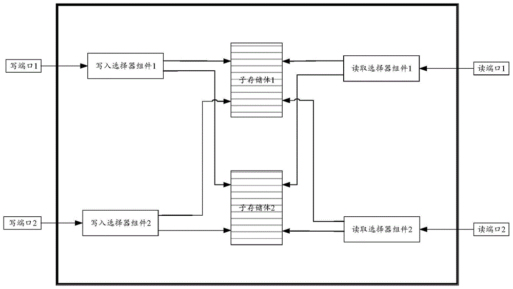
接着参阅图2,图2是根据本公开的可配置多端口的FIFO存储器的电路结构图。如图2所示,该可配置多端口的FIFO存储器包括写端口1、写端口2、读端口1、读端口2、子存储体1、子存储体2、两个写入选择器组件和两个读取选择器组件。具体而言,子存储体1的一端与写端口1和写端口2连接。子存储体1的另一端与读端口1和读端口2连接。写入选择器组件1的一端连接写端口1,另一端连接子存储体1和存储体2,上述写入选择器组件1用于确定写端口1的数据写入到子存储体1或者子存储体2。写入选择器组件2的一端连接到写端口2,另一端连接到子存储体1和子存储体2,上述写入选择器组件2用于确定写端口2的数据写入到子存储体1或者子存储体2。上述读取选择器组件1的两端分别连接读端口1和子存储体1与存储体2,上述读取选择器组件1用于确定读端口1从子存储体1或者子存储体2中读取数据。上述读取选择器组件2的两端分别连接读端口 2和子存储体1与子存储体2,上述读取选择器组件2用于确定读端口 2从子存储体1或者子存储体2中读取数据。Next, referring to FIG. 2 , FIG. 2 is a circuit structure diagram of a configurable multi-port FIFO memory according to the present disclosure. As shown in FIG. 2, the configurable multi-port FIFO memory includes write port 1, write port 2, read port 1, read port 2, sub-bank 1, sub-bank 2, two write selector components and two A read selector component. Specifically, one end of the sub-bank 1 is connected to the write port 1 and the write port 2 . The other end of the sub-bank 1 is connected to the read port 1 and the read port 2 . One end of the write selector assembly 1 is connected to the write port 1, and the other end is connected to the sub memory bank 1 and the memory bank 2. The above write selector assembly 1 is used to determine that the data of the write port 1 is written to the sub memory bank 1 or the sub memory bank. body 2. One end of the write selector component 2 is connected to the write port 2, and the other end is connected to the sub memory bank 1 and the sub memory bank 2. The above write selector component 2 is used to determine that the data of the write port 2 is written to the sub memory bank 1 or Subbank 2. The two ends of the read selector assembly 1 are respectively connected to the read port 1 and the sub memory bank 1 and the memory bank 2. The above read selector assembly 1 is used to determine that the read port 1 reads from the sub memory bank 1 or the sub memory bank 2. data. The two ends of the read selector assembly 2 are respectively connected to the read port 2 and the sub memory bank 1 and the sub memory bank 2. The above read selector assembly 2 is used to determine that the read port 2 reads from the sub memory bank 1 or the sub memory bank 2. fetch data.
需要说明的是,本领域技术人员可以根据读写端口的写入或者读取的数据的规格对子存储体1和子存储体2的容量。例如,写端口1 连接的数据传输通道传输的数据规格是1080P@30fps,写端口2连接的数据传输通道传输的数据规格是720P@30fps。那么可以将子存储体 1分配的容量高于子存储体2。再例如,写端口1连接的数据传输通道传输数据的次数高于写端口2,也可以将子存储体1分配的容量高于子存储体2。本领域技术人员可以根据实际情况对子存储体1和子存储体2的容量进行调整。It should be noted that those skilled in the art can adjust the capacities of the sub-memory bank 1 and the sub-memory bank 2 according to the specifications of the data written or read by the read-write port. For example, the data transmission specification of the data transmission channel connected to the write port 1 is 1080P@30fps, and the data transmission specification of the data transmission channel connected to the write port 2 is 720P@30fps. Then sub-bank 1 can be allocated a higher capacity than sub-bank 2. For another example, if the data transmission channel connected to the write port 1 transmits data more frequently than the write port 2, the sub-memory bank 1 may also be allocated a higher capacity than the sub-memory bank 2. Those skilled in the art can adjust the capacities of the sub-storage bank 1 and the sub-storage bank 2 according to the actual situation.
上述写入选择器组件1、写入选择器组件2可以是包括多条指令的寄存器。举例而言,上述指令可以包括:响应于写端口1和写端口 2有效,将写端口1的数据写入到子存储体1,写端口2的数据写入到子存储器2。此时,写端口1和子存储体1、写端口2和子存储体2 相当于两个独立的传统FIFO,彼此独立工作。The above-mentioned write selector component 1 and write selector component 2 may be registers including multiple instructions. For example, the above instruction may include: in response to the write port 1 and the write port 2 being valid, writing the data of the write port 1 to the sub-memory bank 1, and writing the data of the write port 2 to the sub-memory 2. At this time, the write port 1 and the sub-memory bank 1, and the write port 2 and the sub-memory bank 2 are equivalent to two independent traditional FIFOs, which work independently of each other.
上述指令还可以包括:响应于写端口1有效以及写端口2无效,将写端口1的数据写入到子存储体1和/或子存储体2中。此时,写端口1可以将数据写入到子存储体1和/或子存储体2中。如此一来,对于写端口1,子存储体1和子存储体2的组合相对于子存储体1而言,大幅度地增加了存储深度。更好地实现了对数据的缓冲功能。The above instruction may further include: in response to the write port 1 being valid and the write port 2 being invalid, writing the data of the write port 1 into the sub memory bank 1 and/or the sub memory bank 2. At this time, the write port 1 can write data into the sub-bank 1 and/or the sub-bank 2. In this way, for the write port 1, the combination of the sub-bank 1 and the sub-bank 2 greatly increases the storage depth relative to the sub-bank 1. Better implementation of data buffering.
同样地,上述读取选择器组件1、读取选择器组件2也可以是包括多条指令的寄存器。举例而言,上述指令可以包括:响应于读端口 1和读端口2有效,通过读端口1读取子存储体1中的数据,通过读端口2读取子存储器2中的数据。此时,读端口1和子存储体1、读端口2和子存储体2相当于两个独立的传统FIFO,彼此独立工作。Similarly, the read selector component 1 and the read selector component 2 described above may also be registers including multiple instructions. For example, the above-mentioned instruction may include: in response to the read port 1 and the read port 2 being valid, reading the data in the sub-memory bank 1 through the read port 1, and reading the data in the sub-memory bank 2 through the read port 2. At this time, read port 1 and sub-bank 1, read port 2 and sub-bank 2 are equivalent to two independent traditional FIFOs, and work independently of each other.
上述指令还可以包括:响应于读端口1有效以及读端口2无效,通过读端口1读取子存储体1和/或子存储体2中的数据。此时,读端口1可以读取子存储体1和/或子存储体2中的数据。如此一来,子存储体1和子存储体2的组合相对于子存储体1而言,大幅度地增加了存储深度。更好地实现了对数据的缓冲功能。The above instruction may further include: in response to the read port 1 being valid and the read port 2 being invalid, reading the data in the sub-bank 1 and/or the sub-bank 2 through the read port 1 . At this time, the read port 1 can read the data in the sub-bank 1 and/or the sub-bank 2. In this way, the combination of the sub-memory bank 1 and the sub-memory bank 2 greatly increases the storage depth compared to the sub-memory bank 1 . Better implementation of data buffering.
在一些实施例的一些可选实现方式中,上述写入选择器组件可以包括写入模式控制器和写端口选择器。上述读取选择器组件可以包括读取模式控制器和读端口选择器。接下来结合图3进行说明。图3是根据本公开的可配置多端口的FIFO存储器的另一些实施例的电路结构图。如图3所示,上述写入选择器组件1可以包括写入模式控制器 1和写端口选择器1。上述写入模式控制器1在写端口1与子存储体1 和子存储体2之间形成两条读取路径。In some alternative implementations of some embodiments, the write selector component described above may include a write mode controller and a write port selector. The read selector assembly described above may include a read mode controller and a read port selector. Next, description will be given with reference to FIG. 3 . 3 is a circuit block diagram of other embodiments of a configurable multi-port FIFO memory according to the present disclosure. As shown in FIG. 3 , the above-mentioned write selector assembly 1 may include a write mode controller 1 and a write port selector 1. The above-mentioned write mode controller 1 forms two read paths between the write port 1 and the sub-bank 1 and the sub-bank 2 .
上述写入模式控制器1的一端与写端口1连接,另一端与写端口选择器1和写端口选择器2的一端连接。上述写端口选择器1的另一端与子存储体1和子存储体2连接。One end of the above-mentioned write mode controller 1 is connected to the write port 1 , and the other end is connected to one end of the write port selector 1 and the write port selector 2 . The other end of the above-mentioned write port selector 1 is connected to the sub-bank 1 and the sub-bank 2 .
上述写入模式控制器2的一端与写端口2连接,另一端与写端口选择器1和写端口选择器2的一端连接。上述写端口选择器2的另一端与子存储体1和子存储体2连接。One end of the above-mentioned write mode controller 2 is connected to the write port 2 , and the other end is connected to one end of the write port selector 1 and the write port selector 2 . The other end of the above-mentioned write port selector 2 is connected to the sub-bank 1 and the sub-bank 2 .
上述写入模式控制器1和写入模式控制器2可以是包括多条指令的寄存器。上述指令指代多种选择模式,例如单端口写入模式和双端口写入模式等。技术人员可以通过向写端口选择器中输入控制码选择上述选择模式,进而选择单端口写入模式或者双端口写入模式。从而实现了该FIFO存储器对多端口的灵活选择。The above-mentioned write mode controller 1 and write mode controller 2 may be registers including a plurality of instructions. The above commands refer to various selection modes, such as single-port write mode and dual-port write mode. A technician can select the above selection mode by inputting a control code into the write port selector, and then select a single port write mode or a dual port write mode. Thus, the flexible selection of the FIFO memory for multiple ports is realized.
上述写端口选择器1也可以对上述两条写入路径进行选择。该写端口选择器1可以是数据选择器。具体而言,写端口选择器1可以根据写指针范围与上述两个子存储体的地址空间选择对应的上述写入路径,进而将数据写入对应的子存储体。举例来说,写端口1可以使用子存储体1中0-7的地址空间。写端口1还可以使用子存储体2中8-15 的地址空间。上述写端口选择器1可以获取到写端口1的指针范围,进而确定该数据写入到子存储体1还是子存储体2。进一步地,上述写端口选择器1还可以根据上述写端口1和写端口2是否有效选择写入路径。响应于写端口1和写端口2均有效,上述写端口1的数据优先写入子存储体1中0-7的地址空间。响应于写端口1有效,写端口2 无效,上述写端口1的数据可以根据子存储体1和子存储体2的容量选择写入子存储体1中0-7的地址空间以及子存储体2中8-15的地址空间。The above-mentioned write port selector 1 can also select the above-mentioned two write paths. The write port selector 1 may be a data selector. Specifically, the write port selector 1 can select the corresponding write path according to the write pointer range and the address space of the two sub-memory banks, and then write data into the corresponding sub-memory bank. For example, write port 1 may use the address space 0-7 in subbank 1. Write port 1 can also use the address space 8-15 in subbank 2. The above-mentioned write port selector 1 can obtain the pointer range of the write port 1, and then determine whether the data is written to the sub-memory bank 1 or the sub-memory bank 2. Further, the above-mentioned write port selector 1 may also select a write path according to whether the above-mentioned write port 1 and write port 2 are valid. In response to both the write port 1 and the write port 2 being valid, the data of the write port 1 is preferentially written into the address space of 0-7 in the sub-memory bank 1 . In response to the write port 1 being valid and the write port 2 being invalid, the data of the write port 1 can be selectively written to the address space 0-7 in the sub memory bank 1 and the sub memory bank 2 according to the capacity of the sub memory bank 1 and the sub memory bank 2. 8-15 address space.
进一步地,上述FIFO存储器还包括与上述两个子存储体数量相匹配的写状态模块(图中未示出)。响应于上述写状态模块检测到子存储体1或者子存储体2的地址空间未满时,发送写使能信号到上述写入模式控制器1,允许上述写端口1进行写入操作;响应于上述写状态模块检测到对应的子存储体的地址空间已满时,发送使能信号,禁止上述写端口1的数据写入到子存储体1,以及,响应于检测到子存储体2的地址空间未满时,发送写使能信号,将上述写端口1的数据写入到子存储体2。Further, the above-mentioned FIFO memory further includes a write status module (not shown in the figure) matching the number of the above-mentioned two sub-memory banks. In response to the above-mentioned write status module detecting that the address space of sub-memory bank 1 or sub-memory bank 2 is not full, it sends a write enable signal to the above-mentioned write mode controller 1 to allow the above-mentioned write port 1 to perform a write operation; in response to When the above-mentioned write status module detects that the address space of the corresponding sub-memory bank is full, it sends an enable signal to prohibit the data of the above-mentioned write port 1 from being written to the sub-memory bank 1, and, in response to detecting the address of the sub-memory bank 2 When the space is not full, a write enable signal is sent to write the data of the above write port 1 to the sub memory bank 2.
如此一来,通过配置不同数量的写端口和读端口,可以大幅度地增加存储深度。更好地实现了对多路数据的缓冲功能。In this way, the memory depth can be greatly increased by configuring different numbers of write ports and read ports. Better realize the buffering function of multi-channel data.
接着参阅图3,如图3所示,以读取选择器组件1为例进行说明。上述读取选择器组件1可以包括读取模式控制器1和读端口选择器1。上述读取模式控制器1在读端口1与子存储体1和子存储体2之间形成两条读取路径。Next, referring to FIG. 3 , as shown in FIG. 3 , the reading selector assembly 1 is taken as an example for description. The read selector assembly 1 described above may include a read mode controller 1 and a read port selector 1 . The read mode controller 1 described above forms two read paths between the read port 1 and the sub-bank 1 and the sub-bank 2 .
上述读取模式控制器1的一端与读端口1连接,另一端与读端口选择器1和读端口选择器2的一端连接。上述读端口选择器1的另一端与子存储体1和子存储体2连接。One end of the read mode controller 1 is connected to the read port 1 , and the other end is connected to one end of the read port selector 1 and the read port selector 2 . The other end of the read port selector 1 is connected to the sub memory bank 1 and the sub memory bank 2 .
上述读取模式控制器2的一端与读端口2连接,另一端与读端口选择器1和读端口选择器2的一端连接。上述读端口选择器2的另一端与子存储体1和子存储体2连接。One end of the read mode controller 2 is connected to the read port 2 , and the other end is connected to one end of the read port selector 1 and the read port selector 2 . The other end of the read port selector 2 is connected to the sub memory bank 1 and the sub memory bank 2 .
上述读取模式控制器1和读取模式控制器2可以是包括多条指令的寄存器。上述指令指代多种选择模式,例如单端口读取模式和双端口读取模式等。技术人员可以通过向读端口选择器中输入控制码选择上述选择模式,进而选择单端口读取模式或者双端口读取模式。从而实现了该FIFO存储器对多端口的灵活选择。The read mode controller 1 and the read mode controller 2 described above may be registers including a plurality of instructions. The above commands refer to various selection modes, such as single-port read mode and dual-port read mode. A technician can select the above selection mode by inputting a control code into the read port selector, and then select a single port read mode or a dual port read mode. Thus, the flexible selection of the FIFO memory for multiple ports is realized.
上述读端口选择器1也可以对上述两条写入路径进行选择。该读端口选择器可以是数据选择器。具体而言,读端口选择器1可以根据读指针范围与上述两个子存储体的地址空间选择对应的上述读取路径,进而读取对应的子存储体中的数据。举例来说,读端口1可以读取子存储体1中0-7的地址空间。读端口1还可以读取子存储体2中 8-15的地址空间。上述读端口选择器可以获取到读端口1的指针范围,进而确定读取子存储体1还是子存储体2中的数据。进一步地,上述读端口选择器1还可以根据上述读端口1和读端口2是否有效选择读取路径。响应于读端口1和读端口2均有效,上述读端口1优先读取子存储体1中0-7的地址空间。响应于读端口1有效,读端口2无效,上述读端口1的数据可以根据子存储体1和子存储体2的容量选择读取子存储体1中0-7的地址空间以及子存储体2中8-15的地址空间。The above-mentioned read port selector 1 can also select the above-mentioned two write paths. The read port selector may be a data selector. Specifically, the read port selector 1 can select the corresponding read path according to the read pointer range and the address spaces of the two sub-memory banks, and then read the data in the corresponding sub-memory banks. For example, read port 1 can read the address space of 0-7 in subbank 1. Read port 1 can also read address space 8-15 in subbank 2. The above-mentioned read port selector can obtain the pointer range of the read port 1, and then determine whether to read the data in the sub-memory bank 1 or the sub-memory bank 2. Further, the above-mentioned read port selector 1 may also select a read path according to whether the above-mentioned read port 1 and read port 2 are valid. In response to both read port 1 and read port 2 being active, the above read port 1 preferentially reads the address space of 0-7 in sub-bank 1. In response to the read port 1 being valid and the read port 2 being invalid, the data of the read port 1 can be selected to read the address space of 0-7 in the sub memory bank 1 and the address space of the sub memory bank 2 according to the capacity of the sub memory bank 1 and the sub memory bank 2. 8-15 address space.
进一步地,上述FIFO存储器还包括与上述两个子存储体数量相匹配的读状态模块。响应于上述读状态模块检测到子存储体1或者子存储体2的地址空间未满时,发送读使能信号到上述读取模式控制器,允许上述读端口进行读取操作;响应于上述读状态模块检测到对应的子存储体的地址空间已满时,发送使能信号,禁止上述读端口读取该子存储体中的数据,以及,响应于检测到下一子存储体的地址空间未满时,发送读使能信号,通过上述读端口读取该子存储体的数据。Further, the above-mentioned FIFO memory also includes a read status module matching the number of the above-mentioned two sub-memory banks. In response to the above-mentioned read status module detecting that the address space of sub-memory bank 1 or sub-memory bank 2 is not full, it sends a read enable signal to the above-mentioned read mode controller to allow the above-mentioned read port to perform a read operation; in response to the above-mentioned read When the status module detects that the address space of the corresponding sub-memory bank is full, it sends an enable signal to prohibit the read port from reading the data in the sub-memory bank, and, in response to detecting that the address space of the next sub-memory bank is not full, When it is full, a read enable signal is sent, and the data of the sub-memory bank is read through the above-mentioned read port.
同样地,通过对写端口和读端口进行配置,可以合理利用存储体的空间,进而增加存储深度。更好地实现了对多路数据的缓冲功能。Likewise, by configuring the write port and the read port, the space of the memory bank can be reasonably utilized, thereby increasing the memory depth. Better realize the buffering function of multi-channel data.
本公开的可配置多端口的FIFO存储器,通过将存储体划分为多个子存储体,以及用过上述写入选择器组件和读取选择器组件确定写入和读取数据的子存储体。进而可以实现存储体的充分利用,避免了存储体的资源浪费。The configurable multi-port FIFO memory of the present disclosure divides the memory bank into a plurality of sub-memory banks, and uses the above-mentioned write selector component and read selector component to determine the sub-memory bank for writing and reading data. Further, full utilization of the storage body can be achieved, and resource waste of the storage body can be avoided.
此外,通过设置写入/读取模式控制器,可以在写/读端口与子存储体之间形成多条写入/读取路径。进一步地,在写/读端口选择器根据读指针范围与多个子存储体的地址空间选择对应的上述写入/读取路径,可以通过配置不同数量的写端口和读端口,大幅度地增加存储深度。还可以更好地实现对多路数据的缓冲功能。Also, by setting the write/read mode controller, multiple write/read paths can be formed between the write/read port and the sub-banks. Further, the write/read port selector selects the above-mentioned write/read paths corresponding to the address spaces of the multiple sub-memory banks according to the read pointer range, and can greatly increase the storage capacity by configuring different numbers of write ports and read ports. depth. It can also better realize the buffering function of multiplexed data.
以上描述仅为本公开的较佳实施例以及对所运用技术原理的说明。本领域技术人员应当理解,本公开中所涉及的发明范围,并不限于上述技术特征的特定组合而成的技术方案,同时也应涵盖在不脱离上述发明构思的情况下,由上述技术特征或其等同特征进行任意组合而形成的其它技术方案。例如上述特征与本公开中公开的(但不限于)具有类似功能的技术特征进行互相替换而形成的技术方案。The above description is merely a preferred embodiment of the present disclosure and an illustration of the technical principles employed. Those skilled in the art should understand that the scope of the invention involved in the present disclosure is not limited to the technical solution formed by the specific combination of the above-mentioned technical features, and should also cover, without departing from the above-mentioned inventive concept, the above-mentioned technical features or Other technical solutions formed by any combination of its equivalent features. For example, a technical solution is formed by replacing the above features with the technical features disclosed in the present disclosure (but not limited to) with similar functions.
Claims (7)
Priority Applications (1)
| Application Number | Priority Date | Filing Date | Title |
|---|---|---|---|
| CN202010735155.5A CN111897512A (en) | 2020-07-28 | 2020-07-28 | Configurable multi-port FIFO memory |
Applications Claiming Priority (1)
| Application Number | Priority Date | Filing Date | Title |
|---|---|---|---|
| CN202010735155.5A CN111897512A (en) | 2020-07-28 | 2020-07-28 | Configurable multi-port FIFO memory |
Publications (1)
| Publication Number | Publication Date |
|---|---|
| CN111897512A true CN111897512A (en) | 2020-11-06 |
Family
ID=73190587
Family Applications (1)
| Application Number | Title | Priority Date | Filing Date |
|---|---|---|---|
| CN202010735155.5A Pending CN111897512A (en) | 2020-07-28 | 2020-07-28 | Configurable multi-port FIFO memory |
Country Status (1)
| Country | Link |
|---|---|
| CN (1) | CN111897512A (en) |
Cited By (1)
| Publication number | Priority date | Publication date | Assignee | Title |
|---|---|---|---|---|
| WO2023029441A1 (en) * | 2021-08-31 | 2023-03-09 | 深圳市中兴微电子技术有限公司 | Data read-write method and apparatus for multi-port memory, and storage medium and electronic device |
Citations (2)
| Publication number | Priority date | Publication date | Assignee | Title |
|---|---|---|---|---|
| US4833651A (en) * | 1986-07-24 | 1989-05-23 | National Semiconductor Corporation | High-speed, asynchronous, No-Fall-Through, first-in-first out memory with high data integrity |
| CN110096469A (en) * | 2005-09-30 | 2019-08-06 | 考文森智财管理公司 | Multiple independent serial link memories |
-
2020
- 2020-07-28 CN CN202010735155.5A patent/CN111897512A/en active Pending
Patent Citations (2)
| Publication number | Priority date | Publication date | Assignee | Title |
|---|---|---|---|---|
| US4833651A (en) * | 1986-07-24 | 1989-05-23 | National Semiconductor Corporation | High-speed, asynchronous, No-Fall-Through, first-in-first out memory with high data integrity |
| CN110096469A (en) * | 2005-09-30 | 2019-08-06 | 考文森智财管理公司 | Multiple independent serial link memories |
Non-Patent Citations (2)
| Title |
|---|
| 夏光辉;秦建军;王大成;: "基于FPGA的双CF卡数据采集系统设计", 电子设计工程, no. 04 * |
| 夏琴香;周思聪;王石子;秦学锋;: "高速大容量FIFO缓冲存储器设计", 微计算机信息, no. 35 * |
Cited By (1)
| Publication number | Priority date | Publication date | Assignee | Title |
|---|---|---|---|---|
| WO2023029441A1 (en) * | 2021-08-31 | 2023-03-09 | 深圳市中兴微电子技术有限公司 | Data read-write method and apparatus for multi-port memory, and storage medium and electronic device |
Similar Documents
| Publication | Publication Date | Title |
|---|---|---|
| US8370558B2 (en) | Apparatus and method to merge and align data from distributed memory controllers | |
| US8429314B2 (en) | FIFO system and operating method thereof | |
| US20090240851A1 (en) | Usb controller and buffer memory control method | |
| US7945716B2 (en) | Serial buffer supporting virtual queue to physical memory mapping | |
| US7035956B2 (en) | Transmission control circuit, reception control circuit, communications control circuit, and communications control unit | |
| KR100308471B1 (en) | FIFO memory device | |
| CN111897512A (en) | Configurable multi-port FIFO memory | |
| US8209470B2 (en) | CPU data bus PLD/FPGA interface using dual port RAM structure built in PLD | |
| US8156260B2 (en) | Data transfer device and method for selecting instructions retained in channel unit based on determined priorities due to the number of waiting commands/instructions | |
| CN102027424B (en) | Method for controlling access to regions of a storage comprising a plurality of processes and communication module having a message storage for implementing the method | |
| CN101556562A (en) | Memory control apparatus and method for controlling the same | |
| JP4205743B2 (en) | Semiconductor memory device and semiconductor device | |
| US20060023541A1 (en) | FIFO with multiple data inputs and method thereof | |
| US8356125B1 (en) | Method and apparatus for providing a channelized buffer | |
| US20220206719A1 (en) | Control method for flash memory, flash memory die and flash memory | |
| US9081673B2 (en) | Microprocessor and memory access method | |
| US6314489B1 (en) | Methods and systems for storing cell data using a bank of cell buffers | |
| US8816718B1 (en) | Variable response mode for synchronous data read | |
| CN109271333B (en) | SRAM control method, controller and control system | |
| KR102807152B1 (en) | Memory device and memory system supporting rank-level parallelism | |
| CN116414732A (en) | DDR 3-based high-speed high-capacity double-channel double-buffer storage system | |
| CN119148970B (en) | First-in-first-out control system, chip | |
| JP2001319470A (en) | Fifo circuit | |
| JPH0758755A (en) | Interconnection pin memory for connection of communication terminal operated at different frequencies | |
| JP4480678B2 (en) | Semiconductor integrated circuit device |
Legal Events
| Date | Code | Title | Description |
|---|---|---|---|
| PB01 | Publication | ||
| PB01 | Publication | ||
| SE01 | Entry into force of request for substantive examination | ||
| SE01 | Entry into force of request for substantive examination | ||
| RJ01 | Rejection of invention patent application after publication | ||
| RJ01 | Rejection of invention patent application after publication |
Application publication date: 20201106 |