CN111880259B - Novel display device and automobile part - Google Patents
Novel display device and automobile part Download PDFInfo
- Publication number
- CN111880259B CN111880259B CN202010928716.3A CN202010928716A CN111880259B CN 111880259 B CN111880259 B CN 111880259B CN 202010928716 A CN202010928716 A CN 202010928716A CN 111880259 B CN111880259 B CN 111880259B
- Authority
- CN
- China
- Prior art keywords
- material layer
- display device
- layer
- light source
- infrared
- Prior art date
- Legal status (The legal status is an assumption and is not a legal conclusion. Google has not performed a legal analysis and makes no representation as to the accuracy of the status listed.)
- Active
Links
Images


Classifications
-
- G—PHYSICS
- G02—OPTICS
- G02B—OPTICAL ELEMENTS, SYSTEMS OR APPARATUS
- G02B6/00—Light guides; Structural details of arrangements comprising light guides and other optical elements, e.g. couplings
- G02B6/0001—Light guides; Structural details of arrangements comprising light guides and other optical elements, e.g. couplings specially adapted for lighting devices or systems
- G02B6/0003—Light guides; Structural details of arrangements comprising light guides and other optical elements, e.g. couplings specially adapted for lighting devices or systems the light guides being doped with fluorescent agents
-
- G—PHYSICS
- G02—OPTICS
- G02B—OPTICAL ELEMENTS, SYSTEMS OR APPARATUS
- G02B6/00—Light guides; Structural details of arrangements comprising light guides and other optical elements, e.g. couplings
- G02B6/0001—Light guides; Structural details of arrangements comprising light guides and other optical elements, e.g. couplings specially adapted for lighting devices or systems
- G02B6/0011—Light guides; Structural details of arrangements comprising light guides and other optical elements, e.g. couplings specially adapted for lighting devices or systems the light guides being planar or of plate-like form
- G02B6/0033—Means for improving the coupling-out of light from the light guide
-
- G—PHYSICS
- G02—OPTICS
- G02B—OPTICAL ELEMENTS, SYSTEMS OR APPARATUS
- G02B6/00—Light guides; Structural details of arrangements comprising light guides and other optical elements, e.g. couplings
- G02B6/0001—Light guides; Structural details of arrangements comprising light guides and other optical elements, e.g. couplings specially adapted for lighting devices or systems
- G02B6/0011—Light guides; Structural details of arrangements comprising light guides and other optical elements, e.g. couplings specially adapted for lighting devices or systems the light guides being planar or of plate-like form
- G02B6/0065—Manufacturing aspects; Material aspects
-
- H—ELECTRICITY
- H10—SEMICONDUCTOR DEVICES; ELECTRIC SOLID-STATE DEVICES NOT OTHERWISE PROVIDED FOR
- H10H—INORGANIC LIGHT-EMITTING SEMICONDUCTOR DEVICES HAVING POTENTIAL BARRIERS
- H10H20/00—Individual inorganic light-emitting semiconductor devices having potential barriers, e.g. light-emitting diodes [LED]
- H10H20/80—Constructional details
- H10H20/85—Packages
- H10H20/851—Wavelength conversion means
- H10H20/8515—Wavelength conversion means not being in contact with the bodies
Landscapes
- Physics & Mathematics (AREA)
- General Physics & Mathematics (AREA)
- Optics & Photonics (AREA)
- Engineering & Computer Science (AREA)
- Manufacturing & Machinery (AREA)
- Illuminated Signs And Luminous Advertising (AREA)
Abstract
本申请公开了新型显示装置,包括导光介质层,导光介质层中内嵌有具有预设图案的上转换发光材料层;位于导光介质层两侧的界面材料层;位于导光介质层一侧的红外光源,且红外光源与导光介质层被界面材料层隔开。本申请中的新型显示装置中的光源为红外光源,红外光源产生红外光线,红外光线在界面材料层中的穿透率很高,照射在上转换发光材料层上,并且上转换发光材料层受到能量较低的光的激发就可以发射出高能量的光,上转换发光材料层的预设图案就可以显示在远离红外光源的界面材料层上,所以红外光源所需的功率较小,降低显示预设图案的能耗,又由于在界面材料层中传递的光线是红外光光线,传播深度小,避免发生色偏。本申请还提供一种汽车部件。
The present application discloses a novel display device, comprising a light guide medium layer in which an up-conversion luminescent material layer with a preset pattern is embedded; an interface material layer on both sides of the light guide medium layer; and an interface material layer on both sides of the light guide medium layer; Infrared light source on one side, and the infrared light source and the light guide medium layer are separated by the interface material layer. The light source in the novel display device in the present application is an infrared light source, the infrared light source generates infrared light, and the infrared light has a high penetration rate in the interface material layer, and is irradiated on the up-conversion light-emitting material layer, and the up-conversion light-emitting material layer is subjected to The excitation of low-energy light can emit high-energy light, and the preset pattern of the up-conversion luminescent material layer can be displayed on the interface material layer far away from the infrared light source, so the power required by the infrared light source is small, reducing the display. The energy consumption of the preset pattern, and because the light transmitted in the interface material layer is infrared light, the propagation depth is small, and color shift is avoided. The application also provides an automotive component.
Description
技术领域technical field
本申请涉及显示技术领域,特别是涉及一种新型显示装置和汽车部件。The present application relates to the field of display technology, and in particular, to a novel display device and automobile parts.
背景技术Background technique
随着显示技术的发展,越来越注重用户在信息显示方面对隐藏式信标的显示需求,例如在镜面中、黑色不透光皮革、不透光塑料制品、织物、木纹等低可见光透射率的界面材料表面显示字符。With the development of display technology, more and more attention is paid to the display needs of users for hidden beacons in information display, such as low visible light transmittance in mirror surface, black opaque leather, opaque plastic products, fabric, wood grain, etc. The interface material surface displays characters.
现有的显示装置中利用发出可见光的LED作为光源,照射涂覆有钛白粉的具有字符形状的材料以使具有字符形状的材料发光,进而在低可见光透射率材料表面显示出字符。由于低可见光透射率材料对可见光的透射率很低,为了使字符显示在其表面,则需要增大光源的功率,导致能耗增加,同时,由于可见光在低可见光透射率材料内传播深度大,导致在颜色上也会发生色偏。Existing display devices use LEDs emitting visible light as light sources to irradiate a material with a character shape coated with titanium dioxide to make the material with a character shape emit light, and then display characters on the surface of the material with low visible light transmittance. Since the low visible light transmittance material has a very low transmittance to visible light, in order to display the characters on its surface, the power of the light source needs to be increased, resulting in an increase in energy consumption. Causes a color cast to occur as well.
因此,如何解决上述技术问题应是本领域技术人员重点关注的。Therefore, how to solve the above technical problems should be the focus of those skilled in the art.
发明内容SUMMARY OF THE INVENTION
本申请的目的是提供一种新型显示装置和汽车部件,以降低显示过程的能耗,同时避免发生色偏。The purpose of the present application is to provide a new type of display device and automobile parts to reduce the energy consumption of the display process while avoiding the occurrence of color shift.
为解决上述技术问题,本申请提供一种新型显示装置,包括:In order to solve the above technical problems, the present application provides a novel display device, including:
导光介质层,所述导光介质层中内嵌有具有预设图案的上转换发光材料层;a light-guiding medium layer, wherein an up-conversion luminescent material layer with a preset pattern is embedded in the light-guiding medium layer;
位于所述导光介质层两侧的界面材料层;interface material layers located on both sides of the light guide medium layer;
位于所述导光介质层一侧的红外光源,且所述红外光源与所述导光介质层被所述界面材料层隔开。The infrared light source is located on one side of the light guide medium layer, and the infrared light source and the light guide medium layer are separated by the interface material layer.
可选的,还包括:Optionally, also include:
位于所述界面材料层显示所述预设图案的表面的红外线屏蔽层。an infrared shielding layer located on the surface of the interface material layer showing the preset pattern.
可选的,所述红外光源为红外LED或者红外激光器或者红外有机发光光源。Optionally, the infrared light source is an infrared LED or an infrared laser or an infrared organic light-emitting light source.
可选的,所述上转换发光材料层为掺有稀土元素的氟化钇钠层。Optionally, the up-conversion luminescent material layer is a yttrium sodium fluoride layer doped with rare earth elements.
可选的,所述导光介质层的材料为下述任一种:Optionally, the material of the light guide medium layer is any of the following:
聚苯乙烯、聚碳酸酯、聚甲基丙烯酸甲酯。Polystyrene, polycarbonate, polymethyl methacrylate.
可选的,所述预设图案为数字或者字母。Optionally, the preset patterns are numbers or letters.
可选的,当所述新型显示装置为旋钮时,所述新型显示装置的外壳设置有防滑纹路。Optionally, when the new-type display device is a knob, the casing of the new-type display device is provided with anti-slip textures.
可选的,所述界面材料层为皮革层或者织物层。Optionally, the interface material layer is a leather layer or a fabric layer.
本申请还提供一种汽车部件,所述汽车部件包括上述任一种所述的新型显示装置。The present application also provides an automobile component, which includes any one of the novel display devices described above.
本申请所提供的一种新型显示装置,包括导光介质层,所述导光介质层中内嵌有具有预设图案的上转换发光材料层;位于所述导光介质层两侧的界面材料层;位于所述导光介质层一侧的红外光源,且所述红外光源与所述导光介质层被所述界面材料层隔开。A novel display device provided by the present application includes a light-guiding medium layer in which an up-conversion luminescent material layer with a preset pattern is embedded; interface materials located on both sides of the light-guiding medium layer layer; an infrared light source located on one side of the light guide medium layer, and the infrared light source and the light guide medium layer are separated by the interface material layer.
可见,本申请中的新型显示装置中的光源为红外光源,红外光源产生红外光线,红外光线在界面材料层中的穿透率很高,照射在上转换发光材料层上,并且上转换发光材料层受到能量较低的光的激发就可以发射出高能量的光,上转换发光材料层的预设图案就可以显示在远离红外光源的界面材料层上,所以红外光源所需的功率较小,降低显示预设图案的能耗,又由于在界面材料层中传递的光线是红外光光线,传播深度小,避免发生色偏。It can be seen that the light source in the novel display device in the present application is an infrared light source, the infrared light source generates infrared light, and the infrared light has a high penetration rate in the interface material layer, which is irradiated on the up-conversion light-emitting material layer, and the up-conversion light-emitting material layer is When the layer is excited by light with lower energy, it can emit high-energy light, and the preset pattern of the up-conversion luminescent material layer can be displayed on the interface material layer far away from the infrared light source, so the power required by the infrared light source is small, The energy consumption for displaying the preset pattern is reduced, and because the light transmitted in the interface material layer is infrared light, the propagation depth is small, and color shift is avoided.
此外,本申请还提供一种汽车部件。In addition, the present application also provides an automobile part.
附图说明Description of drawings
为了更清楚的说明本申请实施例或现有技术的技术方案,下面将对实施例或现有技术描述中所需要使用的附图作简单的介绍,显而易见地,下面描述中的附图仅仅是本申请的一些实施例,对于本领域普通技术人员来讲,在不付出创造性劳动的前提下,还可以根据这些附图获得其他的附图。In order to illustrate the technical solutions of the embodiments of the present application or the prior art more clearly, the following briefly introduces the accompanying drawings that need to be used in the description of the embodiments or the prior art. Obviously, the drawings in the following description are only For some embodiments of the present application, for those of ordinary skill in the art, other drawings can also be obtained according to these drawings without any creative effort.
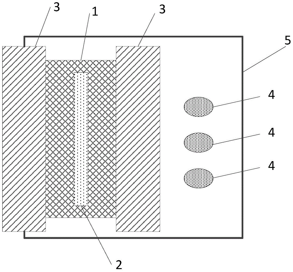
图1为本申请实施例所提供的一种新型显示装置的剖视图;1 is a cross-sectional view of a novel display device provided by an embodiment of the application;
图2为本申请实施例所提供的一种预设图案的正面示意图;2 is a schematic front view of a preset pattern provided by an embodiment of the present application;
图3为本申请实施例所提供的另一种新型显示装置的剖视图。FIG. 3 is a cross-sectional view of another novel display device provided by an embodiment of the present application.
具体实施方式Detailed ways
为了使本技术领域的人员更好地理解本申请方案,下面结合附图和具体实施方式对本申请作进一步的详细说明。显然,所描述的实施例仅仅是本申请一部分实施例,而不是全部的实施例。基于本申请中的实施例,本领域普通技术人员在没有做出创造性劳动前提下所获得的所有其他实施例,都属于本申请保护的范围。In order to make those skilled in the art better understand the solution of the present application, the present application will be further described in detail below with reference to the accompanying drawings and specific embodiments. Obviously, the described embodiments are only a part of the embodiments of the present application, but not all of the embodiments. Based on the embodiments in this application, all other embodiments obtained by those of ordinary skill in the art without creative efforts shall fall within the protection scope of this application.
在下面的描述中阐述了很多具体细节以便于充分理解本发明,但是本发明还可以采用其他不同于在此描述的其它方式来实施,本领域技术人员可以在不违背本发明内涵的情况下做类似推广,因此本发明不受下面公开的具体实施例的限制。Many specific details are set forth in the following description to facilitate a full understanding of the present invention, but the present invention can also be implemented in other ways different from those described herein, and those skilled in the art can do so without departing from the connotation of the present invention. Similar promotion, therefore, the present invention is not limited by the specific embodiments disclosed below.
正如背景技术部分所述,目前的显示装置利用发出可见光的LED作为光源,照射涂覆有钛白粉的具有字符形状的材料以使具有字符形状的材料发光,进而在低可见光透射率材料表面显示出字符。由于低可见光透射率材料对可见光的透射率很低,为了使字符显示在其表面,则需要增大光源的功率,导致能耗增加,同时,由于可见光在低可见光透射率材料内传播深度大,导致在颜色上也会发生色偏。As described in the background art section, current display devices use LEDs that emit visible light as light sources to irradiate titanium dioxide-coated material with character shapes to make the material with character shapes emit light, and then display on the surface of the material with low visible light transmittance character. Since the low visible light transmittance material has a very low transmittance to visible light, in order to display the characters on its surface, the power of the light source needs to be increased, resulting in an increase in energy consumption. Causes a color cast to occur as well.
有鉴于此,本申请提供了一种新型显示装置,请参考图1和图2,图1为本申请实施例所提供的一种新型显示装置的剖视图,图2为本申请实施例所提供的一种预设图案的正面示意图,该装置包括:In view of this, the present application provides a novel display device, please refer to FIG. 1 and FIG. 2 , FIG. 1 is a cross-sectional view of a novel display device provided by an embodiment of the present application, and FIG. 2 is an embodiment of the present application. A schematic front view of a preset pattern, the device includes:
导光介质层1,所述导光介质层1中内嵌有具有预设图案的上转换发光材料层2;a light-guiding
位于所述导光介质层1两侧的界面材料层3;
位于所述导光介质层1一侧的红外光源4,且所述红外光源4与所述导光介质层1被所述界面材料层3隔开。The
需要说明的是,在实际生产使用时还可以设置外壳5,由于容纳导光介质层1、红外光源4、界面材料层3。It should be noted that, in actual production and use, the
上转换发光材料层2内嵌在导光介质层1中是指,导光介质层1是具有一定厚度的,导光介质层1的内部具有一定的空腔,上转换发光材料层2位于空腔中。The up-conversion
所述上转换发光材料层2可以为掺有稀土元素的氟化钇钠(NaYF4)层,其中,稀土元素可以为镱和铒。本申请中对上转换发光材料层2并不做具体限定,在其他实施例中,上转换发光材料层2还可以为掺有稀土元素的氟化钙(CaF2)层,或者氧化钆(Gd2O3)层等等,由于不同的上转换发光材料具有不同的发射光谱,具体可以根据所需的发光颜色选择上转换发光材料层2。The up-conversion
可选的,所述预设图案为数字或者字母,当然还可以为其他任何形状。Optionally, the preset pattern is a number or a letter, and of course, it can be any other shape.
需要指出的是,本申请中的导光介质层1材料包括但不限于聚苯乙烯、聚碳酸酯、聚甲基丙烯酸甲酯中的任一种。It should be noted that the material of the light
还需要指出的是,本申请中对界面材料层3不做具体限定,视情况而定。例如,所述界面材料层3为皮革层,或者织物层,或者镜面,或者不透光的塑料制品层等任何低可见光透射率的材料层。It should also be pointed out that the
可选的,所述红外光源4为红外LED(Light Emitting Diode,发光二极管)或者红外激光器或者红外有机发光光源。其中,红外有机发光光源是指利用光源或者电激发红外有机发光材料而产生红外光线的光源,例如,红外有机发光材料为双核环金属铱/铂配合物的电致发光器件。Optionally, the
本申请中的新型显示装置中的光源为红外光源4,红外光源4产生红外光线,红外光线在界面材料层3中的穿透率很高,照射在上转换发光材料层2上,并且上转换发光材料层2受到能量较低的光的激发就可以发射出高能量的光,上转换发光材料层2的预设图案就可以显示在远离红外光源4的界面材料层3上,所以红外光源4所需的功率较小,降低显示预设图案的能耗,又由于在界面材料层3中传递的光线是红外光光线,传播深度小,避免发生色偏。The light source in the novel display device in the present application is an
请参考图3,图3为本申请实施例所提供的另一种新型显示装置的剖视图。在上述实施例的基础上,新型显示装置还包括:Please refer to FIG. 3 , which is a cross-sectional view of another novel display device according to an embodiment of the present application. On the basis of the above embodiments, the novel display device further includes:
位于所述界面材料层3显示所述预设图案的表面的红外线屏蔽层6,以防止新型显示装置内部红外线泄露对人眼造成伤害,同时也可以避免外部太阳光的红外分量进入新型显示装置,造成预期之外的杂散光。The
需要说明的是,本申请中对红外线屏蔽层6的材料不做具体限定,只要能够起到屏蔽红外线的作用即可。例如,红外线屏蔽层6包括氧化铟锡层以及包覆在氧化铟锡层上表面的涂层,上表面的涂层可以为二氧化硅涂层、环氧类树脂层或者丙烯酸类树脂层;进一步的,红外线屏蔽层6还可以为包括氧化铟锡层、包覆在氧化铟锡层上表面的涂层、包覆在氧化铟锡层下表面的涂层,下表面的涂层可以为氨基甲酸酯树脂层。It should be noted that the material of the
在本申请的一个实施例中,当所述新型显示装置为旋钮时,所述新型显示装置的外壳5设置有防滑纹路,以便于用户进行操作。In an embodiment of the present application, when the novel display device is a knob, the
本申请还提供一种汽车部件,所述汽车部件包括上述实施例所述的新型显示装置。The present application also provides an automobile component, which includes the novel display device described in the above embodiments.
本实施例中的汽车部件中设置有新型显示装置,新型显示装置中的光源为红外光源,红外光源产生红外光线,红外光线在界面材料层中的穿透率很高,照射在上转换发光材料层上,并且上转换发光材料层受到能量较低的光的激发就可以发射出高能量的光,上转换发光材料层的预设图案就可以显示在远离红外光源的界面材料层上,所以红外光源所需的功率较小,降低显示预设图案的能耗,又由于在界面材料层中传递的光线是红外光光线,传播深度小,避免发生色偏,从而降低汽车部件的能耗,增强实用性。In this embodiment, a new type of display device is installed in the automobile part. The light source in the new type of display device is an infrared light source, and the infrared light source generates infrared light. and the up-conversion luminescent material layer can emit high-energy light when excited by light with lower energy, and the preset pattern of the up-conversion luminescent material layer can be displayed on the interface material layer far away from the infrared light source, so the infrared The power required by the light source is small, which reduces the energy consumption of displaying the preset pattern, and because the light transmitted in the interface material layer is infrared light, the propagation depth is small, and color shift is avoided, thereby reducing the energy consumption of automobile parts and enhancing the practicality.
本说明书中各个实施例采用递进的方式描述,每个实施例重点说明的都是与其它实施例的不同之处,各个实施例之间相同或相似部分互相参见即可。对于实施例公开的装置而言,由于其与实施例公开的方法相对应,所以描述的比较简单,相关之处参见方法部分说明即可。The various embodiments in this specification are described in a progressive manner, and each embodiment focuses on the differences from other embodiments, and the same or similar parts between the various embodiments may be referred to each other. As for the device disclosed in the embodiment, since it corresponds to the method disclosed in the embodiment, the description is relatively simple, and the relevant part can be referred to the description of the method.
以上对本申请所提供的新型显示装置和汽车部件进行了详细介绍。本文中应用了具体个例对本申请的原理及实施方式进行了阐述,以上实施例的说明只是用于帮助理解本申请的方法及其核心思想。应当指出,对于本技术领域的普通技术人员来说,在不脱离本申请原理的前提下,还可以对本申请进行若干改进和修饰,这些改进和修饰也落入本申请权利要求的保护范围内。The novel display device and automobile parts provided by the present application have been introduced in detail above. Specific examples are used herein to illustrate the principles and implementations of the present application, and the descriptions of the above embodiments are only used to help understand the methods and core ideas of the present application. It should be pointed out that for those of ordinary skill in the art, without departing from the principles of the present application, several improvements and modifications can also be made to the present application, and these improvements and modifications also fall within the protection scope of the claims of the present application.
Claims (9)
Priority Applications (1)
| Application Number | Priority Date | Filing Date | Title |
|---|---|---|---|
| CN202010928716.3A CN111880259B (en) | 2020-09-07 | 2020-09-07 | Novel display device and automobile part |
Applications Claiming Priority (1)
| Application Number | Priority Date | Filing Date | Title |
|---|---|---|---|
| CN202010928716.3A CN111880259B (en) | 2020-09-07 | 2020-09-07 | Novel display device and automobile part |
Publications (2)
| Publication Number | Publication Date |
|---|---|
| CN111880259A CN111880259A (en) | 2020-11-03 |
| CN111880259B true CN111880259B (en) | 2022-10-18 |
Family
ID=73198914
Family Applications (1)
| Application Number | Title | Priority Date | Filing Date |
|---|---|---|---|
| CN202010928716.3A Active CN111880259B (en) | 2020-09-07 | 2020-09-07 | Novel display device and automobile part |
Country Status (1)
| Country | Link |
|---|---|
| CN (1) | CN111880259B (en) |
Families Citing this family (1)
| Publication number | Priority date | Publication date | Assignee | Title |
|---|---|---|---|---|
| WO2024004867A1 (en) * | 2022-06-30 | 2024-01-04 | Dic株式会社 | Display apparatus and display method |
Family Cites Families (9)
| Publication number | Priority date | Publication date | Assignee | Title |
|---|---|---|---|---|
| US7466896B2 (en) * | 2005-10-26 | 2008-12-16 | The Hong Kong Polytechnic University | Photonic fabric display with controlled pattern, color, luminescence intensity, scattering intensity and light self-amplification |
| US10125931B2 (en) * | 2008-03-01 | 2018-11-13 | Goldeneye, Inc. | Barrier with integrated self cooling solid state light sources |
| CN102269907A (en) * | 2010-06-04 | 2011-12-07 | 电子科技大学 | Wavelength converter for infrared light and visible light |
| US20140097356A1 (en) * | 2012-10-04 | 2014-04-10 | Electronics And Telecommunications Research Institute | Display device |
| KR20160030225A (en) * | 2013-07-10 | 2016-03-16 | 골든아이 인코퍼레이티드 | Self cooling light source |
| KR102448375B1 (en) * | 2015-12-18 | 2022-09-29 | 경기대학교 산학협력단 | invisible display device |
| JP2017161755A (en) * | 2016-03-10 | 2017-09-14 | パナソニックIpマネジメント株式会社 | Light-emitting device and illumination apparatus including the same |
| KR102460111B1 (en) * | 2017-09-07 | 2022-10-28 | 엘지디스플레이 주식회사 | Flat Panel Display Embedding Optical Imaging Sensor |
| CN110634692A (en) * | 2019-10-30 | 2019-12-31 | 科世达(上海)机电有限公司 | A new type switchable character display switch and device |
-
2020
- 2020-09-07 CN CN202010928716.3A patent/CN111880259B/en active Active
Also Published As
| Publication number | Publication date |
|---|---|
| CN111880259A (en) | 2020-11-03 |
Similar Documents
| Publication | Publication Date | Title |
|---|---|---|
| US10624173B2 (en) | Invisible, light-transmissive display system | |
| WO2007103394A3 (en) | Light emitting sign and display surface therefor | |
| US20120055055A1 (en) | Systems and Method for Outdoor Media Signage | |
| TW200500594A (en) | OLED display with photosensor | |
| CN102831837B (en) | Transparent display panel and display device | |
| JP2011095699A (en) | Window, method of manufacturing the same, and electronic device employing the same | |
| CN111880259B (en) | Novel display device and automobile part | |
| JPWO2011152446A1 (en) | Light guide plate and lighting device | |
| KR20120119748A (en) | Wood sign having illuminating portion and manufacturing method of the same | |
| US6591530B1 (en) | Dynamic picture set | |
| CN2938613Y (en) | Light plate keyboard of mobile terminal | |
| JP2019066657A (en) | Display device, display system, and electrical equipment | |
| JP2006053449A (en) | Surface light emitting device | |
| JPH06186525A (en) | Plate material for decoration | |
| CN201616246U (en) | Optical display device | |
| CN103443671B (en) | There is the mosaic luminaire of transparent body with the multiple photoconductions demarcated by slit | |
| JP2009258459A (en) | Light-emitting display device | |
| KR200264961Y1 (en) | Illumination Signboard Using Fluorescent Resin | |
| JPH06274113A (en) | Display device | |
| KR20140044142A (en) | Display device | |
| CN221991592U (en) | A touch display with full-body luminescence | |
| KR20140044140A (en) | Display device | |
| CN213509099U (en) | Jade light-passing board | |
| CN110634692A (en) | A new type switchable character display switch and device | |
| CN216647780U (en) | Luminous sign and electronic equipment |
Legal Events
| Date | Code | Title | Description |
|---|---|---|---|
| PB01 | Publication | ||
| PB01 | Publication | ||
| SE01 | Entry into force of request for substantive examination | ||
| SE01 | Entry into force of request for substantive examination | ||
| GR01 | Patent grant | ||
| GR01 | Patent grant |