CN111799241A - Bonding structure, method of making the same, and display panel - Google Patents
Bonding structure, method of making the same, and display panel Download PDFInfo
- Publication number
- CN111799241A CN111799241A CN202010585900.2A CN202010585900A CN111799241A CN 111799241 A CN111799241 A CN 111799241A CN 202010585900 A CN202010585900 A CN 202010585900A CN 111799241 A CN111799241 A CN 111799241A
- Authority
- CN
- China
- Prior art keywords
- electrode
- conductive
- bonding structure
- array
- conductive pillars
- Prior art date
- Legal status (The legal status is an assumption and is not a legal conclusion. Google has not performed a legal analysis and makes no representation as to the accuracy of the status listed.)
- Pending
Links
Images


Classifications
-
- H—ELECTRICITY
- H10—SEMICONDUCTOR DEVICES; ELECTRIC SOLID-STATE DEVICES NOT OTHERWISE PROVIDED FOR
- H10K—ORGANIC ELECTRIC SOLID-STATE DEVICES
- H10K59/00—Integrated devices, or assemblies of multiple devices, comprising at least one organic light-emitting element covered by group H10K50/00
- H10K59/10—OLED displays
- H10K59/12—Active-matrix OLED [AMOLED] displays
- H10K59/123—Connection of the pixel electrodes to the thin film transistors [TFT]
-
- H10W72/01212—
-
- H10W72/07231—
-
- H10W72/234—
-
- H10W72/242—
Landscapes
- Engineering & Computer Science (AREA)
- Microelectronics & Electronic Packaging (AREA)
- Combinations Of Printed Boards (AREA)
Abstract
本申请涉及一种邦定结构、其制作方法和显示面板。所述邦定结构包括第一器件、第二器件和导电柱阵列。所述第一器件包括第一电极。所述第二器件与所述第一器件相对设置。所述第二器件包括第二电极。所述导电柱阵列夹设于所述第一电极和所述第二电极之间,将所述第一电极和所述第二电极电连接。所述导电柱阵列的两端可以分别与所述第一电极和所述第二电极接触连接,因此通过设定所述导电柱阵列的两端与所述第一电极和所述第二电极之间的接触面积,可以确保所述第一电极和所述第二电极之间具有良好的电接触。通过使所述导电柱阵列的两端分别所述第一电极和第二电极接触,即可达到电路导通的目的。
The present application relates to a bonding structure, a manufacturing method thereof and a display panel. The bonding structure includes a first device, a second device, and an array of conductive pillars. The first device includes a first electrode. The second device is disposed opposite to the first device. The second device includes a second electrode. The conductive column array is sandwiched between the first electrode and the second electrode, and electrically connects the first electrode and the second electrode. Both ends of the conductive column array can be in contact with the first electrode and the second electrode respectively. Therefore, by setting the distance between the two ends of the conductive column array and the first electrode and the second electrode, the The contact area between the two electrodes can ensure good electrical contact between the first electrode and the second electrode. By making the two ends of the conductive column array respectively contact the first electrode and the second electrode, the purpose of circuit conduction can be achieved.
Description
技术领域technical field
本发明涉及显示技术领域,特别是涉及邦定结构及其制作方法和显示面板。The present invention relates to the field of display technology, in particular to a bonding structure and a manufacturing method thereof and a display panel.
背景技术Background technique
随着显示技术的发展,对面板与元器件之间的电连接要求越来越高。With the development of display technology, the requirements for the electrical connection between the panel and the components are getting higher and higher.
传统技术中,面板的焊盘和元器件的焊盘之间电连接是通过异方性导电胶(ACF)中粒子被压破后里面露出的金属粒子实现的。但是异方性导电胶对焊盘和焊盘之间的接触面积要求较高,当接触面积较小时,在焊盘和焊盘之间的金属粒子数量较少,影响导电效果。In the traditional technology, the electrical connection between the pads of the panel and the pads of the components is realized by the metal particles exposed inside the anisotropic conductive adhesive (ACF) after the particles are crushed. However, the anisotropic conductive adhesive has higher requirements on the contact area between the pad and the pad. When the contact area is small, the number of metal particles between the pad and the pad is small, which affects the conductive effect.
发明内容SUMMARY OF THE INVENTION
基于此,有必要针对上述问题,提供一种邦定结构及其制作方法和显示面板。Based on this, it is necessary to provide a bonding structure and a manufacturing method thereof and a display panel for the above problems.
本申请一方面提供了一种邦定结构,包括:第一器件,包括第一电极;第二器件,与所述第一器件相对设置,所述第二器件包括第二电极;以及导电柱阵列,夹设于所述第一电极和所述第二电极之间,用于将所述第一电极和所述第二电极电连接。In one aspect of the present application, a bonding structure is provided, including: a first device including a first electrode; a second device disposed opposite to the first device, the second device including a second electrode; and a conductive column array , which is sandwiched between the first electrode and the second electrode and used to electrically connect the first electrode and the second electrode.
在一个实施例中,所述导电柱阵列包括并列设置的多个导电柱,所述多个导电柱由所述第一电极向所述第二电极的方向延伸。本实施例提供了导电柱延伸方向的可实施方式。In one embodiment, the conductive column array includes a plurality of conductive columns arranged in parallel, the plurality of conductive columns extending from the first electrode to the direction of the second electrode. This embodiment provides possible implementations of the extending direction of the conductive pillars.
在一个实施例中,所述多个导电柱间隔设置。本实施例中,所述导电柱和所述导电柱之间可以具有空隙。所述空隙可以填充胶体,进而增加胶体和所述导电柱侧壁之间的接触面积。In one embodiment, the plurality of conductive pillars are arranged at intervals. In this embodiment, there may be gaps between the conductive pillars and the conductive pillars. The voids can be filled with colloid, thereby increasing the contact area between the colloid and the sidewalls of the conductive pillars.
在一个实施例中,沿平行于所述第一电极的方向,所述多个导电柱的横截面积由所述第一电极向所述第二电极的方向梯度变小;优选地,所述导电柱的形状为锥体。本实施例可以便于所述导电柱插入所述胶体中。In one embodiment, along a direction parallel to the first electrode, the cross-sectional area of the plurality of conductive pillars becomes smaller in a gradient direction from the first electrode to the second electrode; preferably, the The shape of the conductive column is a cone. This embodiment can facilitate the insertion of the conductive post into the colloid.
在一个实施例中,所述导电柱包括多个圆台,多个所述圆台的底部和顶部依次连接。导电柱还可以包括圆台结构,提供了导电柱的一种可实施方式。In one embodiment, the conductive column includes a plurality of circular truncated cones, and the bottoms and the tops of the plurality of circular truncated truncated cones are connected in sequence. The conductive pillars may also include truncated truncated structures, providing one possible embodiment of the conductive pillars.
在一个实施例中,所述导电柱阵列还包括多个导电颗粒,每个所述导电柱远离所述第一电极的一端通过一个所述导电颗粒与所述第二电极接触。本实施例中,所述导电颗粒与第二电极的凹坑内表面贴合的面积较大,因此可以增加导电面积,降低导通电阻。In one embodiment, the conductive pillar array further includes a plurality of conductive particles, and one end of each of the conductive pillars away from the first electrode is in contact with the second electrode through one of the conductive particles. In this embodiment, the area where the conductive particles are attached to the inner surface of the pit of the second electrode is relatively large, so the conductive area can be increased and the on-resistance can be reduced.
在一个实施例中,还包括胶体层,夹设于所述第一器件和所述第二器件之间,所述导电柱阵列位于所述胶体层中。本实施例通过所述胶体层可以增加所述第一电极和所述第二电极连接的牢固性。In one embodiment, a colloidal layer is further included, sandwiched between the first device and the second device, and the conductive column array is located in the colloidal layer. In this embodiment, the colloid layer can increase the firmness of the connection between the first electrode and the second electrode.
本申请另一方面提供了一种邦定结构的制作方法,包括:提供第一器件,所述第一器件包括第一电极;在所述第一电极的表面形成导电柱阵列;将第二器件与所述第一器件相对靠近,使得所述第二器件的第二电极接触所述导电柱阵列远离所述第一器件的表面。Another aspect of the present application provides a method for fabricating a bonding structure, including: providing a first device, the first device including a first electrode; forming a conductive column array on the surface of the first electrode; Relatively close to the first device such that the second electrode of the second device contacts a surface of the array of conductive pillars remote from the first device.
在一个实施例中,所述在所述第一电极的表面形成导电柱阵列的步骤中,所述导电柱阵列与所述第一电极一体成型。本实施例可以提高所述导电柱阵列与所述第一电极连接的牢固性,同时还简化了工艺步骤。In one embodiment, in the step of forming a conductive column array on the surface of the first electrode, the conductive column array is integrally formed with the first electrode. This embodiment can improve the firmness of the connection between the conductive column array and the first electrode, and also simplifies the process steps.
本申请还一方面提供了一种显示面板,其特征在于,包括所述的邦定结构或由所述的邦定结构的制作方法制作得到的邦定结构;其中,所述第一器件为面板主体,所述第二器件为元器件。Another aspect of the present application provides a display panel, which is characterized in that it includes the bonding structure or the bonding structure produced by the manufacturing method of the bonding structure; wherein, the first device is a panel The main body, the second device is a component.
本申请实施例提供的邦定结构及其制作方法和显示面板,该邦定结构包括第一器件、第二器件和导电柱阵列。其中,第一器件包括第一电极;第二器件与第一器件相对设置,第二器件包括第二电极;导电柱阵列夹设于第一电极和第二电极之间,用于将第一电极和第二电极电连接。由于导电柱阵列的两端可以分别与第一电极和第二电极接触连接,因此通过设定导电柱阵列的两端与第一电极和第二电极之间的接触面积,可以确保第一电极和第二电极之间具有良好的电接触,即可达到电路导通的目的。同时可以避免高温、高压挤压第一电极和第二电极而导致得第一器件或者第二器件发生损坏的问题。The bonding structure and the manufacturing method thereof, and the display panel provided by the embodiments of the present application, the bonding structure includes a first device, a second device and a conductive column array. Wherein, the first device includes a first electrode; the second device is disposed opposite to the first device, the second device includes a second electrode; the conductive column array is sandwiched between the first electrode and the second electrode for connecting the first electrode is electrically connected to the second electrode. Since both ends of the conductive column array can be in contact with the first electrode and the second electrode, respectively, by setting the contact area between the two ends of the conductive column array and the first electrode and the second electrode, the first electrode and the second electrode can be ensured. With good electrical contact between the second electrodes, the purpose of circuit conduction can be achieved. At the same time, the problem of damage to the first device or the second device caused by pressing the first electrode and the second electrode at high temperature and high pressure can be avoided.
附图说明Description of drawings
为了更清楚地说明本申请实施例或现有技术中的技术方案,下面将对实施例或现有技术描述中所需要使用的附图作简单地介绍,显而易见地,下面描述中的附图仅仅是本申请的一些实施例,对于本领域普通技术人员来讲,在不付出创造性劳动的前提下,还可以根据这些附图获得其他的附图。In order to more clearly illustrate the embodiments of the present application or the technical solutions in the prior art, the following briefly introduces the accompanying drawings required for the description of the embodiments or the prior art. Obviously, the drawings in the following description are only These are some embodiments of the present application. For those of ordinary skill in the art, other drawings can also be obtained based on these drawings without any creative effort.
图1为本申请实施例提供的邦定结构剖面图;1 is a cross-sectional view of a bonding structure provided in an embodiment of the present application;
图2为本申请另一个实施例提供的邦定结构剖面图;2 is a cross-sectional view of a bonding structure provided by another embodiment of the present application;
图3为本申请实施例提供的导电柱包括圆台的剖面图;3 is a cross-sectional view of a conductive column including a truncated cone provided by an embodiment of the present application;
图4为本申请还一个实施例提供的邦定结构剖面图;4 is a cross-sectional view of a bonding structure provided by yet another embodiment of the present application;
图5为本申请实施例提供的导电柱通过导电颗粒与第二电极连接的剖面图。FIG. 5 is a cross-sectional view of a conductive pillar connected to a second electrode through conductive particles according to an embodiment of the present application.
附图标记说明:Description of reference numbers:
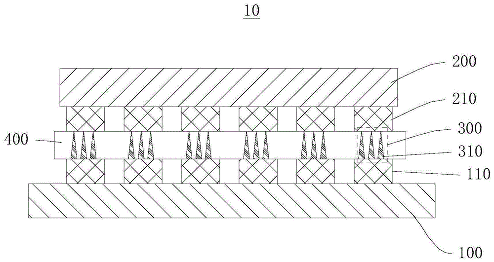
邦定结构10;第一器件100;第一电极110;第二器件200;第二电极210;导电柱阵列300;导电柱310;圆台312;导电颗粒320;胶体层400。
具体实施方式Detailed ways
为使本发明的上述目的、特征和优点能够更加明显易懂,下面结合附图对本发明的具体实施方式做详细的说明。在下面的描述中阐述了很多具体细节以便于充分理解本发明。但是本发明能够以很多不同于在此描述的其它方式来实施,本领域技术人员可以在不违背本发明内涵的情况下做类似改进,因此本发明不受下面公开的具体实施例的限制。In order to make the above objects, features and advantages of the present invention more clearly understood, the specific embodiments of the present invention will be described in detail below with reference to the accompanying drawings. In the following description, numerous specific details are set forth in order to provide a thorough understanding of the present invention. However, the present invention can be implemented in many other ways different from those described herein, and those skilled in the art can make similar improvements without departing from the connotation of the present invention. Therefore, the present invention is not limited by the specific embodiments disclosed below.
在本发明的描述中,需要理解的是,术语“中心”、“纵向”、“横向”、“长度”、“宽度”、“厚度”、“上”、“下”、“前”、“后”、“左”、“右”、“竖直”、“水平”、“顶”、“底”、“内”、“外”、“顺时针”、“逆时针”、“轴向”、“径向”、“周向”等指示的方位或位置关系为基于附图所示的方位或位置关系,仅是为了便于描述本发明和简化描述,而不是指示或暗示所指的装置或元件必须具有特定的方位、以特定的方位构造和操作,因此不能理解为对本发明的限制。需要说明的是,当元件被称为“固定于”或“设置于”另一个元件,它可以直接在另一个元件上或者也可以存在居中的元件。In the description of the present invention, it should be understood that the terms "center", "longitudinal", "lateral", "length", "width", "thickness", "upper", "lower", "front", " Back, Left, Right, Vertical, Horizontal, Top, Bottom, Inner, Outer, Clockwise, Counterclockwise, Axial , "radial", "circumferential" and other indicated orientations or positional relationships are based on the orientations or positional relationships shown in the accompanying drawings, and are only for the convenience of describing the present invention and simplifying the description, rather than indicating or implying the indicated device or Elements must have a particular orientation, be constructed and operate in a particular orientation and are therefore not to be construed as limitations of the invention. It should be noted that when an element is referred to as being "fixed to" or "disposed on" another element, it can be directly on the other element or an intervening element may also be present.
此外,术语“第一”、“第二”仅用于描述目的,而不能理解为指示或暗示相对重要性或者隐含指明所指示的技术特征的数量。由此,限定有“第一”、“第二”的特征可以明示或者隐含地包括至少一个该特征。在本发明的描述中,“多个”的含义是至少两个,例如两个,三个等,除非另有明确具体的限定。In addition, the terms "first" and "second" are only used for descriptive purposes, and should not be construed as indicating or implying relative importance or implying the number of indicated technical features. Thus, a feature delimited with "first", "second" may expressly or implicitly include at least one of that feature. In the description of the present invention, "plurality" means at least two, such as two, three, etc., unless otherwise expressly and specifically defined.
申请人长期研究发现,器件之间的焊盘和引脚通常通过异方性导电胶连接。当需要电连接所述焊盘和所述引脚时,通常在所述焊盘和所述引脚之间涂覆所述异方性导电胶。然后通过压头在高温下压迫器件,使得所述焊盘和所述引脚相互靠近。同时,所述异方性导电胶中的粒子被压破,使得其中的导电粒子露出。分散在所述异方性导电胶中的导电粒子相互靠近接触,并与所述焊盘和引脚相互接触导电。但是,当所述焊盘或者所述引脚相对的面积较小时,或者所述焊盘和所述引脚对接产生错位时,或者由于所述导电粒子密度分布不均匀时,能够连接所述引脚或者焊盘的所述导电粒子数量较少,从而影响导电的效果。如果所述焊盘和所述引脚错位严重时,可能引起短路。The applicant's long-term research found that the pads and pins between the devices are usually connected by anisotropic conductive glue. When the pads and the pins need to be electrically connected, the anisotropic conductive glue is usually coated between the pads and the pins. The device is then pressed at a high temperature by an indenter, so that the pads and the pins are brought close to each other. At the same time, the particles in the anisotropic conductive adhesive are crushed, so that the conductive particles therein are exposed. The conductive particles dispersed in the anisotropic conductive adhesive are in close contact with each other, and are in contact with the pads and pins to conduct electricity. However, when the relative area of the pads or the pins is small, or when the bonding pads and the pins are misaligned, or due to uneven density distribution of the conductive particles, the pins can be connected to each other. The number of the conductive particles of the feet or pads is small, thereby affecting the effect of conduction. If the pad and the pin are seriously misaligned, a short circuit may be caused.
参阅图1,本申请实施例提供一种邦定结构10。所述邦定结构10包括第一器件100、第二器件200和导电柱阵列300。所述第一器件100包括第一电极110。所述第二器件200与所述第一器件100相对设置,所述第二器件200包括第二电极210。所述导电柱阵列300夹设于所述第一电极110和所述第二电极210之间,所述导电柱阵列300用于将所述第一电极110和所述第二电极210电连接。Referring to FIG. 1 , an embodiment of the present application provides a
在一个实施例中,所述第一器件100可以为柔性线路板、驱动芯片、触摸屏驱动芯片等。所述第二器件200可以为显示面板主体。可以理解,所述第一器件100也可以为显示面板主体,所述第二器件200可以为柔性线路板、驱动芯片、触摸屏驱动芯片,具体可根据实际情况进行设置。In one embodiment, the
所述第一电极110和所述第二电极210可以为形成于所述第一器件100和所述第二器件200的焊盘、引脚等结构。所述第一器件100和所述第二器件200需要电连接时,可以将所述第一电极110和所述第二电极210对应连接。可以理解,每个所述第一器件100可以包括多个第一电极110。每个所述第二器件200可以包括多个第二电极210。多个所述第一电极110和多个所述第二电极210可以一一对应设置。即一一对应的所述第一电极110和所述第二电极210可以形成一个导电通路。The
在一个实施例中,所述第一电极110和所述第二电极210至少一个可以为多层金属结构。所述第一电极和所述第二电极的材料可以包括钼、镍、钯、钴、钨、铑、钛、铬、金、银、铂等。In one embodiment, at least one of the
在一个实施例中,所述第一电极110和/或所述第二电极210可以为层叠设置的至少两层金属层。例如,第一电极110和/或所述第二电极210可以为层叠设置的第一金属层、第二金属层和第三金属层结构。所述第一金属层与所述第三金属层的金属材料可采用钼、镍、钯、钴、钨、铑、钛、铬、金、银、铂等耐腐蚀性好的材料。所述第二金属层可以采用用金、银、铜、铝、铁等导电性良好的材料。In one embodiment, the
在一个实施例中,所述第一电极110和所述第二电极210可以为立方体结构,该立方体结构在所述第一器件100或第二器件200的表面的投影为矩形。所述矩形的宽度可以为10微米到200微米。所述矩形的长度为80微米到2毫米。进一步地,所述第一电极110和/或所述第二电极210的宽度可以为20微米,长度为100微米。In one embodiment, the
所述导电柱阵列300可以包括多个导电柱310。每对一一对应的所述第一电极110和所述第二电极210之间可以设置一个所述导电柱阵列300。所述导电柱阵列300设置于所述第一电极110和所述第二电极210之间。所述多个导电柱310在所述第一电极110和所述第二电极210相对的表面排列,构成所述导电柱阵列300。所述导电柱阵列300可以为矩形阵列、圆形阵列或者线性阵列等。所述导电柱阵列300的两端可以分别与所述第一电极110和所述第二电极210相对的两个表面接触。因此,所述导电柱阵列300可以将所述第一电极110和所述第二电极210电连接。The
在一个实施例中,所述导电柱阵列300可以为矩形阵列,所述矩形阵列在所述第一器件100或所述第二器件200的投影可以为矩形。所述矩形的宽度可以为8微米到70微米,所述导电柱阵列300的长度可以为15微米到180微米。In one embodiment, the
所述导电柱阵列300的两端可以分别与所述第一电极110和所述第二电极210连接。因此,可以通过设定所述导电柱阵列300的两端与所述第一电极110和所述第二电极210的接触面积,保证所述导电柱阵列300与所述第一电极110和所述第二电极210之间接触面积,从而确保了所述第一电极110和所述第二电极210之间导电效果。同时,由于所述导电柱阵列300形状相对固定,相比所述第一电极110和所述第二电极210接触时异方性导电胶中的导电粒子分布的随机性,更具有稳定性。进一步地,使用所述导电柱阵列300连接所述第一电极110和所述第二电极210,只要所述导电柱阵列300的两端分别与所述第一电极110和第二电极210接触即可。因此可以避免使用异方性导电胶时需要高温、高压将所述第一电极110和第二电极210连接,从而导致所述第一器件100或者所述第二器件200发生损坏的问题。Two ends of the
本申请实施例提供的所述邦定结构10包括第一器件100、第二器件200和导电柱阵列300。所述第一器件100包括第一电极110。所述第二器件200与所述第一器件100相对设置。所述第二器件200包括第二电极210。所述导电柱阵列300夹设于所述第一电极110和所述第二电极210之间。所述导电柱阵列300用于将所述第一电极110和所述第二电极210电连接。所述导电柱阵列300的两端可以分别与所述第一电极110和所述第二电极210接触连接,因此通过设定所述导电柱阵列300的两端与所述第一电极110和所述第二电极210之间的接触面积,可以确保所述第一电极110和所述第二电极210之间具有良好的电接触。通过使所述导电柱阵列300的两端分别与所述第一电极110和第二电极210接触,即可达到电路导通的目的。同时可以避免高温、高压挤压所述第一电极110和第二电极210导致所述第一器件100或者第二器件200损坏。The
在一个实施例中,所述导电柱阵列300包括多个所述导电柱310,这里的多个指两个及以上。所述导电柱310由所述第一电极110向所述第二电极210的方向延伸。即所述导电柱310竖直设置于所述第一电极110和所述第二电极210之间。具体的,多个所述导电柱310并列设置。所述导电柱310两端分别与所述第一电极110和所述第二电极210连接。通过设定所述导电柱310两端的横截面积,即可确定所述导电柱310与所述第一电极110和所述第二电极210的电接触面积,从而确保所述第一电极110和所述第二电极210之间的导电性能。In one embodiment, the
在一个实施例中,一个所述导电柱阵列300可以包括2到5个所述导电柱310。进一步地,一个所述导电柱阵列300可以包括3个所述导电柱310。In one embodiment, one of the
在一个实施例中,所述导电柱310的材料可以为镍、钯、钴、钨、铑、钛、铬、金、银、铂中的一种或者多种。In one embodiment, the material of the
在一个实施例中,所述导电柱310可以为由内而外的多层结构。所述导电柱310外层材料可以采用耐腐蚀性较好的钼、镍、钯、钴、钨、铑、钛、铬、金、银、铂材料,因而可以避免被胶体腐蚀。In one embodiment, the
所述导电柱310可以为圆柱形,也可以为立方体、锥体等形状。所述导电柱310由所述第一电极110向所述第二电极210延伸的距离可以为所述导电柱310的高度。通过设定所述导电柱310的高度可以限定所述第一电极110和所述第二电极210之间的距离。The
在一个实施例中,所述导电柱310的高度可以为3微米到10微米,在保证第一电极110和第二电极210导通的基础上能进一步节约材料,降低成本。进一步地,所述导电柱310的高度可以为5微米到8微米。更进一步地,所述导电柱310的高度可以为7微米。In one embodiment, the height of the
在一个实施例中,所述导电柱310的直径可以为1微米到8微米,在此数值范围内工艺上易于制作。进一步地,所述导电柱的直径可以为2微米到3微米。在一个实施例中,所述导电柱的直径为2微米。In one embodiment, the diameter of the
多个所述导电柱310并列设置即所述多个所述导电柱310可以分别为独立结构,设置于所述第一电极110和所述第二电极210之间。多个所述导电柱310也可以部分相互接触或者一体成型。A plurality of the
在一个实施例中,在所述第一电极110和所述第二电极210之间的所述导电柱阵列300周围的空间可以通过胶体填充粘接。因而可以确保所述第一电极110和所述第二电极210连接的可靠性。In one embodiment, the space around the
请参见图2,在一个实施例中,所述多个导电柱310间隔设置。因此,导电柱阵列300中的多个所述导电柱310之间可以具有空隙。通过在所述第一电极110和所述第二电极210之间填充胶体,可以增加胶体和所述导电柱310侧壁之间的接触面积,提高两者间的粘附性。同时,胶体还分别与所述第一电极110和所述第二电极210相对的表面接触。因此,可以提高所述第一电极110、所述第二电极210和所述导电柱310之间的粘附性。同时提高了所述第一电极110、所述第二电极210和所述导电柱310整体的牢固性。在一个实施例中,所述导电柱310的侧壁可以为粗糙表面,因而可以提高胶体与所述导电柱310之间的粘附力。Referring to FIG. 2 , in one embodiment, the plurality of
在一个实施例中,沿平行于第一电极110的方向,所述多个导电柱310的横截面积由所述第一电极110向所述第二电极210的方向梯度变小。即所述多个导电柱310的横截面积由所述第一电极110向所述第二电极210的方向具有变小的趋势。因此所述导电柱310远离所述第一电极110的一端横截面积比所述导电柱310靠近所述第一电极110一端的横截面积更小。In one embodiment, along a direction parallel to the
当所述导电柱310设置于所述第一电极110,在所述第一电极110的表面涂覆胶体时,由于所述导电柱310远离所述第一电极110的一端横截面积小,便于所述导电柱310插入所述胶体。可选的,胶体可以设置在第二电极210上,也可以设置在其他结构上,具体可根据实际情况进行设置。在一个实施例中,所述导电柱310的形状为锥体,制作锥体的方式工艺简单,能够降低生产成本。When the
进一步地,当向多个所述导电柱310之间填充胶体时,在沿着由所述第一电极110到所述第二电极210的延伸方向,所述胶体的含量也会变化,从而可以改变所述胶体和所述导电柱310在不同位置的接触面积,进一步提高粘附力。即当所述梯度较大时,由所述第一电极110向所述第二电极210的方向,所述导电柱310的直径变化较大。当所述梯度较小时,由所述第一电极110向所述第二电极210的方向,所述导电柱310的直径变化较小。进一步地,当所述梯度变化为零时,所述导电柱310不同位置的直径可以相同。更进一步地,在所述导电柱310的某一区域,所述导电柱310直径的梯度可以突变,即所述导电柱310的直径可以突变。可以理解的是,本实施例中的导电柱310直径为导电柱310的横截面积的外围边中两点间的最大距离。Further, when the colloid is filled between the plurality of the
请参见图3,在一个实施例中,所述导电柱310包括多个圆台312。多个所述圆台312的底部(靠近第一电极110一面)和顶部(靠近第二电极210的一面)依次连接。可以理解,所述圆台312的底部面积大于所述圆台312的顶部面积。第一个所述圆台312的顶部与另一个所述圆台312的底部相接触,照此依次连接构成所述导电柱310。因此,所述导电柱310在轴向的表面面积会有多个突变,当在所述导电柱310之间填充胶体时,可以增加胶体与所述导电柱310之间的粘附面积,增加粘附牢固性。Referring to FIG. 3 , in one embodiment, the
在一个实施例中,所述多个导电柱310与所述第一电极110一体成型。因此,所述导电柱310可以形成于所述第一电极110的表面。所述多个导电柱310远离所述第一电极110的一端与所述第二电极210接触。In one embodiment, the plurality of
在一个实施例中,所述导电柱310可以通过沉积、曝光、刻蚀工艺形成于所述第一电极110的表面。In one embodiment, the
请参见图4,在一个实施例中,所述导电柱310可以设置于所述第二电极210与所述第一电极110相对的表面。此时可以在所述第一电极110的表面涂覆胶体,然后将所述第二电极210与所述第一电极110相对贴近。此时所述导电柱310远离所述第二电极210的一端可以快速插入胶体。Referring to FIG. 4 , in one embodiment, the
请参见图5,在一个实施例中,所述导电柱阵列300还包括多个导电颗粒320。每个所述导电柱310远离所述第一电极110的一端通过一个所述导电颗粒320与所述第二电极210接触。可以理解,所述第二电极210的表面一般为粗糙面,即所述第二电极210的表面会有凹坑结构。因此,当所述导电柱310远离所述第一电极110的一端通过所述导电颗粒320与所述第二电极210的粗糙面抵接时,所述导电颗粒320可以嵌入所述凹坑结构。因此可以增加所述导电柱310与所述第二电极210之间的牢固性。进一步地,所述导电颗粒320与所述凹坑内表面贴合的面积较大,因此可以增加导电面积,降低导通电阻。Referring to FIG. 5 , in one embodiment, the
在一个实施例中,所述导电颗粒320的材料可以是导电性良好的金、银、铂材料中的一种或者多种,因此可以改善导电性能。所述导电颗粒320的形状可以为球形、不规则多边形等。In one embodiment, the material of the
在一个实施例中,所述导电颗粒320可以与所述导电柱310一体成型,也可以粘贴于所述导电柱310远离所述第一电极110的一端。可以理解,为了适应所述导电颗粒320的尺寸,也可以在所述第二电极210的表面制作与所述导电颗粒320尺寸相适应的凹坑结构。In one embodiment, the
在一个实施例中,所述导电颗粒320的直径可以为0.5微米到1微米。进一步地,所述导电颗粒320的直径为0.7微米,该尺寸可以适应所述第二电极210的粗糙面的凹坑结构。In one embodiment, the diameter of the
在一个实施例中,所述邦定结构10还包括胶体层400。所述胶体层400夹设于所述第一器件100和所述第二器件200之间。所述导电柱阵列300位于所述胶体层400中。所述胶体层400可以包括胶体。当所述导电柱阵列300设置于所述第一电极110时,可以在所述导电柱阵列300表面覆涂所述胶体层400,并使所述导电柱阵列300插入所述胶体层400。或者,可以在所述第二电极210表面涂覆所述胶体层400,然后将所述第一电极110设置所述导电柱阵列300的表面靠近所述胶体层400,使得所述导电柱阵列300插入所述胶体层400。通过所述胶体层400可以增加所述第一电极110和所述第二电极210连接的牢固性。所述胶体层400的材料可以为树脂凝胶。所述树脂凝胶可以包括热塑性树脂或热固性树脂等。所述胶体层400的材料也可以为丙烯酸酯胶、复合型结构胶、高分子胶、热熔胶、压敏胶等。In one embodiment, the
本申请实施例还提供一种邦定结构10的制作方法。所述方法包括:The embodiment of the present application also provides a method for fabricating the
S10,提供第一器件100,所述第一器件100包括所述第一电极110;S10, a
S20,在所述第一电极110的表面形成导电柱阵列300;S20, forming a
S30,将第二器件200与所述第一器件100相对靠近,使得所述第二器件的第二电极210接触所述导电柱阵列300远离所述第一器件100的表面。S30, the
具体的,在S10中,所述第一器件100可以为显示面板主体。所述显示面板主体的表面可以具有第一电极110。所述第一电极110可以为焊盘。Specifically, in S10, the
所述S20中,可以通过沉积、曝光、刻蚀等工序在所述第一电极110的表面形成所述导电柱阵列300。In the S20, the
所述S30中,所述第二器件200的表面设置的所述第二电极210可以为引脚。将第二器件200设置所述第二电极210的表面靠近所述第一器件100设置所述导电柱阵列300的表面,使得所述第二电极210接触所述导电柱阵列300远离所述第一器件100的表面,因此所述导电柱310可以将所述第一电极110和所述第二电极210电连接。In the S30, the
在一个实施例中,在所述第二电极210接触所述导电柱阵列300远离所述第一器件100的表面之前,可以在所述第一电极110的表面涂覆胶体层400。当所述导电柱阵列300插入所述胶体层400,然后将所述第二电极210覆盖于所述导电柱阵列300远离所述第一电极110的表面。In one embodiment, before the
在一个实施例中,所述在所述第一电极110的表面形成导电柱阵列300中,所述导电柱阵列300与所述第一电极110一体成型。所述导电柱阵列300与所述第一电极110一体成型可以提高所述导电柱阵列300与所述第一电极110的牢固性。In one embodiment, in forming the
本申请实施例还提供一种显示面板。所述显示面板包括由上述实施例所述的邦定结构10或者由上述实施例制作的所述的邦定结构10。其中,所述第一器件100为面板主体。所述第二器件200为元器件。所述面板主体可以具有面板邦定区,所述第一电极110可以设置于所述面板邦定区。所述第二器件200为元器件,所述元器件也可以具有器件邦定区,所述第二电极210可以设置于所述器件邦定区。Embodiments of the present application also provide a display panel. The display panel includes the
所述面板主体可以为OLED面板,所述面板主体也可以为柔性显示屏。所述第二器件200为元器件。所述元器件可以为柔性线路板、驱动芯片、触摸屏驱动芯片等。通过所述驱动芯片可以驱动所述显示面板主体显示。通过所述触摸屏驱动芯片可以反馈控制所述面板主体显示。The panel body may be an OLED panel, and the panel body may also be a flexible display screen. The
以上所述实施例的各技术特征可以进行任意的组合,为使描述简洁,未对上述实施例中的各个技术特征所有可能的组合都进行描述,然而,只要这些技术特征的组合不存在矛盾,都应当认为是本说明书记载的范围。The technical features of the above-described embodiments can be combined arbitrarily. For the sake of brevity, all possible combinations of the technical features in the above-described embodiments are not described. However, as long as there is no contradiction between the combinations of these technical features, All should be regarded as the scope described in this specification.
以上所述实施例仅表达了本发明的几种实施方式,其描述较为具体和详细,但并不能因此而理解为对发明专利范围的限制。应当指出的是,对于本领域的普通技术人员来说,在不脱离本发明构思的前提下,还可以做出若干变形和改进,这些都属于本发明的保护范围。因此,本发明专利的保护范围应以所附权利要求为准。The above-mentioned embodiments only represent several embodiments of the present invention, and the descriptions thereof are more specific and detailed, but should not be construed as a limitation on the scope of the invention patent. It should be pointed out that for those of ordinary skill in the art, without departing from the concept of the present invention, several modifications and improvements can also be made, which all belong to the protection scope of the present invention. Therefore, the protection scope of the patent of the present invention shall be subject to the appended claims.
Claims (10)
Priority Applications (1)
| Application Number | Priority Date | Filing Date | Title |
|---|---|---|---|
| CN202010585900.2A CN111799241A (en) | 2020-06-24 | 2020-06-24 | Bonding structure, method of making the same, and display panel |
Applications Claiming Priority (1)
| Application Number | Priority Date | Filing Date | Title |
|---|---|---|---|
| CN202010585900.2A CN111799241A (en) | 2020-06-24 | 2020-06-24 | Bonding structure, method of making the same, and display panel |
Publications (1)
| Publication Number | Publication Date |
|---|---|
| CN111799241A true CN111799241A (en) | 2020-10-20 |
Family
ID=72803819
Family Applications (1)
| Application Number | Title | Priority Date | Filing Date |
|---|---|---|---|
| CN202010585900.2A Pending CN111799241A (en) | 2020-06-24 | 2020-06-24 | Bonding structure, method of making the same, and display panel |
Country Status (1)
| Country | Link |
|---|---|
| CN (1) | CN111799241A (en) |
Citations (23)
| Publication number | Priority date | Publication date | Assignee | Title |
|---|---|---|---|---|
| JPH0430532A (en) * | 1990-05-28 | 1992-02-03 | Matsushita Electric Works Ltd | Structure and manufacture of projecting electrode bump |
| JPH1116946A (en) * | 1997-06-20 | 1999-01-22 | Hitachi Ltd | Semiconductor device mounting method |
| JPH11135925A (en) * | 1997-10-30 | 1999-05-21 | Toshiba Corp | Electronic component mounting method and conductive particle transfer method |
| US6204089B1 (en) * | 1999-05-14 | 2001-03-20 | Industrial Technology Research Institute | Method for forming flip chip package utilizing cone shaped bumps |
| US6492737B1 (en) * | 2000-08-31 | 2002-12-10 | Hitachi, Ltd. | Electronic device and a method of manufacturing the same |
| US6537854B1 (en) * | 1999-05-24 | 2003-03-25 | Industrial Technology Research Institute | Method for bonding IC chips having multi-layered bumps with corrugated surfaces and devices formed |
| JP2005229045A (en) * | 2004-02-16 | 2005-08-25 | Seiko Epson Corp | Electronic component manufacturing method, electronic component and electronic device |
| JP2005243714A (en) * | 2004-02-24 | 2005-09-08 | Japan Science & Technology Agency | Electrode bump, its manufacture, and its connection method |
| US20070020916A1 (en) * | 2005-07-19 | 2007-01-25 | Farnworth Warren M | Methods for forming flexible column die interconnects and resulting structures |
| CN1953166A (en) * | 2005-09-27 | 2007-04-25 | 艾格瑞系统有限公司 | Solder bump structure for flip chip semiconductor devices and method of manufacture therefore |
| JP2007109746A (en) * | 2005-10-12 | 2007-04-26 | Matsushita Electric Ind Co Ltd | Semiconductor device and manufacturing method thereof |
| US20070128845A1 (en) * | 2005-12-02 | 2007-06-07 | Industrial Technology Research Institute | Interconnect structure of an integrated circuit and manufacturing method thereof |
| US20070166978A1 (en) * | 2004-02-25 | 2007-07-19 | Jean Brun | Microelectronic interconnect device comprising localised conductive pins |
| KR100834804B1 (en) * | 2006-12-21 | 2008-06-05 | 한국과학기술원 | Flip chip connection method and electronic circuit board using metal stud stack or column |
| US20090091027A1 (en) * | 2007-10-05 | 2009-04-09 | Powertech Technology Inc. | Semiconductor package having restraining ring surfaces against soldering crack |
| US20090091026A1 (en) * | 2007-10-05 | 2009-04-09 | Powertech Technology Inc. | Stackable semiconductor package having plural pillars per pad |
| US20120146217A1 (en) * | 2010-12-10 | 2012-06-14 | Chunghwa Picture Tubes, Ltd. | Conductive pad structure, chip package structure and device substrate |
| CN103531560A (en) * | 2013-10-31 | 2014-01-22 | 矽力杰半导体技术(杭州)有限公司 | Chip packaging structure and manufacturing method thereof |
| US20160211279A1 (en) * | 2015-01-15 | 2016-07-21 | Samsung Display Co., Ltd. | Flexible display and method of manufacturing the same |
| US20170352646A1 (en) * | 2016-06-01 | 2017-12-07 | X-Celeprint Limited | Micro-transfer-printed light-emitting diode device |
| US20190096832A1 (en) * | 2014-11-26 | 2019-03-28 | Taiwan Semiconductor Manufacturing Company Ltd. | Semiconductor structure and method of manufacturing the same |
| CN209486440U (en) * | 2018-12-12 | 2019-10-11 | 惠科股份有限公司 | Display panel and display device |
| CN110619817A (en) * | 2019-08-27 | 2019-12-27 | 武汉华星光电半导体显示技术有限公司 | Anisotropic conductive adhesive, display panel and substrate binding method |
-
2020
- 2020-06-24 CN CN202010585900.2A patent/CN111799241A/en active Pending
Patent Citations (23)
| Publication number | Priority date | Publication date | Assignee | Title |
|---|---|---|---|---|
| JPH0430532A (en) * | 1990-05-28 | 1992-02-03 | Matsushita Electric Works Ltd | Structure and manufacture of projecting electrode bump |
| JPH1116946A (en) * | 1997-06-20 | 1999-01-22 | Hitachi Ltd | Semiconductor device mounting method |
| JPH11135925A (en) * | 1997-10-30 | 1999-05-21 | Toshiba Corp | Electronic component mounting method and conductive particle transfer method |
| US6204089B1 (en) * | 1999-05-14 | 2001-03-20 | Industrial Technology Research Institute | Method for forming flip chip package utilizing cone shaped bumps |
| US6537854B1 (en) * | 1999-05-24 | 2003-03-25 | Industrial Technology Research Institute | Method for bonding IC chips having multi-layered bumps with corrugated surfaces and devices formed |
| US6492737B1 (en) * | 2000-08-31 | 2002-12-10 | Hitachi, Ltd. | Electronic device and a method of manufacturing the same |
| JP2005229045A (en) * | 2004-02-16 | 2005-08-25 | Seiko Epson Corp | Electronic component manufacturing method, electronic component and electronic device |
| JP2005243714A (en) * | 2004-02-24 | 2005-09-08 | Japan Science & Technology Agency | Electrode bump, its manufacture, and its connection method |
| US20070166978A1 (en) * | 2004-02-25 | 2007-07-19 | Jean Brun | Microelectronic interconnect device comprising localised conductive pins |
| US20070020916A1 (en) * | 2005-07-19 | 2007-01-25 | Farnworth Warren M | Methods for forming flexible column die interconnects and resulting structures |
| CN1953166A (en) * | 2005-09-27 | 2007-04-25 | 艾格瑞系统有限公司 | Solder bump structure for flip chip semiconductor devices and method of manufacture therefore |
| JP2007109746A (en) * | 2005-10-12 | 2007-04-26 | Matsushita Electric Ind Co Ltd | Semiconductor device and manufacturing method thereof |
| US20070128845A1 (en) * | 2005-12-02 | 2007-06-07 | Industrial Technology Research Institute | Interconnect structure of an integrated circuit and manufacturing method thereof |
| KR100834804B1 (en) * | 2006-12-21 | 2008-06-05 | 한국과학기술원 | Flip chip connection method and electronic circuit board using metal stud stack or column |
| US20090091027A1 (en) * | 2007-10-05 | 2009-04-09 | Powertech Technology Inc. | Semiconductor package having restraining ring surfaces against soldering crack |
| US20090091026A1 (en) * | 2007-10-05 | 2009-04-09 | Powertech Technology Inc. | Stackable semiconductor package having plural pillars per pad |
| US20120146217A1 (en) * | 2010-12-10 | 2012-06-14 | Chunghwa Picture Tubes, Ltd. | Conductive pad structure, chip package structure and device substrate |
| CN103531560A (en) * | 2013-10-31 | 2014-01-22 | 矽力杰半导体技术(杭州)有限公司 | Chip packaging structure and manufacturing method thereof |
| US20190096832A1 (en) * | 2014-11-26 | 2019-03-28 | Taiwan Semiconductor Manufacturing Company Ltd. | Semiconductor structure and method of manufacturing the same |
| US20160211279A1 (en) * | 2015-01-15 | 2016-07-21 | Samsung Display Co., Ltd. | Flexible display and method of manufacturing the same |
| US20170352646A1 (en) * | 2016-06-01 | 2017-12-07 | X-Celeprint Limited | Micro-transfer-printed light-emitting diode device |
| CN209486440U (en) * | 2018-12-12 | 2019-10-11 | 惠科股份有限公司 | Display panel and display device |
| CN110619817A (en) * | 2019-08-27 | 2019-12-27 | 武汉华星光电半导体显示技术有限公司 | Anisotropic conductive adhesive, display panel and substrate binding method |
Similar Documents
| Publication | Publication Date | Title |
|---|---|---|
| TWI564980B (en) | Connecting and bonding adjacent layers in a nanostructure | |
| TWI517326B (en) | Substrate with leads | |
| TWI255466B (en) | Polymer-matrix conductive film and method for fabricating the same | |
| JP5237242B2 (en) | Wiring circuit structure and manufacturing method of semiconductor device using the same | |
| TWI263856B (en) | IC chip, IC assembly and flat display | |
| TWI486106B (en) | Pin structure and pin connection structure | |
| CN103959577A (en) | Test socket having high-density conductive unit, and method for manufacturing same | |
| US20120292761A1 (en) | Bonding pad structure and integrated circuit comprising a plurality of bonding pad structures | |
| TWI753277B (en) | Conductive sheet for electrical test | |
| TW201026170A (en) | Substrate of circuit board, circuit board and method of fabricating thereof | |
| CN110930879A (en) | a display device | |
| CN103247588A (en) | Microelectronics device including anisotropic conductive layer and method of forming thereof | |
| JPH10303365A (en) | Multi-layer bottom lead package | |
| JP2002252249A (en) | Metal bump | |
| CN111799241A (en) | Bonding structure, method of making the same, and display panel | |
| US9476913B2 (en) | Probe card | |
| JPS63102110A (en) | Anisotropic conductor and making thereof | |
| US20050233620A1 (en) | Anisotropic conductive sheet and its manufacturing method | |
| CN207572561U (en) | Flexible conductive terminal | |
| JPH0574512A (en) | Connector for electrical connection | |
| JP2009295857A (en) | Connecting structure of ic chip and external wiring, and ic chip | |
| KR101928191B1 (en) | Rubber socket and method of manufactureing the same | |
| CN100505424C (en) | Anisotropic conductive block and method for manufacturing the same | |
| CN101533816B (en) | Conductive bump structure and chip bonding structure of display panel | |
| CN113257127A (en) | Display device |
Legal Events
| Date | Code | Title | Description |
|---|---|---|---|
| PB01 | Publication | ||
| PB01 | Publication | ||
| SE01 | Entry into force of request for substantive examination | ||
| SE01 | Entry into force of request for substantive examination | ||
| RJ01 | Rejection of invention patent application after publication |
Application publication date: 20201020 |
|
| RJ01 | Rejection of invention patent application after publication |