CN111752891A - IP Core Mapping Method for Optical Network on Chip - Google Patents
IP Core Mapping Method for Optical Network on Chip Download PDFInfo
- Publication number
- CN111752891A CN111752891A CN202010505518.6A CN202010505518A CN111752891A CN 111752891 A CN111752891 A CN 111752891A CN 202010505518 A CN202010505518 A CN 202010505518A CN 111752891 A CN111752891 A CN 111752891A
- Authority
- CN
- China
- Prior art keywords
- core
- individual
- individuals
- population
- optical
- Prior art date
- Legal status (The legal status is an assumption and is not a legal conclusion. Google has not performed a legal analysis and makes no representation as to the accuracy of the status listed.)
- Granted
Links
Images


Classifications
-
- G—PHYSICS
- G06—COMPUTING OR CALCULATING; COUNTING
- G06F—ELECTRIC DIGITAL DATA PROCESSING
- G06F15/00—Digital computers in general; Data processing equipment in general
- G06F15/76—Architectures of general purpose stored program computers
- G06F15/78—Architectures of general purpose stored program computers comprising a single central processing unit
- G06F15/7807—System on chip, i.e. computer system on a single chip; System in package, i.e. computer system on one or more chips in a single package
- G06F15/7825—Globally asynchronous, locally synchronous, e.g. network on chip
-
- G—PHYSICS
- G06—COMPUTING OR CALCULATING; COUNTING
- G06N—COMPUTING ARRANGEMENTS BASED ON SPECIFIC COMPUTATIONAL MODELS
- G06N3/00—Computing arrangements based on biological models
- G06N3/12—Computing arrangements based on biological models using genetic models
- G06N3/126—Evolutionary algorithms, e.g. genetic algorithms or genetic programming
-
- Y—GENERAL TAGGING OF NEW TECHNOLOGICAL DEVELOPMENTS; GENERAL TAGGING OF CROSS-SECTIONAL TECHNOLOGIES SPANNING OVER SEVERAL SECTIONS OF THE IPC; TECHNICAL SUBJECTS COVERED BY FORMER USPC CROSS-REFERENCE ART COLLECTIONS [XRACs] AND DIGESTS
- Y02—TECHNOLOGIES OR APPLICATIONS FOR MITIGATION OR ADAPTATION AGAINST CLIMATE CHANGE
- Y02D—CLIMATE CHANGE MITIGATION TECHNOLOGIES IN INFORMATION AND COMMUNICATION TECHNOLOGIES [ICT], I.E. INFORMATION AND COMMUNICATION TECHNOLOGIES AIMING AT THE REDUCTION OF THEIR OWN ENERGY USE
- Y02D10/00—Energy efficient computing, e.g. low power processors, power management or thermal management
Landscapes
- Engineering & Computer Science (AREA)
- Physics & Mathematics (AREA)
- Theoretical Computer Science (AREA)
- Health & Medical Sciences (AREA)
- Computer Hardware Design (AREA)
- Biophysics (AREA)
- General Engineering & Computer Science (AREA)
- Life Sciences & Earth Sciences (AREA)
- General Physics & Mathematics (AREA)
- Evolutionary Biology (AREA)
- Bioinformatics & Cheminformatics (AREA)
- Bioinformatics & Computational Biology (AREA)
- Computing Systems (AREA)
- Biomedical Technology (AREA)
- Physiology (AREA)
- Genetics & Genomics (AREA)
- Artificial Intelligence (AREA)
- Microelectronics & Electronic Packaging (AREA)
- Computational Linguistics (AREA)
- Data Mining & Analysis (AREA)
- Evolutionary Computation (AREA)
- General Health & Medical Sciences (AREA)
- Molecular Biology (AREA)
- Mathematical Physics (AREA)
- Software Systems (AREA)
- Data Exchanges In Wide-Area Networks (AREA)
Abstract
Description
技术领域technical field
本发明属于网络设计技术领域,特别涉及一种IP核映射方法,可用于光片上网络的设计。The invention belongs to the technical field of network design, and in particular relates to an IP core mapping method, which can be used for the design of an optical on-chip network.
背景技术Background technique
随着众核处理器核数的进一步增长,核间互连与通信关系日趋复杂,作为设计NoC的重要环节之一的IP核映射设计将面临新的挑战,IP核在网络结构中的位置将极大地影响到众核处理器能耗、网络性能以及平台硬件成本等。根据核间通信的具体需求,如何将众多IP核合理分配于网络结构中以满足高性能计算的需求成为目前亟需解决的问题,IP核映射问题成为众核处理器设计的关键。但是由于IP核映射问题是一个NP-难的问题,因此随着网络规模的增大通过穷举的方法暴力寻找最优映射方案是不切实际的。With the further growth of the number of many-core processors, the interconnection and communication between the cores are becoming more and more complex. As one of the important links in the design of NoC, the IP core mapping design will face new challenges. The position of the IP core in the network structure will be It greatly affects the energy consumption of many-core processors, network performance, and platform hardware costs. According to the specific requirements of inter-core communication, how to reasonably allocate many IP cores in the network structure to meet the needs of high-performance computing has become an urgent problem to be solved, and the IP core mapping problem has become the key to the design of many-core processors. However, since the IP core mapping problem is an NP-hard problem, it is impractical to brute force to find the optimal mapping scheme through exhaustive methods as the network scale increases.
对光片上网络来说,优化插入损耗可以极大降低整个光片上网络的功耗,减少串扰噪声可以提高IP核之间的通信质量,并提高网络的可扩展性。由于插入损耗与串扰噪声两者的优化目标并不一致,只优化其中一项并不一定能带来另一项的性能提升。For the optical on-chip network, optimizing the insertion loss can greatly reduce the power consumption of the entire optical on-chip network, and reducing the crosstalk noise can improve the communication quality between IP cores and improve the scalability of the network. Since the optimization goals of insertion loss and crosstalk noise are not the same, optimizing only one of them does not necessarily lead to the performance improvement of the other.
为了通过优化IP核映射方案以减少光片上网络的串扰噪声,Edoardo Fusella等人发表了题为“Crosstalk-Aware Mapping for Tile-based Optical Network-on-Chip”的论文,公开了以优化串扰噪声为优化目标的光片上网络IP核映射问题,并提出了一种算法,该算法可将IP核自动映射到基于网格的通用光子NoC架构上,从而将降低最坏情况下的串扰噪声。实验结果表明,串扰噪声可以大大降低,提高了网络的可扩展性。然而该方法由于在优化光片上网络的串扰噪声时没有考虑对光片上网络的插入损耗的优化,因此不能保证光片上网络的插入损耗性能,导致光片上网络能耗的增加。In order to reduce the crosstalk noise of the optical on-chip network by optimizing the IP core mapping scheme, Edoardo Fusella et al. published a paper entitled "Crosstalk-Aware Mapping for Tile-based Optical Network-on-Chip". We optimize the targeted optical on-chip network IP core mapping problem and propose an algorithm that automatically maps IP cores onto a grid-based general photonic NoC architecture, which will reduce worst-case crosstalk noise. The experimental results show that the crosstalk noise can be greatly reduced, which improves the scalability of the network. However, this method does not consider the optimization of the insertion loss of the optical network on the chip when optimizing the crosstalk noise of the optical chip network, so the insertion loss performance of the optical chip network cannot be guaranteed, resulting in an increase in the energy consumption of the optical chip network.
为了通过优化IP核映射方案以减少光片上网络的激光功耗,Edoardo Fusella等人发表了题为“Minimizing Power Loss in optical networks-on-chip throughApplication-Specific Mapping”的论文,公开了一种使用遗传算法进行IP核映射以优化基于Mesh的光片上网络的插入损耗的方法。但是这个优化算法只能单独优化片上网络的插入损耗,没有考虑光片上网络的串扰噪声优化,降低了光片上网络的可扩展性。In order to reduce the laser power consumption of optical networks-on-chip through Application-Specific Mapping by optimizing the IP core mapping scheme, Edoardo Fusella et al. The algorithm performs IP core mapping to optimize the insertion loss of Mesh-based optical on-chip networks. However, this optimization algorithm can only optimize the insertion loss of the on-chip network alone, without considering the crosstalk noise optimization of the optical on-chip network, which reduces the scalability of the optical on-chip network.
发明内容SUMMARY OF THE INVENTION
本发明的目的在于上述现有技术的不足,提出一种用于光片上网络的IP核映射方法,以在降低光片上网络能耗的同时,提高光片上网络的可扩展性。The purpose of the present invention is to solve the deficiencies of the above-mentioned prior art, and propose an IP core mapping method for the optical network on chip, so as to improve the scalability of the network on the optical chip while reducing the energy consumption of the network on the optical chip.
针对上述目的,本发明的实现方案如下:For the above purpose, the realization scheme of the present invention is as follows:
1、一种面向光片上网络的IP核映射方法,其特征在于,包括如下:1, a kind of IP core mapping method for the network on optical chip, is characterized in that, comprises as follows:
(1)给定要映射的应用程序IP核图和光片上网络拓扑结构图;(1) Given the application IP core diagram to be mapped and the network topology diagram on the optical chip;
(2)根据要降低光片上网络串扰噪声与插入损耗的要求,设定映射优化目标为:(2) According to the requirements of reducing the network crosstalk noise and insertion loss on the optical chip, the mapping optimization objective is set as:

约束条件为:

其中,f1表示最小化光片上网络的最坏情况下串扰噪声,其通过最大化最坏情况下的光信噪比OSNRwc来衡量;f2表示最小化最坏情况下的插入损耗


其中,
在约束条件中,C表示应用程序IP核图中IP核的集合,ci∈C表示C中的第i个IP核,T表示光片上网络拓扑结构图中核心的集合,tj表示T中的第j个核心,Ω:C→T表示IP核映射,Ω(ci)=tj表示将IP核ci映射到光片上网络的核心tj,该约束条件表明应用程序IP核图中的所有IP核都需要一对一的映射到光片上网络的核心上;In the constraints, C denotes the set of IP cores in the application IP core graph, c i ∈ C denotes the ith IP core in C, T denotes the set of cores in the optical on-chip network topology graph, and t j denotes the set of cores in T The jth core of , Ω: C→T represents the IP core mapping, Ω(ci )=t j represents the core t j that maps the IP core ci to the optical on-chip network, this constraint indicates that the application IP core map All IP cores need to be mapped one-to-one to the core of the optical on-chip network;
(3)将映射位置ω通过编码的方式表示为个体的染色体,使用NSGS-II算法求解输出最佳映射位置。(3) The mapping position ω is represented as the chromosome of the individual by coding, and the NSGS-II algorithm is used to solve and output the optimal mapping position.
本发明与现有技术相比,具有如下优点:Compared with the prior art, the present invention has the following advantages:
第一,本发明由于同时对光片上网络的串扰噪声与插入损耗进行优化,可避免出现优化其中一项性能的时候而导致另一项性能恶化的问题,能在提高光片上网络可扩展性的同时,降低光片上网络能耗。First, because the present invention simultaneously optimizes the crosstalk noise and insertion loss of the network on the optical chip, it can avoid the problem that one performance is optimized and the other performance deteriorates, and can improve the scalability of the network on the optical chip. At the same time, the network energy consumption on the optical chip is reduced.
第二,本发明使用NSGA-II算法求解优化目标,可以在光片上网络规模较大且应用程序IP核数目较多的情况下,减少IP核映射所需时间,提高IP核映射效率。Second, the invention uses the NSGA-II algorithm to solve the optimization target, which can reduce the time required for IP core mapping and improve the IP core mapping efficiency when the network scale on the optical chip is large and the number of application IP cores is large.
附图说明Description of drawings
图1是本发明的实现总流程图;Fig. 1 is the realization general flow chart of the present invention;
图2是本发明中用NSGA-II算法求解最佳映射位置的子流程图;Fig. 2 is the sub-flow chart of solving optimal mapping position with NSGA-II algorithm in the present invention;
具体实施方式Detailed ways
以下结合附图,对本发明的实施例进行具体描述:Embodiments of the present invention are described in detail below in conjunction with the accompanying drawings:
参照图1,本实例的实现步骤如下:Referring to Figure 1, the implementation steps of this example are as follows:
步骤1,给定要映射的应用程序IP核图和光片上网络拓扑结构图。Step 1, given the application IP core map and the optical on-chip network topology structure map to be mapped.
所述要映射的应用程序IP核图,是使用有向图CG=G(C,E)表示,其中C表示应用程序IP核图中的各IP核的集合,各IP核表示为ci∈C;E表示应用程序IP核图中连接各IP核的有向边的集合,各条有向边ei,j∈E表示为第i个IP核ci到第j个IP核cj的通信关系;E中各条有向边ei,j∈E的边权重值用集合B表示,各个边权重值bi,j∈B表示从IP核ci到cj的通信量大小;The application IP core map to be mapped is represented by a directed graph CG=G(C, E), where C represents the set of each IP core in the application IP core map, and each IP core is represented as c i ∈ C; E represents the set of directed edges connecting each IP core in the application IP core graph, and each directed edge e i,j ∈ E is represented by the ith IP core c i to the j th IP core c j Communication relationship; the edge weight value of each directed edge e i,j ∈ E in E is represented by set B, and each edge weight value b i,j ∈ B represents the size of the traffic from IP core c i to c j ;
所述光片上网络拓扑结构图,是使用有向图NG=G(T,L)表示,其中T表示光片上网络中核心的集合,各核心表示为ti∈T;L表示光片上网络中单向物理链路的集合,各条单向物理链路li,j∈L表示从第i个核心ti到第j个核心tj的单向物理链路。The topological structure diagram of the optical on-chip network is represented by a directed graph NG=G(T, L), where T represents the set of cores in the optical on-chip network, and each core is represented as t i ∈ T; L represents the optical on-chip network. A set of unidirectional physical links, each unidirectional physical link l i,j ∈ L represents a unidirectional physical link from the i th core t i to the j th core t j .
步骤2,根据要降低光片上网络串扰噪声与插入损耗的要求,设定映射优化目标。Step 2, according to the requirement to reduce the network crosstalk noise and insertion loss on the optical chip, set the mapping optimization target.
(2.1)设定串扰噪声优化目标为降低光片上网络串扰噪声:(2.1) Set the crosstalk noise optimization goal to reduce the network crosstalk noise on the optical chip:
(2.1.1)计算最坏情况下的光信噪比


其中,
(2.1.2)以降低光片上网络的最坏情况下串扰噪声为目标,设计串扰噪声优化目标f1:(2.1.2) In order to reduce the worst-case crosstalk noise of the optical on-chip network, the crosstalk noise optimization objective f 1 is designed:
f1=maxOSNRwc(ω),f 1 =maxOSNR wc (ω),
其中,ω表示应用程序中的各IP核映射到光片上网络拓扑结构图上的位置;Among them, ω represents the location where each IP core in the application is mapped to the on-chip network topology diagram;
(2.2)设定插入损耗优化目标为降低光片上网络插入损耗:(2.2) Set the insertion loss optimization goal to reduce the network insertion loss on the optical chip:
(2.2.1)计算最坏情况下的插入损耗

其中:


(2.2.2)以降低光片上网络在最坏情况下插入损耗为目标,设计插入损耗优化目标f2:(2.2.2) In order to reduce the insertion loss of the optical on-chip network in the worst case, the insertion loss optimization objective f 2 is designed:
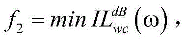
其中,ω表示应用程序中的各IP核映射到光片上网络拓扑结构图上的位置;Among them, ω represents the location where each IP core in the application is mapped to the on-chip network topology diagram;
(2.3)令优化目标的约束条件为:应用程序IP核图中的所有IP核都需要一对一的映射到光片上网络的核心上,表示如下:(2.3) Let the constraints of the optimization objective be: all IP cores in the application IP core map need to be mapped one-to-one to the core of the optical-chip network, which is expressed as follows:


其中,C表示应用程序IP核图中IP核的集合,ci∈C表示C中的第i个IP核,T表示光片上网络拓扑结构图中核心的集合,tj表示T中的第j个核心,Ω:C→T表示IP核映射,Ω(ci)=tj表示将IP核ci映射到光片上网络的核心tj。Among them, C represents the set of IP cores in the application IP core diagram, c i ∈ C represents the ith IP core in C, T represents the set of cores in the network topology diagram on the optical chip, and t j represents the jth in T Ω: C→T represents the IP core mapping, Ω(ci )=t j represents the core t j that maps the IP core ci to the optical-chip network.
(2.4)根据步骤(2.1)、(2.2)和(2.3)的结果,设定映射优化目标为:(2.4) According to the results of steps (2.1), (2.2) and (2.3), set the mapping optimization objective as:

约束条件为:

步骤3,将映射位置ω通过编码的方式表示为个体的染色体。In step 3, the mapped position ω is represented as the chromosome of the individual by means of coding.
(3.1)根据应用程序IP核图共有G个IP核,光片上网络拓扑结构图共有F个核心的参数,将IP核编号为x,且1≤x≤G,将核心编号为y,且1≤y≤F,将映射位置ω表示为一个长度为F的行向量ω;(3.1) According to the application IP core diagram, there are G IP cores, and the network topology diagram on the optical chip has parameters of F cores. The IP cores are numbered as x, and 1≤x≤G, and the cores are numbered as y, and 1 ≤y≤F, express the mapping position ω as a row vector ω of length F;
(3.2)根据IP核映射的位置设置行向量ω各列的值:(3.2) Set the value of each column of the row vector ω according to the location of the IP core mapping:
若编号为x的IP核映射到光片上网络拓扑结构图中的编号为y的核心上,则将ω中的第y列的值设置为x;If the IP core numbered x is mapped to the core numbered y in the on-chip network topology diagram, set the value of the yth column in ω to x;
若核心未被映射到,则将行向量ω中该核心编号对应列的值设置为0。If the core is not mapped to, the value of the column corresponding to the core number in the row vector ω is set to 0.
步骤4,使用NSGS-II算法求解输出最佳映射位置:Step 4, use the NSGS-II algorithm to solve the output optimal mapping position:
参照图2,本步骤的具体实现如下:Referring to Fig. 2, the concrete realization of this step is as follows:
(4.1)设置种群个体数目为N,总迭代次数为K,生成大小为N的初始映射集合O0:(4.1) Set the number of individuals in the population as N, the total number of iterations as K, and generate an initial mapping set O 0 of size N:
(4.1.1)令当前迭代次数k=0,随机生成P个个体,构成父种群Ak;(4.1.1) Set the current iteration number k=0, randomly generate P individuals to form the parent population A k ;
(4.1.2)对父种群Ak进行快速非支配排序,其步骤如下:(4.1.2) Perform fast non-dominated sorting on parent population Ak , the steps are as follows:
第1步,令当前迭代次数h=0;Step 1, let the current iteration number h=0;
第2步,计算父种群Ak中每个个体p的两个参数np和sp,其中np为父种群Ak中支配个体p的个体数,sp为种群中被个体p支配的个体集合;Step 2: Calculate the two parameters n p and s p of each individual p in the parent population Ak , where n p is the number of individuals that dominate the individual p in the parent population Ak , and s p is the population dominated by the individual p. collection of individuals;
所述参数np和sp的计算如下:The parameters n p and sp are calculated as follows:
首先,将个体p的np初始化为0,sp初始化为空集;First, initialize n p of individual p to 0, and sp to the empty set;
其次,将个体p与从父种群Ak中除去个体p外的其余个体i分别进行比较:Second, compare the individual p with the remaining individuals i except the individual p from the parent population Ak :
当且仅当prank>irank或prank=irank且pd<id时,个体i支配个体p,令np=np+1;Individual i dominates individual p if and only if p rank > i rank or p rank = i rank and p d < i d , let n p =n p +1;
当且仅当prank<irank或prank=irank且pd>id时,个体p支配个体i,令sp=sp∪{i};Individual p dominates individual i if and only if p rank < i rank or p rank = i rank and p d > i d , let s p =s p ∪{i};
第3步,找到父种群Ak中所有np为0的个体,并将这些个体移动到非支配层集合Fh中;Step 3: Find all the individuals whose n p is 0 in the parent population Ak , and move these individuals to the non-dominated layer set F h ;
第4步,令非支配层集合Fh中每个个体r的非支配序rrank=h;Step 4, let the non-dominated order r rank =h of each individual r in the non-dominated layer set F h ;
第5步,对于非支配层集合Fh中的每个个体r,遍历被r支配的个体的集合sr中的每个个体l,令nl=nl-1,如果nl=0,则将个体l从种群Ak中移动到临时存储集合H中;Step 5: For each individual r in the non-dominated layer set F h , traverse each individual l in the set s r of individuals dominated by r, let n l =n l -1, if n l =0, Then move the individual l from the population Ak to the temporary storage set H;
第6步,更新迭代次数h,将当前迭代次数h增加1,再将临时存储集合H中的个体移动到新的非支配层集合Fh+1中,为Fh+1中的每个个体r分配非支配序rrank=h+1;Step 6, update the number of iterations h, increase the current number of iterations h by 1, and then move the individuals in the temporary storage set H to the new non-dominated layer set F h+1 , for each individual in F h+1 r allocation non-dominant order r rank = h+1;
第7步,判断父种群Ak是否为空:Step 7, determine whether the parent population Ak is empty:
若父种群Ak为空,则完成快速非支配排序;If the parent population Ak is empty, complete the fast non-dominated sorting;
否则,返回第2步;Otherwise, go back to step 2;
(4.1.3)计算Ak中每个个体p的拥挤度pd,实现如下:(4.1.3) Calculate the crowding degree p d of each individual p in Ak , which is realized as follows:
第一步,记个体p的拥挤度pd,令pd=0,p=1,2,...,N;The first step is to record the crowding degree p d of individual p, let p d =0, p = 1, 2,...,N;
第二步,对于每个个体p,按照个体p对应的目标函数值对种群Ak进行排序,按照排序结果对当前种群中的每个个体p依次标记为1,2,...,N;In the second step, for each individual p, sort the population Ak according to the objective function value corresponding to the individual p, and label each individual p in the current population as 1, 2,...,N in turn according to the sorting result;
第三步,令目标函数值最大和最小的两个个体的拥挤度为无穷大,即1d=Nd=∞;The third step is to make the crowding degree of the two individuals with the largest and smallest objective function values infinite, that is, 1 d =N d =∞;
第四步,通过下式计算个体拥挤度:The fourth step is to calculate the individual crowding degree by the following formula:
pd=pd+(fm(p+1)-fm(p-1))/(fm(N)-fm(1)),p=2,3,...,N-1,m=1,2;p d = p d + (f m (p+1)-f m (p-1))/(f m (N)-f m (1)), p=2,3,...,N- 1, m=1,2;
(4.1.4)从父种群Ak的P个个体中选择Q个个体进行交叉变异,生成大小为P的子种群Bk,P>Q;(4.1.4) Select Q individuals from the P individuals of the parent population A k to perform crossover mutation, and generate a subpopulation B k of size P, P>Q;
所述的从父种群Ak中选择Q个个体,是优先选择非支配序小的个体,即首先选取非支配序最小的个体,再将当前已选择的个体数目与需要选择的个体数目Q进行比较:The selection of Q individuals from the parent population Ak is to preferentially select the individuals with the smallest non-dominant order, that is, first select the individual with the smallest non-dominant order, and then compare the number of currently selected individuals with the number of individuals to be selected Q. Compare:
如果已选择的个体数目小于Q,则继续选择次小的非支配序的个体;If the number of selected individuals is less than Q, continue to select the next-smallest non-dominated individuals;
如果当前已选择的个体总数目大于Q,则将最后一次选择的非支配序为x的所有个体按照拥挤度进行从大到小排序,并依次选择拥挤度大的个体,直到选出的个体数目等于Q为止;If the total number of currently selected individuals is greater than Q, sort all the individuals whose non-dominant order is x in the last selection in descending order according to the degree of crowding, and select the individuals with the largest degree of crowding in turn, until the number of selected individuals is reached until it is equal to Q;
(4.1.5)合并父种群Ak与子种群Bk,得到大小为2P的联合种群Ck;(4.1.5) Merge parent population A k and child population B k to obtain a combined population C k of size 2P;
(4.1.6)对联合种群Ck进行快速非支配排序,并计算Ck中每个个体c的拥挤度cd,其中快速非支配排序的实现与(4.1.2)相同,拥挤度的计算与(4.1.3)相同;(4.1.6) Perform fast non-dominated sorting on the joint population C k , and calculate the crowding degree c d of each individual c in C k , where the implementation of fast non-dominated sorting is the same as (4.1.2), the calculation of the crowding degree Same as (4.1.3);
(4.1.7)更新迭代次数k,将当前迭代次数k增加1;(4.1.7) Update the number of iterations k, and increase the current number of iterations k by 1;
从联合种群Ck中选择P+n个个体,构成新的父种群Ak+1,更新新的父种群Ak+1的大小P,即将P增加n,其中选择过程与(4.1.4)相同;Select P+n individuals from the combined population C k to form a new parent population A k+1 , update the size P of the new parent population A k+1 , that is, increase P by n, where the selection process is the same as (4.1.4) same;
(4.1.8)将新的父种群Ak+1中的个体数目P+n与需要生成的初始种群O0的大小N进行比较:(4.1.8) Compare the number of individuals P+n in the new parent population A k+1 with the size N of the initial population O 0 to be generated:
若P+n≥N,则对父种群Ak+1进行快速非支配排序,并计算Ak+1中每个个体a的拥挤度ad,从P+n个个体中选择N个个体作为初始种群O0,其中快速非支配排序的实现与(4.1.2)相同,拥挤度的计算与(4.1.3)相同,选择过程与(4.1.4)相同,生成初始种群O0结束;If P+n≥N, perform fast non-dominated sorting on the parent population A k+1 , and calculate the crowding degree a d of each individual a in A k+1 , and select N individuals from P+n individuals as Initial population O 0 , in which the implementation of fast non-dominated sorting is the same as (4.1.2), the calculation of crowding degree is the same as (4.1.3), and the selection process is the same as (4.1.4), and the generation of initial population O 0 ends;
若P+n<N,则更新进行交叉变异的个体数Q,将Q增加m,并返回(4.1.2)。If P+n<N, update the number of individuals Q for cross-mutation, increase Q by m, and return to (4.1.2).
(4.2)对O0中的个体进行快速非支配排序,其中快速非支配排序的实现与(4.1.2)相同;(4.2) Perform fast non-dominated sorting on the individuals in O 0 , where the implementation of fast non-dominated sorting is the same as (4.1.2);
(4.3)计算中O0每个个体n的拥挤度nd,其中拥挤度的计算与(4.1.3)相同;(4.3) Crowding degree nd of each individual n of O 0 in the calculation, wherein the calculation of crowding degree is the same as (4.1.3);
(4.4)令迭代次数t=0;(4.4) Let the number of iterations t=0;
(4.5)从父种群Ot中选择M个个体,并依次进行交叉、变异,产生大小为N的子种群Yt,其中M<N,选择过程与(4.1.4)相同;(4.5) Select M individuals from the parent population O t , and perform crossover and mutation in turn to generate a sub-population Y t of size N, where M<N, the selection process is the same as (4.1.4);
(4.6)对父种群Ot与子种群Yt进行合并,产生大小为2N的组合种群Rt;(4.6) Merge the parent population O t and the child population Y t to generate a combined population R t with a size of 2N;
(4.7)对组合种群Rt中的个体进行快速非支配排序,计算每个个体r的拥挤度rd,并选出N个个体,组成大小为N的新一代种群Ot+1,其中快速非支配排序的实现与(4.1.2)相同,拥挤度的计算与(4.1.3)相同,选择过程与(4.1.4)相同;(4.7) Perform fast non-dominated sorting on the individuals in the combined population R t , calculate the crowding degree r d of each individual r, and select N individuals to form a new generation population O t+1 of size N, in which the fast The implementation of non-dominated sorting is the same as (4.1.2), the calculation of crowding degree is the same as (4.1.3), and the selection process is the same as (4.1.4);
(4.8)将当前迭代次数t与设定的总迭代次数K进行比较:(4.8) Compare the current iteration number t with the set total iteration number K:
若t<K,返回(4.5);If t<K, return (4.5);
若t=K,输出最佳映射位置集合ω*。即可在给定的应用程序IP核图和光片上网络拓扑结构图上,按照最佳映射位置集合ω*进行IP核映,能得到最佳映射结果,实现通过IP核映射对光片上网络的串扰噪声与插入损耗进行优化的目标。If t=K, output the best mapping position set ω * . That is, on the given application IP core map and optical on-chip network topology diagram, IP core mapping is performed according to the optimal mapping position set ω * , and the best mapping result can be obtained, realizing the crosstalk to the optical on-chip network through IP core mapping. Noise and insertion loss optimization goals.
以上描述仅是本发明的一个具体实例,并未构成对本发明的任何限制,显然对于本领域的专业技术人员来说,在了解了本发明内容和原理后,都可能在不背离本发明原理、结构的情况下,进行形式和细节上的各种修改和改变,但是这些基于本发明思想的修正和改变仍在本发明的权利要求保护范围之内。The above description is only a specific example of the present invention, and does not constitute any limitation to the present invention. Obviously, for those skilled in the art, after understanding the content and principles of the present invention, they may not deviate from the principles of the present invention, In the case of the structure, various modifications and changes in form and details are made, but these modifications and changes based on the idea of the present invention are still within the scope of protection of the claims of the present invention.
Claims (10)


Priority Applications (1)
| Application Number | Priority Date | Filing Date | Title |
|---|---|---|---|
| CN202010505518.6A CN111752891B (en) | 2020-06-05 | 2020-06-05 | IP core mapping method for optical network on chip |
Applications Claiming Priority (1)
| Application Number | Priority Date | Filing Date | Title |
|---|---|---|---|
| CN202010505518.6A CN111752891B (en) | 2020-06-05 | 2020-06-05 | IP core mapping method for optical network on chip |
Publications (2)
| Publication Number | Publication Date |
|---|---|
| CN111752891A true CN111752891A (en) | 2020-10-09 |
| CN111752891B CN111752891B (en) | 2022-06-03 |
Family
ID=72674755
Family Applications (1)
| Application Number | Title | Priority Date | Filing Date |
|---|---|---|---|
| CN202010505518.6A Active CN111752891B (en) | 2020-06-05 | 2020-06-05 | IP core mapping method for optical network on chip |
Country Status (1)
| Country | Link |
|---|---|
| CN (1) | CN111752891B (en) |
Cited By (11)
| Publication number | Priority date | Publication date | Assignee | Title |
|---|---|---|---|---|
| CN113986812A (en) * | 2021-09-07 | 2022-01-28 | 西安电子科技大学 | Optical on-chip network mapping method and device based on CHNN |
| CN115276820A (en) * | 2022-07-29 | 2022-11-01 | 西安电子科技大学 | Method for setting power gradient of on-chip optical interconnection light source with mapping assistance |
| US11817903B2 (en) | 2020-08-06 | 2023-11-14 | Celestial Ai Inc. | Coherent photonic computing architectures |
| US11835777B2 (en) | 2022-03-18 | 2023-12-05 | Celestial Ai Inc. | Optical multi-die interconnect bridge (OMIB) |
| US12191257B2 (en) | 2022-07-26 | 2025-01-07 | Celestial Ai Inc. | Electrical bridge package with integrated off-bridge photonic channel interface |
| US12217056B2 (en) | 2023-01-27 | 2025-02-04 | Celestial Ai Inc. | Load/store unit for a tensor engine and methods for loading or storing a tensor |
| US12259575B2 (en) | 2021-06-18 | 2025-03-25 | Celestial Ai Inc. | Clock signal distribution using photonic fabric |
| US12271595B2 (en) | 2022-03-18 | 2025-04-08 | Celestial Ai Inc. | Photonic memory fabric for system memory interconnection |
| US12283584B2 (en) | 2022-07-26 | 2025-04-22 | Celestial Ai Inc. | Electrical bridge package with integrated off-bridge photonic channel interface |
| US12353988B2 (en) | 2020-07-09 | 2025-07-08 | Celestial Ai Inc. | Neuromorphic photonics with coherent linear neurons |
| US12436346B2 (en) | 2022-03-18 | 2025-10-07 | Celestial Ai Inc. | Optically bridged multicomponent package with extended temperature range |
Citations (7)
| Publication number | Priority date | Publication date | Assignee | Title |
|---|---|---|---|---|
| CN102202005A (en) * | 2011-07-12 | 2011-09-28 | 西安电子科技大学 | Reconfigurable network on mating plate and configuration method |
| KR101382606B1 (en) * | 2013-06-10 | 2014-04-07 | 성균관대학교산학협력단 | Apparatus and method for task mapping of hybrid optical networks on chip and hybrid optical networks on chip system using the same |
| CN106416110A (en) * | 2014-05-28 | 2017-02-15 | 华为技术有限公司 | Scalable silicon photonic switching architectures for optical networks |
| CN107769856A (en) * | 2016-08-22 | 2018-03-06 | 中兴通讯股份有限公司 | A kind of optical signal sends system, reception system and method and communication system |
| US20180167159A1 (en) * | 2009-12-08 | 2018-06-14 | Snell Holdings, Llc | Optical Subchannel Routing, Protection Switching and Security |
| CN108737011A (en) * | 2018-06-15 | 2018-11-02 | 西安电子科技大学 | The Wavelength allocation method of reduction crosstalk based on ant group algorithm |
| CN110383254A (en) * | 2016-12-01 | 2019-10-25 | 安培计算有限责任公司 | Optimize memory maps associated with network nodes |
-
2020
- 2020-06-05 CN CN202010505518.6A patent/CN111752891B/en active Active
Patent Citations (7)
| Publication number | Priority date | Publication date | Assignee | Title |
|---|---|---|---|---|
| US20180167159A1 (en) * | 2009-12-08 | 2018-06-14 | Snell Holdings, Llc | Optical Subchannel Routing, Protection Switching and Security |
| CN102202005A (en) * | 2011-07-12 | 2011-09-28 | 西安电子科技大学 | Reconfigurable network on mating plate and configuration method |
| KR101382606B1 (en) * | 2013-06-10 | 2014-04-07 | 성균관대학교산학협력단 | Apparatus and method for task mapping of hybrid optical networks on chip and hybrid optical networks on chip system using the same |
| CN106416110A (en) * | 2014-05-28 | 2017-02-15 | 华为技术有限公司 | Scalable silicon photonic switching architectures for optical networks |
| CN107769856A (en) * | 2016-08-22 | 2018-03-06 | 中兴通讯股份有限公司 | A kind of optical signal sends system, reception system and method and communication system |
| CN110383254A (en) * | 2016-12-01 | 2019-10-25 | 安培计算有限责任公司 | Optimize memory maps associated with network nodes |
| CN108737011A (en) * | 2018-06-15 | 2018-11-02 | 西安电子科技大学 | The Wavelength allocation method of reduction crosstalk based on ant group algorithm |
Non-Patent Citations (1)
| Title |
|---|
| HUAXI GU等: "A Reliability-Aware Joint Design Method of Application Mapping and Wavelength Assignment for WDM-Based Silicon Photonic Interconnects on Chip", 《DIGITAL OBJECT IDENTIFIER》 * |
Cited By (26)
| Publication number | Priority date | Publication date | Assignee | Title |
|---|---|---|---|---|
| US12353988B2 (en) | 2020-07-09 | 2025-07-08 | Celestial Ai Inc. | Neuromorphic photonics with coherent linear neurons |
| US11817903B2 (en) | 2020-08-06 | 2023-11-14 | Celestial Ai Inc. | Coherent photonic computing architectures |
| US12353006B2 (en) | 2021-06-18 | 2025-07-08 | Celestial Ai Inc. | Electro-photonic network for machine learning |
| US12259575B2 (en) | 2021-06-18 | 2025-03-25 | Celestial Ai Inc. | Clock signal distribution using photonic fabric |
| US12339490B2 (en) | 2021-06-18 | 2025-06-24 | Celestial Ai Inc. | Clock signal distribution using photonic fabric |
| CN113986812A (en) * | 2021-09-07 | 2022-01-28 | 西安电子科技大学 | Optical on-chip network mapping method and device based on CHNN |
| US12242122B2 (en) | 2022-03-18 | 2025-03-04 | Celestial Ai Inc. | Multicomponent photonically intra-die bridged assembly |
| US12164162B2 (en) | 2022-03-18 | 2024-12-10 | Celestial Ai Inc. | Multicomponent photonically bridged assembly |
| US12271595B2 (en) | 2022-03-18 | 2025-04-08 | Celestial Ai Inc. | Photonic memory fabric for system memory interconnection |
| US12468103B2 (en) | 2022-03-18 | 2025-11-11 | Celestial Ai Inc. | Optically bridged multicomponent package with extended temperature range |
| US12216318B2 (en) | 2022-03-18 | 2025-02-04 | Celestial Ai Inc. | Optical bridging element for separately stacked electrical ICs |
| US12442998B2 (en) | 2022-03-18 | 2025-10-14 | Celestial AI, Inc. | Optically bridged multicomponent package with extended temperature range |
| US12443000B2 (en) | 2022-03-18 | 2025-10-14 | Celestial Ai Inc. | Optically bridged multicomponent package with extended temperature range |
| US12164161B1 (en) | 2022-03-18 | 2024-12-10 | Celestial Ai Inc. | Stacked-dies optically bridged multicomponent package |
| US12124095B2 (en) | 2022-03-18 | 2024-10-22 | Celestial Ai Inc. | Optical multi-die interconnect bridge with optical interface |
| US12298608B1 (en) | 2022-03-18 | 2025-05-13 | Celestial Ai Inc. | Optically bridged multicomponent package with extended temperature range |
| US11835777B2 (en) | 2022-03-18 | 2023-12-05 | Celestial Ai Inc. | Optical multi-die interconnect bridge (OMIB) |
| US12442999B2 (en) | 2022-03-18 | 2025-10-14 | Celestial Ai Inc. | Optically bridged multicomponent package with extended temperature range |
| US12442997B2 (en) | 2022-03-18 | 2025-10-14 | Celestial AI, Inc. | Optically bridged multicomponent package with extended temperature range |
| US12399333B2 (en) | 2022-03-18 | 2025-08-26 | Celestial AI, Inc. | Optical multi-die interconnect bridge with electrical and optical interfaces |
| US12436346B2 (en) | 2022-03-18 | 2025-10-07 | Celestial Ai Inc. | Optically bridged multicomponent package with extended temperature range |
| US12191257B2 (en) | 2022-07-26 | 2025-01-07 | Celestial Ai Inc. | Electrical bridge package with integrated off-bridge photonic channel interface |
| US12283584B2 (en) | 2022-07-26 | 2025-04-22 | Celestial Ai Inc. | Electrical bridge package with integrated off-bridge photonic channel interface |
| CN115276820A (en) * | 2022-07-29 | 2022-11-01 | 西安电子科技大学 | Method for setting power gradient of on-chip optical interconnection light source with mapping assistance |
| CN115276820B (en) * | 2022-07-29 | 2023-09-01 | 西安电子科技大学 | On-chip optical interconnection light source power gradient setting method using mapping assistance |
| US12217056B2 (en) | 2023-01-27 | 2025-02-04 | Celestial Ai Inc. | Load/store unit for a tensor engine and methods for loading or storing a tensor |
Also Published As
| Publication number | Publication date |
|---|---|
| CN111752891B (en) | 2022-06-03 |
Similar Documents
| Publication | Publication Date | Title |
|---|---|---|
| CN111752891B (en) | IP core mapping method for optical network on chip | |
| CN103826219B (en) | A Power Allocation Method for Secrecy System with Guaranteed Delay QoS Requirements | |
| CN110709866A (en) | multimodal reservoir | |
| CN104092606B (en) | Energy-saving routing method based on service duration time scheduling in optical network | |
| CN113673677B (en) | Method, equipment and medium for realizing nonlinear activation function RELU | |
| TWI426383B (en) | Estimation method to evaluate a system reliability of a cloud computing network | |
| CN107343303B (en) | Based on the routing optimization method of Duality Decomposition in wireless Mesh netword | |
| CN104092609A (en) | A method and device for constructing an IP over WDM network | |
| Yao et al. | Thermal-sensitive design and power optimization for a 3D torus-based optical NoC | |
| Li et al. | Performance of Rotation‐Symmetric Bosonic Codes in a Quantum Repeater Network | |
| Xie et al. | Performance optimization and evaluation for torus-based optical networks-on-chip | |
| CN103236982B (en) | A kind of how point-to-multipoint smooth multicast route method based on multinuclear | |
| Liu et al. | SL-Hyper-FleX: a cognitive and flexible-bandwidth optical datacom network by self-supervised learning | |
| CN105591876A (en) | A virtual network mapping method | |
| CN109302647A (en) | Spectrum allocation method, device and storage medium | |
| CN110059938B (en) | Power distribution network planning method based on association rule driving | |
| Yan et al. | A novel algorithm for reducing the power loss of routing paths in ONoCs | |
| CN115729012A (en) | Topological resonant cavity and preparation method of high-dimensional energy-time entanglement source | |
| CN115276820A (en) | Method for setting power gradient of on-chip optical interconnection light source with mapping assistance | |
| CN117236450B (en) | Quantum entanglement resource scheduling method and device and electronic equipment | |
| CN103346965B (en) | Based on the light multicast route method of coding subgraph Optimized Coding Based cost | |
| CN117236453A (en) | Quantum entanglement resource scheduling method, device and electronic equipment | |
| CN101383759A (en) | A Protection Method for Dividing Management Areas in Optical Networks | |
| CN116562384B (en) | Fredkin quantum logic gate | |
| Cheng et al. | Minimizing worst-case data transmission cycles in wavelength-routed optical noc through bandwidth allocation |
Legal Events
| Date | Code | Title | Description |
|---|---|---|---|
| PB01 | Publication | ||
| PB01 | Publication | ||
| SE01 | Entry into force of request for substantive examination | ||
| SE01 | Entry into force of request for substantive examination | ||
| GR01 | Patent grant | ||
| GR01 | Patent grant |