CN111668112A - Semiconductor packaging method - Google Patents
Semiconductor packaging method Download PDFInfo
- Publication number
- CN111668112A CN111668112A CN201910176975.2A CN201910176975A CN111668112A CN 111668112 A CN111668112 A CN 111668112A CN 201910176975 A CN201910176975 A CN 201910176975A CN 111668112 A CN111668112 A CN 111668112A
- Authority
- CN
- China
- Prior art keywords
- elastic
- spacer
- carrier board
- packaged
- semiconductor packaging
- Prior art date
- Legal status (The legal status is an assumption and is not a legal conclusion. Google has not performed a legal analysis and makes no representation as to the accuracy of the status listed.)
- Pending
Links
Images


Classifications
-
- H10W74/01—
-
- H10W42/00—
-
- H10W74/00—
Landscapes
- Encapsulation Of And Coatings For Semiconductor Or Solid State Devices (AREA)
- Structures Or Materials For Encapsulating Or Coating Semiconductor Devices Or Solid State Devices (AREA)
Abstract
Description
技术领域technical field
本申请涉及一种半导体技术领域,尤其涉及一种半导体封装方法。The present application relates to the technical field of semiconductors, and in particular, to a semiconductor packaging method.
背景技术Background technique
常见的半导体封装技术,比如芯片封装技术主要包含下述工艺过程:首先将裸片正面通过胶带粘接在载板上,进行热压塑封,然后将载板剥离,在裸片正面进行再布线工艺,形成再布线结构,并进行封装。Common semiconductor packaging technology, such as chip packaging technology, mainly includes the following process: first, the front side of the bare chip is bonded to the carrier board by tape, and then hot-pressed and plastic-sealed, then the carrier board is peeled off, and the front side of the bare chip is re-wiring process. , forming a re-wiring structure, and encapsulating it.
然而,在热压塑封之后,模压成型后的成型产品容易出现翘曲,尤其是在面板级封装工艺中,翘曲现象更容易出现,使得在后续的再布线工艺中,难以定位裸片的精确位置,从而对再布线工艺产生很大影响,甚至使得再布线工艺难以进行。However, after thermocompression molding, the molded product after molding is prone to warpage, especially in the panel-level packaging process, the warpage phenomenon is more likely to occur, making it difficult to position the die accurately in the subsequent rewiring process. position, which greatly affects the re-wiring process, and even makes the re-wiring process difficult to carry out.
发明内容SUMMARY OF THE INVENTION
本申请的一个方面提供一种半导体封装方法,包括:One aspect of the present application provides a semiconductor packaging method, comprising:
在载板上划分多个贴装区和空白区,所述空白区位于至少两个相邻的贴装区之间,将多个待封装芯片贴装于所述多个贴装区,并将弹性隔离件设于所述空白区;其中,所述多个待封装芯片的正面朝向所述载板;A plurality of mounting areas and blank areas are divided on the carrier board, the blank areas are located between at least two adjacent mounting areas, a plurality of chips to be packaged are mounted on the multiple mounting areas, and The elastic spacer is arranged in the blank area; wherein, the front surfaces of the plurality of chips to be packaged face the carrier board;
形成包封层,所述包封层覆盖在所述载板上,且所述包封层用于包封住所述多个待封装芯片及所述弹性隔离件。An encapsulation layer is formed, the encapsulation layer covers the carrier board, and the encapsulation layer is used to encapsulate the plurality of chips to be packaged and the elastic spacer.
可选的,所述弹性隔离件的材料包括硅橡胶。Optionally, the material of the elastic spacer includes silicone rubber.
可选的,所述弹性隔离件的厚度小于所述包封层的厚度。Optionally, the thickness of the elastic spacer is smaller than the thickness of the encapsulation layer.
可选的,所述弹性隔离件的厚度D1与所述包封层的厚度D满足:0.4D<D1<0.9D。Optionally, the thickness D1 of the elastic spacer and the thickness D of the encapsulation layer satisfy: 0.4D<D1<0.9D.
可选的,所述弹性隔离件的厚度D1与所述包封层的厚度D满足:D1=2/3D。Optionally, the thickness D1 of the elastic spacer and the thickness D of the encapsulation layer satisfy: D1=2/3D.
可选的,所述弹性隔离件的厚度D1满足:400μm≤D1≤800μm。Optionally, the thickness D1 of the elastic spacer satisfies: 400 μm≤D1≤800 μm.
可选的,所述弹性隔离件包括沿一个方向延伸的条状隔离部;或,Optionally, the elastic spacer includes a strip-shaped spacer extending in one direction; or,
所述弹性隔离件包括多个隔离部。The elastic spacer includes a plurality of spacers.
可选的,所述弹性隔离件包括多个隔离部时,所述弹性隔离件包括沿所述载板的宽度方向延伸的第一隔离部和沿所述载板的长度方向延伸的第二隔离部,所述弹性隔离件的第一隔离部和第二隔离部交叉连接,且所述第一隔离部的长度与所述载板的宽度相同,所述第二隔离部的长度与所述载板的长度相同。Optionally, when the elastic spacer includes a plurality of spacers, the elastic spacer includes a first spacer extending along the width direction of the carrier plate and a second spacer extending along the length direction of the support plate. The first isolation part and the second isolation part of the elastic spacer are cross-connected, and the length of the first isolation part is the same as the width of the carrier plate, and the length of the second isolation part is the same as that of the carrier board. The boards are the same length.
可选的,所述弹性隔离件包括多个隔离部时,所述多个隔离部中至少两个交叉连接,且至少一个隔离部沿偏离所述载板的宽度方向且偏离所述载板的长度方向的方向延伸。Optionally, when the elastic spacer includes multiple isolation parts, at least two of the multiple isolation parts are cross-connected, and at least one isolation part deviates from the width direction of the carrier board and deviates from the carrier board. Extends in the direction of the length direction.
可选的,所述弹性隔离件的制作方法为:Optionally, the manufacturing method of the elastic spacer is:
热压成型弹性裸板;Thermoforming elastic bare board;
剪裁弹性裸板,所剪裁掉的区域对应于所述载板上的所述贴装区。The elastic bare board is trimmed, and the trimmed area corresponds to the mounting area on the carrier board.
可选的,在形成包封层之后,所述方法包括:Optionally, after forming the encapsulation layer, the method includes:
剥离所述载板,露出所述多个待封装芯片的正面;peeling off the carrier to expose the front surfaces of the plurality of chips to be packaged;
在所述芯片的正面形成再布线结构,所述再布线结构用于将所述芯片的正面的焊垫引出。A redistribution structure is formed on the front surface of the chip, and the redistribution structure is used to lead out the bonding pads on the front surface of the chip.
可选的,在所述形成包封层之后,剥离所述载板之前,所述方法包括在所述包封层远离所述载板的第一表面贴装支撑板;Optionally, after forming the encapsulation layer and before peeling off the carrier board, the method includes mounting a support plate on a first surface of the encapsulation layer away from the carrier board;
在所述芯片的正面形成再布线结构之后,所述方法包括剥离所述支撑板。After forming a redistribution structure on the front side of the chip, the method includes peeling off the support plate.
本申请实施例提供的上述半导体封装方法,通过弹性隔离件的设置,使得在包封贴装区及空白区的包封层所形成的较大面积的面板中具有弹性隔离件,从而使得整个较大面积的面板具有良好的弹性,进而降低包封层及整个塑封产品的翘曲程度,保证封装的成功率及产品的良率。In the above-mentioned semiconductor packaging method provided by the embodiments of the present application, through the arrangement of elastic spacers, elastic spacers are provided in the large-area panel formed by the encapsulation layer that encapsulates the mounting area and the blank area, so that the entire larger area is provided with elastic spacers. The large-area panel has good elasticity, thereby reducing the warpage of the encapsulation layer and the entire plastic-encapsulated product, ensuring the success rate of packaging and the yield of the product.
附图说明Description of drawings
图1(a)是现有技术中的裸片受到模塑树脂材料的作用力时的结构示意图。FIG. 1( a ) is a schematic structural diagram of a bare chip in the prior art when it is subjected to a force of a molding resin material.
图1(b)是热压塑封之后的成型产品产生翘曲的结构示意图。Figure 1(b) is a schematic structural diagram of the warpage of the molded product after thermocompression and plastic sealing.
图2是根据本公开一实例性实施例提出的半导体封装方法的流程图。FIG. 2 is a flowchart of a semiconductor packaging method according to an exemplary embodiment of the present disclosure.
图3(a)-图3(g)是根据本公开一示例性实施例中半导体封装方法的工艺流程图。3(a)-3(g) are process flow diagrams of a semiconductor packaging method according to an exemplary embodiment of the present disclosure.
图4(a)是根据本公开一示例性实施例提出的弹性裸板的正面结构示意图。FIG. 4( a ) is a schematic diagram of a front structure of an elastic bare board according to an exemplary embodiment of the present disclosure.
图4(b)是根据本公开一示例性实施例提出的弹性隔离件的制作示意图。FIG. 4( b ) is a schematic diagram of the fabrication of an elastic spacer according to an exemplary embodiment of the present disclosure.
图4(c)是根据本公开一示例性实施例提出的载板的正面结构示意图。FIG. 4( c ) is a schematic diagram of a front structure of a carrier board according to an exemplary embodiment of the present disclosure.
图4(d)是根据本公开一示例性实施例提出的载板和弹性隔离件的正面结构示意图。FIG. 4(d) is a schematic diagram of the front structure of the carrier plate and the elastic spacer according to an exemplary embodiment of the present disclosure.
图4(e)是根据本公开另一示例性实施例提出的弹性隔离件的制作示意图。FIG. 4(e) is a schematic diagram of the fabrication of an elastic spacer according to another exemplary embodiment of the present disclosure.
图5是根据本公开一示例性实施例提供的具有支撑板的半导体封装结构的结构示意图。FIG. 5 is a schematic structural diagram of a semiconductor package structure with a support plate provided according to an exemplary embodiment of the present disclosure.
图6是根据本公开一示例性实施例提供的在晶圆表面设置保护层及切分晶圆的示意图。FIG. 6 is a schematic diagram of disposing a protective layer on a wafer surface and dicing the wafer according to an exemplary embodiment of the present disclosure.
图7是根据本公开一示例性实施例提供的保护层设有开口的半导体封装结构的结构示意图。FIG. 7 is a schematic structural diagram of a semiconductor package structure provided with an opening in a protective layer according to an exemplary embodiment of the present disclosure.
具体实施方式Detailed ways
这里将详细地对示例性实施例进行说明,其示例表示在附图中。下面的描述涉及附图时,除非另有表示,不同附图中的相同数字表示相同或相似的要素。以下示例性实施例中所描述的实施方式并不代表与本申请相一致的所有实施方式。相反,它们仅是与如所附权利要求书中所详述的、本申请的一些方面相一致的装置和方法的例子。Exemplary embodiments will be described in detail herein, examples of which are illustrated in the accompanying drawings. Where the following description refers to the drawings, the same numerals in different drawings refer to the same or similar elements unless otherwise indicated. The implementations described in the illustrative examples below are not intended to represent all implementations consistent with this application. Rather, they are merely examples of apparatus and methods consistent with some aspects of the present application as recited in the appended claims.
在本申请使用的术语是仅仅出于描述特定实施例的目的,而非旨在限制本申请。除非另作定义,本申请使用的技术术语或者科学术语应当为本发明所属领域内具有一般技能的人士所理解的通常意义。本申请说明书以及权利要求书中使用的“一个”或者“一”等类似词语也不表示数量限制,而是表示存在至少一个。“多个”表示两个或两个以上。“包括”或者“包含”等类似词语意指出现在“包括”或者“包含”前面的元件或者物件涵盖出现在“包括”或者“包含”后面列举的元件或者物件及其等同,并不排除其他元件或者物件。“连接”或者“相连”等类似的词语并非限定于物理的或者机械的连接,而且可以包括电性的连接,不管是直接的还是间接的。“上”和/或“下”等类似词语只是为了便于说明,而并非限于一个位置或者一种空间定向。在本申请说明书和所附权利要求书中所使用的单数形式的“一种”、“所述”和“该”也旨在包括多数形式,除非上下文清楚地表示其他含义。还应当理解,本文中使用的术语“和/或”是指并包含一个或多个相关联的列出项目的任何或所有可能组合。The terminology used in this application is for the purpose of describing particular embodiments only and is not intended to limit the application. Unless otherwise defined, technical or scientific terms used in this application shall have the ordinary meaning as understood by those of ordinary skill in the art to which this invention belongs. Words like "a" or "an" used in the specification and claims of this application also do not denote a quantitative limitation, but rather denote the presence of at least one. "Plurality" means two or more. Words like "include" or "include" mean that the elements or items appearing before "including" or "including" cover the elements or items listed after "including" or "including" and their equivalents, and do not exclude other elements or objects. "Connected" or "connected" and similar words are not limited to physical or mechanical connections, but may include electrical connections, whether direct or indirect. Words like "upper" and/or "lower" are for convenience of description and are not limited to one position or one spatial orientation. As used in this specification and the appended claims, the singular forms "a," "the," and "the" are intended to include the plural forms as well, unless the context clearly dictates otherwise. It will also be understood that the term "and/or" as used herein refers to and includes any and all possible combinations of one or more of the associated listed items.
在封装过程中,芯片的正面贴装于载板上后,在对芯片的背面进行包封时,通常需要高压高温成型的方式形成包封层(即热压塑封),在热压塑封之后,模压成型后的成型产品容易出现翘曲,而使芯片偏离预定粘接位置从而影响后期的布线工艺。请参考图1(a)和图1(b)所示,发明人(们)经过研究发现,对于面板级封装,在热压成型工艺中,由于钢性载板200和包封层204材料的热膨胀系数之间的差异,在升温及降温过程中,载板和包封材料膨胀和收缩的程度不同;且成型的包封材料即包封层204在热压过程中,在常温条件下急速升温到热压温度的急速升温过程中,以及在之后的降温过程中,材料内部积累了大量作用力F(如图1(a)所示),使得模塑成型后的成型产品出现翘曲现象(如图1(b)所示)。由于翘曲现象的产生,使得后续的布线工艺中,难以定位芯片201在载板200中的精确位置,对布线工艺产生很大影响,甚至使得布线工艺难以进行。特别的,在大型载板中,由于载板的尺寸较大,即便是轻微的载板翘曲,也会使载板200远离中心的外部四周围部分的芯片201相对于模塑成型之前,产生较大尺寸的位置变化。因而,在大型载板封装工艺中,解决模压成型的翘曲问题成为整个工艺的关键之一,翘曲问题甚至限制了载板尺寸的放大化发展,成为大尺寸载板封装中的技术壁垒。In the packaging process, after the front side of the chip is mounted on the carrier board, when the back side of the chip is encapsulated, it is usually necessary to form an encapsulation layer by high pressure and high temperature molding (ie, hot compression molding). The molded product after compression molding is prone to warpage, which makes the chip deviate from the predetermined bonding position and affects the later wiring process. Please refer to FIG. 1( a ) and FIG. 1( b ), the inventor(s) found through research that for panel-level packaging, in the thermoforming process, due to the The difference between the thermal expansion coefficients, in the process of heating and cooling, the expansion and contraction of the carrier plate and the encapsulation material are different; and the encapsulation material that is formed, that is, the
为了解决面板级封装工艺中的上述问题,本申请提供了一种半导体封装方法。在封装过程中,在载板上划分多个贴装区和空白区,所述空白区位于至少两个相邻的贴装区之间,将多个待封装芯片贴装于所述多个贴装区,并将弹性隔离件设于所述空白区;其中,所述多个待封装芯片的正面朝向所述载板;在载板之上对待封装芯片进行封装,形成包封层,即包封层覆盖在所述载板上且包封住所述多个待封装芯片及所述弹性隔离件。本公开的上述实施方式,通过弹性隔离件的设置,使得在包封贴装区及空白区的包封层所形成的较大面积的面板中具有弹性隔离件,从而使得整个较大面积的面板具有良好的弹性,进而降低包封层及整个塑封产品的翘曲程度,保证裸片的定位,保证封装的成功率及产品的良率。In order to solve the above problems in the panel level packaging process, the present application provides a semiconductor packaging method. During the packaging process, a plurality of mounting areas and blank areas are divided on the carrier board, the blank areas are located between at least two adjacent mounting areas, and multiple chips to be packaged are mounted on the multiple mounting areas. The packaging area is installed, and elastic spacers are arranged in the blank area; wherein, the front surfaces of the plurality of chips to be packaged face the carrier board; the chips to be packaged are packaged on the carrier board to form an encapsulation layer, that is, a package layer. The encapsulation layer covers the carrier board and encapsulates the plurality of chips to be packaged and the elastic spacer. In the above-mentioned embodiments of the present disclosure, through the provision of elastic spacers, elastic spacers are provided in the larger-area panel formed by the encapsulation layer that encapsulates the mounting area and the blank area, so that the entire larger-area panel can be provided with elastic spacers. It has good elasticity, thereby reducing the warpage of the encapsulation layer and the entire plastic encapsulation product, ensuring the positioning of the bare chip, and ensuring the success rate of packaging and product yield.
如图2、图3(a)-图3(g)、图4(a)-图4(e)、图5、图6和图7所示,本公开提供一种半导体封装方法及半导体封装结构。As shown in FIG. 2, FIG. 3(a)-FIG. 3(g), FIG. 4(a)-FIG. 4(e), FIG. 5, FIG. 6 and FIG. 7, the present disclosure provides a semiconductor packaging method and semiconductor package structure.
图2是根据本公开一实例性实施例提出的半导体封装方法的流程图。如图2所示,半导体封装方法包括下述步骤101和步骤102:FIG. 2 is a flowchart of a semiconductor packaging method according to an exemplary embodiment of the present disclosure. As shown in FIG. 2, the semiconductor packaging method includes the following
在步骤101中,在载板上划分多个贴装区和空白区,所述空白区位于至少两个相邻的贴装区之间,将多个待封装芯片贴装于所述多个贴装区,并将弹性隔离件设于所述空白区;其中,所述多个待封装芯片的正面朝向所述载板。In
在一实施例中,载板200的形状可包括:圆形、矩形或其他形状,本实施例中的载板200的形状为矩形。载板200可以是大尺寸的不锈钢板、聚合物基板等。所述待封装芯片201的正面朝向所述载板200。In one embodiment, the shape of the
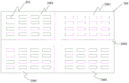
如图3(a)所示,在载板200上划分4个贴装区2001和空白区2002。其中,空白区2002包括横向延伸的一部分和纵向延伸的另一部分,该横向延伸的部分空白区和纵向延伸的部分空白区共同将载板200分隔为4个贴装区。As shown in FIG. 3( a ), the
如图3(b)所示,将弹性隔离件300放置于载板200上的空白区2002,弹性隔离件300包括沿载板200的宽度方向延伸(即纵向延伸)的第一隔离部302和沿载板200的长度方向延伸(即横向延伸)的第二隔离部301。其中,弹性隔离件的第一隔离部302和第二隔离部301交叉连接。从而使得弹性隔离件300通过第一隔离部302和第二隔离部301将载板200上的区域划分成4个小区域(即贴装区2001)。As shown in FIG. 3( b ), the
第一隔离部302的长度与载板200的宽度可大致相同,第二隔离部301的长度与载板200的长度也可大致相同。这样,弹性隔离件300能够将载板200上的大区域分割为相互独立的4个小区域(即贴装区)。The length of the
弹性隔离件300的第一隔离部302和第二隔离部301的宽度可以根据不同的需求进行调整。在一些实施例中,弹性隔离件300的第一隔离部302和第二隔离部301的宽度均小于25mm。The widths of the
如图3(c)和3(d)所示,在一实施例中,载板200上设置有粘接层203,以将待封装芯片201(图中示出了多个待封装芯片)贴装于载板200上的贴装区2001。相应地,弹性隔离件300也通过该粘接层203设置于载板200上相邻两贴装区2001形成的空白区2002上。待封装芯片201及弹性隔离件300通过粘接层203设于载板200可以更加牢固的粘贴于载板之上。As shown in FIGS. 3( c ) and 3 ( d ), in one embodiment, an
粘接层203可采用易剥离的材料,以便将载板200和背面封装好的待封装芯片201剥离开来,例如可采用通过加热能够使其失去粘性的热分离材料。The
在一些可选实施例中,粘接层203可采用两层结构,热分离材料层和芯片附着层,热分离材料层粘贴在载板200上,在加热时会失去粘性,进而能够从载板200上剥离下来,而芯片附着层采用具有粘性的材料层,可以用于粘贴待封装芯片201。而待封装芯片201从载板200剥离开来后,可以通过化学清洗方式去除其上的芯片附着层。在一实施例中,可通过层压、印刷等方式,在载板200上形成粘接层203。In some optional embodiments, the
在一实施例中,如图3(e)所示,载板200上预先设置有待封装芯片201的粘贴位置,在形成粘接层203之后,将待封装芯片201的正面朝向载板200而粘贴在载板200的预定位置B处。在一实施例中,形成粘接层203之前,可采用激光、机械刻图、光刻等方式在载板200上预先标识出待封装芯片的粘贴位置,而同时待封装芯片201上也设置有对位标识,以在粘贴时与载板200上的粘贴位置瞄准对位。可以理解的是,一次封装过程中,待封装芯片201可以是多个,即在载板200上同时贴装多个待封装芯片201,进行封装,并在完成封装后,再切割成多个封装体;一个封装体可以包括一个或多个待封装芯片,而多个待封装芯片的位置可以根据实际产品的需要进行自由设置。In one embodiment, as shown in FIG. 3( e ), the
相应地,在实际加工过程中,可以通过采用激光、机械刻图、光刻等方式在载板200上预先标识出弹性隔离件300的放置位置。而同时弹性隔离件300上也设置有对位标识,以在放置时与载板200上的放置位置瞄准对位。Correspondingly, in the actual processing process, the placement position of the
在步骤102中,形成包封层,所述包封层覆盖在所述载板上,且所述包封层用于包封住所述多个待封装芯片及所述弹性隔离件。In
包封层204可采用层压环氧树脂膜或ABF(Ajinomoto buildup film)的方式形成,也可以通过对环氧树脂化合物进行注塑成型(Injection molding)、压模成型(Compression molding)或转移成型(Transfer molding)的方式形成。The
在一些实施例中,对于露出的载板200上形成有粘接层203的,其包封层204形成在待封装芯片201的背面以及露出的粘接层203上。且包封层覆盖弹性隔离件300所对应的空白区及贴装待封装芯片201的贴装区域包封层204能够将载板200上包括弹性隔离件300及待封装芯片201完全包封住,以重新构造一个平板结构,以便在将载板200剥离后,能够继续在重新构造的平板结构上进行再布线和封装。具体地,如图3(f)所示,包封层204覆盖在待封装芯片201的背面、弹性隔离件300之上以及露出粘接层203上的全部区域。如此,使得在包封贴装区及空白区的包封层所形成的较大面积的面板中具有弹性隔离件,从而使得整个较大面积的面板具有良好的弹性,进而降低包封层及整个塑封产品的翘曲程度。In some embodiments, for the exposed
包封层204包括与载板200相对的第一表面2041。该第一表面2041基本上呈平板状,且与载板200的表面平行。包封层204的厚度可以通过对第一表面2041进行研磨或抛光来减薄,The
在一实施例中,弹性隔离件300的厚度小于包封层204的厚度。发明人(们)通过大量试验得出,当弹性隔离件300厚度过薄时,会使整体面板的弹性较小,其消除翘曲的效果不佳。而当弹性隔离件300厚度过厚,会使弹性隔离件300表面上方的包封层厚度过薄,不足以将各个贴装区的小单元连接在一起,易于使整片大面板分裂成为各个小单元。发明人(们)得出,在一些实施例中,弹性隔离件300的厚度D1与包封层204的厚度D满足0.4D<D1<0.9D时,能够很好地消除整体面板的翘曲,同时还能保证面板很好地连接成为一体,便于后续对整个面板进行操作。In one embodiment, the thickness of the
比如,在一可选实施例中,弹性隔离件300的厚度D1与包封层204的厚度D之间满足D1=2/3D。以包封层的厚度D为900μm为例,弹性隔离件300的厚度D1可为600μm。相应地,弹性隔离件300的表面上方的包封层厚度D2为300μm。此时,由于弹性隔离件300的表面上方具有厚度D2为300μm的包封层,该厚度D2为300μm的包封层可以将整个面板连接成为一体,使得面板可以成为一体而被进行后续步骤(比如被传递等)。同时,一定厚度的弹性隔离件300所提供的弹性,可是使整个面板具有一定程度的弹性,从而减小甚至消除面板的翘曲。For example, in an optional embodiment, the thickness D1 of the
在一些可选实施例中,以包封层的厚度D为900μm为例,发明人(们)发现弹性隔离件300的厚度D1满足400μm≤D1≤800μm,其在消除整体面板的翘曲方面以及使面板连接成为一体方面都能得到很好地保证。而在弹性隔离件的厚度小于400μm时,会使整体面板的弹性不足以消除翘曲现象;弹性隔离件的厚度大于800μm时,会使弹性隔离件的表面上方的包封层厚度过薄,易于使整片大面板分裂成为各个小单元,不利于对面板进行后续操作。In some optional embodiments, taking the thickness D of the encapsulation layer as 900 μm as an example, the inventor(s) found that the thickness D1 of the
如图3(g)所示,在步骤102中形成包封层204之后,所述方法包括剥离所述载板,露出所述多个待封装芯片201的正面。As shown in FIG. 3( g ), after forming the
可直接机械的剥离载板200。如果载板200与待封装芯片201的正面之间的粘接层203具有热分离材料时,还可以通过加热的方式,使得粘接层203上的热分离材料在遇热后降低粘性,进而剥离载板200。载板200剥离后,暴露出了朝向载板200的包封层203的下表面和待封装芯片201的正面。剥离载板200后,得到了包括待封装芯片201以及包封待封装芯片201背面的包封层204的平板结构。在形成的上述平板结构上,可以根据实际情况进行再布线等。The
在一些可选实施例中,弹性隔离件300所采用的材料包括硅橡胶。硅橡胶材料的杨氏模量小,具有很好的弹性。且硅橡胶耐热性能很好,使得具有硅橡胶的弹性隔离件在热压形成包封层中不会受到影响。当然,在其它一些实施例中,弹性隔离件也可以是采用其它弹性材料所形成的弹性结构件或者包括其他材料的弹性结构件。In some optional embodiments, the material used for the
在将弹性隔离件300放置于载板200上的空白区2002之前,可以采用与包封层204形成方式类似的方式对弹性隔离件300进行制作。可采用类似或同样的热压成型装置,并采用相应的热压参数制备空白的弹性裸板303,弹性裸板303固化后,将弹性裸板303切割成所需的形状。具体地,弹性隔离件300的制作方法为:Before placing the
热压成型弹性裸板303,如图4(a)所示;Hot-press forming the elastic
剪裁弹性裸板303,所剪裁掉的区域对应于载板200上的贴装区2001。The elastic
以贴装区2001为上述图3(a)和图3(b)所示的4个为例进行说明,如图4(b)所示,当制作弹性隔离件300时,所剪裁掉的区域即为图4(b)中的4个空白区域304,空白区域304对应于载板200上的贴装区2001,以实现利用弹性隔离件300将整片载板200的塑封区域划分为4个小的贴装区2001。Taking the mounting
进一步地,弹性隔离件300的形状和其在整片载板200上的布局可以根据载板200的具体大小以及载板200的具体分区布置进行设计。比如,弹性隔离件300可以是沿一个方向延伸的条状结构件(即可以是沿一个方向延伸的条状隔离部)。当然,弹性隔离件300也可以是两个或更多个隔离部构成的结构件。在一些实施例中,弹性隔离件300可以包括更多个不同方向延伸的隔离部交叉形成的结构件,比如如图4(c)和4(d)所示,载板200较大或需要划分为如图4(c)所示的6个贴装区时,弹性隔离件300可相应设置为如图4(d)所示的包括一横向延伸第二隔离部301和两纵向延伸的第一隔离部302。相应地,4(d)所示的弹性隔离件300可以参照图4(e)并结合图4(a)所制得。其制作方法可参照上述4(a)及4(b)所示实施方式的相关描述,此处不予以赘述。在另一些实施例中,弹性隔离件包括多个隔离部。所述多个隔离部中至少两个交叉连接,且其中至少一个隔离部沿偏离所述载板的宽度方向且偏离所述载板的长度方向的方向延伸。本申请对此不做限定,可根据具体应用环境进行设置。Further, the shape of the
进一步,可选的,在上述步骤102之后并且在剥离载板200之前,所述封装方法还包括在包封层204远离所述载板的第一表面2041贴装支撑板205。Further, optionally, after the
支撑板至少贴装在包封层的第一表面的至少部分区域。如图5所示,在一实施例中,在包封层204的第一表面2041之上贴装支撑板205,且支撑板205覆盖在包封层204的第一表面2041的全部区域。The support plate is mounted on at least part of the first surface of the encapsulation layer. As shown in FIG. 5 , in one embodiment, the
支撑板205的材料强度大于包封层204的材料强度,使得该支撑板205能够有效提高并保证封装过程中封装结构的机械强度,有效抑制各结构变形带来的不利影响,从而提高产品封装的效果。The material strength of the
相应地,本实施例中,可在贴装支撑板205之后再将载板200剥离,露出所述的多个待封装芯片201的正面。Correspondingly, in this embodiment, the
在一些实施例中,在步骤101之前,即在将待封装芯片贴装于载板之前,可以在待封装芯片的正面形成保护层。所述保护层可以在将半导体晶圆切割成多个待封装芯片之前形成在半导体晶圆的正面上,之后再对半导体晶圆进行切割,得到正面形成有保护层的待封装芯片。当然可以理解的是,在工艺允许的情况下,还可以将半导体晶圆切割成待封装芯片后,在每个待封装芯片正面形成保护层,具体根据实际的情况选择。In some embodiments, before
如图6所示,在半导体晶圆100正面即对应待封装芯片201正面的表面形成一保护层202,之后再将形成有保护层202的所述半导体晶圆100沿着切割道进行切割,得到多个形成有保护层的待封装芯片201。正面形成有保护层202的待封装芯片201同样可通过粘接层203贴装于载板200之上。As shown in FIG. 6 , a
保护层202采用绝缘材料,如聚酰亚胺、环氧树脂、ABF(Ajinomoto buildup film)以及PBO(Polybenzoxazole)等。可选地,保护层的材料选择绝缘,且能够适应化学清洗、研磨等的材料。保护层可以通过层压(Lamination)、涂覆(Coating)、印刷(Printing)等方式形成在半导体晶圆上。The
在利用包封层204包封时,由于包封层在成型时需要高压成型,在此过程中包封材料容易渗透到载板200与待封装芯片201之间。通过在待封装芯片201外形成一层保护层202,保护层202能够防止包封材料渗透到待封装芯片201表面,而且即使包封材料有渗入,在与载板剥离之后,还可以通过化学方式或者研磨方式直接处理保护层202的表面,而不会直接接触到待封装芯片201的正面,进而无法破坏待封装芯片201正面的电路结构。When the
进一步,在待封装芯片201正面形成有保护层202的实施例中,在剥离载板200之后,则相应露出所述保护层202。Further, in the embodiment in which the
在待封装芯片201正面形成有保护层202的实施例中,同样可直接机械的剥离载板200。如果载板200与保护层202之间的粘接层203具有热分离材料时,还可以通过加热的方式,使得粘接层203上的热分离材料在遇热后降低粘性,进而剥离载板200。载板200剥离后,暴露出了朝向载板200的包封层203的下表面和保护层202。剥离载板200后,得到了包括待封装芯片201、覆盖在待封装芯片201正面的保护层202以及包封待封装芯片201背面的包封层204的平板结构。在形成的上述平板结构上,可以根据实际情况进行再布线等。In the embodiment in which the
本公开实施例中,在剥离了载板200之后,暴露出保护层202以及包封层204的表面,此时粘接层203中芯片附着层还存在于保护层202和包封层204的表面,而通过化学方式去除时,保护层202还能够保护待封装芯片表面不受破坏;在完全去除粘接层后,如果之前渗入了包封材料时,还可以采用化学清洗或研磨的方式使得表面平整,有利于后面布线;而如果没有保护层,则无法通过化学方式或者研磨的方式处理待封装芯片表面,以免破坏待封装芯片正面的电路。In the embodiment of the present disclosure, after the
进一步,如图7所示,在待封装芯片201正面形成有保护层202的实施例中,此处以包封层204上不设置支撑板205为例进行说明,可以理解,此处描述对于包封层204上设置支撑板205的实施例同样适用。在剥离载板200之后,可在所述保护层202上与多个所述待封装芯片201的焊垫相对应的位置处形成保护层开口2021,每个保护层开口2021至少对应位于待封装芯片201的焊垫或者从焊垫引出的线路上,使得待封装芯片201正面的焊垫或者从焊垫引出的线路从保护层开口2021暴露出来。如果保护层材料是激光反应性材料,可以采用激光图形化的方式一次形成一个保护层开口2021的方式开孔;如果保护层材料是光敏材料,则可以采用光刻图形化方式,一次形成多个保护层开口2021的开孔方式。保护层开口2021的形状可以是圆的,当然也可以是其他形状如椭圆形、方形、线形等。Further, as shown in FIG. 7 , in the embodiment in which the
进一步,在形成保护层开口2021之后,可在待封装芯片201的所述保护层202上进行再布线,即形成再布线结构。Further, after the
本实施例中,待封装芯片201正面具有芯片内部电路的焊垫,通过在待封装芯片201正面上进行再布线,可以将这些焊垫引出。所述再布线结构可包括形成于所述保护层202和露出的包封层204上的第一再布线层,且通过保护层开口2021与芯片201的焊垫电连接。In this embodiment, the front side of the chip to be packaged 201 has solder pads for the internal circuits of the chip, and these solder pads can be drawn out by re-wiring on the front side of the chip to be packaged 201 . The redistribution structure may include a first redistribution layer formed on the
该再布线结构还可包括形成于第一再布线层以及露出的保护层202和包封层204上正面包封层,且该正面包封层具有开口。该开口内设置有与第一再布线层电连接的导电凸柱,以将芯片201正面的焊垫引出。The redistribution structure may further include a front encapsulation layer formed on the first redistribution layer and the exposed
进一步,在一实施例中,可在芯片201的正面进行重复再布线,比如可以同样地方式在正面包封层外形成第二再布线层或更多个再布线层,以实现产品的多层再布线。Further, in one embodiment, repeated rewiring can be performed on the front side of the
需要说明的是,对待封装芯片201进行封装时,可以在剥离载板200之后在待封装芯片201的正面进行再布线,形成再布线结构。当然,也可在将待封装芯片201贴装于载板200之前在待封装芯片201的正面进行再布线,形成再布线结构。该再布线结构同样可包括一层或多层再布线层。且对于待封装芯片201的正面设有保护层或没有保护层的实施例中,均可在将待封装芯片201贴装于载板之前进行再布线。具体再布线的相关操作可参照上述相关描述,此处不予以赘述。It should be noted that, when the to-
进一步,需要说明的是,在多个待封装芯片201一起封装的情况,完成封装后,可通过激光或机械切割方式将整个封装结构切割成多个封装体,形成具有单个芯片的封装体结构。Further, it should be noted that when
在本申请中,所述装置实施例与方法实施例在不冲突的情况下,可以互为补充。In this application, the apparatus embodiments and the method embodiments may complement each other without conflict.
以上所述仅为本申请的较佳实施例而已,并不用以限制本申请,凡在本申请的精神和原则之内,所做的任何修改、等同替换、改进等,均应包含在本申请保护的范围之内。The above descriptions are only preferred embodiments of the present application, and are not intended to limit the present application. Any modifications, equivalent replacements, improvements, etc. made within the spirit and principles of the present application shall be included in the present application. within the scope of protection.
Claims (12)
Priority Applications (1)
| Application Number | Priority Date | Filing Date | Title |
|---|---|---|---|
| CN201910176975.2A CN111668112A (en) | 2019-03-08 | 2019-03-08 | Semiconductor packaging method |
Applications Claiming Priority (1)
| Application Number | Priority Date | Filing Date | Title |
|---|---|---|---|
| CN201910176975.2A CN111668112A (en) | 2019-03-08 | 2019-03-08 | Semiconductor packaging method |
Publications (1)
| Publication Number | Publication Date |
|---|---|
| CN111668112A true CN111668112A (en) | 2020-09-15 |
Family
ID=72382268
Family Applications (1)
| Application Number | Title | Priority Date | Filing Date |
|---|---|---|---|
| CN201910176975.2A Pending CN111668112A (en) | 2019-03-08 | 2019-03-08 | Semiconductor packaging method |
Country Status (1)
| Country | Link |
|---|---|
| CN (1) | CN111668112A (en) |
Cited By (1)
| Publication number | Priority date | Publication date | Assignee | Title |
|---|---|---|---|---|
| CN114203558A (en) * | 2020-09-17 | 2022-03-18 | 矽磐微电子(重庆)有限公司 | Semiconductor packaging method and carrier plate used for semiconductor packaging method |
Citations (5)
| Publication number | Priority date | Publication date | Assignee | Title |
|---|---|---|---|---|
| CN104183504A (en) * | 2013-05-20 | 2014-12-03 | 矽品精密工业股份有限公司 | Manufacturing method of semiconductor package |
| CN104409366A (en) * | 2014-11-19 | 2015-03-11 | 三星半导体(中国)研究开发有限公司 | Chip encapsulating method and encapsulating substrate |
| CN105185717A (en) * | 2015-08-12 | 2015-12-23 | 中芯长电半导体(江阴)有限公司 | Wafer level chip encapsulation method |
| CN105470209A (en) * | 2014-08-29 | 2016-04-06 | 矽品精密工业股份有限公司 | Semiconductor package and its manufacturing method |
| CN107887343A (en) * | 2016-10-28 | 2018-04-06 | 日月光半导体制造股份有限公司 | Semiconductor package structure and manufacturing method thereof |
-
2019
- 2019-03-08 CN CN201910176975.2A patent/CN111668112A/en active Pending
Patent Citations (5)
| Publication number | Priority date | Publication date | Assignee | Title |
|---|---|---|---|---|
| CN104183504A (en) * | 2013-05-20 | 2014-12-03 | 矽品精密工业股份有限公司 | Manufacturing method of semiconductor package |
| CN105470209A (en) * | 2014-08-29 | 2016-04-06 | 矽品精密工业股份有限公司 | Semiconductor package and its manufacturing method |
| CN104409366A (en) * | 2014-11-19 | 2015-03-11 | 三星半导体(中国)研究开发有限公司 | Chip encapsulating method and encapsulating substrate |
| CN105185717A (en) * | 2015-08-12 | 2015-12-23 | 中芯长电半导体(江阴)有限公司 | Wafer level chip encapsulation method |
| CN107887343A (en) * | 2016-10-28 | 2018-04-06 | 日月光半导体制造股份有限公司 | Semiconductor package structure and manufacturing method thereof |
Cited By (1)
| Publication number | Priority date | Publication date | Assignee | Title |
|---|---|---|---|---|
| CN114203558A (en) * | 2020-09-17 | 2022-03-18 | 矽磐微电子(重庆)有限公司 | Semiconductor packaging method and carrier plate used for semiconductor packaging method |
Similar Documents
| Publication | Publication Date | Title |
|---|---|---|
| CN110729272B (en) | Chip packaging method and packaging structure | |
| CN210182362U (en) | Chip structure | |
| TWI234253B (en) | Semiconductor device and manufacturing method thereof | |
| JP3888267B2 (en) | Semiconductor device and manufacturing method thereof | |
| TWI533412B (en) | Semiconductor component package structure and method of forming same | |
| TWI426587B (en) | Wafer size package and its preparation method | |
| TWI555100B (en) | Wafer size package and its preparation method | |
| US8378498B2 (en) | Chip assembly with a coreless substrate employing a patterned adhesive layer | |
| US20130228915A1 (en) | Semiconductor package and fabrication method thereof | |
| TW201216426A (en) | Package of embedded chip and manufacturing method thereof | |
| TWM625448U (en) | Chip packaging and chip structure | |
| CN112309874B (en) | Package and method of forming the same | |
| TWI578452B (en) | Integrated circuit package and manufacturing method thereof | |
| TW201608686A (en) | Semiconductor package and its manufacturing method | |
| CN111668116A (en) | Semiconductor packaging method | |
| CN111668112A (en) | Semiconductor packaging method | |
| CN111668108A (en) | Semiconductor packaging method | |
| CN116417351A (en) | Preparation method of multilayer chip packaging structure | |
| KR20230173222A (en) | Method and apparatus for wafer level packaging | |
| CN111933534B (en) | Semiconductor packaging method and semiconductor packaging structure | |
| JP2003124431A (en) | Wafer-like sheet, chip-like electronic component, and manufacturing method thereof | |
| CN111668113A (en) | Semiconductor packaging method and semiconductor packaging assembly | |
| CN112397400B (en) | Semiconductor packaging method | |
| CN116487272A (en) | Panel-level fabrication method for wafer-based semiconductor structures | |
| CN111952190A (en) | Semiconductor packaging method |
Legal Events
| Date | Code | Title | Description |
|---|---|---|---|
| PB01 | Publication | ||
| PB01 | Publication | ||
| SE01 | Entry into force of request for substantive examination | ||
| SE01 | Entry into force of request for substantive examination | ||
| RJ01 | Rejection of invention patent application after publication | ||
| RJ01 | Rejection of invention patent application after publication |
Application publication date: 20200915 |