CN111610586A - Design method and system for a diffraction grating - Google Patents
Design method and system for a diffraction grating Download PDFInfo
- Publication number
- CN111610586A CN111610586A CN202010594125.7A CN202010594125A CN111610586A CN 111610586 A CN111610586 A CN 111610586A CN 202010594125 A CN202010594125 A CN 202010594125A CN 111610586 A CN111610586 A CN 111610586A
- Authority
- CN
- China
- Prior art keywords
- diffraction
- grating
- order
- condition
- zero
- Prior art date
- Legal status (The legal status is an assumption and is not a legal conclusion. Google has not performed a legal analysis and makes no representation as to the accuracy of the status listed.)
- Granted
Links
Images


Classifications
-
- G—PHYSICS
- G02—OPTICS
- G02B—OPTICAL ELEMENTS, SYSTEMS OR APPARATUS
- G02B5/00—Optical elements other than lenses
- G02B5/18—Diffraction gratings
Landscapes
- Physics & Mathematics (AREA)
- General Physics & Mathematics (AREA)
- Optics & Photonics (AREA)
- Diffracting Gratings Or Hologram Optical Elements (AREA)
Abstract
Description
技术领域technical field
本申请涉及半导体技术领域,尤其涉及一种衍射光栅的设计方法及系统。The present application relates to the field of semiconductor technology, and in particular, to a method and system for designing a diffraction grating.
背景技术Background technique
在半导体、集成电路以及镜面位移测量领域,经常采用基于相位光栅的位置测量传感器确定目标的位置信息。在测量过程中,低衍射级次用于捕获光栅,高衍射级次用于提高测量精度。由于光栅衍射特性限制,高衍射级次衍射效率较低,并且由于光栅加工误差以及工艺过程的影响,高衍射级次衍射效率进一步降低,当衍射效率低于某一阈值时,将导致测量重复精度急剧降低,甚至不能探测到高衍射级次测量信号,导致测量失败。因此在相位光栅设计过程中,需要保证增强高衍射级次的衍射效率。目前在设计高衍射级次增强的相位光栅标记时,通常采用细分的方式来增强所需衍射级次,然而该方法在增强所需衍射级次同时,破坏偶衍射级次缺级的条件,导致出现偶衍射级次衍射信号,尤其是较强的零级信号,降低测量信号的对比度。针对细分方法只考虑增强问题,人们提出在设计增强型相位光栅标记时,不仅需要考虑增强某衍射级次,同时还要将某些衍射级缺级作为限制条件,但是由于需要将各个衍射级次衍射效率作为限制条件,因此在设计对准标记过程中,需要采用大量计算仿真,通过扫描光栅标记结构参数来获得满足要求的相位光栅结构。In the field of semiconductor, integrated circuit and mirror displacement measurement, position measurement sensors based on phase gratings are often used to determine the position information of the target. During measurement, low diffraction orders are used to capture the grating, and high diffraction orders are used to improve measurement accuracy. Due to the limitation of the diffraction characteristics of the grating, the diffraction efficiency of the high diffraction order is low, and due to the influence of the grating processing error and the process, the diffraction efficiency of the high diffraction order is further reduced. When the diffraction efficiency is lower than a certain threshold, the measurement repeatability will be caused. Sharply reduced, even the measurement signal of high diffraction order cannot be detected, resulting in measurement failure. Therefore, in the design process of the phase grating, it is necessary to ensure the enhancement of the diffraction efficiency of high diffraction orders. At present, when designing phase grating marks with high diffraction order enhancement, the required diffraction order is usually enhanced by subdivision. However, this method destroys the condition of lack of even diffraction order while enhancing the required diffraction order. This leads to the appearance of even diffraction orders, especially the strong zero-order signal, which reduces the contrast of the measured signal. In view of the subdivision method only considering the enhancement problem, it is proposed that when designing the enhanced phase grating mark, not only the enhancement of a certain diffraction order, but also the lack of some diffraction orders should be taken as the limiting condition. The sub-diffraction efficiency is the limiting condition, so in the process of designing the alignment mark, it is necessary to adopt a lot of calculation and simulation, and obtain the phase grating structure that meets the requirements by scanning the structural parameters of the grating mark.
发明内容SUMMARY OF THE INVENTION
(一)要解决的技术问题(1) Technical problems to be solved
本公开提供了一种衍射光栅的设计方法及系统,至少解决以上技术问题。The present disclosure provides a method and system for designing a diffraction grating to at least solve the above technical problems.
(二)技术方案(2) Technical solutions
本公开提供了一种衍射光栅的设计方法,包括:S1,获得衍射光栅衍射光的零衍射级和高衍射级的衍射效率增强和缺级的条件,其中,零衍射级缺级的条件包括第一条件和第二条件;S2,根据零衍射级缺级的第一条件获得衍射光栅的槽深;S3,根据高衍射级增强的条件获得衍射光栅的栅脊宽度和栅脊之间的距离;S4,将步骤S3获得的结构复制并进行对称设置,以使高衍射级的偶衍射级缺级。The present disclosure provides a method for designing a diffraction grating, including: S1 , obtaining the conditions of diffraction efficiency enhancement and order deficiency of the zero diffraction order and high diffraction order of diffracted light of the diffraction grating, wherein the conditions for the zero diffraction order and order deficiency include the first A condition and a second condition; S2, obtain the groove depth of the diffraction grating according to the first condition of zero diffraction order and missing orders; S3, obtain the ridge width of the diffraction grating and the distance between the ridges according to the condition of high diffraction order enhancement; S4, the structure obtained in step S3 is copied and set symmetrically, so that the even diffraction order of the high diffraction order is absent.
可选地,步骤S3还包括,根据零衍射级缺级的第二条件确定栅脊的宽度。Optionally, step S3 further includes determining the width of the grating ridge according to the second condition of zero diffraction order and missing orders.
可选地,第二条件包括所有栅脊的宽度为光栅周期宽度的一半。Optionally, the second condition includes the width of all ridges being half the width of the grating period.
可选地,零衍射级缺级的第一条件为:Optionally, the first condition of zero diffraction order and missing order is:
当衍射光栅的占空比为50%时,槽深h满足
零衍射级增强的条件为:The condition for zero diffraction order enhancement is:
当衍射光栅的占空比为50%时,槽深h满足
可选地,高衍射级的衍射效率缺级的条件为:Optionally, the condition of order deficiency in the diffraction efficiency of the high diffraction order is:
当衍射光栅的占空比为50%时,槽深h满足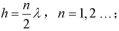

高衍射级的衍射效率增强的条件为:The conditions for enhanced diffraction efficiency of high diffraction orders are:
当衍射光栅的占空比为50%时,槽深h满足
可选地,步骤S3中,栅脊的宽度di的计算公式为:
可选地,衍射效率的计算公式为:Optionally, the calculation formula of diffraction efficiency is:
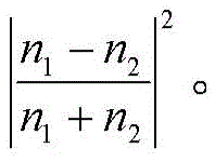
其中,a0为零衍射级的衍射效率,αm为高衍射级的衍射效率,/为占空比,m为衍射级次,h为槽深,n1为入射光在周围介质的折射率,n2为入射光在光栅材料的折射率。Among them, a 0 is the diffraction efficiency of the zero diffraction order, α m is the diffraction efficiency of the high diffraction order, / is the duty cycle, m is the diffraction order, h is the groove depth, and n 1 is the refractive index of the incident light in the surrounding medium , n 2 is the refractive index of the incident light in the grating material.
另一方面,本公开还提供了一种衍射光栅的设计系统,包括:第一获得模块,用于获得衍射光栅衍射光的零衍射级和高衍射级的衍射效率增强和缺级的条件;第二获得模块,用于根据零衍射级缺级的第一条件获得衍射光栅的槽深;第三获得模块,用于根据高衍射级增强的条件获得衍射光栅的栅脊宽度和栅脊之间的距离;复制模块,用于将第三获得模块获得的结构复制并进行对称设置,以使高衍射级的偶衍射级缺级。In another aspect, the present disclosure also provides a diffraction grating design system, comprising: a first obtaining module for obtaining the diffraction efficiency enhancement and order deficiency conditions of the zero diffraction order and high diffraction order of the diffraction grating diffracted light; The second obtaining module is used to obtain the groove depth of the diffraction grating according to the first condition of zero diffraction order and missing orders; the third obtaining module is used to obtain the ridge width of the diffraction grating and the distance between the ridges according to the condition of high diffraction order enhancement. The distance; the replicating module is used for replicating the structure obtained by the third obtaining module and setting it symmetrically, so that the even diffraction order of the high diffraction order is deficient.
可选地,第三获得模块还包括根据零衍射级缺级的第二条件确定栅脊的宽度。Optionally, the third obtaining module further includes determining the width of the grating ridge according to the second condition of zero diffraction order missing order.
可选地,第二条件包括所有栅脊的宽度为光栅周期宽度的一半。Optionally, the second condition includes the width of all ridges being half the width of the grating period.
(三)有益效果(3) Beneficial effects
本公开提供了一种衍射光栅的设计方法及系统,解决了扫描光栅标记过程中计算量大的问题,该方法首先根据各衍射级次增强和缺级的条件,然后根据相位光栅所需增强和缺级的衍射级次,选择满足要求的栅级宽度以及位置信息,获得满足要求的相位光栅结构,该方法根据需要增强的衍射级次,选择相应的栅级和栅槽的宽度和位置,不需要将整个光栅结构均设置为优化条件进行优化,避免了大量计算。The present disclosure provides a method and system for designing a diffraction grating, which solves the problem of a large amount of calculation in the process of scanning the grating marking. The method firstly bases on the conditions of enhancement and lack of each diffraction order, and then according to the required enhancement and loss of the phase grating. For the diffraction order of the missing order, select the grid width and position information that meets the requirements, and obtain the phase grating structure that meets the requirements. The entire grating structure needs to be set to the optimization conditions for optimization, avoiding a lot of computation.
附图说明Description of drawings
图1示意性示出了根据本公开实施例的衍射光栅的设计方法的步骤图;FIG. 1 schematically shows a step diagram of a method for designing a diffraction grating according to an embodiment of the present disclosure;
图2示意性示出了根据本公开实施例的衍射光栅的结构示意图;FIG. 2 schematically shows a schematic structural diagram of a diffraction grating according to an embodiment of the present disclosure;
图3示意性示出了根据本公开实施例的一具体实施例中的衍射光栅的结构示意图;FIG. 3 schematically shows a schematic structural diagram of a diffraction grating in a specific embodiment according to an embodiment of the present disclosure;
图4示意性示出了根据本公开实施例的现有的AH53的结构示意图。FIG. 4 schematically shows a schematic structural diagram of an existing AH53 according to an embodiment of the present disclosure.
具体实施方式Detailed ways
本公提供了一种衍射光栅的设计方法及系统,解决了扫描光栅标记过程中计算量大的问题,该方法首先根据各衍射级次增强和缺级的条件,然后根据相位光栅所需增强和缺级的衍射级次,选择满足要求的栅级宽度以及位置信息,获得满足要求的相位光栅结构,该方法根据需要增强的衍射级次,选择相应的栅级和栅槽的宽度和位置,不需要将整个光栅结构均设置为优化条件进行优化,避免了大量计算。The present disclosure provides a diffraction grating design method and system, which solves the problem of a large amount of calculation in the process of scanning the grating marking. For the diffraction order of the missing order, select the grid width and position information that meets the requirements, and obtain the phase grating structure that meets the requirements. The entire grating structure needs to be set to the optimization conditions for optimization, avoiding a lot of computation.
本公开提供了一种衍射光栅的设计方法,如图1所示,包括:S1,获得衍射光栅衍射光的零衍射级和高衍射级的衍射效率增强和缺级的条件;S2,根据零衍射级缺级的第一条件获得衍射光栅的槽深;S3,根据高衍射级增强的条件获得衍射光栅的栅脊宽度和栅脊之间的距离;S4,将步骤S3获得的结构复制并进行对称设置,以使高衍射级的偶衍射级缺级。The present disclosure provides a method for designing a diffraction grating, as shown in FIG. 1 , including: S1 , obtaining the conditions of diffraction efficiency enhancement and order deficiency of zero diffraction order and high diffraction order of diffraction grating diffracted light; S2 , according to zero diffraction The groove depth of the diffraction grating is obtained under the first condition of order-deficient order; S3, the ridge width of the diffraction grating and the distance between the ridges are obtained according to the condition of high diffraction order enhancement; S4, the structure obtained in step S3 is copied and symmetrical Set so that even diffraction orders of high diffraction orders are missing orders.
为使本发明的目的、技术方案和优点更加清楚明白,以下结合具体实施例,并参照附图,对本发明进一步详细说明。In order to make the objectives, technical solutions and advantages of the present invention clearer, the present invention will be further described in detail below with reference to specific embodiments and accompanying drawings.
S1,获得衍射光栅衍射光的零衍射级和高衍射级的衍射效率增强和缺级的条件,其中,零衍射级缺级的条件包括第一条件和第二条件;S1, obtain the conditions of diffraction efficiency enhancement and order deficiency of the zero diffraction order and high diffraction order of the diffraction grating diffracted light, wherein, the conditions of the zero diffraction order and order deficiency include a first condition and a second condition;
在基于衍射光栅标记的位置测量传感器中,通常只需要衍射光的奇衍射级次增强,偶衍射级次缺级,并且为了提高精度,需增强高衍射级次。因此确定增强高衍射级次,并且使零衍射级和高衍射级次中的偶衍射级缺级的条件。In a position measurement sensor based on diffraction grating markings, only the odd diffraction orders of diffracted light are usually enhanced, the even diffraction orders are missing, and in order to improve accuracy, high diffraction orders need to be enhanced. Therefore, a condition is determined to enhance the high diffraction order, and to make the even diffraction order absent from the zero diffraction order and the high diffraction order.
在设计衍射光栅时,需要确定该衍射光栅的特征参数,如图2所示,如占空比f、槽深h、周期d、材料反射率R等。本公开实施例中以矩形衍射光栅的设计为例对本公开中的方法进行详细介绍。When designing a diffraction grating, it is necessary to determine the characteristic parameters of the diffraction grating, as shown in FIG. 2 , such as duty cycle f, groove depth h, period d, material reflectivity R and so on. In the embodiment of the present disclosure, the method in the present disclosure is described in detail by taking the design of a rectangular diffraction grating as an example.
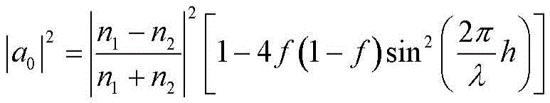
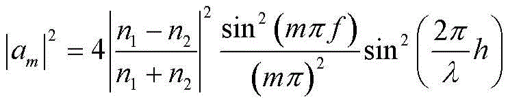
通过分析计算可以得到衍射光栅各衍射级次的衍射效率为:Through analysis and calculation, the diffraction efficiency of each diffraction order of the diffraction grating can be obtained as:


其中,n1为入射光在周围介质的折射率,n2为入射光在光栅材料的折射率,a0为零衍射级的衍射效率,am为第m衍射级的衍射效率。Among them, n 1 is the refractive index of the incident light in the surrounding medium, n 2 is the refractive index of the incident light in the grating material, a 0 is the diffraction efficiency of zero diffraction order, and am is the diffraction efficiency of the mth diffraction order.
根据计算分析,零衍射级的衍射效率增强和缺级的条件为:According to the calculation and analysis, the conditions of the diffraction efficiency enhancement and the missing order of the zero diffraction order are:
当占空比为50%时,槽深满足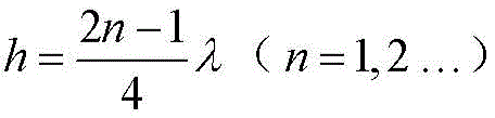
当占空比为50%时,槽深满足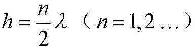
除零衍射级外的其他高衍射级衍射效率增强和缺级的条件为:In addition to the zero diffraction order, the conditions for the enhancement and lack of diffraction efficiency of other high diffraction orders are:
当槽深满足
当槽深满足
当占空比和衍射级乘积满足mf=K(K=1,2...)时,该衍射级的衍射效率增强;When the duty ratio and the diffraction order product satisfy mf=K (K=1, 2...), the diffraction efficiency of the diffraction order is enhanced;
当占空比和衍射级乘积满足
在衍射光栅设计过程中,通常需要保证奇衍射级,尤其是其中的高衍射级衍射效率增强,偶衍射级缺级。通过调整光栅的占空比和槽深可以实现衍射级次的增强和缺级,但是槽深对各衍射级次增强和缺级是以零级光和高级光来区分,不能将偶衍射级和奇衍射级区分,而占空比不仅可以区分偶衍射级次和奇衍射级次,并且可以区分奇衍射级次中的大小。因此衍射光栅的设计可以首先确定槽深。In the design process of the diffraction grating, it is usually necessary to ensure the odd diffraction order, especially the high diffraction order in which the diffraction efficiency is enhanced, and the even diffraction order is missing. By adjusting the duty ratio and groove depth of the grating, the enhancement and missing orders of diffraction orders can be realized, but the enhancement and missing orders of each diffraction order by the groove depth are distinguished by zero-order light and high-order light. Odd diffraction orders are distinguished, and the duty cycle can not only distinguish between even diffraction orders and odd diffraction orders, but also can distinguish the size of odd diffraction orders. Therefore, the design of the diffraction grating can first determine the groove depth.
S2,根据零衍射级缺级的第一条件获得衍射光栅的槽深;S2, obtain the groove depth of the diffraction grating according to the first condition of zero diffraction order and missing order;
由上可知,在槽深为
S3,根据高衍射级增强的条件获得衍射光栅的栅脊宽度和栅脊之间的距离;S3, obtaining the ridge width of the diffraction grating and the distance between the ridges according to the condition of high diffraction order enhancement;
具体的,根据需增强的衍射级次m,引入不同宽度di的栅脊,宽度满足


但为保证零衍射级缺级需满足零衍射级缺级的第二条件,即满足However, in order to ensure the zero-diffraction-order missing order, the second condition of the zero-diffraction-order missing-order must be satisfied, namely

S4,将步骤S3获得的结构复制并进行对称设置,以使高衍射级的偶衍射级缺级。S4, the structure obtained in step S3 is copied and set symmetrically, so that the even diffraction order of the high diffraction order is absent.
例如可以对步骤S3得到的结构整体180°旋转对称,且在半个周期内栅级和栅级之间的栅槽的位置同样满足180°旋转对称,使偶衍射级缺级。For example, the structure obtained in step S3 may be 180° rotationally symmetrical as a whole, and the positions of the grids and the grid grooves between the grids also satisfy 180° rotational symmetry within a half cycle, so that even diffraction orders are missing.
另一方面,本公开还提供了一种衍射光栅的设计系统,包括:In another aspect, the present disclosure also provides a diffraction grating design system, including:
第一获得模块例如可以执行如图1所示的步骤S1,用于获得衍射光栅衍射光的零衍射级和高衍射级的衍射效率增强和缺级的条件;The first obtaining module, for example, can perform step S1 as shown in FIG. 1 , for obtaining the conditions of diffraction efficiency enhancement and order deficiency of the zero diffraction order and high diffraction order of the diffraction grating diffracted light;
第二获得模块例如可以执行如图1所示的步骤S2,用于根据零衍射级缺级的第一条件获得所述衍射光栅的槽深;For example, the second obtaining module may perform step S2 as shown in FIG. 1 , for obtaining the groove depth of the diffraction grating according to the first condition of zero diffraction order and missing orders;
第三获得模块例如可以执行如图1所示的步骤S3,用于根据高衍射级增强的条件获得所述衍射光栅的栅脊宽度和栅脊之间的距离;The third obtaining module may, for example, perform step S3 as shown in FIG. 1 , for obtaining the ridge width and the distance between the ridges of the diffraction grating according to the condition of high diffraction order enhancement;
复制模块例如可以执行如图1所示的步骤S4,用于将第三获得模块获得的结构复制并进行对称设置,以使高衍射级的偶衍射级缺级。For example, the copying module may perform step S4 as shown in FIG. 1 , for copying and symmetrically setting the structure obtained by the third obtaining module, so that even diffraction orders with high diffraction orders are missing orders.
其中,第三获得模块还包括根据零衍射级缺级的第二条件确定栅脊的宽度。第二条件包括所有栅脊的宽度为光栅周期宽度的一半。Wherein, the third obtaining module further includes determining the width of the grating ridge according to the second condition of zero diffraction order missing order. The second condition includes the width of all ridges being half the width of the grating period.
基于上述设计,针对周期为16μm,第5衍射级的衍射效率增强的要求,根据上述步骤可以获得如下图3所示的结构。可以通过严格耦合波电磁仿真的方法,对该结构的效果进行验证。Based on the above design, for the requirement that the period is 16 μm and the diffraction efficiency of the fifth diffraction order is enhanced, the structure shown in Figure 3 below can be obtained according to the above steps. The effect of the structure can be verified by rigorous coupled-wave electromagnetic simulation.
与现有的细分结构AH53(如图4所示)的衍射效率进行比较,该结构和AH53的衍射效率对比如下表1所示,从表1可以看出,该结构不仅第5衍射级衍射效率与原有的细分光栅结构AH53基本相等,同时所有的偶衍射级和零衍射级均缺级,并且第3、7衍射级次的衍射效率比AH53增强,具有较好的性能。Compared with the diffraction efficiency of the existing subdivision structure AH53 (as shown in Figure 4), the comparison of the diffraction efficiency of this structure and AH53 is shown in Table 1 below. It can be seen from Table 1 that this structure not only diffracts the fifth diffraction order. The efficiency is basically the same as the original subdivision grating structure AH53, and all even diffraction orders and zero diffraction orders are missing orders, and the diffraction efficiency of the 3rd and 7th diffraction orders is stronger than that of AH53, which has better performance.
表1Table 1
综上所述,本公开的衍射光栅的设计方法和系统,通过对槽深、栅脊宽度和栅槽宽度进行合理设置,不需将整个光栅结构均设置为优化条件进行优化,避免了大量计算。To sum up, the design method and system of the diffraction grating of the present disclosure, by reasonably setting the groove depth, the width of the gate ridge and the width of the gate groove, do not need to set the entire grating structure as the optimization conditions for optimization, and avoid a lot of calculation. .
以上所述的具体实施例,对本发明的目的、技术方案和有益效果进行了进一步详细说明,所应理解的是,以上所述仅为本发明的具体实施例而已,并不用于限制本发明,凡在本发明的精神和原则之内,所做的任何修改、等同替换、改进等,均应包含在本发明的保护范围之内。The specific embodiments described above further describe the purpose, technical solutions and beneficial effects of the present invention in further detail. It should be understood that the above descriptions are only specific embodiments of the present invention, and are not intended to limit the present invention. Any modification, equivalent replacement, improvement, etc. made within the spirit and principle of the present invention shall be included within the protection scope of the present invention.
Claims (10)


Priority Applications (1)
| Application Number | Priority Date | Filing Date | Title |
|---|---|---|---|
| CN202010594125.7A CN111610586B (en) | 2020-06-24 | 2020-06-24 | Design method and system for a diffraction grating |
Applications Claiming Priority (1)
| Application Number | Priority Date | Filing Date | Title |
|---|---|---|---|
| CN202010594125.7A CN111610586B (en) | 2020-06-24 | 2020-06-24 | Design method and system for a diffraction grating |
Publications (2)
| Publication Number | Publication Date |
|---|---|
| CN111610586A true CN111610586A (en) | 2020-09-01 |
| CN111610586B CN111610586B (en) | 2022-04-29 |
Family
ID=72195553
Family Applications (1)
| Application Number | Title | Priority Date | Filing Date |
|---|---|---|---|
| CN202010594125.7A Active CN111610586B (en) | 2020-06-24 | 2020-06-24 | Design method and system for a diffraction grating |
Country Status (1)
| Country | Link |
|---|---|
| CN (1) | CN111610586B (en) |
Cited By (3)
| Publication number | Priority date | Publication date | Assignee | Title |
|---|---|---|---|---|
| CN112833790A (en) * | 2021-01-21 | 2021-05-25 | 中国科学院微电子研究所 | A method to reduce the influence of phase grating asymmetry on position measurement accuracy |
| CN112902996A (en) * | 2021-01-21 | 2021-06-04 | 中国科学院微电子研究所 | Phase grating structure with enhanced diffraction efficiency of 9 th diffraction order |
| CN116222422A (en) * | 2023-01-17 | 2023-06-06 | 中国科学院微电子研究所 | A phase grating position measurement system and method for measuring structural parameters |
Citations (7)
| Publication number | Priority date | Publication date | Assignee | Title |
|---|---|---|---|---|
| CN1936710A (en) * | 2006-10-18 | 2007-03-28 | 上海微电子装备有限公司 | Alignment mark and its producing method |
| CN101504925A (en) * | 2009-03-06 | 2009-08-12 | 上海微电子装备有限公司 | Optical position measurement apparatus and method |
| US20100277797A1 (en) * | 2009-05-01 | 2010-11-04 | Toyota Motor Engineering And Manufacturing North America, Inc. | Grating structure for splitting light |
| CN108204828A (en) * | 2016-12-20 | 2018-06-26 | 约翰内斯·海德汉博士有限公司 | Optical location device |
| CN108369087A (en) * | 2015-12-08 | 2018-08-03 | 科磊股份有限公司 | Using polarization target and polarization illumination to control the amplitude and phase of the order of diffraction |
| CN109154718A (en) * | 2016-04-29 | 2019-01-04 | 微软技术许可有限责任公司 | Robust Architecture for Large Field of View Components |
| CN110875342A (en) * | 2018-09-03 | 2020-03-10 | 三星电子株式会社 | Image sensor having grating structure therein providing enhanced diffraction of incident light |
-
2020
- 2020-06-24 CN CN202010594125.7A patent/CN111610586B/en active Active
Patent Citations (7)
| Publication number | Priority date | Publication date | Assignee | Title |
|---|---|---|---|---|
| CN1936710A (en) * | 2006-10-18 | 2007-03-28 | 上海微电子装备有限公司 | Alignment mark and its producing method |
| CN101504925A (en) * | 2009-03-06 | 2009-08-12 | 上海微电子装备有限公司 | Optical position measurement apparatus and method |
| US20100277797A1 (en) * | 2009-05-01 | 2010-11-04 | Toyota Motor Engineering And Manufacturing North America, Inc. | Grating structure for splitting light |
| CN108369087A (en) * | 2015-12-08 | 2018-08-03 | 科磊股份有限公司 | Using polarization target and polarization illumination to control the amplitude and phase of the order of diffraction |
| CN109154718A (en) * | 2016-04-29 | 2019-01-04 | 微软技术许可有限责任公司 | Robust Architecture for Large Field of View Components |
| CN108204828A (en) * | 2016-12-20 | 2018-06-26 | 约翰内斯·海德汉博士有限公司 | Optical location device |
| CN110875342A (en) * | 2018-09-03 | 2020-03-10 | 三星电子株式会社 | Image sensor having grating structure therein providing enhanced diffraction of incident light |
Cited By (4)
| Publication number | Priority date | Publication date | Assignee | Title |
|---|---|---|---|---|
| CN112833790A (en) * | 2021-01-21 | 2021-05-25 | 中国科学院微电子研究所 | A method to reduce the influence of phase grating asymmetry on position measurement accuracy |
| CN112902996A (en) * | 2021-01-21 | 2021-06-04 | 中国科学院微电子研究所 | Phase grating structure with enhanced diffraction efficiency of 9 th diffraction order |
| CN112833790B (en) * | 2021-01-21 | 2023-03-14 | 中国科学院微电子研究所 | A Method for Reducing the Influence of Phase Grating Asymmetry on Position Measurement Accuracy |
| CN116222422A (en) * | 2023-01-17 | 2023-06-06 | 中国科学院微电子研究所 | A phase grating position measurement system and method for measuring structural parameters |
Also Published As
| Publication number | Publication date |
|---|---|
| CN111610586B (en) | 2022-04-29 |
Similar Documents
| Publication | Publication Date | Title |
|---|---|---|
| US11675277B2 (en) | Self-referencing and self-calibrating interference pattern overlay measurement | |
| CN111610586A (en) | Design method and system for a diffraction grating | |
| KR102202517B1 (en) | Metrology using overlay and yield critical patterns | |
| JP6770958B2 (en) | Landscape analysis and utilization | |
| US11060845B2 (en) | Polarization measurements of metrology targets and corresponding target designs | |
| CN112331576B (en) | Metering target design method and verification metering target | |
| KR102467186B1 (en) | Test structures and metrology technique utilizing the test structures for measuring in patterned structures | |
| TW201606444A (en) | Focus measurement using scatterometry | |
| TWI401549B (en) | Method for designing two dimensional overlay array target and method and system for measureing overlay error using the same | |
| US20090220872A1 (en) | Detecting apparatus, exposure apparatus, and device manufacturing method | |
| WO2021072792A1 (en) | Machine learning-based method for determining focal plane position of photolithography system | |
| US7858271B2 (en) | Method of measuring dimension of pattern and method of forming pattern | |
| Leray et al. | Improving scanner wafer alignment performance by target optimization | |
| Fuchimoto et al. | Measurement technology to quantify 2D pattern shape in sub-2x nm advanced lithography | |
| CN103454861B (en) | The mark that a kind of alignment is measured and method | |
| CN101452202A (en) | PSM, exposure focus calibrating method by utilizing PSM and system thereof | |
| Ausschnitt et al. | Pattern shift response metrology | |
| CN112902996B (en) | Phase grating structure with enhanced diffraction efficiency of 9 th diffraction order | |
| CN111580206A (en) | A kind of diffraction grating structure and preparation method thereof | |
| CN119554948A (en) | Method, device and system for correcting measurement errors caused by asymmetric overlay marks | |
| US10311198B2 (en) | Overlay design optimization | |
| CN204287729U (en) | A kind of test structure for monitoring exposure defocusing | |
| KR20240059563A (en) | Phase difference measuring apparatus and phase difference measuring method | |
| US20160018819A1 (en) | Identifying registration errors of dsa lines | |
| CN121209221A (en) | Overlay mark and overlay error measurement method thereof |
Legal Events
| Date | Code | Title | Description |
|---|---|---|---|
| PB01 | Publication | ||
| PB01 | Publication | ||
| SE01 | Entry into force of request for substantive examination | ||
| SE01 | Entry into force of request for substantive examination | ||
| GR01 | Patent grant | ||
| GR01 | Patent grant |