Disclosure of Invention
One aspect of the present application provides a semiconductor packaging method, including:
forming a carrier plate with a first metal connecting piece, wherein the first metal connecting piece extends inwards from the upper surface of the carrier plate;
arranging a chip on the carrier plate; the first metal connecting piece is connected with a functional end of the lower surface of the chip;
packaging the chip on the carrier plate to form a first packaging layer;
disposing a second metal connector through the first encapsulant layer over the chip; and the second metal connecting piece is connected with the functional end of the upper surface of the chip.
Optionally, the second metal connector includes a first connection portion, and the second metal connector disposed on the chip and penetrating through the first encapsulation layer includes:
a second connecting piece opening corresponding to the functional end of the upper surface of the chip is formed in the first packaging layer;
a first connector portion is disposed in the second connector aperture.
Optionally, the second metal connecting piece includes a second connecting portion connected to the first connecting portion, and after the first connecting portion is disposed in the second connecting piece opening, the method includes:
disposing a second connection portion over the first connection portion; wherein the cross-sectional dimension of the second connecting portion is greater than the cross-sectional dimension of the first connecting portion.
Optionally, the carrier plate includes a first carrier plate layer and a second carrier plate layer; the forming a carrier plate with a first metal connecting piece comprises:
forming a first carrier layer over a substrate;
arranging a first metal connecting piece on one side of the first carrier plate layer, which is far away from the substrate;
carrying out plastic package on the first metal connecting piece to form a second carrier plate layer;
and removing the substrate.
Optionally, the disposing a first metal connecting element on a side of the first carrier layer away from the substrate includes:
forming a first metal layer on one side of the first carrier plate layer far away from the substrate;
forming a second metal layer over the first metal layer;
and removing at least part of the first metal layer and the second metal layer to form a first metal connecting piece.
Optionally, the disposing a first metal connector on a side of the first carrier layer away from the substrate includes:
forming a first metal layer on one side of the first carrier plate layer far away from the substrate;
forming a second metal layer over the first metal layer;
forming a third metal layer on the second metal layer at intervals;
and removing the first metal layer and the second metal layer corresponding to the interval of the third metal layer to form the first metal connecting piece.
Optionally, after removing the substrate, the method includes:
and thinning the second carrier plate layer to expose the first metal connecting piece.
Optionally, the forming the carrier board with the first metal connecting piece includes:
forming a carrier plate on the substrate;
arranging a first metal connecting piece extending inwards from the upper surface of the carrier plate on one side of the carrier plate away from the substrate;
and removing the substrate.
Optionally, the first metal connecting piece arranged on one side of the carrier plate away from the substrate and extending inwards from the upper surface of the carrier plate away from the substrate includes:
opening a first connecting piece opening on one side of the carrier plate, which is far away from the substrate;
a first metal connecting piece is arranged in the first connecting piece opening.
Optionally, after disposing a second metal connector through the first encapsulation layer over the chip, the method includes:
plastically packaging the second metal connecting piece on the first packaging layer to form a second packaging layer;
and thinning the carrier plate layer and the second packaging layer, and exposing the lower surface of the first metal connecting piece and the upper surface of the second metal connecting piece.
Another aspect of the present application provides a semiconductor package structure, including:
a carrier plate having a first metal connector extending inwardly from an upper surface of the carrier plate;
the chip is arranged on the carrier plate; the first metal connecting piece is connected with a functional end of the lower surface of the chip;
the first encapsulating layer is arranged on the carrier plate and encapsulates the chip;
and the second metal connecting piece penetrates through the first encapsulating layer and is connected with the functional end of the upper surface of the chip.
In the semiconductor package method and the semiconductor package structure provided by this embodiment, the first metal connecting member is formed on the carrier, so that the first metal connecting member is directly connected to the functional end of the lower surface of the chip when the chip is disposed on the carrier, and the second metal connecting member connected to the functional end of the upper surface of the chip is disposed in the first encapsulation layer after the first encapsulation layer is formed by plastic encapsulation on the upper surface of the chip. Therefore, the formed semiconductor product is not easy to be influenced by the metal connecting piece because no plastic packaging material overflows after plastic packaging, the connection stability of the metal connecting piece is ensured, and the packaging yield of the semiconductor product is improved.
Detailed Description
Reference will now be made in detail to the exemplary embodiments, examples of which are illustrated in the accompanying drawings. When the following description refers to the accompanying drawings, like numbers in different drawings represent the same or similar elements unless otherwise indicated. The embodiments described in the following exemplary embodiments do not represent all embodiments consistent with the present application. Rather, they are merely examples of apparatus and methods consistent with certain aspects of the present application, as detailed in the appended claims.
The terminology used herein is for the purpose of describing particular embodiments only and is not intended to be limiting of the application. Unless defined otherwise, technical or scientific terms used herein shall have the ordinary meaning as understood by one of ordinary skill in the art to which this invention belongs. The use of the terms "a" or "an" and the like in the description and in the claims of this application do not denote a limitation of quantity, but rather denote the presence of at least one. "plurality" means two or more. The word "comprising" or "comprises", and the like, means that the element or item listed as preceding "comprising" or "includes" covers the element or item listed as following "comprising" or "includes" and its equivalents, and does not exclude other elements or items. The terms "connected" or "coupled" and the like are not restricted to physical or mechanical connections, but may include electrical connections, whether direct or indirect. "Upper" and/or "lower," and the like, are used for convenience of description and are not limited to a single position or orientation in space. As used in this specification and the appended claims, the singular forms "a", "an", and "the" are intended to include the plural forms as well, unless the context clearly indicates otherwise. It should also be understood that the term "and/or" as used herein refers to and encompasses any and all possible combinations of one or more of the associated listed items.
In the semiconductor packaging technology, two-sided interconnection of a plurality of chips is generally realized by using aluminum wires, copper strips, or a plurality of welding wires through processes of welding, bonding and the like, or by using leadless packaging and through in-hole metallization. However, the two sides of the chip are interconnected by using aluminum wires, copper strips, or a plurality of welding wires, and the electrical performance of the packaged product is poor. However, the leadless package is adopted, and the interconnection is realized through the metallization in the hole, which is generally limited by the factors such as the depth and the diameter of the laser drilling, and the manufacturing process is complex.
In order to solve the above-mentioned problems in the semiconductor packaging technology, the present application provides a semiconductor packaging method. In the packaging process, first, a carrier board having a first metal connecting member is formed, wherein the first metal connecting member extends inward from an upper surface of the carrier board. Further, a chip is arranged on the carrier plate; the first metal connecting piece is connected with the functional end of the lower surface of the chip. And then, packaging the chip on the carrier plate to form a first packaging layer. Finally, a second metal connecting piece penetrating through the first packaging layer is arranged above the chip; and the second metal connecting piece is connected with the functional end of the upper surface of the chip. In the above embodiment of the present disclosure, the first metal connecting part is formed on the carrier plate, so that the first metal connecting part is directly connected to the functional end of the lower surface of the chip when the chip is disposed on the carrier plate, and after the first encapsulation layer is formed by plastic encapsulation on the upper surface of the chip, the second metal connecting part connected to the functional end of the upper surface of the chip is disposed in the first encapsulation layer. Therefore, the two sides of the formed semiconductor product can be electrically connected with other structural parts, and the semiconductor product is not overflowed by plastic package materials after plastic package, so that the semiconductor structure is not easily influenced by metal connecting pieces, and the stability of connection of the metal connecting pieces is favorably ensured.
Referring to fig. 1, 2(a) -2 (l) and 3(a) -3 (j), the present disclosure provides a semiconductor packaging method and a semiconductor packaging structure.
Fig. 1 is a flowchart of a proposed semiconductor packaging method according to an exemplary embodiment of the present disclosure. As shown in fig. 1, the semiconductor packaging method includes the following steps 101 to 104:
in step 101, a carrier board having a first metal connecting element is formed, wherein the first metal connecting element extends inward from an upper surface of the carrier board.
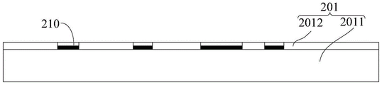
As shown in fig. 2(a) -2 (l), an embodiment of a carrier board 201 having a first metal connecting member 210 is provided. As shown in fig. 2(a) and 2(b), an adhesive layer 102 is provided on a substrate 101 to form a carrier 201 on the substrate 101, and the carrier 201 is provided on the substrate 101 through the adhesive layer 102 and can be more firmly adhered to the substrate 101. Thereby facilitating subsequent operations such as disposing the first metal connecting element 210 on the carrier 201.
The adhesive layer 102 may be made of a material that is easily peelable to peel off the substrate 101 and the carrier board 201 having the first metal connecting members 210, for example, a thermal release material that can be removed from its adhesiveness by heating. The adhesive layer 102 may be specifically a thermal decomposition film formed by coating a thermal separation material on the substrate 101.
As shown in fig. 2(c), a first carrier layer 2011 is disposed on the adhesive layer. The first carrier plate layer may be formed by Compression molding.
As shown in fig. 2(d), after the first carrier layer 2011 is formed, a first metal layer (not shown) is formed on a side of the first carrier layer away from the substrate 101. The first metal layer may be formed by sputtering. The first metal layer may further include two metal material layers. For example, the first metal layer may include a metal titanium (Ti) layer and a metal copper (Cu) layer. Alternatively, the first metal layer may comprise a 0.2um metallic titanium layer and a 0.2-0.5 um metallic copper layer. Of course, the first metal layer may also comprise only one layer of metal material, such as only one layer of metal titanium.
After the first metal layer is formed, a second metal layer 211 is formed over the first metal layer. The second metal layer 211 may be formed by electroplating. The material of the second metal layer 211 may include metallic copper or an alloy including metallic copper. Optionally, the thickness of the second metal layer is in the range of 0.8-1.2 μm, such as 1 μm.
As shown in fig. 2(e), 2(f) and 2(g), a photosensitive film layer 203 is attached on the second metal layer 211 (fig. 2 (e)), and a plurality of openings 204 are formed in the photosensitive film layer 203 by exposure (fig. 2 (f)) and development (fig. 2 (g)). The location of this opening 204 may be set according to the specific needs of the desired first metal connection.
As shown in fig. 2(h), a third metal layer 212 is disposed in the plurality of openings 204. The material of the third metal layer 212 may include metallic copper or an alloy including metallic copper.
As shown in fig. 2(i), the photosensitive film layers 203 on both sides of the third metal layer 212 are cleaned and removed, and the first metal layer and the second metal layer corresponding to the space between the third metal layer 212 are removed, and the first metal layer and the second metal layer right below the third metal layer 212 remain, so as to form the first metal connection element 210 including a portion of the first metal layer, a portion of the second metal layer 211, and the third metal layer 212. The first metal connecting member 210 has a flat plate shape.
As shown in fig. 2(j), the first metal connecting member 210 is molded on the first carrier layer 2011 to form a second carrier layer 2012. Thereby forming a carrier 201 having a first carrier layer 2011 and a second carrier layer 2012. The material of the second carrier layer 2012 can be the same as the material of the first carrier layer 2011. In some alternative embodiments, the first carrier layer 2011 and the second carrier layer 2012 may be integrated.
As shown in fig. 2(k), the substrate 101 is removed from below the carrier 201. When the adhesive layer 102 between the substrate 101 and the carrier 201 has a thermal release material, the thermal release material on the adhesive layer 102 may be heated to reduce its viscosity after being heated, so as to peel off the substrate 101. In other embodiments, the substrate 101 may be mechanically peeled directly.
As shown in fig. 2(l), the carrier board 201 is thinned. Specifically, the upper surface of the second carrier layer 2012 is thinned to expose the upper surface of the first metal connecting element 210. In specific implementation, the carrier plate 201 may be thinned by grinding. After the carrier board 201 is thinned, the upper surface of the carrier board and the upper surface of the first metal connecting element 210 may be in the same plane, or substantially in the same plane, so as to facilitate subsequent operations of mounting a chip and the like.
Of course, in some other embodiments, the upper surface of the second carrier layer 2012 is disposed in the same plane or substantially the same plane as the upper surface of the first metal connecting element when being molded, so that the upper surface of the first metal connecting element 210 is exposed, and the second carrier layer 2012 may not be thinned. The present application is not limited to this, and may be set according to a specific application environment.
When the thickness of the second metal layer 211 and the like satisfy the electrical connection performance, the third metal layer may not be provided. Accordingly, after the second metal layer 211 is formed, at least a portion of the first metal layer and at least a portion of the second metal layer 211 are removed, and the first metal connection 210 is formed.
It should be further noted that, in some other embodiments, step 101 can also be implemented by the following steps 1011, 1012 and 1013:
in step 1011, a carrier is formed over the substrate. The formation of the carrier can refer to the related description above, and will not be described herein.
In step 1012, a first metal connector extending inward from the upper surface of the carrier away from the substrate is disposed on the side of the carrier away from the substrate.
In an optional implementation, a first connecting member opening may be formed in a side of the carrier board away from the substrate, and a first metal connecting member is disposed in the first connecting member opening. In some embodiments, the first connector opening may be formed by laser opening. In other embodiments, the first connecting member opening may be formed by photolithography patterning, i.e., the first connecting member opening may be formed by attaching a photosensitive film, exposing, and developing. Correspondingly, the first metal connecting piece is arranged in the first connecting piece opening hole and can be realized by adopting sputtering, electroplating and the like. The material of the first metal connecting member can refer to the related description above, and the application does not limit this.
In step 1013, the substrate is removed. Reference is made to the above description, which is not repeated herein.
In step 102, a chip is disposed on a carrier; the first metal connecting piece is connected with the functional end of the lower surface of the chip.
In some embodiments, the number of the first metal connecting pieces is multiple. Of course, in other embodiments, the number of the first metal connecting pieces may be one. The present application is not limited to this, and may be set according to a specific application environment.
As shown in fig. 3(a), a chip 202 is disposed on a carrier 201 having a plurality of first metal connectors 210. The lower surface of the chip 202 is connected to the plurality of first metal connectors 210, and the plurality of first metal connectors 210 can be electrically connected to the functional terminals on the lower surface of the chip 202.
In some embodiments, the first metal connecting member 210 is shaped like a flat plate, so that when the chip 202 is disposed on the carrier 201, the chip disposed on the carrier 201 is stable and not easy to tilt, which is convenient for disposing the chip 202 on the carrier and is beneficial for the subsequent operations.
In step 103, the chip is packaged on the carrier to form a first encapsulation layer. The first encapsulant layer is capable of encapsulating at least a portion of the chip.
As shown in fig. 3(b), a first encapsulating layer 205 capable of completely encapsulating the chip 202 is formed over the carrier 201. The first encapsulation layer 205 may be formed by laminating an epoxy resin film or abf (ajinomoto build film), or may be formed by Injection molding (Injection molding), Compression molding (Compression molding), or Transfer molding (Transfer molding) of an epoxy resin compound.
In step 104, a second metal connector is arranged on the chip and penetrates through the first packaging layer; and the second metal connecting piece is connected with the functional end of the upper surface of the chip.
In some embodiments, the number of the second metal connectors is plural. Of course, in other embodiments, the number of the second metal connecting pieces may be one.
As shown in fig. 3(c) -3 (i), an embodiment is provided in which a plurality of second metal connectors 220 are provided. It should be noted that, the method may also be adopted when one second metal connecting element 220 is arranged, and the method is not limited in this application and may be arranged according to a specific application environment.
As shown in fig. 3(c), a second connector opening 206 is opened in the first encapsulant layer 205. The second connector opening 206 is disposed on the chip 202 and corresponds to a functional end of the upper surface of the chip 202. The second connector opening 206 may be laser drilled.
As shown in fig. 3(d), a fourth metal layer 207 may be disposed on the second connector opening 206 and the upper surface of the first encapsulation layer 205. The arrangement and material of the fourth metal layer are substantially the same as those of the first metal layer, and reference may be made to the description of the first metal layer, which is not repeated herein.
As shown in fig. 3(e) and 3(f), a photosensitive film layer 208 is disposed on the fourth metal layer 207, and an opening 209 is opened by exposure and development. Wherein the opening 209 is opened above the second connector opening 206. And the cross-sectional dimension of the opening 209 is greater than the cross-sectional dimension of the second connector opening 206. It will also be appreciated that the aperture of the opening 209 is larger than the aperture of the second connector opening 206.
Of course, in some other embodiments without the fourth metal layer, the photosensitive film layer 208 may be directly disposed on the second connection member opening 206 and the first encapsulation layer 205, and the opening 209 may be formed.
As shown in fig. 3(g), a second metal connection 220 is disposed in the second connection opening 206 and the opening 209. The second metal connector 220 includes a first connecting portion 2201 disposed in the second connector opening 206 and a second connecting portion 2202 disposed in the opening 209. Corresponding to the second connector holes 206 and 209, the cross-sectional dimension of the second connecting portion 2202 is larger than that of the first connecting portion 2201, so as to increase the dimension of the upper surface of the second metal connector 220 and ensure electrical connection with other structural members or other products. Of course, in other embodiments, the second metal connector 220 may also include only the first connector 2201. In the case where the upper surface of the first connection portion 2201 is large, which can ensure electrical connection with other structural members or other products, the second connection portion 2202 may not be provided. Accordingly, after the second connector opening 206 is opened, the first connection portion 2201 may be directly disposed in the second connector opening 206 or disposed after the fourth metal layer 207 is formed.
In some embodiments, the second metal connecting element 220 may be disposed by electroplating. Alternatively, the material of the second metal connecting member 220 may include metallic copper or an alloy including metallic copper.
Further, after the second metal connectors 220 are disposed, the photosensitive film layer 208 and metal debris are removed by cleaning, so as to expose the upper portions of the second metal connectors 220 and the first encapsulation layer 205 between the plurality of second metal connectors 220.
As shown in fig. 3(h), the second metal connector 220 is molded on the exposed first encapsulant layer 205 to form a second encapsulant layer 214. The second encapsulant layer 214 may be formed by laminating an epoxy resin film or abf (ajinomoto build film), or may be formed by Injection molding (Injection molding), Compression molding (Compression molding), or Transfer molding (Transfer molding) of an epoxy resin compound.
As shown in fig. 3(i), the carrier 201 and the second encapsulant layer 214 are thinned, the lower surface of the carrier 201 may be thinned to be flush with the lower surface of the first metal connecting element 210 to expose the lower surface of the first metal connecting element, and the upper surface of the second encapsulant layer 214 may be thinned to be flush with the upper surface of the second metal connecting element 220 to expose the upper surface of the second metal connecting element 220. In some embodiments, the carrier 201 and the second encapsulant 214 may be thinned by grinding.
Further, after step 104, a metal connection layer may be disposed on the exposed lower surface of the first metal connecting element 210 by electroplating or ball-planting, so as to ensure or enhance the electrical connection with other products or structures. As shown in fig. 3(j), a metal connection layer 250 is disposed on the exposed lower surface of the first metal connection member 210 by electroplating or ball-planting. Similarly, a metal connection layer may be disposed on the exposed upper surface of the second metal connecting element 220 by electroplating or ball-planting, so as to ensure or enhance electrical connection with other products or structures. As shown in fig. 3(j), a metal connection layer 240 is disposed on the exposed upper surface of the second metal connecting element 220 by electroplating or ball-planting.
In the semiconductor package method and the semiconductor package structure provided by this embodiment, the first metal connecting member is formed on the carrier, so that the first metal connecting member is directly connected to the functional end of the lower surface of the chip when the chip is disposed on the carrier, and the second metal connecting member connected to the functional end of the upper surface of the chip is disposed in the first encapsulation layer after the first encapsulation layer is formed by plastic encapsulation on the upper surface of the chip. Therefore, the two sides of the formed semiconductor product can be electrically connected with other structural parts, and no plastic packaging material overflows after plastic packaging, so that the semiconductor structure is not easily influenced by the metal connecting piece, the connection stability of the metal connecting piece is guaranteed, and the packaging yield of the semiconductor product is improved. In the above embodiment, the first metal connecting part formed by forming the metal layer and the second metal connecting part formed by electroplating or the like are used, so that the thicknesses of the first metal connecting part and the second metal connecting part are greatly reduced compared with the existing metal sheet which needs to be welded and fixed to form the metal contact of the chip, and the thickness of the whole semiconductor product is favorably reduced. In addition, compared with the conventional method of directly welding metal sheets to form metal contacts of the chip, the arrangement of the first metal connecting piece and the second metal connecting piece in the above embodiment is not limited by the size of the metal sheets, so that a plurality of metal connecting pieces can be arranged on both sides of the chip, and the chip can be better electrically connected with other structural members.
The present application further provides a semiconductor package structure, which can also be seen in fig. 3(j), and the semiconductor package structure includes a carrier 201, a chip 202, a first encapsulant layer 205, and a second metal connector 220. The method comprises the following specific steps:
the carrier 201 has a first metal connecting element 210, and the first metal connecting element 210 extends inward from the upper surface of the carrier.
The chip 202 is disposed on the carrier 201. The first metal connecting member 210 is connected to the functional terminal on the lower surface of the chip 202.
The first encapsulation layer 205 is disposed on the carrier 201 and encapsulates the chip 202.
The second metal connector 220 is connected to the functional terminal on the upper surface of the chip 202 through the first encapsulant layer 205.
Further, in some embodiments, the semiconductor package structure further includes a second encapsulant layer 214. The semiconductor package structure includes a plurality of second metal connectors 220. The upper surface of the encapsulation layer 214 is flush with the upper surfaces of the plurality of second metal connectors 220, and can cover all or part of the upper surface of the first encapsulation layer 205 between the plurality of second metal connectors 220.
In the present embodiment, each structural element of the semiconductor package structure can refer to the related description of the corresponding structural element in the semiconductor package method, which is not repeated herein.
In the present application, the apparatus embodiments and the method embodiments may complement each other without conflict.
The above description is only exemplary of the present application and should not be taken as limiting the present application, as any modification, equivalent replacement, or improvement made within the spirit and principle of the present application should be included in the scope of protection of the present application.