CN111580744A - Memory controller and operating method thereof - Google Patents
Memory controller and operating method thereof Download PDFInfo
- Publication number
- CN111580744A CN111580744A CN201911012119.XA CN201911012119A CN111580744A CN 111580744 A CN111580744 A CN 111580744A CN 201911012119 A CN201911012119 A CN 201911012119A CN 111580744 A CN111580744 A CN 111580744A
- Authority
- CN
- China
- Prior art keywords
- map data
- mapping
- memory
- extended
- map
- Prior art date
- Legal status (The legal status is an assumption and is not a legal conclusion. Google has not performed a legal analysis and makes no representation as to the accuracy of the status listed.)
- Granted
Links
Images


Classifications
-
- G—PHYSICS
- G06—COMPUTING OR CALCULATING; COUNTING
- G06F—ELECTRIC DIGITAL DATA PROCESSING
- G06F12/00—Accessing, addressing or allocating within memory systems or architectures
- G06F12/02—Addressing or allocation; Relocation
- G06F12/08—Addressing or allocation; Relocation in hierarchically structured memory systems, e.g. virtual memory systems
- G06F12/10—Address translation
-
- G—PHYSICS
- G06—COMPUTING OR CALCULATING; COUNTING
- G06F—ELECTRIC DIGITAL DATA PROCESSING
- G06F12/00—Accessing, addressing or allocating within memory systems or architectures
- G06F12/02—Addressing or allocation; Relocation
- G06F12/0223—User address space allocation, e.g. contiguous or non contiguous base addressing
- G06F12/023—Free address space management
- G06F12/0238—Memory management in non-volatile memory, e.g. resistive RAM or ferroelectric memory
- G06F12/0246—Memory management in non-volatile memory, e.g. resistive RAM or ferroelectric memory in block erasable memory, e.g. flash memory
-
- G—PHYSICS
- G06—COMPUTING OR CALCULATING; COUNTING
- G06F—ELECTRIC DIGITAL DATA PROCESSING
- G06F11/00—Error detection; Error correction; Monitoring
- G06F11/07—Responding to the occurrence of a fault, e.g. fault tolerance
- G06F11/08—Error detection or correction by redundancy in data representation, e.g. by using checking codes
- G06F11/10—Adding special bits or symbols to the coded information, e.g. parity check, casting out 9's or 11's
- G06F11/1008—Adding special bits or symbols to the coded information, e.g. parity check, casting out 9's or 11's in individual solid state devices
- G06F11/1068—Adding special bits or symbols to the coded information, e.g. parity check, casting out 9's or 11's in individual solid state devices in sector programmable memories, e.g. flash disk
-
- G—PHYSICS
- G06—COMPUTING OR CALCULATING; COUNTING
- G06F—ELECTRIC DIGITAL DATA PROCESSING
- G06F12/00—Accessing, addressing or allocating within memory systems or architectures
- G06F12/02—Addressing or allocation; Relocation
- G06F12/06—Addressing a physical block of locations, e.g. base addressing, module addressing, memory dedication
- G06F12/0638—Combination of memories, e.g. ROM and RAM such as to permit replacement or supplementing of words in one module by words in another module
-
- G—PHYSICS
- G06—COMPUTING OR CALCULATING; COUNTING
- G06F—ELECTRIC DIGITAL DATA PROCESSING
- G06F3/00—Input arrangements for transferring data to be processed into a form capable of being handled by the computer; Output arrangements for transferring data from processing unit to output unit, e.g. interface arrangements
- G06F3/06—Digital input from, or digital output to, record carriers, e.g. RAID, emulated record carriers or networked record carriers
- G06F3/0601—Interfaces specially adapted for storage systems
- G06F3/0628—Interfaces specially adapted for storage systems making use of a particular technique
- G06F3/0638—Organizing or formatting or addressing of data
- G06F3/064—Management of blocks
-
- G—PHYSICS
- G06—COMPUTING OR CALCULATING; COUNTING
- G06F—ELECTRIC DIGITAL DATA PROCESSING
- G06F3/00—Input arrangements for transferring data to be processed into a form capable of being handled by the computer; Output arrangements for transferring data from processing unit to output unit, e.g. interface arrangements
- G06F3/06—Digital input from, or digital output to, record carriers, e.g. RAID, emulated record carriers or networked record carriers
- G06F3/0601—Interfaces specially adapted for storage systems
- G06F3/0628—Interfaces specially adapted for storage systems making use of a particular technique
- G06F3/0638—Organizing or formatting or addressing of data
- G06F3/0644—Management of space entities, e.g. partitions, extents, pools
-
- G—PHYSICS
- G06—COMPUTING OR CALCULATING; COUNTING
- G06F—ELECTRIC DIGITAL DATA PROCESSING
- G06F3/00—Input arrangements for transferring data to be processed into a form capable of being handled by the computer; Output arrangements for transferring data from processing unit to output unit, e.g. interface arrangements
- G06F3/06—Digital input from, or digital output to, record carriers, e.g. RAID, emulated record carriers or networked record carriers
- G06F3/0601—Interfaces specially adapted for storage systems
- G06F3/0628—Interfaces specially adapted for storage systems making use of a particular technique
- G06F3/0655—Vertical data movement, i.e. input-output transfer; data movement between one or more hosts and one or more storage devices
- G06F3/0658—Controller construction arrangements
-
- G—PHYSICS
- G06—COMPUTING OR CALCULATING; COUNTING
- G06F—ELECTRIC DIGITAL DATA PROCESSING
- G06F3/00—Input arrangements for transferring data to be processed into a form capable of being handled by the computer; Output arrangements for transferring data from processing unit to output unit, e.g. interface arrangements
- G06F3/06—Digital input from, or digital output to, record carriers, e.g. RAID, emulated record carriers or networked record carriers
- G06F3/0601—Interfaces specially adapted for storage systems
- G06F3/0668—Interfaces specially adapted for storage systems adopting a particular infrastructure
- G06F3/0671—In-line storage system
- G06F3/0683—Plurality of storage devices
-
- G—PHYSICS
- G06—COMPUTING OR CALCULATING; COUNTING
- G06F—ELECTRIC DIGITAL DATA PROCESSING
- G06F2212/00—Indexing scheme relating to accessing, addressing or allocation within memory systems or architectures
- G06F2212/65—Details of virtual memory and virtual address translation
- G06F2212/657—Virtual address space management
-
- G—PHYSICS
- G06—COMPUTING OR CALCULATING; COUNTING
- G06F—ELECTRIC DIGITAL DATA PROCESSING
- G06F2212/00—Indexing scheme relating to accessing, addressing or allocation within memory systems or architectures
- G06F2212/72—Details relating to flash memory management
- G06F2212/7201—Logical to physical mapping or translation of blocks or pages
-
- G—PHYSICS
- G06—COMPUTING OR CALCULATING; COUNTING
- G06F—ELECTRIC DIGITAL DATA PROCESSING
- G06F2212/00—Indexing scheme relating to accessing, addressing or allocation within memory systems or architectures
- G06F2212/72—Details relating to flash memory management
- G06F2212/7204—Capacity control, e.g. partitioning, end-of-life degradation
Landscapes
- Engineering & Computer Science (AREA)
- Theoretical Computer Science (AREA)
- Physics & Mathematics (AREA)
- General Engineering & Computer Science (AREA)
- General Physics & Mathematics (AREA)
- Human Computer Interaction (AREA)
- Quality & Reliability (AREA)
- Techniques For Improving Reliability Of Storages (AREA)
- Memory System (AREA)
Abstract
本文描述了存储器控制器及其操作方法。一种被配置为控制存储器装置的存储器控制器可以包括:映射数据确定单元,被配置为从存储器装置接收位图信息,位图信息指示与位图信息中包括的位相对应的并且包括多个扩展映射数据的映射段是否已被存储在存储器装置中;以及映射数据管理单元,被配置为基于位图信息输出关于多个扩展映射数据的生成的信息。多个扩展映射数据中的每一个可以包括逻辑块地址和物理块地址之间的映射信息。

This article describes the memory controller and its method of operation. A memory controller configured to control a memory device may include a map data determination unit configured to receive bitmap information from the memory device, the bitmap information indicating bits corresponding to bits included in the bitmap information and including a plurality of extensions whether a map segment of the map data has been stored in the memory device; and a map data management unit configured to output information on generation of a plurality of extended map data based on the bitmap information. Each of the plurality of extended mapping data may include mapping information between logical block addresses and physical block addresses.
Description
相关申请的交叉引用CROSS-REFERENCE TO RELATED APPLICATIONS
本申请要求于2019年2月15日提交的韩国专利申请号10-2019-0018075的优先权,其全部内容通过引用并入本文。This application claims priority to Korean Patent Application No. 10-2019-0018075 filed on February 15, 2019, the entire contents of which are incorporated herein by reference.
技术领域technical field
本公开的各个实施例一般地涉及电子装置,并且更具体地涉及存储器控制器以及操作存储器控制器的方法。Various embodiments of the present disclosure relate generally to electronic devices, and more particularly, to memory controllers and methods of operating memory controllers.
背景技术Background technique
通常,存储装置在诸如计算机、智能电话或智能平板的主机装置的控制下存储数据。根据被提供为存储数据的装置的类型,存储装置的示例可以被分类为将数据存储在磁盘中的诸如硬盘驱动器(HDD)的装置以及将数据存储在半导体存储器(特别是非易失性存储器)中的诸如固态驱动器(SSD)或存储器卡的装置。Typically, storage devices store data under the control of a host device such as a computer, smartphone or smart tablet. Examples of storage devices can be classified into devices such as hard disk drives (HDDs) that store data in magnetic disks and devices that store data in semiconductor memories (especially non-volatile memories) according to the type of devices provided to store data devices such as solid-state drives (SSDs) or memory cards.
存储装置可以包括其中存储数据的存储器装置和被配置为将数据存储在存储器装置中的存储器控制器。存储器装置可以被分类为易失性存储器和非易失性存储器。非易失性存储器的代表性示例可以包括只读存储器(ROM)、可编程ROM(PROM)、电可编程ROM(EPROM)、电可擦除可编程ROM(EEPROM)、闪存、相变随机存取存储器(PRAM)、磁性RAM(MRAM)、电阻型RAM(RRAM)和铁电型RAM(FRAM)。The storage device may include a memory device in which data is stored and a memory controller configured to store data in the memory device. Memory devices can be classified into volatile memory and nonvolatile memory. Representative examples of non-volatile memory may include read only memory (ROM), programmable ROM (PROM), electrically programmable ROM (EPROM), electrically erasable programmable ROM (EEPROM), flash memory, phase change random access memory Take memory (PRAM), magnetic RAM (MRAM), resistive RAM (RRAM), and ferroelectric RAM (FRAM).
发明内容SUMMARY OF THE INVENTION
本公开的各种实施例涉及能够有效地生成映射数据的存储器控制器以及操作存储器控制器的方法。Various embodiments of the present disclosure relate to memory controllers capable of efficiently generating map data and methods of operating the memory controllers.
本公开的实施例可以提供一种被配置为控制存储器装置的存储器控制器,该存储器控制器包括:映射数据确定单元,被配置为从存储器装置接收位图信息,该位图信息指示包括多个扩展映射数据的映射段是否已被存储在存储器装置中;以及映射数据管理单元,被配置为基于位图信息来输出关于多个扩展映射数据的生成的信息,其中多个扩展映射数据中的每一个可以包括逻辑块地址和物理块地址之间的映射信息以及附加字段信息。Embodiments of the present disclosure may provide a memory controller configured to control a memory device, the memory controller including: a map data determination unit configured to receive bitmap information from the memory device, the bitmap information indicating that a plurality of whether a map segment of the extended map data has been stored in the memory device; and a map data management unit configured to output information on generation of a plurality of extended map data based on the bitmap information, wherein each of the plurality of extended map data One can include mapping information between logical block addresses and physical block addresses and additional field information.
本公开的实施例可以提供一种用于操作被配置为控制存储器装置的存储器控制器的方法,该方法包括:从主机接收用于生成扩展映射数据的请求;响应于请求而从存储器装置接收与多个扩展映射数据相对应的映射段的位图信息;基于位图信息来确定是否生成位图;以及生成多个扩展映射数据,其中多个扩展映射数据中的每一个包括逻辑块地址和物理块地址之间的映射信息。Embodiments of the present disclosure may provide a method for operating a memory controller configured to control a memory device, the method comprising: receiving a request for generating extended map data from a host; receiving a request from the memory device in response to the request bitmap information of mapping segments corresponding to a plurality of extension mapping data; determining whether to generate a bitmap based on the bitmap information; and generating a plurality of extension mapping data, wherein each of the plurality of extension mapping data includes a logical block address and a physical Mapping information between block addresses.
本公开的实施例可以提供一种操作被配置为控制存储器装置的存储器控制器的方法,该方法包括:从主机接收用于向主机输出扩展映射数据的请求;响应于请求而从存储器装置接收与多个扩展映射数据相对应的映射段的位图信息;以及基于位图信息来确定是否输出多个扩展映射数据,其中多个扩展映射数据中的每一个包括逻辑块地址和物理块地址之间的映射信息。Embodiments of the present disclosure may provide a method of operating a memory controller configured to control a memory device, the method comprising: receiving, from a host, a request for outputting extended map data to the host; bitmap information of a mapping segment corresponding to a plurality of extension mapping data; and determining whether to output a plurality of extension mapping data based on the bitmap information, wherein each of the plurality of extension mapping data includes a difference between a logical block address and a physical block address mapping information.
本公开的实施例可以提供一种存储装置,包括:存储器装置,包括用于存储数据的多个区域;以及控制器,适于控制存储器装置,其中控制器从存储器装置接收位图信息,位图信息包括多个位,每个位对应于映射段中的多个映射数据,并且控制器基于位图信息来确定是否生成了多个映射数据中的每一个。Embodiments of the present disclosure may provide a memory device, comprising: a memory device including a plurality of regions for storing data; and a controller adapted to control the memory device, wherein the controller receives bitmap information from the memory device, the bitmap The information includes a plurality of bits, each bit corresponding to a plurality of map data in the map segment, and the controller determines whether each of the plurality of map data is generated based on the bitmap information.
本公开的实施例可以提供一种存储装置,包括:存储器装置,包括用于存储数据的多个区域;以及控制器,适于控制存储器装置,其中控制器从存储器装置接收位图信息,位图信息包括多个位,每个位对应于映射段中的多个映射数据,并且控制器基于位图信息来确定是否生成了多个映射数据中的每一个,其中当确定未生成多个映射数据时,控制器生成多个映射数据。Embodiments of the present disclosure may provide a memory device, comprising: a memory device including a plurality of regions for storing data; and a controller adapted to control the memory device, wherein the controller receives bitmap information from the memory device, the bitmap The information includes a plurality of bits, each bit corresponding to a plurality of map data in the map segment, and the controller determines whether each of the plurality of map data is generated based on the bitmap information, wherein when it is determined that the plurality of map data is not generated , the controller generates multiple mapping data.
附图说明Description of drawings
图1是图示根据本公开的实施例的存储装置的框图。FIG. 1 is a block diagram illustrating a storage device according to an embodiment of the present disclosure.
图2是图示图1的存储器控制器的图。FIG. 2 is a diagram illustrating the memory controller of FIG. 1 .
图3A和图3B是图示根据本公开的实施例的正常映射数据和扩展映射数据的图。3A and 3B are diagrams illustrating normal map data and extended map data according to an embodiment of the present disclosure.
图4A和图4B是图示根据本公开的实施例的待存储在存储器装置中的位图的图。4A and 4B are diagrams illustrating bitmaps to be stored in a memory device according to an embodiment of the present disclosure.
图5是图示根据本公开的实施例的在与映射段相对应的映射数据的生成已完成之后存储器控制器的操作的图。FIG. 5 is a diagram illustrating an operation of a memory controller after generation of map data corresponding to a map segment has been completed, according to an embodiment of the present disclosure.
图6A和图6B是图示根据本公开的实施例的位图上的更新的图。6A and 6B are diagrams illustrating updating on a bitmap according to an embodiment of the present disclosure.
图7是图示根据本公开的实施例的存储器控制器的操作的图。FIG. 7 is a diagram illustrating an operation of a memory controller according to an embodiment of the present disclosure.
图8是图示根据本公开的实施例的输出与主机的请求相对应的映射数据的方法的图。FIG. 8 is a diagram illustrating a method of outputting map data corresponding to a request of a host according to an embodiment of the present disclosure.
图9是图示根据本公开的实施例的存储器控制器的操作的图。FIG. 9 is a diagram illustrating an operation of a memory controller according to an embodiment of the present disclosure.
图10是图示图1的存储器装置的框图。FIG. 10 is a block diagram illustrating the memory device of FIG. 1 .
图11是图示图10的存储器单元阵列的示例的图。FIG. 11 is a diagram illustrating an example of the memory cell array of FIG. 10 .
图12是图示根据本公开的实施例的多个存储器块中的存储器块的电路图。12 is a circuit diagram illustrating a memory block of a plurality of memory blocks according to an embodiment of the present disclosure.
图13是图示根据本公开的实施例的多个存储器块中的存储器块的电路图。13 is a circuit diagram illustrating a memory block of a plurality of memory blocks according to an embodiment of the present disclosure.
图14是图示根据本公开的实施例的存储器控制器的操作的图。FIG. 14 is a diagram illustrating an operation of a memory controller according to an embodiment of the present disclosure.
图15是图示根据本公开的实施例的存储器控制器的操作的图。FIG. 15 is a diagram illustrating an operation of a memory controller according to an embodiment of the present disclosure.
图16是图示根据本公开的实施例的存储器控制器的操作的图。FIG. 16 is a diagram illustrating an operation of a memory controller according to an embodiment of the present disclosure.
图17是图示根据本公开的实施例的存储器控制器的图。FIG. 17 is a diagram illustrating a memory controller according to an embodiment of the present disclosure.
图18是图示根据本公开的实施例的包括存储装置的存储器卡系统的框图。18 is a block diagram illustrating a memory card system including a storage device according to an embodiment of the present disclosure.
图19是图示根据本公开的实施例的包括存储装置的固态驱动器(SSD)系统的框图。19 is a block diagram illustrating a solid state drive (SSD) system including a storage device according to an embodiment of the present disclosure.
图20是图示根据本公开的实施例的包括存储装置的用户系统的框图。20 is a block diagram illustrating a user system including a storage device according to an embodiment of the present disclosure.
具体实施方式Detailed ways
在本说明书或申请中引入的本公开实施例中的特定结构或功能描述仅用于描述本公开的实施例。该描述不应被解释为限于说明书或申请中描述的实施例。Specific structural or functional descriptions of embodiments of the present disclosure introduced in this specification or application are only for describing the embodiments of the present disclosure. This description should not be construed as limited to the embodiments described in the specification or application.
基于实施例来详细描述本公开。然而,本公开可以以许多不同的形式来体现,并且不应被解释为仅限于本文阐述的实施例,而应当被解释为覆盖落入本公开的思想和技术范围内的修改、等同物或备选方案。然而,应当理解,本说明书并不旨在将本公开限制于那些示例性实施例,并且本公开不仅旨在覆盖示例性实施例,而且还覆盖落入本公开的精神和范围内的各种备选方案、修改、等同物和其他实施例。The present disclosure is described in detail based on the embodiments. However, the present disclosure may be embodied in many different forms, and should not be construed as limited to the embodiments set forth herein, but should be construed to cover modifications, equivalents, or alternatives that fall within the spirit and technical scope of the present disclosure Choose a plan. It should be understood, however, that this description is not intended to limit the present disclosure to those exemplary embodiments, and that the present disclosure is intended to cover not only the exemplary embodiments, but also various devices that fall within the spirit and scope of the present disclosure. Alternatives, modifications, equivalents and other embodiments.
将理解,尽管在本文中可以使用术语“第一”、“第二”等来描述各种要素,但是这些要素不应受这些术语的限制。这些术语仅用于区分一个要素和另一要素。例如,在不脱离本公开的教导的情况下,下面讨论的第一要素可以被称为第二要素。类似地,第二要素也可以被称为第一要素。It will be understood that, although the terms "first," "second," etc. may be used herein to describe various elements, these elements should not be limited by these terms. These terms are only used to distinguish one element from another. For example, a first element discussed below could be termed a second element without departing from the teachings of the present disclosure. Similarly, the second element may also be referred to as the first element.
将理解,当一个元件被称为“耦合”或“连接”到另一元件时,它可以直接耦合或连接到另一元件或者在它们之间可以存在中间元件。相反,应理解,当一个元件被称为“直接耦合”或“直接连接”至另一元件时,不存在中间元件。描述元件之间关系的其他表述(例如,“之间”、“直接在......之间”、“与......相邻”或“与......直接相邻”)应以相同的方式进行解释。It will be understood that when an element is referred to as being "coupled" or "connected" to another element, it can be directly coupled or connected to the other element or intervening elements may be present therebetween. In contrast, it will be understood that when an element is referred to as being "directly coupled" or "directly connected" to another element, there are no intervening elements present. Other expressions describing the relationship between elements (eg, "between", "directly between", "adjacent to", or "directly to adjacent") should be interpreted in the same way.
本文所使用的术语仅出于描述特定实施例的目的,而不旨在限制。在本公开中,除非上下文另外明确指出,否则单数形式也旨在包括复数形式。还将理解,当在本说明书中使用时,术语“包括”、“包含”、“具有”等指定存在所陈述的特征、整数、步骤、操作、元件、部件和/或其组合,但不排除存在或附加一个或多个其他特征、整数、步骤、操作、元件、部件和/或其组合。The terminology used herein is for the purpose of describing particular embodiments only and is not intended to be limiting. In this disclosure, the singular also is intended to include the plural unless the context clearly dictates otherwise. It will also be understood that the terms "comprising", "comprising", "having", etc. when used in this specification designate the presence of stated features, integers, steps, operations, elements, components and/or combinations thereof, but do not exclude One or more other features, integers, steps, operations, elements, components and/or combinations thereof are present or additional.
除非另有定义,否则本文所使用的包括技术和科学术语的所有术语具有与本公开所属领域的普通技术人员通常所理解的相同含义。将进一步理解,本文所使用的术语应被解释为具有与其在本说明书和相关技术的上下文中的含义一致的含义,并且除非本文明确定义,否则将不会以理想化或过度正式的意义来进行解释。Unless otherwise defined, all terms including technical and scientific terms used herein have the same meaning as commonly understood by one of ordinary skill in the art to which this disclosure belongs. It will be further understood that terms used herein should be construed to have meanings consistent with their meanings in the context of this specification and related art, and will not be taken in an idealized or overly formal sense unless explicitly defined herein explain.
将省略对本领域技术人员众所周知的功能和结构的详细描述,以避免模糊本公开的主题。这旨在省略不必要的描述,以便使本公开的主题清楚。Detailed descriptions of functions and constructions that are well known to those skilled in the art will be omitted to avoid obscuring the subject matter of the present disclosure. This is intended to omit unnecessary description in order to clarify the subject matter of the present disclosure.
现在将在下文中参考附图更充分地描述本公开的各种实施例,在附图中示出了本公开的优选实施例,使得本领域的普通技术人员可以容易地实现本公开的技术思想。Various embodiments of the present disclosure will now be described more fully hereinafter with reference to the accompanying drawings, in which preferred embodiments of the present disclosure are shown so that those skilled in the art can easily implement the technical ideas of the present disclosure.
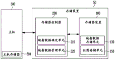
图1是图示根据本公开的实施例的存储装置50的框图。FIG. 1 is a block diagram illustrating a
参考图1,存储装置50可以包括存储器装置100和存储器控制器200。Referring to FIG. 1 , the
存储装置50可以是被配置为在主机300(诸如蜂窝电话、智能电话、MP3播放器、膝上型计算机、台式计算机、游戏机、电视(TV)、平板个人计算机(PC)或车载信息娱乐系统)的控制下存储数据的装置。The
根据作为与主机300通信的通信系统的主机接口,存储装置50可以被制造为各种类型的存储装置中的任一个。例如,数据存储装置50可以被配置为各种类型的存储装置(诸如SSD、MMC、eMMC、RS-MMC或micro-MMC类型的多媒体卡、SD、mini-SD、micro-SD类型的安全数字卡、通用串行总线(USB)存储装置、通用闪存(UFS)装置、个人计算机存储器卡国际协会(PCMCIA)卡类型的存储装置、外围部件互连(PCI)卡类型的存储装置、PCI-快速(PCI-E)类型的存储装置、紧凑型闪存(CF)卡、智能媒体卡和记忆棒)中的任一个。The
存储装置50可以以各种封装类型中的任一个的形式来被制造。例如,可以以各种封装类型(诸如层叠封装(POP)类型、系统级封装(SIP)类型、片上系统(SOC)类型、多芯片封装(MCP)类型、板上芯片(COB)类型、晶圆级制造封装(WFP)类型和晶圆级堆叠封装(WSP)类型)中的任一个的形式来制造存储装置50。The
存储器控制器200可以控制存储装置50的整体操作。The
当对存储装置50供电时,存储器控制器200可以执行固件。在存储器装置100是闪存装置的情况下,存储器控制器200可以执行诸如闪存转换层(FTL)的固件,以用于控制主机300与存储器装置100之间的通信。The
存储器控制器200可以包括映射数据确定单元210。映射数据确定单元210可以从主机300接收映射数据生成请求MG_REQ。映射数据生成请求MG_REQ可以是扩展映射数据请求。扩展映射数据请求可以是用于生成或读取扩展映射数据的请求。扩展映射数据可以包括指示逻辑块地址LBA和物理块地址PBA之间的映射关系的映射信息以及附加字段信息。附加字段信息可以包括关于逻辑块地址LBA和物理块地址PBA之间的映射关系已被更新的次数的信息和/或用于扩展映射数据的纠错的信息。扩展映射数据可以是包括热数据区域的逻辑块地址LBA的数据。可以基于主机300对逻辑块地址LBA的访问频率来确定热数据区域。例如,当针对某个逻辑块地址的访问频率相对较高(或大于阈值)时,与该某个逻辑块地址相对应的区域可以是热数据区域。相反,当针对某个逻辑块地址的访问频率相对较低时,与该某个逻辑块地址相对应的区域可以是冷数据区域。The
映射数据确定单元210可以基于存储器控制器200的内部操作或从主机300接收的数据生成请求MG_REQ,接收与多个扩展映射数据相对应的映射段的位图信息BM_INF。在各个实施例中,映射数据确定单元210可以接收与存储器控制器200的内部操作或从主机300接收的数据生成请求MG_REQ相对应的扩展映射数据所属的映射段的位图信息BM_INF。每个映射段可以包括多个扩展映射数据。位图信息BM_INF可以包括关于映射段的信息。即,位图信息BM_INF可以包括关于与映射段相对应的多个扩展映射数据的信息。在各个实施例中,位图信息BM_INF可以包括关于多个扩展映射数据的生成是否已完成以及扩展映射数据被存储的位置的信息。映射数据确定单元210可以将位图信息BM_INF输出到映射数据管理单元220。The map
映射数据管理单元220可以基于位图信息BM_INF来确定是否生成或输出多个扩展映射数据。此外,映射数据管理单元220可以基于位图信息BM_INF来输出与映射数据生成请求MG_REQ相对应的响应。The map
在各个实施例中,如果从主机300接收的请求是用于生成多个扩展映射数据的请求,则映射数据管理单元220可以生成并且输出多个扩展映射数据。备选地,如果从主机300接收的请求是用于读取多个扩展映射数据的请求,则映射数据管理单元220可以从存储器装置100读取多个扩展映射数据并且将它们输出到主机300。In various embodiments, if the request received from the
存储器装置100可以在其中存储数据。存储器装置100可以在存储器控制器200的控制下操作。存储器装置100可以包括存储器单元阵列,存储器单元阵列包括被配置为在其中存储数据的多个存储器单元。存储器单元阵列可以包括多个存储器块。每个存储器块可以包括多个存储器单元。每个存储器块可以包括多个页。在一个实施例中,每个页可以是在存储器装置100中存储数据或从存储器装置100读取所存储的数据的单位。每个存储器块可以是擦除数据的单位。The
在一个实施例中,存储器装置100可以是双倍数据速率同步动态随机存取存储器(DDR SDRAM)、低功率双倍数据速率4(LPDDR4)SDRAM、图形双倍数据速率(GDDR)SDRAM、低功率DDR(LPDDR)、Rambus动态随机存取存储器(RDRAM)、NAND闪存、垂直NAND闪存、NOR闪存装置、电阻式随机存取存储器(RRAM)、相变存储器(PRAM)、磁阻随机存取存储器(MRAM)、铁电随机存取存储器(FRAM)或自旋转移力矩随机存取存储器(STT-RAM)。在本说明书中,存储器装置100是NAND闪存。In one embodiment,
在一个实施例中,存储器装置100可以体现为三维阵列结构。本公开不仅可以应用于其中电荷存储层由导电浮栅(FG)形成的闪存,而且可以应用于其中电荷存储层由绝缘层形成的电荷陷阱闪存(CTF)。In one embodiment, the
在一个实施例中,存储器装置100中的每个存储器单元可以由能够存储一位数据的单级单元(SLC)形成。备选地,存储器装置100中包括的每个存储器单元可以由能够存储两位数据的多级单元(MLC)形成、由能够存储三位数据的三级单元(TLC)形成或由能够存储四位数据的四级单元(QLC)形成。In one embodiment, each memory cell in
存储器装置100可以从存储器控制器200接收命令和地址,并且访问存储器单元阵列中由地址选择的区域。换言之,存储器装置100可以在由地址选择的区域上执行与命令相对应的操作。例如,存储器装置100可以执行写入(或编程)操作、读取操作和擦除操作。在编程操作期间,存储器装置100可以将数据编程到由地址选择的区域。在读取操作期间,存储器装置100可以从由地址选择的区域读取数据。在擦除操作期间,存储器装置100可以从由地址选择的区域擦除数据。The
存储器装置100可以在存储器控制器200的控制下使用设定的操作电压来执行编程操作或擦除操作。The
存储器装置100可以包括映射数据存储单元130。映射数据存储单元130可以接收由映射数据管理单元220生成的扩展映射数据。扩展映射数据可以是响应于存储器控制器200的内部操作或主机300的映射数据生成请求而生成的映射数据。映射数据存储单元130可以从映射数据管理单元220接收与映射段相对应的扩展映射数据。与映射段相对应的扩展映射数据的数目可以变化。换言之,如果映射数据管理单元220生成映射段中的多个扩展映射数据的全部,则映射段中的扩展映射数据可以被存储在映射数据存储单元130中。The
在各个实施例中,如果映射数据管理单元220生成与映射段相对应的多个扩展映射数据的全部,则映射数据存储单元130可以从映射数据管理单元220接收与映射段相对应的多个扩展映射数据。映射数据存储单元130可以存储所接收的扩展映射数据。In various embodiments, if the mapping
映射数据存储单元130可以响应于存储器控制器200的请求,输出映射数据存储单元130中的多个扩展映射数据。多个扩展映射数据可以是与映射段相对应的数据。在一个实施例中,如果一个映射段中的多个扩展映射数据的全部被输出,则后续映射段中的多个扩展映射数据可以被输出。The map
存储器装置100可以包括位图存储单元150。位图存储单元150可以存储位图。位图可以针对每个映射段而被设置。即,位图可以针对包括多个扩展映射数据的每个映射段而存在。位图存储单元150可以包括与多个相应映射段相对应的判定位。在存储器装置100的初始操作期间,判定位可以被存储在位图存储单元150中。判定位可以被设置为默认值。此后,如果映射段中的映射数据被分配,则对应的判定位可以在与相关联的映射段相对应的映射数据已生成之后被更新。The
位图可以包括关于判定位和存储位置的信息。判定位可以是指示与映射段相对应的多个扩展映射数据的全部是否已生成的位。存储位置可以指示与映射段相对应的多个扩展映射数据已被存储的位置。Bitmaps can include information about decision bits and storage locations. The decision bit may be a bit indicating whether or not all of the plurality of extended map data corresponding to the map segment have been generated. The storage location may indicate a location where a plurality of extended map data corresponding to the map segment have been stored.
如果与映射段相对应的位图尚未存储在位图存储单元150中,则位图存储单元150可以响应于存储器控制器200的请求来生成位图。在初始阶段生成的位图可以针对每个映射段而被设置为默认值。默认值可以被设置为逻辑低电平“0”或逻辑高电平“1”。因此,在存储器控制器200已生成与主机300的请求相对应的映射段中的多个扩展映射数据的全部的情况下,位图可以被更新。在各种实施例中,判定位可以从默认值改变为特定值。附加地,存储位置可以改变为指示针对其中多个扩展映射数据已被存储的存储器块和存储器块中的对应页的地址。If the bitmap corresponding to the mapped segment has not been stored in the
在一个实施例中,存储器控制器200可以从主机300接收数据和逻辑块地址LBA,并且将逻辑块地址LBA转换为物理块地址PBA,物理块地址PBA指示待在其中存储数据的存储器单元的地址,存储器单元被包括在存储器装置100中。附加地,存储器控制器200可以将指示逻辑块地址LBA和物理块地址PBA之间的映射关系的映射信息存储在缓冲器存储器(未示出)中。在一个实施例中,缓冲器存储器可以在存储器控制器200内实现。In one embodiment, the
存储器控制器200可以响应于来自主机300的请求来控制存储器装置100执行编程操作、读取操作或擦除操作。在编程操作期间,存储器控制器200可以向存储器装置100提供编程命令、物理块地址PBA和数据。在读取操作期间,存储器控制器200可以向存储器装置100提供读取命令和物理块地址PBA。在擦除操作期间,存储器控制器200可以向存储器装置100提供擦除命令和物理块地址PBA。The
在一个实施例中,存储器控制器200可以在没有来自主机300的请求的情况下,自主地生成编程命令、地址和数据,并且将它们发送到存储器装置100。例如,存储器控制器200可以向存储器装置100提供命令、地址和数据以执行后台操作,诸如用于耗损均衡的编程操作和用于垃圾收集的编程操作。In one embodiment, the
在一个实施例中,存储器控制器200可以控制至少两个或更多个存储器装置100。在这种情况下,存储器控制器200可以以交错的方式来控制存储器装置100,以增强操作性能。In one embodiment, the
主机300可以使用各种通信方法(诸如通用串行总线(USB)、串行AT附件(SATA)、串行附件SCSI(SAS)、高速芯片间(HSIC)、小型计算机系统接口(SCSI)、外围部件互连(PCI)、PCI快速(PCIe)、非易失性存储器快速(NVMe)、通用闪存(UFS)、安全数字(SD)、多媒体卡(MMC)、嵌入式MMC(eMMC)、双列直插式存储器模块(DIMM)、注册DIMM(RDIMM)和降低负载的DIMM(LRDIMM)通信方法)中的至少一个来与存储装置50通信。The
主机300可以包括主机存储器310。主机存储器310可以存储从映射数据管理单元220接收的多个扩展映射数据。多个扩展映射数据可以是响应于主机300的请求而通过存储器控制器200已被存储在存储器装置100中或从存储器装置100读取的数据。在各个实施例中,在基于存储器控制器200的内部操作或主机300的映射数据生成请求MG_REQ来将多个扩展映射数据存储在存储器装置100中之后,可以基于主机300的映射数据读取请求MR_REQ来将存储器装置100中的多个扩展映射数据存储在主机存储器310中。Host 300 may include
待存储在主机存储器310中的多个扩展映射数据可以基于映射段来被存储。映射段可以对应于多个扩展映射数据。即,每个映射段可以包括多个扩展映射数据。在一个实施例中,如果与一个映射段相对应的多个扩展映射数据被存储在主机存储器310中,则与后续的映射段相对应的多个扩展映射数据可以存储在主机存储器310中。A plurality of extended map data to be stored in the
图2是图示根据本公开的实施例的存储器控制器(例如,图1的存储器控制器200)的图。FIG. 2 is a diagram illustrating a memory controller (eg,
参考图2,存储器控制器200可以包括映射数据确定单元210和映射数据管理单元220。Referring to FIG. 2 , the
映射数据确定单元210可以从主机300接收映射数据生成请求MG_REQ(①)。映射数据生成请求MG_REQ可以是扩展映射数据请求。扩展映射数据请求可以是用于生成或读取扩展映射数据的请求。映射数据生成请求MG_REQ可以是用于生成单个或多个扩展映射数据的请求。扩展映射数据可以包括指示逻辑块地址LBA和物理块地址PBA之间的映射关系的映射信息以及附加字段信息。附加字段信息可以包括关于扩展映射数据已被更新的次数的信息和/或用于扩展映射数据的纠错的信息。用于纠错的信息可以包括纠错位。纠错位可以是奇偶校验位。奇偶校验位可以是被添加以检查在信息传输过程期间是否已发生错误的位。The map
映射数据确定单元210可以基于从主机300接收的映射数据生成请求MG_REQ来将位图请求BM_REQ输出到存储器装置100(②)。映射数据确定单元210可以接收与位图请求BM_REQ相对应的位图信息BM_INF(③),并且基于位图信息BM_INF来确定是否生成扩展映射数据。The map
在各个实施例中,为了接收用于确定是否基于存储器控制器200的内部操作或映射数据生成请求MG_REQ来生成扩展映射数据的位图信息BM_INF,映射数据确定单元210可以向存储器装置100输出位图请求BM_REQ。位图信息BM_INF可以包括判定位和存储位置。判定位可以指示与映射段相对应的多个扩展映射数据是否已生成。存储位置可以指示与主机300的请求相对应的多个扩展映射数据存储在存储器装置100中的地址。位图信息BM_INF可以基于映射段被存储在存储器装置100中。映射段可以是与多个扩展映射数据相对应的单位。每个映射段可以包括多个扩展映射数据。每个映射段中的扩展映射数据的数目可以变化。In various embodiments, in order to receive bitmap information BM_INF for determining whether to generate extended map data based on an internal operation of the
存储器装置100可以输出与映射段对应的位图信息BM_INF(③)。映射段可以包括多个扩展映射数据。在一个实施例中,映射段可以包括与从主机300接收的请求相对应的扩展映射数据。在一个实施例中,映射段可以包括与存储器控制器200的内部操作相对应的扩展映射数据。The
位图信息BM_INF可以包括关于存储在位图存储单元150中的位图的信息。位图可以包括与多个映射段中的每一个相对应的判定位。判定位可以指示对应的映射段中的多个扩展映射数据的全部是否已生成。在一个实施例中,判定位可以是逻辑低电平“0”或逻辑高电平“1”。The bitmap information BM_INF may include information on bitmaps stored in the
在各个实施例中,在映射段中的多个扩展映射数据的全部尚未存储在存储器装置100中的情况下,判定位可以为“0”。备选地,在映射段中的多个扩展映射数据的全部已被存储在存储器装置100中的情况下,判定位可以是“1”。In various embodiments, where all of the plurality of extended map data in the map segment has not been stored in the
在判定位是“0”的情况下,判定位可以从“0”被更新为“1”。在一个实施例中,如果判定位的默认值是“1”,则在映射段中包括的多个扩展映射数据的全部已生成之后,判定位可以从“1”被更新为“0”。In the case where the determination bit is "0", the determination bit may be updated from "0" to "1". In one embodiment, if the default value of the predicate bit is '1', the predicate bit may be updated from '1' to '0' after all of the plurality of extended map data included in the map segment have been generated.
在该图中,从存储器装置100接收的位图信息BM_INF指示映射段中的多个扩展映射数据的全部尚未被存储。扩展映射数据可以是与从主机300接收的请求相对应的映射数据。备选地,扩展映射数据可以是在没有主机300的请求的情况下生成的映射数据。In this figure, the bitmap information BM_INF received from the
映射数据确定单元210可以基于从存储器装置100接收的位图信息BM_INF来输出生成信息GE_INF(④)。生成信息GE_INF可以包括用于生成位图信息BM_INF和扩展映射数据的信息。The mapping
在各个实施例中,在位图信息BM_INF指示与映射段相对应的多个扩展映射数据的全部尚未生成的情况下,映射数据确定单元210可以输出用于生成位图的生成信息GE_INF。另外,在位图信息BM_INF指示与映射段相对应的多个扩展映射数据的全部尚未生成的情况下,生成信息GE_INF可以包括用于生成多个扩展映射数据的信息。相反,在位图信息BM_INF指示与映射段相对应的多个扩展映射数据的全部已生成的情况下,生成信息GE_INF可以包括指示多个扩展映射数据已生成的信息。In various embodiments, in a case where the bitmap information BM_INF indicates that all of the plurality of extended map data corresponding to the map segment have not been generated, the map
映射数据管理单元220可以从映射数据确定单元210接收生成信息GE_INF(④)。映射数据管理单元220可以基于生成信息GE_INF来生成位图和/或扩展映射数据。The map
在一个实施例中,在尚未从存储器装置100接收位图信息BM_INF的情况下,映射数据管理单元220可以将用于生成位图的位图生成命令BG_CMD输出到存储器装置100(⑤)。存储器装置100可以生成与位图生成命令BG_CMD相对应的位图。在各种实施例中,存储器装置100可以生成包括判定位和存储位置的位图。当生成位图时,判定位和存储位置各自可以具有默认值。默认值可以是“0”或“1”。In one embodiment, in the case where the bitmap information BM_INF has not been received from the
映射数据管理单元220可以在位图已生成之后生成扩展映射数据。在各种实施例中,映射数据管理单元220可以基于映射段来生成扩展映射数据。映射段可以包括多个扩展映射数据。如果生成了映射段中的多个扩展映射数据,则映射数据管理单元220可以将所生成的扩展映射数据输出到存储器装置100。The map
图3A和图3B是图示根据本公开的实施例的响应于主机(例如,图1和图2的主机300)的请求而生成的正常映射数据和扩展映射数据的图。3A and 3B are diagrams illustrating normal map data and extended map data generated in response to a request of a host (eg, host 300 of FIGS. 1 and 2 ) according to an embodiment of the present disclosure.
参考图3A和图3B,可以由存储器控制器200响应于主机300的请求来生成映射数据。映射数据的类型可以是正常映射数据和扩展映射数据中的任一个。图3A图示了正常映射数据的示例。图3B图示了扩展映射数据的示例。Referring to FIGS. 3A and 3B , map data may be generated by the
参考图3A,可以响应于主机300的映射数据生成请求MG_REQ来生成正常映射数据。正常映射数据可以包括指示逻辑块地址LBA和物理块地址PBA之间的映射关系的映射信息。正常映射数据可以不包括附加字段信息。Referring to FIG. 3A , normal map data may be generated in response to a map data generation request MG_REQ of the
第一映射数据Mapping_DATA1和第二映射数据Mapping_DATA2可以是正常映射数据。换言之,图2的映射数据管理单元220可以基于从主机300接收的映射数据生成请求MG_REQ来生成第一映射数据Mapping_DATA1和第二映射数据Mapping_DATA2。在一个实施例中,可以增加由映射数据管理单元220生成的正常映射数据的数目。The first mapping data Mapping_DATA1 and the second mapping data Mapping_DATA2 may be normal mapping data. In other words, the mapping
第一映射数据Mapping_DATA1和第二映射数据Mapping_DATA2中的每一个可以包括指示逻辑块地址LBA和物理块地址PBA之间的映射关系的映射信息。在一个实施例中,第一映射数据Mapping_DATA1可以包括指示第一逻辑块地址LBA1和第一物理块地址PBA1之间的映射关系的映射信息。第二映射数据Mapping_DATA2可以包括指示第二逻辑块地址LBA2和第二物理块地址PBA2之间的映射关系的映射信息。Each of the first mapping data Mapping_DATA1 and the second mapping data Mapping_DATA2 may include mapping information indicating a mapping relationship between the logical block address LBA and the physical block address PBA. In one embodiment, the first mapping data Mapping_DATA1 may include mapping information indicating a mapping relationship between the first logical block address LBA1 and the first physical block address PBA1. The second mapping data Mapping_DATA2 may include mapping information indicating a mapping relationship between the second logical block address LBA2 and the second physical block address PBA2.
参考图3B,可以响应于存储器控制器200的内部操作或主机300的映射数据生成请求MG_REQ而生成扩展映射数据。映射数据生成请求MG_REQ可以基于关于热数据区域的热数据信息来从主机300被接收。可以基于主机300对逻辑块地址LBA的访问频率来确定热数据区域。例如,当针对某个逻辑块地址的访问频率相对较高(或大于阈值)时,与该某个逻辑块地址相对应的区域可以是热数据区域。相反,当针对某个逻辑块地址的访问频率相对较低时,与该某个逻辑块地址相对应的区域可以是冷数据区域。映射数据生成请求MG_REQ可以是用于生成扩展映射数据的请求。Referring to FIG. 3B , extended map data may be generated in response to an internal operation of the
映射数据管理单元220可以基于映射数据生成请求MG_REQ来生成扩展映射数据。扩展映射数据可以包括指示逻辑块地址LBA和物理块地址PBA之间的映射关系的映射信息以及附加字段信息。正常映射数据可以包括指示逻辑块地址LBA和物理块地址PBA之间的映射关系的映射信息。换言之,扩展映射数据可以是包括正常映射数据和附加字段信息的数据。The map
扩展映射数据可以被输出到主机300。主机300可以将扩展映射数据存储在主机存储器310中。此后,主机300可以将操作请求和与操作请求相对应的扩展映射数据输出到存储器控制器200。存储器控制器200可以基于操作请求和与操作请求相对应的扩展映射数据来控制待在存储器装置100中执行的操作。The extended map data may be output to the
在一个实施例中,第三映射数据Mapping_DATA3和第四映射数据Mapping_DATA4可以是扩展映射数据。即,映射数据管理单元220可以基于从主机300接收的映射数据生成请求MG_REQ来生成第三映射数据Mapping_DATA3和第四映射数据Mapping_DATA4。在一个实施例中,由映射数据管理单元220生成的扩展映射数据的数目可以增加。In one embodiment, the third mapping data Mapping_DATA3 and the fourth mapping data Mapping_DATA4 may be extended mapping data. That is, the mapping
第三映射数据Mapping_DATA3和第四映射数据Mapping_DATA4中的每一个可以包括指示逻辑块地址LBA和物理块地址PBA之间的映射关系的映射信息以及附加字段信息k3、k4。在一个实施例中,第三映射数据Mapping_DATA3和第四映射数据Mapping_DATA4中的每一个可以包括正常映射数据和附加字段信息。Each of the third mapping data Mapping_DATA3 and the fourth mapping data Mapping_DATA4 may include mapping information indicating a mapping relationship between the logical block address LBA and the physical block address PBA, and additional field information k3, k4. In one embodiment, each of the third mapping data Mapping_DATA3 and the fourth mapping data Mapping_DATA4 may include normal mapping data and additional field information.
第三映射数据Mapping_DATA3可以包括指示第三逻辑块地址LBA3和第三物理块地址PBA3之间的映射关系的映射信息以及附加字段信息k3。第四映射数据Mapping_DATA4可以包括指示第四逻辑块地址LBA4和第四物理块地址PBA4之间的映射关系的映射信息以及附加字段信息k4。第三映射数据Mapping_DATA3和第四映射数据Mapping_DATA4中的附加字段信息k3和k4可以各自存储逻辑块地址和物理块地址之间的映射信息的更新次数或用于纠错的数据(例如,Bose-Chaudhuri-Hocquenghem码(BCH码)、低密度奇偶校验码(LDPC码等))。用于纠错的数据可以包括纠错位。纠错位可以是奇偶校验位。奇偶校验位可以是被添加以检查在信息传输过程期间是否已发生错误的位。The third mapping data Mapping_DATA3 may include mapping information indicating a mapping relationship between the third logical block address LBA3 and the third physical block address PBA3 and additional field information k3. The fourth mapping data Mapping_DATA4 may include mapping information indicating a mapping relationship between the fourth logical block address LBA4 and the fourth physical block address PBA4 and additional field information k4. The additional field information k3 and k4 in the third mapping data Mapping_DATA3 and the fourth mapping data Mapping_DATA4 may each store the number of updates of the mapping information between the logical block address and the physical block address or data for error correction (for example, Bose-Chaudhuri - Hocquenghem codes (BCH codes), low density parity check codes (LDPC codes, etc.)). Data for error correction may include error correction bits. The error correction bits may be parity bits. Parity bits may be bits that are added to check whether an error has occurred during the information transmission process.
在一个实施例中,在扩展映射数据已被更新的次数被存储在附加字段信息中的情况下,映射数据管理单元220可以基于附加字段信息中的数据来确定待输出到存储器装置100的映射数据。在一个实施例中,在用于校正扩展映射数据中的错误的数据被包括在附加字段信息中的情况下,存储器控制器200可以基于附加字段信息中的数据来执行对扩展映射数据中已发生的错误进行校正的操作。In one embodiment, in the case where the number of times the extended map data has been updated is stored in the additional field information, the map
图4A和图4B是图示根据本公开的实施例的待存储在图2的存储器装置100中的位图的图。4A and 4B are diagrams illustrating bitmaps to be stored in the
图4A图示了最初存储在存储器装置100中的位图。图4B图示了存储在存储器装置100中的位图的初始存储位置。位图和存储位置均可以对应于映射段。映射段可以包括多个扩展映射数据。此外,主机性能增强器(HPB)映射数据可以包括多个映射段。FIG. 4A illustrates a bitmap initially stored in
在一个实施例中,判定位的默认值可以被包括在最初存储在存储器装置100中的位图中。判定位的默认值可以是“0”或“1”。在该图中,判定位的默认值为“0”。In one embodiment, the default value of the decision bit may be included in a bitmap originally stored in the
图4B图示了映射段中的多个扩展映射数据被存储的初始位置。在映射段中的多个扩展映射数据生成之前,与映射段相对应的存储位置的值可以是默认值。在图4B中,存储位置的默认值为“0”。FIG. 4B illustrates the initial location where a plurality of extended map data in the map segment are stored. The value of the storage location corresponding to the map segment may be a default value before the plurality of extended map data in the map segment is generated. In Figure 4B, the default value of the storage location is "0".
在一个实施例中,在尚未从存储器装置100接收位图信息BM_INF的情况下,映射数据管理单元220可以将用于生成位图的位图生成命令BG_CMD输出到存储器装置100。图4A图示了由存储器装置100响应于位图生成命令BG_CMD而生成的初始位图。In one embodiment, in the case where the bitmap information BM_INF has not been received from the
在各个实施例中,可以基于映射段来生成位图。图4A和图4B图示了与第一映射段Map_Segment1和第二映射段Map_Segment2相对应的位图的初始生成。在一个实施例中,存储器装置100可以接收位图生成命令BG_CMD,并且基于位图生成命令BG_CMD来生成与更大数目的映射段相对应的位图。In various embodiments, the bitmap may be generated based on the map segment. 4A and 4B illustrate the initial generation of bitmaps corresponding to the first map segment Map_Segment1 and the second map segment Map_Segment2. In one embodiment, the
映射段可以是包括多个扩展映射数据的单位。在各个实施例中,每个映射段可包括至少两个或更多个扩展映射数据。在一个实施例中,基于与从主机300接收的映射数据生成请求相对应的扩展映射数据的数目,可以设置包括扩展映射数据的映射段。换言之,可以基于待由存储器控制器200生成的扩展映射数据的数目来设置映射段。A map segment may be a unit including a plurality of extended map data. In various embodiments, each map segment may include at least two or more extended map data. In one embodiment, based on the number of extended map data corresponding to the map data generation request received from the
在一个实施例中,可以生成分别对应于第一映射段Map_Segment1和第二映射段Map_Segment2的位图。判定位可以指示与存储器控制器200的内部操作或从主机300接收的映射数据生成请求MG_REQ相对应的扩展映射数据是否已生成。In one embodiment, bitmaps corresponding to the first map segment Map_Segment1 and the second map segment Map_Segment2, respectively, may be generated. The decision bit may indicate whether extended map data corresponding to an internal operation of the
基于位图生成命令BG_CMD生成的位图中的判定位可以在初始阶段被设置为默认值。默认值可以是“0”或“1”。在图4A中,默认值为“0”。Decision bits in the bitmap generated based on the bitmap generation command BG_CMD may be set to default values at the initial stage. The default value can be "0" or "1". In Figure 4A, the default value is "0".
如果与映射段相对应的多个扩展映射数据的全部均已生成,则可以更新判定位。在各种实施例中,如果映射段中的多个扩展映射数据的全部已生成,则可以将判定位从“0”更新为“1”。在一个实施例中,如果判定位的默认值为“1”,则在映射段中的多个扩展映射数据的全部已生成之后,可以将判定位从“1”更新为“0”。The decision bit may be updated if all of the plurality of extended map data corresponding to the map segment have been generated. In various embodiments, the decision bit may be updated from "0" to "1" if all of the plurality of extended map data in the map segment have been generated. In one embodiment, if the default value of the predicate bit is "1", the predicate bit may be updated from "1" to "0" after all of the multiple extended map data in the mapped segment have been generated.
在一个实施例中,对应于映射段的存储位置可以存储在存储器装置100中。例如,存储位置可以存储在作为存储器装置100的非易失性存储器中。存储位置可以指示其中与存储器控制器200的内部操作或从主机300接收的映射数据生成请求MG_REQ相对应的扩展映射数据被存储的地址。扩展映射数据被存储的地址可以是存储器块的地址和存储器块中的页。In one embodiment, storage locations corresponding to mapped segments may be stored in
存储位置可以指示映射段中的多个扩展映射数据已被存储的位置。如果映射段中的多个扩展映射数据的全部已生成,则可以更新存储位置。The storage location may indicate a location in the map segment where the plurality of extended map data has been stored. If all of the multiple extended map data in the map segment have been generated, the storage location can be updated.
在一个实施例中,基于位图生成命令BG_CMD生成的存储位置可以被设置为默认值。默认值可以是“0”或“1”。在图4B中,默认值为“0”。此后,如果与映射段相对应的多个扩展映射数据的全部已生成,则可以更新存储位置。In one embodiment, the storage location generated based on the bitmap generation command BG_CMD may be set as a default value. The default value can be "0" or "1". In Figure 4B, the default value is "0". Thereafter, if all of the plurality of extended map data corresponding to the map segment have been generated, the storage location may be updated.
在各个实施例中,如果映射段中的多个扩展映射数据的全部已生成,则可以将存储位置更新为其中已存储扩展映射数据的存储器块的地址和存储器块中对应页的地址。存储位置可以包括关于在存储器单元阵列中的多个存储器块之中的已存储扩展映射数据的存储器块的位置和存储器块中对应页的位置的信息。In various embodiments, if all of the plurality of extended map data in the map segment have been generated, the storage location may be updated to the address of the memory block in which the extended map data has been stored and the address of the corresponding page in the memory block. The storage location may include information on the location of the memory block in which the extension map data has been stored among the plurality of memory blocks in the memory cell array and the location of the corresponding page in the memory block.
图5是图示根据本公开的实施例的在与映射段相对应的映射数据的生成已完成之后的存储器控制器200的操作的图。FIG. 5 is a diagram illustrating the operation of the
参考图5,存储器控制器200可以包括映射数据管理单元220。在该图中,省略了存储器控制器200中的映射数据确定单元210。Referring to FIG. 5 , the
例如,图5图示了在与从主机300接收的映射数据生成请求MG_REQ或存储器控制器200的内部操作相对应的多个扩展映射数据已生成之后的操作。在一个实施例中,映射数据管理单元220可以基于映射段来生成扩展映射数据。如果生成了映射段中的多个扩展映射数据,则映射数据管理单元220可以执行将多个扩展映射数据存储在存储器装置100中的操作。For example, FIG. 5 illustrates operations after a plurality of extended map data corresponding to the map data generation request MG_REQ received from the
在一个实施例中,映射数据管理单元220可以将映射段编程命令MSP_CMD输出到存储器装置100。映射段编程命令MSP_CMD可以是用于将由映射数据管理单元220生成的多个扩展映射数据存储在存储器装置100中的命令。In one embodiment, the map
在各个实施例中,如果多个扩展映射数据的生成已完成,则映射数据管理单元220可以将映射段编程命令MSP_CMD输出到存储器装置100。每当映射段中的扩展映射数据的生成完成时,可以输出用于存储与映射段相对应的扩展映射数据的命令。在一个实施例中,如果完成了一个映射段中的扩展映射数据的生成,则与映射段相对应的扩展映射数据存储在存储器装置100中。随后,映射数据管理单元220可以生成与后续映射段相对应的扩展映射数据。In various embodiments, the map
在一个实施例中,映射数据管理单元220可以将位图编程命令BMP_CMD输出到存储器装置100。可以在与映射段编程命令BMP_CMD相对应的多个扩展映射数据的全部已存储在存储器装置100中之后,输出位图编程命令MSP_CMD。可以在输出映射段编程命令MSP_CMD之后,输出位图编程命令BMP_CMD。存储器装置100可以接收位图编程命令BMP_CMD并且更新位图。In one embodiment, the map
在各个实施例中,可以更新位图以指示与映射段相对应的多个扩展映射数据的全部均已存储。如果存储器装置100接收位图编程命令BMP_CMD,则可以更新与存储在存储器装置100中的映射段相对应的位图。在一个实施例中,位图中的判定位可以从默认值更新为特定值。此外,关于与映射段相对应的多个扩展映射数据被存储的位置的信息可以被更新。In various embodiments, the bitmap may be updated to indicate that all of the plurality of extended map data corresponding to the map segment are stored. If the
如果存储在存储器装置100中的位图被更新,则映射数据管理单元220可以向主机300输出响应,该响应指示与存储器控制器200的内部操作或从主机300接收的映射数据生成请求MG_REQ相对应的多个扩展映射数据的生成已完成。每当生成与一个映射段相对应的多个扩展映射数据的全部时,可以将对应的响应输出到主机300。从映射数据管理单元220输出的响应可以是生成完成响应GC_RES。在生成完成响应GC_RES已被接收之后,主机300可以将用于读取存储在存储器装置100中的多个扩展映射数据的请求输出到存储器控制器200。If the bitmap stored in the
图6A和图6B是图示根据本公开的实施例的位图上的更新的图。6A and 6B are diagrams illustrating updating on a bitmap according to an embodiment of the present disclosure.
图6A图示了包括与映射段相对应的判定位的位图。图6B图示了与存储在存储器装置100中的映射段相对应的存储位置。映射段可以包括多个扩展映射数据。此外,主机性能增强器(HPB)映射数据可以包括多个映射段。6A illustrates a bitmap including decision bits corresponding to mapped segments. FIG. 6B illustrates storage locations corresponding to mapped segments stored in the
在一个实施例中,基于存储器控制器200的内部操作或从主机300接收的映射数据生成请求MG_REQ,可以生成映射段中的多个扩展映射数据。In one embodiment, a plurality of extended map data in the map segment may be generated based on the internal operation of the
在一个实施例中,在与存储器控制器200的内部操作或从主机300接收的请求相对应的扩展映射数据尚未存储在存储器装置100中的情况下,可以设置用于生成扩展映射数据的映射段。可以根据每个映射段中可以包括的扩展映射数据的最大数目来确定映射段的数目。可以根据响应于从主机300接收的请求而生成的扩展映射数据的数目来确定映射段的数目。In one embodiment, in the case where the extended map data corresponding to the internal operation of the
与映射段相对应的扩展映射数据的数目可以变化。例如,一个映射段包括四个扩展映射数据。此外,位图信息中包括的位对应于一个映射段。即,四个扩展映射数据对应于位图信息中包括的一个位。The number of extended map data corresponding to the map segment may vary. For example, one map segment includes four extended map data. Also, the bits included in the bitmap information correspond to one map segment. That is, four extended map data correspond to one bit included in the bitmap information.
在图6A和图6B中,与每个映射段相对应的扩展映射数据的数目为四个。因此,如果响应于从主机300接收的映射数据生成请求MG_REQ而待生成的扩展映射数据的数目为八个,则可以将映射段的数目设置为两个。In FIGS. 6A and 6B , the number of extended map data corresponding to each map segment is four. Therefore, if the number of extended map data to be generated in response to the map data generation request MG_REQ received from the
映射数据管理单元220可以从映射数据确定单元210接收生成信息GE_INF并且生成扩展映射数据。生成信息GE_INF可以包括指示与存储器控制器200的内部操作或从主机300接收的映射数据生成请求MG_REQ相对应的扩展映射数据尚未存储在存储器装置100中的信息。基于生成信息GE_INF,映射数据管理单元220可以生成与存储器控制器200的内部操作或映射数据生成请求MG_REQ相对应的扩展映射数据。The map
在一个实施例中,存储器控制器200的内部操作或从主机300接收的映射数据生成请求MG_REQ可以是用于顺序地生成多个映射数据的请求。在各种实施例中,从主机300接收的映射数据生成请求MG_REQ可以是用于生成随机映射数据的请求。在从主机300接收的请求是用于生成随机映射数据的请求的情况下,可以按照所请求的顺序来设置用于生成扩展映射数据的映射段。In one embodiment, the internal operation of the
映射数据管理单元220可以生成与第一映射段Map_Segment1相对应的扩展映射数据。在与第一映射段Map_Segment1相对应的多个扩展映射数据已生成之后,可以生成与第二映射段Map_Segment2相对应的多个扩展映射数据。The map
如果映射数据管理单元220生成与第一映射段Map_Segment1相对应的多个扩展映射数据的全部,则位图可以被更新。在各个实施例中,如果生成了与第一映射段Map_Segment1相对应的多个扩展映射数据的全部,则映射数据管理单元220可以将用于在存储器装置100中存储与第一映射段Map_Segment1相对应的扩展映射数据的映射段编程命令MSP_CMD输出到存储器装置100。If the map
在与第一映射段Map_Segment1相对应的多个扩展映射数据的全部存储在存储器装置100中之后,映射数据管理单元220可以将位图编程命令BMP_CMD输出到存储器装置100,以更新对应于第一映射段Map_Segment1的位图。存储器装置100可以接收位图编程命令BMP_CMD并且更新位图。在一个实施例中,可以更新位图中包括的判定位和存储位置。After all of the plurality of extension map data corresponding to the first map segment Map_Segment1 are stored in the
判定位可以是指示与映射段相对应的多个扩展映射数据的全部是否已生成的位。此外,存储位置可以指示与映射段相对应的多个扩展映射数据已被存储的位置。The decision bit may be a bit indicating whether or not all of the plurality of extended map data corresponding to the map segment have been generated. Also, the storage location may indicate a location where a plurality of extended map data corresponding to the map segment have been stored.
参考6A,为了指示与第一映射段Map_Segment1相对应的多个扩展映射数据的全部已生成,可以将判定位从默认值改变为特定值。Referring to 6A, in order to indicate that all of the plurality of extended map data corresponding to the first map segment Map_Segment1 have been generated, the decision bit may be changed from a default value to a specific value.
例如,由于判定位的默认值为“0”,在与第一映射段Map_Segment1相对应的多个映射数据的全部已生成之后,与第一映射段Map_Segment1相对应的判定位可以被更新为“1”。For example, since the default value of the decision bit is "0", the decision bit corresponding to the first map segment Map_Segment1 may be updated to "1" after all of the plurality of map data corresponding to the first map segment Map_Segment1 have been generated ".
参考图6B,与第一映射段Map_Segment1相对应的扩展映射数据的存储位置可以被更新。可以将存储位置从默认值“0”更新为其中已存储与第一映射段Map_Segment1相对应的扩展映射数据的地址。在图6A和图6B中,与第一映射段Map_Segment1相对应的扩展映射数据的地址是第零存储器块Block0的第一页Page1。Referring to FIG. 6B , the storage location of the extended map data corresponding to the first map segment Map_Segment1 may be updated. The storage location may be updated from the default value "0" to the address in which the extended map data corresponding to the first map segment Map_Segment1 has been stored. In FIGS. 6A and 6B , the address of the extended map data corresponding to the first map segment Map_Segment1 is the first page Page1 of the zeroth memory block Block0.
在已生成与第一映射段Map_Segment1相对应的多个扩展映射数据的全部并将其存储在存储器装置100中并且已更新位图之后,映射数据管理单元220可以生成与第二映射段Map_Segment2对应的扩展映射数据。After all of the plurality of extension map data corresponding to the first map segment Map_Segment1 have been generated and stored in the
在图6A和图6B中,与第二映射段Map_Segment2相对应的多个扩展映射数据的全部尚未生成。关于位图中的判定位和存储位置的信息可以被设置为默认值“0”。如果与第二映射段Map_Segment2相对应的多个扩展映射数据的全部已生成,则可以更新与第二映射段Map_Segment2相对应的位图。In FIGS. 6A and 6B , all of the plurality of extended map data corresponding to the second map segment Map_Segment2 have not yet been generated. Information about decision bits and storage locations in the bitmap may be set to a default value of "0". If all of the plurality of extended map data corresponding to the second map segment Map_Segment2 have been generated, the bitmap corresponding to the second map segment Map_Segment2 may be updated.
在一个实施例中,在映射数据管理单元220响应于存储器控制器200的内部操作或主机300的请求而生成扩展映射数据时,存储装置50可能以功率休眠模式操作。功率休眠模式可以意味着存储器装置50以低功率状态操作。如果存储装置50以功率休眠模式操作,则由映射数据管理单元220正在生成的扩展映射数据可能被删除。然而,每当生成对应于映射段的扩展映射数据时,扩展映射数据被存储在存储器装置100中。因此,映射数据管理单元220可以生成除了存储在存储器装置100中的扩展映射数据以外的扩展映射数据。In one embodiment, the
在一个实施例中,当存储装置50以功率休眠模式操作时,由映射数据管理单元220正在生成的并且被包括在第二映射段Map_Segment2中的映射数据可能被删除。然而,由于与第一映射段Map_Segment1相对应的多个扩展映射数据的全部已生成并且存储在存储器装置100中,映射数据管理单元220可以仅生成与第二段相对应的扩展映射数据。即,映射数据管理单元220可以省略与第一映射段Map_Segment1相对应的扩展映射数据的生成。In one embodiment, the map data being generated by the map
因此,如果存储装置50的功率休眠模式结束,则映射数据管理单元220可以接收关于存储在存储器装置100中的位图的位图信息BM_INF,并且基于位图中的判定位来确定是否生成扩展映射数据。Therefore, if the power sleep mode of the
由于位图的判定位指示与映射段相对应的多个扩展映射数据的全部是否已生成,映射数据管理单元220可以基于判定位来确定是否生成扩展映射数据。因此,在映射段中的扩展映射数据的生成尚未完成的情况下,可以再次生成对应的映射段中的扩展映射数据。Since the decision bit of the bitmap indicates whether all of the plurality of extended map data corresponding to the map segment have been generated, the map
因此,在映射数据管理单元220已再次生成第二映射段Map_Segment2中的多个扩展映射数据之后,与第二映射段Map_Segment2相对应的位图可以被更新。Therefore, after the map
图7是图示根据本公开的实施例的在与映射段相对应的映射数据已生成的情况下存储器控制器200的操作的图。FIG. 7 is a diagram illustrating the operation of the
参考图7,存储器控制器200可以包括映射数据确定单元210和映射数据管理单元220。图7图示了在与存储器控制器200的内部操作或主机300的映射数据生成请求MG_REQ相对应的扩展映射数据已被存储在存储器装置100中的情况下存储器控制器200的操作。Referring to FIG. 7 , the
映射数据确定单元210可以从主机300接收映射数据生成请求MG_REQ(①)。映射数据生成请求MG_REQ可以是用于生成扩展映射数据的请求。映射数据生成请求MG_REQ可以是用于生成多个扩展映射数据的请求。扩展映射数据可以包括指示逻辑块地址LBA和物理块地址PBA之间的映射关系的映射信息以及附加字段信息。附加字段信息可以包括关于逻辑块地址LBA和物理块地址PBA之间的映射关系已被更新的次数的信息和/或用于扩展映射数据的纠错的信息。用于纠错的信息可以包括纠错位。纠错位可以是奇偶校验位。奇偶校验位可以是被添加来检查在信息传输过程期间是否已发生错误的位。The map
映射数据确定单元210可以基于存储器控制器200的内部操作或从主机300接收的映射数据生成请求MG_REQ,将位图请求BM_REQ输出到存储器装置100(②)。映射数据确定单元210可以接收与位图请求BM_REQ相对应的位图信息BM_INF(③)。映射数据管理单元210可以接收位图信息BM_INF,并且基于位图信息BM_INF确定是否生成扩展映射数据。The map
在一个实施例中,位图信息BM_INF可以包括关于与映射段相对应的位图的信息。映射段可以对应于多个扩展映射数据。换言之,映射段可以包括多个扩展映射数据。因此,位图信息BM_INF可以包括与至少一个映射段相对应的信息,至少一个映射段包括与存储器控制器200的内部操作或从主机300接收的映射数据生成请求MG_REQ相对应的扩展映射数据。In one embodiment, the bitmap information BM_INF may include information about a bitmap corresponding to a map segment. A map segment may correspond to a plurality of extended map data. In other words, a map segment may include a plurality of extended map data. Accordingly, the bitmap information BM_INF may include information corresponding to at least one map segment including extended map data corresponding to an internal operation of the
位图信息BM_INF可以包括关于对应于映射段的判定位以及存储位置的信息。判定位可以是指示与映射段相对应的多个扩展映射数据的全部是否已生成的位。存储位置可以指示与映射段相对应的多个扩展映射数据已被存储的地址。The bitmap information BM_INF may include information on decision bits and storage locations corresponding to the mapped segments. The decision bit may be a bit indicating whether or not all of the plurality of extended map data corresponding to the map segment have been generated. The storage location may indicate an address where a plurality of extended map data corresponding to the map segment have been stored.
在关于与映射段相对应的位图的信息未存储在存储器装置100中的情况下,位图信息BM_INF可以指示与映射段相对应的多个扩展映射数据的全部尚未生成。在关于与映射段相对应的位图的信息已存储在存储器装置100中的情况下,映射数据确定单元210可以接收包括判定位和存储位置的位图信息BM_INF。In a case where the information on the bitmap corresponding to the map segment is not stored in the
在图7中,与存储器控制器200的内部操作或主机300的映射数据生成请求MG_REQ相对应的扩展映射数据已被存储在存储器装置100中。因此,在输出到存储器装置100的位图信息BM_INF中,与扩展映射数据相对应的至少一个映射段的位图可以包括指示扩展映射数据已存储在存储器装置100中的信息。在各个实施例中,判定位可以具有特定值,并且关于存储位置的信息可以包括关于扩展映射数据被存储的地址的信息。In FIG. 7 , extended map data corresponding to the internal operation of the
映射数据确定单元210可以基于从存储器装置100接收的位图信息BM_INF来输出生成信息GE_INF(④)。在一个实施例中,生成信息GE_INF可以包括指示与存储器控制器200的内部操作或从主机300接收的映射数据生成请求MG_REQ相对应的扩展映射数据已生成的信息。生成信息GE_INF可以包括指示映射数据管理单元220不生成与主机300的请求相对应的扩展映射数据的信息。The mapping
如果映射数据管理单元220从映射数据确定单元210接收生成信息GE_INF,则映射数据管理单元220可以将生成完成响应GC_RES输出到主机300(⑤)。在一个实施例中,生成信息GE_INF可以包括指示与存储器控制器200的内部操作或从主机300接收的映射数据生成请求MG_REQ相对应的多个扩展映射数据的全部已生成的信息。映射数据管理单元220可以向主机300输出生成完成响应GC_RES,生成完成响应GC_RES指示与从主机300接收的请求相对应的多个扩展映射数据的全部已生成。If the map
在已从映射数据管理单元220接收生成完成响应GC_RES之后,主机300可以向存储器控制器200输出用于读取响应于映射数据生成请求MG_REQ而生成的扩展映射数据的请求。After having received the generation completion response GC_RES from the map
图8是图示根据本公开的实施例的将与主机300的请求相对应的映射数据输出到主机300的方法的图。FIG. 8 is a diagram illustrating a method of outputting map data corresponding to a request of the
参考图8,存储器控制器200可以包括映射数据确定单元210和映射数据管理单元220。映射数据确定单元210可以确定与从主机300接收的映射数据读取请求MR_REQ相对应的扩展映射数据是否已被存储在存储器装置100中。映射数据管理单元220可以从存储器装置100接收与主机300的映射数据读取请求MR_REQ相对应的扩展映射数据,并且将扩展映射数据输出到主机300。Referring to FIG. 8 , the
在一个实施例中,映射数据确定单元210可以从主机300接收映射数据读取请求MG_REQ(①)。映射数据读取请求MR_REQ可以是用于读取存储在存储器装置100中的扩展映射数据的请求。扩展映射数据可以包括指示逻辑块地址LBA和物理块地址PBA之间的映射关系的映射信息以及附加字段信息。附加字段信息可以包括关于扩展映射数据已被更新的次数的信息和/或用于扩展映射数据的纠错的信息。In one embodiment, the map
映射数据确定单元210可以基于从主机300接收的映射数据读取请求MR_REQ将位图请求BM_REQ输出到存储器装置100(②)。映射数据确定单元210可以接收与位图请求BM_REQ相对应的位图信息BM_INF(③)。映射数据管理单元210可以基于位图信息BM_INF来确定是否输出扩展映射数据。The map
在一个实施例中,位图信息BM_INF可以包括关于与映射段相对应的位图的信息。映射段可以对应于多个扩展映射数据。映射段可以包括多个扩展映射数据。位图信息BM_INF可以包括关于与映射段相对应的判定位和存储位置的信息。判定位可以是指示与映射段相对应的多个扩展映射数据的全部是否已生成的位。存储位置可以指示与映射段相对应的多个扩展映射数据已被存储的位置。In one embodiment, the bitmap information BM_INF may include information about a bitmap corresponding to a map segment. A map segment may correspond to a plurality of extended map data. A map segment may include multiple extended map data. The bitmap information BM_INF may include information on decision bits and storage locations corresponding to the mapped segments. The decision bit may be a bit indicating whether or not all of the plurality of extended map data corresponding to the map segment have been generated. The storage location may indicate a location where a plurality of extended map data corresponding to the map segment have been stored.
在与映射段相对应的位图信息BM_INF没有存储在存储器装置100中的情况下,位图信息BM_INF中的判定位可以为“0”。在与映射段相对应的位图信息BM_INF已被存储在存储器装置100中的情况下,映射数据确定单元210可以接收包括经更新的判定位以及映射段中包括的多个扩展映射数据被存储的存储位置的位图信息BM_INF。In a case where the bitmap information BM_INF corresponding to the mapped segment is not stored in the
在一个实施例中,存储器装置100中的位图信息BM_INF可以包括在生成与映射段相对应的多个扩展映射数据的全部之前或在它们已生成之后的信息。In one embodiment, the bitmap information BM_INF in the
在各个实施例中,在没有生成与映射段相对应的多个扩展映射数据的全部的情况下,位图信息BM_INF可以包括具有默认值的判定位和存储位置信息。在已生成与映射段相对应的多个扩展映射数据的全部之后,位图信息BM_INF可以包括具有特定位的判定位以及包括关于扩展映射数据被存储的地址的信息的存储位置信息。In various embodiments, the bitmap information BM_INF may include decision bits with default values and storage location information without generating all of the plurality of extended map data corresponding to the map segment. After all of the plurality of extension map data corresponding to the map segment have been generated, the bitmap information BM_INF may include decision bits having specific bits and storage location information including information on the address where the extension map data is stored.
在图8中,与主机300的映射数据读取请求MR_REQ相对应的多个扩展映射数据已被存储在存储器装置100中。因此,映射数据确定单元210可以接收关于与包括扩展映射数据的至少一个映射段相对应的位图的信息。在此,与至少一个映射段相对应的位图可以包括具有特定值的判定位和关于扩展映射数据被存储的地址的信息。In FIG. 8 , a plurality of extended map data corresponding to the map data read request MR_REQ of the
映射数据确定单元210可以基于从存储器装置100接收的位图信息BM_INF来输出生成信息GE_INF(④)。生成信息GE_INF可以包括指示与从主机300接收的请求相对应的扩展映射数据是否已存储的信息。The mapping
映射数据管理单元220可以从映射数据确定单元210接收生成信息GE_INF。映射数据管理单元220可以接收生成信息GE_INF,并且输出与主机300的请求相对应的扩展映射数据。在与主机300的映射数据读取请求MR_REQ相对应的多个扩展映射数据的全部已存储在存储器装置100中的情况下,生成信息GE_INF可以包括关于判定位的信息,该判定位指示多个扩展映射数据的全部已生成。生成信息GE_INF可以包括关于存储位置的信息,该存储位置指示对应的扩展映射数据被存储的地址。The map
在一个实施例中,映射数据管理单元220可以向存储器装置100输出映射数据读取命令MDR_CMD,以用于输出与主机300的映射数据读取请求MR_REQ相对应的扩展映射数据(⑤)。可以基于生成信息GE_INF来确定映射数据读取命令MDR_CMD。In one embodiment, the map
如果生成信息GE_INF包括指示与主机300的请求相对应的多个扩展映射数据的全部已存储的信息,则映射数据管理单元220可以将映射数据读取命令MDR_CMD输出到存储器装置100。映射数据管理单元220可以将扩展映射数据被存储的地址连同映射数据读取命令MDR_CMD输出到存储器装置100。If the generation information GE_INF includes all stored information indicating a plurality of extended map data corresponding to the request of the
在一个实施例中,映射数据管理单元220可以从存储器装置100接收扩展映射数据(⑥)。在一个实施例中,映射数据管理单元220可以从存储器装置100接收多个扩展映射数据。In one embodiment, the map
在各个实施例中,映射数据管理单元220可以从存储器装置100接收与映射数据读取命令MDR_CMD相对应的扩展映射数据。映射数据管理单元220可以基于映射段来接收扩展映射数据。当映射数据管理单元220从存储器装置100接收扩展映射数据时,映射数据管理单元220可以接收一个映射段中包括的多个扩展映射数据的全部,并且然后接收后续映射段中包括的多个扩展映射数据。In various embodiments, the map
映射数据管理单元220可以将从存储器装置100接收的扩展映射数据输出到主机300(⑦)。映射数据管理单元220可以将与从主机300接收的映射数据读取请求MR_REQ相对应的扩展映射数据输出到主机300。映射数据管理单元220可以基于映射段将扩展映射数据输出到主机300。以与在从存储器装置100接收扩展映射数据时相同的方法,映射数据管理单元220可以输出一个映射段中的多个扩展映射数据的全部,并且然后向主机300输出后续映射段中的多个扩展映射数据。The map
在一个实施例中,主机300可以将从映射数据管理单元220接收的扩展映射数据存储在主机存储器310中。可以基于映射段将扩展映射数据存储在主机存储器310中。主机300可以从映射数据管理单元220接收与映射段相对应的扩展映射数据,并且将与映射段相对应的扩展映射数据存储在主机存储器310中。主机300可以存储与一个映射段相对应的扩展映射数据,并且然后存储与后续映射段相对应的扩展映射数据。In one embodiment, the
图9是图示根据本公开的实施例的在与主机300的请求相对应的映射数据不存在的情况下存储器控制器200的操作的图。FIG. 9 is a diagram illustrating an operation of the
参考图9,存储器控制器200可以包括映射数据确定单元210和映射数据管理单元220。映射数据确定单元210可以确定与从主机300接收的映射数据读取请求MR_REQ相对应的扩展映射数据是否已被存储在存储器装置100中。映射数据管理单元220可以将与主机300的映射数据读取请求MR_REQ相对应的响应输出到主机300。Referring to FIG. 9 , the
在一个实施例中,映射数据确定单元210可以从主机300接收映射数据读取请求MG_REQ(①)。映射数据读取请求MR_REQ可以是用于读取存储在存储器装置100中的扩展映射数据的请求。扩展映射数据可以包括指示逻辑块地址LBA和物理块地址PBA之间的映射关系的映射信息以及附加字段信息。附加字段信息可以包括关于逻辑块地址LBA和物理块地址PBA之间的映射关系已被更新的次数的信息和/或用于扩展映射数据的纠错的信息。用于纠错的信息可以包括纠错位。纠错位可以是奇偶校验位。奇偶校验位可以是被添加来检查在信息传输过程期间是否已发生错误的位。In one embodiment, the map
映射数据确定单元210可以基于从主机300接收的映射数据读取请求MR_REQ将位图请求BM_REQ输出到存储器装置100(②)。映射数据确定单元210可以接收与位图请求BM_REQ相对应的位图信息BM_INF(③)。映射数据管理单元210可以基于位图信息BM_INF来确定是否输出扩展映射数据。The map
在一个实施例中,位图信息BM_INF可以包括关于与映射段相对应的位图的信息。映射段可以对应于多个扩展映射数据。映射段可以包括多个扩展映射数据。位图信息BM_INF可以包括关于与映射段相对应的判定位和存储位置的信息。判定位可以是指示与映射段相对应的多个扩展映射数据的全部是否已生成的位。存储位置可以指示与映射段相对应的多个扩展映射数据已被存储的位置。In one embodiment, the bitmap information BM_INF may include information about a bitmap corresponding to a map segment. A map segment may correspond to a plurality of extended map data. A map segment may include multiple extended map data. The bitmap information BM_INF may include information on decision bits and storage locations corresponding to the mapped segments. The decision bit may be a bit indicating whether or not all of the plurality of extended map data corresponding to the map segment have been generated. The storage location may indicate a location where a plurality of extended map data corresponding to the map segment have been stored.
在与映射段相对应的位图信息BM_INF没有存储在存储器装置100中的情况下,位图信息BM_INF可以包括具有默认值的判定位和存储位置。在与映射段相对应的位图信息BM_INF已存储在存储器装置100中的情况下,映射数据确定单元210可以接收包括经更新的判定位和存储位置的位图信息BM_INF。In the case where the bitmap information BM_INF corresponding to the map segment is not stored in the
在图9中,与主机300的映射数据读取请求MR_REQ相对应的多个扩展映射数据中的一些或全部尚未存储在存储器装置100中。因此,映射数据确定单元210可以接收包括默认值的判定位和存储位置的位图信息BM_INF或者关于与包括扩展映射数据中的一些的映射段相对应的位图的信息。与包括扩展映射数据中的一些的映射段相对应的位图可以包括具有特定值的判定位以及关于扩展映射数据被存储的地址的信息。In FIG. 9 , some or all of the plurality of extended map data corresponding to the map data read request MR_REQ of the
映射数据确定单元210可以基于从存储器装置100接收的位图信息BM_INF来输出生成信息GE_INF(④)。生成信息GE_INF可以包括指示与从主机300接收的请求相对应的扩展映射数据是否已被存储的信息。The mapping
映射数据管理单元220可以从映射数据确定单元210接收生成信息GE_INF。映射数据管理单元220可以接收生成信息GE_INF,并且输出与主机300的请求相对应的扩展映射数据。然而,在图9中,由于与映射数据读取请求MR_REQ相对应的扩展映射数据的全部或一些尚未存储在存储器装置100中,映射数据确定单元210可以输出生成信息GE_INF,该生成信息GE_INF包括指示与主机300的请求相对应的扩展映射数据的生成尚未完成的信息。The map
如果映射数据管理单元220从映射数据确定单元210接收该生成信息GE_INF,则映射数据管理单元220可以将生成未完成响应GNC_RES输出到主机300。在一个实施例中,生成信息GE_INF可以包括指示与存储器控制器200的内部操作或从主机300接收的映射数据生成请求MG_REQ相对应的多个扩展映射数据的全部尚未生成的信息。映射数据管理单元220可以向主机300输出生成未完成响应GNC_RES(⑤),该生成未完成响应GNC_RES指示与从主机300接收的请求相对应的多个扩展映射数据的全部尚未生成。If the map
在已从映射数据管理单元220接收生成未完成响应GNC_RES之后,主机300可以输出用于生成尚未生成的扩展映射数据的映射数据生成请求MG_REQ。映射数据管理单元220可以基于从主机300接收的映射数据生成请求MG_REQ来生成扩展映射数据。After having received the generation incomplete response GNC_RES from the mapping
图10是图示根据本公开的实施例的存储器装置(例如,图1的存储器装置100)的框图。10 is a block diagram illustrating a memory device (eg,
参考图10,存储器装置100可以包括存储器单元阵列110和外围电路120。外围电路120可以包括地址解码器121、电压发生器122、读取和写入(读取/写入)电路123、数据输入和输出(输入/输出)电路124以及控制逻辑125。Referring to FIG. 10 , the
存储器单元阵列110可以包括多个存储器块BLK1至BLKz。存储器块BLK1至BLKz通过行线RL连接到地址解码器121并且通过位线BL1至BLm连接到读取/写入电路123。存储器块BLK1至BLKz中的每一个可以包括多个存储器单元。在一个实施例中,多个存储器单元可以是非易失性存储器单元。The
根据使用目的,存储器单元阵列110中的多个存储器单元可以被划分为多个块。诸如控制存储器装置100所需的各种设置信息的系统信息可以存储在多个块中。A plurality of memory cells in the
第一存储器块BLK1至第z存储器块BLKz中的每一个包括多个存储器单元串。第一单元串至第m单元串分别耦合至第一位线BL1至第m位线BLm。第一单元串至第m单元串中的每一个包括漏极选择晶体管、彼此串联耦合的多个存储器单元以及源极选择晶体管。漏极选择晶体管DST耦合至漏极选择线DSL。第一存储器单元至第n存储器单元分别耦合至第一字线至第n字线。源极选择晶体管SST耦合至源极选择线SSL。漏极选择晶体管DST的漏极耦合到对应的位线。第一单元串至第m单元串的漏极选择晶体管DST分别耦合至第一位线BL1至第m位线BLm。源极选择晶体管SST的源极耦合到公共源极线CSL。在一个实施例中,公共源极线CSL可以公共地耦合到第一存储器块BLK1至第z存储器块BLKz。漏极选择线DSL、第一字线WL1至第n字线WLn以及源极选择线SSL被包括在行线RL中。漏极选择线DSL、第一字线WL1至第n字线WLn和源极选择线SSL由地址解码器121控制。公共源极线CSL由控制逻辑125控制。第一位线BL1至第m位线BLm由读取/写入电路123控制。Each of the first to z-th memory blocks BLK1 to BLKz includes a plurality of memory cell strings. The first to m th cell strings are coupled to the first bit line BL1 to the m th bit line BLm, respectively. Each of the first to m-th cell strings includes a drain selection transistor, a plurality of memory cells coupled in series with each other, and a source selection transistor. The drain select transistor DST is coupled to the drain select line DSL. The first to n th memory cells are coupled to the first to n th word lines, respectively. The source select transistor SST is coupled to the source select line SSL. The drain of the drain select transistor DST is coupled to the corresponding bit line. The drain selection transistors DST of the first to m th cell strings are coupled to the first to m th bit lines BL1 to BLm, respectively. The source of the source select transistor SST is coupled to the common source line CSL. In one embodiment, the common source line CSL may be commonly coupled to the first to zth memory blocks BLK1 to BLKz. The drain selection line DSL, the first to n-th word lines WL1 to WLn, and the source selection line SSL are included in the row line RL. The drain selection line DSL, the first to n-th word lines WL1 to WLn, and the source selection line SSL are controlled by the
地址解码器121通过行线RL耦合到存储器单元阵列110。地址解码器121可以在控制逻辑125的控制下操作。地址解码器121通过控制逻辑125接收地址ADDR。
在一个实施例中,可以基于页来执行存储器装置100的编程操作和读取操作。In one embodiment, program operations and read operations of
在编程操作或读取操作期间,由控制逻辑125接收的地址ADDR可以包括块地址和行地址。地址解码器121可以对所接收的地址ADDR之中的块地址进行解码。地址解码器121可以响应于经解码的块地址来选择存储器块BLK1至BLKz中的对应一个。During a program operation or a read operation, the address ADDR received by the
地址解码器121可以对所接收的地址ADDR之中的行地址进行解码。响应于经解码的行地址,地址解码器121可以将从电压发生器122提供的电压施加到行线RL,并且选择所选择的存储器块的一个字线。The
在擦除操作期间,地址ADDR可以包括块地址。地址解码器121可以对块地址进行解码并且根据经解码的块地址来选择一个存储器块。可以对一个存储器块的全部或一部分执行擦除操作。During an erase operation, the address ADDR may include a block address. The
在部分擦除操作期间,地址ADDR可以包括块地址和行地址。地址解码器121可以响应于经解码的块地址来选择存储器块BLK1至BLKz中的对应一个。During a partial erase operation, the address ADDR may include a block address and a row address. The
地址解码器121可以对所接收的地址ADDR之中的行地址进行解码。响应于经解码的行地址,地址解码器121可以将从电压发生器122提供的电压施加到行线RL,并且选择所选择的存储器块的至少一个字线。The
在一个实施例中,地址解码器121可以包括块解码器、字线解码器和地址缓冲器。In one embodiment, the
电压发生器122可以使用提供给存储器装置100的外部电源电压来生成多个电压。电压发生器122可以在控制逻辑125的控制下进行操作。The
在一个实施例中,电压发生器122可以通过调节外部电源电压来生成内部电源电压。从电压发生器122生成的内部电源电压可以用作存储器装置100的操作电压。In one embodiment, the
在一个实施例中,电压发生器122可使用外部电源电压或内部电源电压来生成多个电压。例如,电压发生器122可以包括用于接收内部电源电压的多个泵浦电容器,并且在控制逻辑125的控制下通过选择性地激活多个泵浦电容器来生成多个电压。所生成的电压被施加到由地址解码器121所选择的字线。In one embodiment, the
在编程操作期间,电压发生器122可以生成具有高电压的编程脉冲以及电压水平低于编程脉冲的通过脉冲。在读取操作期间,电压发生器122可生成读取电压以及高于读取电压的通过电压。在擦除操作期间,电压发生器122可以生成擦除电压。During a programming operation, the
读取/写入电路123可以包括第一页缓冲器PB1至第m页缓冲器PBm。第一页缓冲器PB1至第m页缓冲器PBm通过第一位线BL1至第m位线BLm分别耦合到存储器单元阵列110。第一页缓冲器PB1至第m页缓冲器PBm可以在控制逻辑125的控制下操作。The read/
第一页缓冲器PB1至第m页缓冲器PBm可以与数据输入/输出电路124进行数据通信。在编程操作期间,第一页缓冲器PB1至第m页缓冲器PBm可以通过数据输入/输出电路124和数据线DL接收待存储的数据DATA。The first to m-th page buffers PB1 to PBm may perform data communication with the data input/
在编程操作期间,当编程脉冲被施加到所选择的字线时,第一页缓冲器PB1至第m页缓冲器PBm可以通过位线BL1至BLm,将通过数据输入/输出电路124接收的数据发送到所选择的存储器单元。基于所发送的数据,对所选择的页中的存储器单元进行编程。耦合到施加有编程使能电压(例如,接地电压)的位线的存储器单元可以具有增加的阈值电压。耦合到施加有编程禁止电压(例如,电源电压)的位线的存储器单元的阈值电压可以被保持。在编程验证操作期间,第一页缓冲器PB1至第m页缓冲器PBm可以通过位线BL1至BLm从所选择的存储器单元读取页数据。During a program operation, when a program pulse is applied to a selected word line, the first to m-th page buffers PB1 to PBm may transfer data received through the data input/
在读取操作期间,读取/写入电路123可以通过位线BL从所选择的页中的存储器单元读取数据DATA,并且将所读取的数据DATA输出到数据输入/输出电路124。在擦除操作期间,读取/写入电路123可以将位线BL浮置。During a read operation, the read/
在一个实施例中,读取/写入电路123可以包括列选择电路。In one embodiment, read/write
数据输入/输出电路124通过数据线DL耦合到第一页缓冲器PB1至第m页缓冲器PBm。数据输入/输出电路124可以在控制逻辑125的控制下操作。在编程操作期间,数据输入/输出电路124可以从外部控制器(未示出)接收待存储的数据。The data input/
控制逻辑125连接到地址解码器121、电压发生器122、读取/写入电路123和数据输入/输出电路124。控制逻辑125可以控制存储器装置100的整体操作。控制逻辑125可以从外部控制器接收命令CMD和地址ADDR。控制逻辑125可以响应于命令CMD来控制地址解码器121、电压生成器122、读取/写入电路123和数据输入/输出电路124。The
图11是图示根据本公开的实施例的存储器单元阵列(例如,图10的存储器单元阵列110)的示例的图。FIG. 11 is a diagram illustrating an example of a memory cell array (eg, the
参考图11,存储器单元阵列110可以包括多个存储器块BLK1至BLKz。每个存储器块可以具有三维结构。每个存储器块可以包括堆叠在衬底上的多个存储器单元。存储器单元在+X方向、+Y方向和+Z方向上布置。每个存储器块的结构将参考图12和图13更详细地描述。Referring to FIG. 11 , the
图12是图示根据本公开的实施例的存储器块(例如,图11的多个存储器块BLK1至BLKz中的存储器块BLKa)的电路图。FIG. 12 is a circuit diagram illustrating a memory block (eg, a memory block BLKa among the plurality of memory blocks BLK1 to BLKz of FIG. 11 ) according to an embodiment of the present disclosure.
参考图12,存储器块BLKa可以包括多个单元串CS11至CS1m和CS21至CS2m。在一个实施例中,单元串CS11至CS1m和CS21至CS2m中的每一个可以形成为“U”形。在存储器块BLKa中,可以在行方向(即,+X方向)上布置m个单元串。在图12中,两个单元串被示出为在列方向(即,+Y方向)上布置。然而,该图示仅是为了方便而做出的,并且将理解可以在列方向上布置三个或更多个单元串。Referring to FIG. 12 , the memory block BLKa may include a plurality of cell strings CS11 to CS1m and CS21 to CS2m. In one embodiment, each of the cell strings CS11 to CS1m and CS21 to CS2m may be formed in a "U" shape. In the memory block BLKa, m cell strings may be arranged in the row direction (ie, the +X direction). In FIG. 12, two cell strings are shown arranged in the column direction (ie, the +Y direction). However, this illustration is made for convenience only, and it will be understood that three or more cell strings may be arranged in the column direction.
多个单元串CS11至CS1m和CS21至CS2m中的每一个可以包括至少一个源极选择晶体管SST、第一存储器单元MC1至第n存储器单元MCn、管道晶体管PT和至少一个漏极选择晶体管DST。Each of the plurality of cell strings CS11 to CS1m and CS21 to CS2m may include at least one source selection transistor SST, first to n-th memory cells MC1 to MCn, a pipe transistor PT, and at least one drain selection transistor DST.
选择晶体管SST和DST以及存储器单元MC1至MCn可以分别具有相似的结构。在一个实施例中,选择晶体管SST和DST以及存储器单元MC1至MCn中的每一个可以包括沟道层、隧道绝缘层、电荷存储层和阻挡绝缘层。在一个实施例中,可以在每个单元串中提供用于提供沟道层的导柱。在一个实施例中,可以在每个单元串中提供用于提供沟道层、隧道绝缘层、电荷存储层和阻挡绝缘层中的至少一个的导柱。The selection transistors SST and DST and the memory cells MC1 to MCn may have similar structures, respectively. In one embodiment, each of the selection transistors SST and DST and the memory cells MC1 to MCn may include a channel layer, a tunnel insulating layer, a charge storage layer, and a blocking insulating layer. In one embodiment, pillars for providing a channel layer may be provided in each cell string. In one embodiment, conductive pillars for providing at least one of a channel layer, a tunnel insulating layer, a charge storage layer, and a blocking insulating layer may be provided in each cell string.
每个单元串的源极选择晶体管SST耦合在公共源极线CSL与存储器单元MC1至MCp之间。The source selection transistor SST of each cell string is coupled between the common source line CSL and the memory cells MC1 to MCp.
在一个实施例中,布置在同一行中的单元串的源极选择晶体管耦合到在行方向上延伸的源极选择线,并且布置在不同行中的单元串的源极选择晶体管耦合到不同的源极选择线。在图12,第一行中的单元串CS11至CS1m的源极选择晶体管耦合至第一源极选择线SSL1。第二行中的单元串CS21至CS2m的源极选择晶体管耦合到第二源极选择线SSL2。In one embodiment, source select transistors of cell strings arranged in the same row are coupled to source select lines extending in the row direction, and source select transistors of cell strings arranged in different rows are coupled to different sources pole selection line. In FIG. 12, the source select transistors of the cell strings CS11 to CS1m in the first row are coupled to the first source select line SSL1. The source select transistors of the cell strings CS21 to CS2m in the second row are coupled to the second source select line SSL2.
在一个实施例中,单元串CS11至CS1m和CS21至CS2m的源极选择晶体管可以公共地耦合到单个源极选择线。In one embodiment, the source select transistors of cell strings CS11 to CS1m and CS21 to CS2m may be commonly coupled to a single source select line.
每个单元串中的第一存储器单元MC1至第n存储器单元MCn耦合在源极选择晶体管SST和漏极选择晶体管DST之间。The first to n-th memory cells MC1 to MCn in each cell string are coupled between the source select transistor SST and the drain select transistor DST.
第一存储器单元MC1至第n存储器单元MCn可以被划分为第一存储器单元MC1至第p存储器单元MCp和第(p+1)存储器单元MCp+1至第n存储器单元MCn。第一存储器单元MC1至第p存储器单元MCp在与+Z方向相反的方向上连续地布置,并且串联耦合在源极选择晶体管SST和管道晶体管PT之间。第(p+1)存储器单元MCp+1至第n存储器单元MCn在+Z方向上相继布置,并且串联耦合在管道晶体管PT和漏极选择晶体管DST之间。第一存储器单元MC1至第p存储器单元MCp和第(p+1)存储器单元MCp+1至第n存储器单元MCn通过管道晶体管PT彼此耦合。每个单元串的第一存储器单元MC1至第n存储器单元MCn的栅极分别耦合至第一字线WL1至第n字线WLn。The first to n-th memory cells MC1 to MCn may be divided into first to p-th memory cells MC1 to MCp and (p+1)-th memory cells MCp+1 to n-th memory cells MCn. The first to p-th memory cells MC1 to MCp are continuously arranged in a direction opposite to the +Z direction, and are coupled in series between the source selection transistor SST and the pipe transistor PT. The (p+1)th memory cell MCp+1 to the nth memory cell MCn are sequentially arranged in the +Z direction, and are coupled in series between the pipe transistor PT and the drain selection transistor DST. The first to p-th memory cells MC1 to MCp and the (p+1)-th memory cells MCp+1 to n-th memory cells MCn are coupled to each other through pipe transistors PT. The gates of the first to n th memory cells MC1 to MCn of each cell string are coupled to the first to n th word lines WL1 to WLn, respectively.
单元串的管道晶体管PT的相应栅极耦合到管线PL。The respective gates of the pipe transistors PT of the cell strings are coupled to the pipeline PL.
每个单元串的漏极选择晶体管DST耦合在对应的位线与存储器单元MCp+1至MCn之间。在行方向上布置的单元串耦合到在行方向上延伸的漏极选择线。第一行中的单元串CS11至CS1m的漏极选择晶体管耦合到第一漏极选择线DSL1。第二行中的单元串CS21至CS2m的漏极选择晶体管耦合到第二漏极选择线DSL2。The drain select transistor DST of each cell string is coupled between the corresponding bit line and the memory cells MCp+1 to MCn. The cell strings arranged in the row direction are coupled to drain select lines extending in the row direction. The drain select transistors of the cell strings CS11 to CS1m in the first row are coupled to the first drain select line DSL1. The drain select transistors of the cell strings CS21 to CS2m in the second row are coupled to the second drain select line DSL2.
在列方向上布置的单元串可以耦合至在列方向上延伸的位线。在图12,第一列中的单元串CS11和CS21耦合到第一位线BL1。第m列中的单元串CS1m和CS2m耦合至第m位线BLm。The cell strings arranged in the column direction may be coupled to bit lines extending in the column direction. In FIG. 12, the cell strings CS11 and CS21 in the first column are coupled to the first bit line BL1. The cell strings CS1m and CS2m in the mth column are coupled to the mth bit line BLm.
耦合到在行方向上布置的单元串中的相同字线的存储器单元形成单个页。例如,在第一行中的单元串CS11至CS1m之中,耦合到第一字线WL1的存储器单元形成单个页。在第二行中的单元串CS21至CS2m之中,耦合到第一字线WL1的存储器单元形成另一单个页。当选择漏极选择线DSL1和DSL2中的任一个时,可以选择在单个行的方向上布置的对应单元串。当选择字线WL1至WLn中的任一个时,可以从所选择的单元串之中选择对应的单个页。Memory cells coupled to the same word line in a string of cells arranged in the row direction form a single page. For example, among the cell strings CS11 to CS1m in the first row, the memory cells coupled to the first word line WL1 form a single page. Among the cell strings CS21 to CS2m in the second row, the memory cells coupled to the first word line WL1 form another single page. When any one of the drain selection lines DSL1 and DSL2 is selected, a corresponding cell string arranged in the direction of a single row can be selected. When any one of the word lines WL1 to WLn is selected, a corresponding single page can be selected from among the selected cell strings.
在一个实施例中,可以提供偶数位线和奇数位线来代替第一位线BL1至第m位线BLm。在行方向上布置的单元串CS11至CS1m或CS21至CS2m的第偶数个单元串可以耦合至相应偶数位线。在行方向上布置的单元串CS11至CS1m或CS21至CS2m的第奇数个单元串可以耦合至相应奇数位线。In one embodiment, even and odd bit lines may be provided in place of the first bit line BL1 to the m-th bit line BLm. The even-numbered cell strings of the cell strings CS11 to CS1m or CS21 to CS2m arranged in the row direction may be coupled to the corresponding even-numbered bit lines. The odd-numbered cell strings of the cell strings CS11 to CS1m or CS21 to CS2m arranged in the row direction may be coupled to corresponding odd-numbered bit lines.
在一个实施例中,第一存储器单元MC1至第n存储器单元MCn中的至少一个可以用作虚设存储器单元。例如,可以提供至少一个或多个虚设存储器单元来减小源极选择晶体管SST与存储器单元MC1至MCp之间的电场。备选地,可以提供至少一个或多个虚设存储器单元来减小漏极选择晶体管DST与存储器单元MCp+1至MCn之间的电场。随着虚设存储器单元的数目的增加,存储器块BLKa的操作的可靠性可以增加,而存储器块BLKa的大小可能增加。随着虚设存储器单元的数目的减少,存储器块BLKa的大小可以减小,但是存储器块BLKa的操作可靠性可能减小。In one embodiment, at least one of the first to n-th memory cells MC1 to MCn may be used as dummy memory cells. For example, at least one or more dummy memory cells may be provided to reduce the electric field between the source select transistor SST and the memory cells MC1 to MCp. Alternatively, at least one or more dummy memory cells may be provided to reduce the electric field between the drain select transistor DST and the memory cells MCp+1 to MCn. As the number of dummy memory cells increases, the reliability of the operation of the memory block BLKa may increase, and the size of the memory block BLKa may increase. As the number of dummy memory cells decreases, the size of the memory block BLKa may decrease, but the operational reliability of the memory block BLKa may decrease.
为了有效地控制至少一个虚设存储器单元,虚设存储器单元中的每一个可以具有期望的阈值电压。在对存储器块BLKa执行擦除操作之前或之后,可以对虚设存储器单元中的全部或一些执行编程操作。在已执行编程操作之后执行擦除操作的情况下,通过控制待施加到耦合到相应虚设存储器单元的虚设字线的电压,虚设存储器单元可以具有期望的阈值电压。In order to effectively control the at least one dummy memory cell, each of the dummy memory cells may have a desired threshold voltage. A program operation may be performed on all or some of the dummy memory cells before or after the erase operation is performed on the memory block BLKa. In the case where an erase operation is performed after a program operation has been performed, the dummy memory cells may have a desired threshold voltage by controlling the voltages to be applied to the dummy word lines coupled to the corresponding dummy memory cells.
图13是图示根据本公开的实施例的存储器块(例如,图11的多个存储器块BLK1至BLKz中的存储器块BLKb)的电路图。FIG. 13 is a circuit diagram illustrating a memory block (eg, a memory block BLKb among the plurality of memory blocks BLK1 to BLKz of FIG. 11 ) according to an embodiment of the present disclosure.
参考图13,存储器块BLKb可以包括多个单元串CS11’至CS1m’和CS21’至CS2m’。单元串CS11’至CS1m’和CS21’至CS2m’中的每一个在+Z方向上延伸。单元串CS11’至CS1m’和CS21’至CS2m’中的每一个可以包括堆叠在存储器块BLK1’的下部中提供的衬底(未示出)上的至少一个源极选择晶体管SST、第一存储器单元MC1至第n存储器单元MCn以及至少一个漏极选择晶体管DST。Referring to FIG. 13, the memory block BLKb may include a plurality of cell strings CS11' to CS1m' and CS21' to CS2m'. Each of the cell strings CS11' to CS1m' and CS21' to CS2m' extends in the +Z direction. Each of the cell strings CS11' to CS1m' and CS21' to CS2m' may include at least one source selection transistor SST, a first memory stack on a substrate (not shown) provided in a lower portion of the memory block BLK1' Cells MC1 to nth memory cells MCn and at least one drain select transistor DST.
每个单元串的源极选择晶体管SST耦合在公共源极线CSL与存储器单元MC1至MCn之间。布置在同一行中的单元串的源极选择晶体管耦合到相同的源极选择线。布置在第一行中的单元串CS11’至CS1m’的源极选择晶体管可以耦合至第一源极选择线SSL1。布置在第二行中的单元串CS21’至CS2m’的源极选择晶体管可以耦合至第二源极选择线SSL2。在一个实施例中,单元串CS11’至CS1m’和CS21’至CS2m’的源极选择晶体管可以共同耦合到单个源极选择线。The source selection transistor SST of each cell string is coupled between the common source line CSL and the memory cells MC1 to MCn. The source select transistors of cell strings arranged in the same row are coupled to the same source select line. The source selection transistors of the cell strings CS11' to CS1m' arranged in the first row may be coupled to the first source selection line SSL1. The source selection transistors of the cell strings CS21' to CS2m' arranged in the second row may be coupled to the second source selection line SSL2. In one embodiment, the source select transistors of cell strings CS11' to CS1m' and CS21' to CS2m' may be commonly coupled to a single source select line.
每个单元串中的第一存储器单元MC1至第n存储器单元MCn串联耦合在源极选择晶体管SST和漏极选择晶体管DST之间。第一存储器单元MC1至第n存储器单元MCn的栅极分别耦合至第一字线WL1至第n字线WLn。The first memory cell MC1 to the n-th memory cell MCn in each cell string are coupled in series between the source selection transistor SST and the drain selection transistor DST. Gates of the first to n th memory cells MC1 to MCn are coupled to the first to n th word lines WL1 to WLn, respectively.
每个单元串的漏极选择晶体管DST耦合在对应的位线与存储器单元MC1至MCn之间。在行方向上布置的单元串的漏极选择晶体管可以耦合至在行方向上延伸的漏极选择线。第一行中的单元串CS11’至CS1m’的漏极选择晶体管耦合到第一漏极选择线DSL1。第二行中的单元串CS21’至CS2m’的漏极选择晶体管可以耦合到第二漏极选择线DSL2。The drain select transistor DST of each cell string is coupled between the corresponding bit line and the memory cells MC1 to MCn. Drain select transistors of cell strings arranged in the row direction may be coupled to drain select lines extending in the row direction. The drain selection transistors of the cell strings CS11' to CS1m' in the first row are coupled to the first drain selection line DSL1. The drain select transistors of the cell strings CS21' to CS2m' in the second row may be coupled to the second drain select line DSL2.
因此,图13的存储器块BLKb可以具有与图12的存储器块BLKa的等效电路类似的等效电路,不同之处在于从每个单元串中排除了管道晶体管PT。Therefore, the memory block BLKb of FIG. 13 may have an equivalent circuit similar to that of the memory block BLKa of FIG. 12 except that the pipe transistor PT is excluded from each cell string.
在一个实施例中,可以提供偶数位线和奇数位线来代替第一位线BL1至第m位线BLm。可以将在行方向上布置的单元串CS11’至CS1m’或CS21’至CS2m’之中的第偶数单元串耦合到相应偶数位线,并且将在行方向上布置的单元串CS11’至CS1m’或CS21’至CS2m’之中的第奇数单元串耦合到相应奇数位线。In one embodiment, even and odd bit lines may be provided in place of the first bit line BL1 to the m-th bit line BLm. An even-numbered cell string among the cell strings CS11' to CS1m' or CS21' to CS2m' arranged in the row direction may be coupled to the corresponding even-numbered bit lines, and the cell strings CS11' to CS1m' or CS21 arranged in the row direction may be coupled The odd-numbered cell strings among 'to CS2m' are coupled to corresponding odd-numbered bit lines.
在一个实施例中,第一存储器单元MC1至第n存储器单元MCn中的至少一个可以用作虚设存储器单元。例如,可以提供至少一个或多个虚设存储器单元来减小源极选择晶体管SST与存储器单元MC1至MCn之间的电场。备选地,可以提供至少一个或多个虚设存储器单元来减小漏极选择晶体管DST与存储器单元MC1至MCn之间的电场。随着虚设存储器单元的数目增加,存储器块BLKb的操作的可靠性可以增加,而存储器块BLKb的大小可能增加。随着虚设存储器单元的数目减少,存储器块BLKb的大小可以减小,但是存储器块BLKb的操作可靠性可能降低。In one embodiment, at least one of the first to n-th memory cells MC1 to MCn may be used as dummy memory cells. For example, at least one or more dummy memory cells may be provided to reduce the electric field between the source select transistor SST and the memory cells MC1 to MCn. Alternatively, at least one or more dummy memory cells may be provided to reduce the electric field between the drain select transistor DST and the memory cells MC1 to MCn. As the number of dummy memory cells increases, the reliability of the operation of the memory block BLKb may increase, and the size of the memory block BLKb may increase. As the number of dummy memory cells decreases, the size of the memory block BLKb may decrease, but the operational reliability of the memory block BLKb may decrease.
为了有效地控制至少一个虚设存储器单元,虚设存储器单元中的每一个可以具有期望的阈值电压。在对存储器块BLKb执行擦除操作之前或之后,可以对虚设存储器单元的全部或一些执行编程操作。在已执行编程操作之后执行擦除操作的情况下,通过控制待施加到耦合到相应虚设存储器单元的虚设字线的电压,虚设存储器单元可以具有期望的阈值电压。In order to effectively control the at least one dummy memory cell, each of the dummy memory cells may have a desired threshold voltage. A program operation may be performed on all or some of the dummy memory cells before or after the erase operation is performed on the memory block BLKb. In the case where an erase operation is performed after a program operation has been performed, the dummy memory cells may have a desired threshold voltage by controlling the voltages to be applied to the dummy word lines coupled to the corresponding dummy memory cells.
图14是图示根据本公开的实施例的存储器控制器(例如,图1至图7的存储器控制器200)的操作的图。FIG. 14 is a diagram illustrating the operation of a memory controller (eg, the
参考图14,在步骤S1401处,映射数据管理单元220可以开始映射数据的生成。映射数据管理单元220可以响应于从主机300接收到的映射数据生成请求MG_REQ或存储器控制器200的内部操作来开始映射数据的生成。Referring to FIG. 14, at step S1401, the map
在一个实施例中,映射数据确定单元210可以从主机300接收映射数据生成请求MG_REQ。映射数据生成请求MG_REQ可以是扩展映射数据请求。扩展映射数据请求可以是用于生成或读取扩展映射数据的请求。扩展映射数据可以包括指示逻辑块地址LBA和物理块地址PBA之间的映射关系的映射信息以及附加字段信息。In one embodiment, the mapping
在步骤S1403处,映射数据确定单元210可以确定来自存储器装置100的位图信息BM_INF。在各个实施例中,映射数据确定单元210可以基于从主机300接收的映射数据生成请求MG_REQ或存储器控制器200的内部操作,将位图请求BM_REQ输出到存储器装置100。映射数据确定单元210可以接收与位图请求BM_REQ相对应的位图信息BM_INF,并且基于位图信息BM_INF确定是否生成扩展映射数据。At step S1403 , the map
在步骤S1405处,映射数据确定单元210可以确定判定位是否具有逻辑低电平“0”。映射数据确定单元210可以确定判决位是否包括默认值“0”。判定位可以是位图中包括的位。判定位可以是指示与映射段相对应的多个扩展映射数据的全部是否已生成的位。At step S1405, the mapping
映射数据确定单元210可以从存储器装置100接收位图信息BM_INF。此外,映射数据确定单元210可以基于位图信息BM_INF来确定扩展映射数据是否已存储在存储器装置100中。当确定判定位不是逻辑低电平“0”时,即,如果判定位具有逻辑高电平“1”(S1405,否),则过程进入步骤S1407。当确定判定位为“0”时(S1405,是),过程进入步骤S1409。The mapping
在步骤S1407处,映射数据管理单元220可以将生成完成响应GC_RES输出到主机300。在各个实施例中,当确定位图信息BM_INF中的判定位不是逻辑低电平“0”时,即,当确定判定位不是默认值时,位图信息BM_INF可以指示多个扩展映射数据的全部已生成并且被存储在存储器装置100中。当确定多个扩展映射数据的全部已生成时,映射数据管理单元220可以将生成完成响应GC_RES输出到主机300,因为不需要生成映射数据。At step S1407 , the map
因此,当映射数据管理单元220从映射数据确定单元210接收生成信息GE_INF时,映射数据管理单元220可以将生成完成响应GC_RES输出到主机300。生成信息GE_INF可以包括指示与从主机300接收的映射数据生成请求MG_REQ或存储器控制器200的内部操作相对应的多个扩展映射数据的全部已生成的信息。Therefore, when the map
在步骤S1409处,映射数据管理单元220可以生成映射数据。映射数据可以是扩展映射数据。在一个实施例中,映射数据管理单元220可以基于映射段来生成扩展映射数据。映射段可以包括多个扩展映射数据。当映射段中包括的多个扩展映射数据被生成时,映射数据管理单元220可以将所生成的扩展映射数据输出到存储器装置100。At step S1409, the map
在步骤S1411处,映射数据管理单元220可以将映射段编程命令MSP_CMD输出到存储器装置100。映射段编程命令MSP_CMD可以是用于将由映射数据管理单元220生成的多个扩展映射数据存储在存储器装置100中的命令。At step S1411 , the map
在各个实施例中,当多个扩展映射数据的生成完成时,映射数据管理单元220可以将映射段编程命令MSP_CMD输出到存储器装置100。每当映射段中的扩展映射数据的生成完成时,可以输出用于存储与映射段相对应的扩展映射数据的命令。在一个实施例中,当一个映射段中的扩展映射数据的生成完成时,与映射段相对应的扩展映射数据被存储在存储器装置100中。随后,映射数据管理单元220可以生成与后续映射段相对应的扩展映射数据。In various embodiments, when the generation of the plurality of extended map data is completed, the map
在步骤S1413处,映射数据管理单元220可以将位图编程命令BMP_CMD输出到存储器装置100。在与映射段编程命令MSP_CMD相对应的多个扩展映射数据的全部已被存储在存储器装置100中之后,可以输出位图编程命令BMP_CMD。在映射段编程命令MSP_CMD已输出之后,可以输出位图编程命令BMP_CMD。存储器装置100可以接收位图编程命令BMP_CMD并且更新位图。At step S1413 , the map
在各个实施例中,可以更新位图来指示与映射段相对应的多个扩展映射数据的全部已被存储。当存储器装置100接收位图编程命令BMP_CMD时,可以更新与存储器装置100中的映射段相对应的位图。在一个实施例中,位图中的判定位可以从默认值更新为特定值。此外,可以更新关于与映射段相对应的多个扩展映射数据被存储的位置的信息。In various embodiments, the bitmap may be updated to indicate that all of the plurality of extended map data corresponding to the map segment have been stored. When the
图15是图示根据本公开的实施例的存储器控制器(例如,图1和图2的存储器控制器200)的操作的图。FIG. 15 is a diagram illustrating the operation of a memory controller (eg, the
参考图15,在步骤S1501处,映射数据管理单元220可以开始映射段中包括的映射数据的生成。在各种实施例中,映射段可以包括多个映射数据。多个映射数据可以是将响应于存储器控制器200的内部操作或主机300的映射数据生成请求MG_REQ而生成的多个扩展映射数据。Referring to FIG. 15, at step S1501, the map
在一个实施例中,扩展映射数据可以包括指示逻辑块地址LBA和物理块地址PBA之间的映射关系的映射信息以及附加字段信息。附加字段信息可以包括关于逻辑块地址LBA和物理块地址PBA之间的映射关系已被更新的次数的信息和/或用于扩展映射数据的纠错的信息。用于纠错的信息可以包括纠错位。纠错位可以是奇偶校验位。奇偶校验位可以是被添加来检查在信息传输过程期间是否已发生错误的位。In one embodiment, the extended mapping data may include mapping information indicating a mapping relationship between the logical block address LBA and the physical block address PBA and additional field information. The additional field information may include information on the number of times that the mapping relationship between the logical block address LBA and the physical block address PBA has been updated and/or information for error correction of extended mapping data. The information for error correction may include error correction bits. The error correction bits may be parity bits. A parity bit may be a bit that is added to check whether an error has occurred during the information transmission process.
在步骤S1503处,确定存储装置50的当前操作状态是否为功率休眠模式。功率休眠模式可以意味着存储装置50在低功率状态中操作。当确定存储装置50在功率休眠模式中操作时,由映射数据管理单元220生成的扩展映射数据可能被删除。在存储装置50的当前操作状态是功率休眠模式的情况下,过程进入步骤S1505。At step S1503, it is determined whether the current operating state of the
在步骤S1505处,映射数据管理单元220可以中断映射数据的生成。换言之,当确定存储装置50在低功率状态中操作时,映射数据管理单元220可以中断映射数据的生成。在存储装置50处于功率休眠模式的情况下,存储装置50可以仅执行最少的操作。At step S1505, the map
在步骤S1507处,存储装置50的状态可以是功率唤醒状态。功率唤醒状态可以意味着存储装置50可以在正常功率状态中操作。当确定存储装置50可以在正常功率状态中操作时,映射数据管理单元220可以再次生成扩展映射数据。At step S1507, the state of the
在步骤S1509处,当存储装置50在正常功率状态中操作时,映射数据确定单元210可以从存储器装置100接收位图信息BM_INF。映射数据确定单元210可以基于位图信息BM_INF,将生成信息GE_INF输出到映射数据管理单元220。At step S1509, the map
映射数据确定单元210可以通过位图信息BM_INF中的判定位来检查与生成完成的扩展映射数据相对应的映射段。基于与每个映射段相对应的位图的判定位,可以检查生成完成的扩展映射数据。此外,映射数据管理单元220可以检查与生成中断的扩展映射数据相对应的映射段。基于与每个映射段相对应的位图的判定位,可以检查生成中断的扩展映射数据。The map
在步骤S1511处,映射数据管理单元220可以重新生成对应映射段中包括的所有映射数据。映射数据管理单元220可以基于从映射数据确定单元210接收的生成信息GE_INF,重新生成已被生成中断并且被包括在映射段中的扩展映射数据。生成信息GE_INF可以包括指示与从主机300接收的请求相对应的扩展映射数据是否已存储的信息。At step S1511, the map
在一个实施例中,存储器控制器200可以包括缓冲器存储器,作为用于存储映射数据的易失性随机存取存储器(RAM)。由于存储器控制器200包括易失性RAM,当存储装置50在功率休眠模式中操作时,正在生成的映射数据可能被删除。然而,每当生成对应于映射段的扩展映射数据时,扩展映射数据被存储在存储器装置100中。因此,映射数据管理单元220可以生成除了存储在存储器装置100中的扩展映射数据以外的扩展映射数据。因此,可以生成除了存储在存储器装置100中的扩展映射数据以外的映射数据。In one embodiment, the
图16是图示根据本公开的实施例的存储器控制器(例如,图1、图8和图9的存储器控制器200)的操作的图。FIG. 16 is a diagram illustrating the operation of a memory controller (eg, the
参考图16,在步骤S1601处,映射数据确定单元210可以从主机300接收映射数据读取请求MR_REQ。映射数据读取请求MR_REQ可以是用于读取存储在存储器装置100中的扩展映射数据的请求。扩展映射数据可以包括指示逻辑块地址LBA和物理块地址PBA之间的映射关系的映射信息以及附加字段信息。附加字段信息可以包括关于扩展映射数据已被更新的次数的信息和/或用于扩展映射数据的纠错的信息。Referring to FIG. 16 , at step S1601 , the map
在步骤S1603处,映射数据确定单元210可以检查从存储器装置100接收的位图信息BM_INF。在各个实施例中,映射数据确定单元210可以基于从主机300接收的映射数据读取请求MR_REQ,向存储器装置100输出位图请求BM_REQ。映射数据确定单元210可以接收与位图请求BM_REQ相对应的位图信息BM_INF。映射数据管理单元210可以基于位图信息BM_INF来确定是否生成扩展映射数据。At step S1603 , the map
在步骤S1605处,映射数据确定单元210可以确定判定位是否为逻辑低电平“0”。映射数据确定单元210可以确定判决位是否包括默认值。判定位可以是位图中包括的位。判定位可以是指示与映射段相对应的多个扩展映射数据的全部是否已生成的位。At step S1605, the mapping
映射数据确定单元210可以从存储器装置100接收位图信息BM_INF。此外,映射数据确定单元210可以使用判定位来确定与主机300的映射数据读取请求MR_REQ相对应的扩展映射数据是否已存储在存储器装置100中。当确定判定位不是“0”时,即,当判定位是“1”时(S1605,否),过程进入步骤S1609。当确定判定位为“0”时(S1605,是),过程进入步骤S1607。The mapping
在步骤S1607处,映射数据管理单元220可以将生成未完成响应GNC_RES输出到主机300。在各个实施例中,在位图信息BM_INF包括指示映射数据尚未生成的信息的情况下,与映射数据读取请求MR_REQ相对应的多个扩展映射数据的全部或一些可能没有存储在存储器装置100中。在与映射数据读取请求MR_REQ相对应的多个扩展映射数据的全部或一些尚未存储在存储器装置100中的情况下,映射数据确定单元210可以输出包括指示扩展映射数据的生成尚未完成的信息的生成信息GE_INF。At step S1607 , the mapping
当从映射数据确定单元210接收生成信息GE_INF时,映射数据管理单元220可以将生成未完成响应GNC_RES输出到主机300。在一个实施例中,生成信息GE_INF可以包括指示与从主机300接收的映射数据读取请求MR_REQ或存储器控制器200的内部操作相对应的多个扩展映射数据的全部尚未生成的信息。映射数据管理单元220可以向主机300输出生成未完成响应GNC_RES,生成未完成响应GNC_RES指示与从主机300接收的请求或存储器控制器200的内部操作相对应的多个扩展映射数据的全部尚未生成。When receiving the generation information GE_INF from the mapping
在步骤S1609处,映射数据管理单元220可以将映射数据读取命令MDR_CMD输出到存储器装置100。在各个实施例中,映射数据管理单元220可以输出映射数据读取命令MDR_CMD,以用于输出与主机300的映射数据读取请求MR_REQ相对应的扩展映射数据。可以基于生成信息GE_INF来确定映射数据读取命令MDR_CMD。At step S1609 , the map
当生成信息GE_INF包括指示与主机300的请求相对应的多个扩展映射数据的全部已被存储的信息时,映射数据管理单元220可以将映射数据读取命令MDR_CMD输出至存储器装置100。映射数据管理单元220可以将扩展映射数据被存储的地址连同映射数据读取命令MDR_CMD输出到存储器装置100。When the generation information GE_INF includes information indicating that all of the plurality of extended map data corresponding to the request of the
在步骤S1611处,映射数据管理单元220可以接收映射数据。在各种实施例中,映射数据管理单元220可以从存储器装置100接收扩展映射数据。在一个实施例中,映射数据管理单元220可以从存储器装置100接收多个扩展映射数据。At step S1611, the mapping
在一个实施例中,映射数据管理单元220可以从存储器装置100接收与映射数据读取命令MDR_CMD相对应的扩展映射数据。映射数据管理单元220可以基于映射段来接收扩展映射数据。当从存储器装置100接收扩展映射数据时,映射数据管理单元220可以接收一个映射段中包括的多个扩展映射数据的全部,并且然后接收后续映射段中包括的多个扩展映射数据。In one embodiment, the map
在步骤S1613处,映射数据管理单元220可以将从存储器装置100接收的扩展映射数据输出到主机300。映射数据管理单元220可以接收与从主机300接收的映射数据读取请求MR_REQ相对应的扩展映射数据。映射数据管理单元220可以基于映射段将扩展映射数据输出到主机300。换言之,以与当从存储器装置100接收扩展映射数据时相同的方式,映射数据管理单元220可以输出一个映射段中包括的多个扩展映射数据的全部,并且然后向主机300输出后续映射段中包括的多个扩展映射数据。At step S1613 , the map
在一个实施例中,主机300可以将从映射数据管理单元220接收到的扩展映射数据存储在主机存储器310中。可以基于映射段将扩展映射数据存储在主机存储器310中。主机300可以从映射数据管理单元220接收与映射段相对应的扩展映射数据,并且将与映射段相对应的扩展映射数据存储在主机存储器310中。主机300可以存储与一个映射段相对应的扩展映射数据,并且然后存储与后续映射段相对应的扩展映射数据。In one embodiment, the
图17是图示根据本公开的实施例的存储器控制器1000(例如,图1的存储器控制器)的图。FIG. 17 is a diagram illustrating a memory controller 1000 (eg, the memory controller of FIG. 1 ) according to an embodiment of the present disclosure.
存储器控制器1000耦合到主机(例如,图1的主机300)和存储器装置(例如,图1的存储器装置100)。响应于来自主机300的请求,存储器控制器1000可以访问存储器装置100。例如,存储器控制器1000可以控制存储器装置100的写入操作、读取操作、擦除操作和后台操作。存储器控制器1000可以在存储器装置100和主机300之间提供接口。存储器控制器1000可以驱动用于控制存储器装置100的固件。
参考图17,存储器控制器1000可以包括处理器1010、存储器缓冲器1020、错误校正码(ECC)电路1030、主机接口1040、缓冲器控制电路1050、存储器接口1060和总线1070。17 , the
总线1070可以在存储器控制器1000的部件之间提供信道。The
处理器1010可以控制存储器控制器1000的整体操作并且执行逻辑操作。处理器1010可以通过主机接口1040与主机300通信并且可以通过存储器接口1060与存储器装置100通信。附加地,处理器1010可以通过缓冲器控制电路1050与存储器缓冲器1020通信。处理器1010可以通过使用存储器缓冲器1020作为操作存储器、高速缓存存储器或缓冲器存储器来控制存储装置的操作。The
处理器1010可以执行闪存转换层(FTL)的功能。处理器1010可以通过FTL将由主机300提供的逻辑块地址(LBA)转换为物理块地址(PBA)。FTL可以接收LBA并且使用映射表将LBA转换为PBA。可以根据映射的单位,以各种方式来修改使用FTL的地址映射方法。代表性的地址映射方法可以包括页映射方法、块映射方法和混合映射方法。The
处理器1010可以将从主机300接收的数据随机化。例如,处理器1010可以使用随机种子来将从主机300接收的数据随机化。经随机化的数据可以作为待存储的被数据提供给存储器装置100,并且可以被编程到存储器单元阵列。The
在读取操作期间,处理器1010可以将从存储器装置100接收的数据随机化。例如,处理器1010可以使用去随机化种子来将从存储器装置100接收的数据去随机化。经去随机化的数据可以输出到主机300。During a read operation, the
在一个实施例中,处理器1010可以驱动软件或固件来执行随机化操作或去随机化操作。In one embodiment, the
存储器缓冲器1020可以用作处理器1010的操作存储器、高速缓存存储器或缓冲器存储器。存储器缓冲器1020可以存储待由处理器1010执行的代码和命令。存储器缓冲器1020可以存储待由处理器1010处理的数据。存储器缓冲器1020可以包括静态RAM(SRAM)或动态RAM(DRAM)。The
ECC电路1030可以执行错误校正。ECC电路1030可以基于待通过存储器接口1060写入存储器装置100的数据来执行ECC编码操作。经ECC编码的数据可以通过存储器接口1060发送到存储器装置100。ECC电路1030可以对通过存储器接口1060从存储器装置100接收的数据执行ECC解码操作。例如,ECC电路1030可以作为存储器接口1060的部件被包括在存储器接口1060中。The
主机接口1040可以在处理器1010的控制下与主机300通信。主机接口1040可以使用各种通信方法(诸如通用串行总线(USB)、串行AT附件(SATA)、串行附接的SCSI(SAS)、高速芯片间(HSIC)、小型计算机系统接口(SCSI)、外围部件互连(PCI)、PCI快速(PCIe)、非易失性存储器快速(NVMe)、通用闪存(UFS)、安全数字(SD)、多媒体卡(MMC)、嵌入式MMC(eMMC)、双列直插式存储器模块(DIMM)、注册DIMM(RDIMM)和降低负载的DIMM(LRDIMM)通信方法)中的至少一个来执行通信。The
缓冲器控制电路1050可以在处理器1010的控制下控制存储器缓冲器1020。The
存储器接口1060可以在处理器1010的控制下与存储器装置100通信。存储器接口1060可以通过信道与存储器装置100通信命令、地址和数据。The
例如,存储器控制器1000可以既不包括存储器缓冲器1020也不包括缓冲器控制电路1050。For example, the
例如,处理器1010可以使用代码来控制存储器控制器1000的操作。处理器1010可以从存储器控制器1000中提供的非易失性存储器装置(例如,只读存储器)加载代码。备选地,处理器1010可以通过存储器接口1060从存储器装置100加载代码。For example, the
例如,存储器控制器1000的总线1070可以被划分为控制总线和数据总线。数据总线可以在存储器控制器1000中传输数据。控制总线可以在存储器控制器1000中传输诸如命令和地址的控制信息。数据总线和控制总线可以彼此分离并且可以不彼此干扰也不互相影响。数据总线可以耦合到ECC电路1030、主机接口1040、缓冲器控制电路1050和存储器接口1060。控制总线可以耦合到处理器1010、存储器缓冲器1020、主机接口1040、缓冲器控制电路1050和存储器接口1060。For example, the
图18是图示根据本公开的实施例的包括存储装置的存储器卡系统2000的框图。18 is a block diagram illustrating a
参考图18,存储器卡系统2000可以包括存储器控制器2100、存储器装置2200和连接器2300。Referring to FIG. 18 , a
存储器控制器2100耦合到存储器装置2200。存储器控制器2100可以访问存储器装置2200。例如,存储器控制器2100可以控制存储器装置2200的读取操作、写入操作、擦除操作和后台操作。存储器控制器2100可以在存储器装置2100和主机(例如,图1的主机300)之间提供接口。存储器控制器2100可以驱动用于控制存储器装置2200的固件。存储器装置2200可以以与参考图10描述的存储器装置100相同的方式来体现。
在一个实施例中,存储器控制器2100可以包括诸如随机存取存储器(RAM)、处理单元、主机接口以及存储器接口和ECC电路的部件。In one embodiment, the
存储器控制器2100可以通过连接器2300与外部装置通信。存储器控制器2100可以基于特定的通信协议与外部装置(例如,主机)通信。在一个实施例中,存储器控制器2100可以通过各种通信协议(诸如通用串行总线(USB)、多媒体卡(MMC)、嵌入式MMC(eMMC)、外围部件互连(PCI)、PCI快速(PCI-e或PCIe)、高级技术附件(ATA)、串行ATA(SATA)、并行ATA(PATA)、小型计算机小型接口(SCSI)、增强型小型磁盘接口(ESDI)、集成驱动器电子装置(IDE)、火线、通用闪存(UFS)、Wi-Fi、蓝牙和非易失性存储器快速(NVMe)协议)中的至少一个与外部装置通信。在一个实施例中,连接器2300可以由上述各种通信协议中的至少一个来限定。The
在一个实施例中,存储器装置2200可以被实现为各种非易失性存储器装置中的任一个,诸如电可擦除可编程ROM(EEPROM)、NAND闪存、NOR闪存、相变RAM(PRAM)、电阻式RAM(ReRAM)、铁电型RAM(FRAM)和自旋转移力矩磁RAM(STT-MRAM)。In one embodiment,
在一个实施例中,存储器控制器2100和存储器装置2200可以被集成到单个半导体装置中来形成存储器卡。例如,存储器控制器2100和存储器装置2200可以集成到单个半导体装置中来形成存储器卡,诸如个人计算机存储器卡国际协会(PCMCIA)、紧凑型闪存卡(CF)、智能媒体卡(例如,SM或SMC)、记忆棒、多媒体卡(例如,MMC、RS-MMC或MMCmicro)、安全数字(SD)卡(例如,SD、miniSD、microSD或SDHC)或通用闪存(UFS)。In one embodiment, the
图19是图示根据本公开的实施例的包括存储装置的固态驱动器(SSD)系统3000的框图。19 is a block diagram illustrating a solid state drive (SSD)
参考图19,SSD系统3000可以包括主机3100和SSD 3200。SSD 3200可以通过信号连接器3001与主机3100交换信号SIG,并且可以通过功率连接器3002接收功率PWR。SSD 3200可以包括SSD控制器3210、多个闪存3221至322n、辅助电源3230和缓冲器存储器3240。Referring to FIG. 19 , the
在一个实施例中,SSD控制器3210可以执行上面参考图1描述的存储器控制器200的功能。In one embodiment, SSD controller 3210 may perform the functions of
SSD控制器3210可以响应于从主机3100接收的信号SIG而控制多个闪存3221至322n。在一个实施例中,信号SIG可以是基于主机3100和SSD 3200之间的接口的信号。例如,信号SIG可以是由各种接口(诸如通用串行总线(USB)、多媒体卡(MMC)、嵌入式MMC(eMMC)、外围部件互连(PCI)、PCI-快速(PCI-e或PCIe)、高级技术附件(ATA)、串行ATA(SATA)、并行ATA(PATA)、小型计算机小型接口(SCSI)、增强型小型磁盘接口(ESDI)、集成驱动电子装置(IDE)、火线、通用闪存(UFS)、Wi-Fi、蓝牙和非易失性存储器快速(NVMe)接口)中的至少一个定义的信号。The SSD controller 3210 may control the plurality of
辅助电源3230可以通过功率连接器3002耦合到主机3100。辅助电源3230可以从主机3100被提供有功率PWR,并且可以由功率PWR充电。当来自主机3100的功率供应不能平稳地执行时,辅助电源3230可以供应SSD 3200的功率。在一个实施例中,辅助电源3230可以位于SSD 3200内部或位于SSD 3200外部。例如,辅助电源3230可以设置在主板中并且可以向SSD 3200提供辅助功率。
缓冲器存储器3240用作SSD 3200的缓冲器存储器。例如,缓冲器存储器3240可以临时存储从主机3100接收的数据或从多个闪存3221至322n接收的数据,或者可以临时存储闪存3221至322n的元数据(例如,映射表)。缓冲器存储器3240可以包括诸如DRAM、SDRAM、DDR SDRAM、LPDDR SDRAM和GRAM的易失性存储器或者诸如FRAM、ReRAM、STT-MRAM和PRAM的非易失性存储器。The
图20是图示根据本公开的实施例的包括存储装置的用户系统4000的框图。FIG. 20 is a block diagram illustrating a
参考图20,用户系统4000可以包括应用处理器4100、存储器模块4200、网络模块4300、存储模块4400和用户接口4500。Referring to FIG. 20 , a
应用处理器4100可以运行用户系统4000中包括的部件、操作系统(OS)或用户编程。在一个实施例中,应用处理器4100可以包括用于控制用户系统4000中包括的部件的控制器、接口、图形引擎等。可以将应用处理器4100提供为片上系统(SoC)。The
存储器模块4200可以用作用户系统4000的主存储器、工作存储器、缓冲器存储器或高速缓存存储器。存储器模块4200可以包括易失性RAM(诸如DRAM、SDRAM、DDR SDRAM、DDR2 SDRAM、DDR3 SDRAM、LPDDR SDARM和LPDDR3 SDRAM)或非易失性RAM(诸如PRAM、ReRAM、MRAM和FRAM)。在一个实施例中,应用处理器4100和存储器模块4200可以基于层叠封装(POP)被封装,并且然后可以被提供为单个半导体封装。The
网络模块4300可以与外部装置通信。例如,网络模块4300可以支持无线通信,诸如码分多址(CDMA)、全球移动通信系统(GSM)、宽带CDMA(WCDMA)、CDMA-2000、时分多址(TDMA)、长期演进(LTE)、WiMAX、WLAN、UWB、蓝牙或Wi-Fi通信。在一个实施例中,网络模块4300可以被包括在应用处理器4100中。The
存储模块4400可以在其中存储数据。例如,存储模块4400可以存储从应用处理器4100接收的数据。备选地,存储模块4400可以将存储在存储模块4400中的数据发送到应用处理器4100。在一个实施例中,可以将存储模块4400实现为非易失性半导体存储器装置,诸如相变RAM(PRAM)、磁性RAM(MRAM)、电阻式RAM(RRAM)、NAND闪存、NOR闪存或具有三维(3D)结构的NAND闪存。在一个实施例中,存储模块4400可以被提供为诸如用户系统4000的存储器卡或外部驱动器的可移除存储介质(即,可移除驱动器)。The
在一个实施例中,存储模块4400可以包括多个非易失性存储器装置,并且多个非易失性存储器装置中的每一个可以以与以上参考图10至图13描述的存储器装置100相同的方式操作。存储模块4400可以以与以上参考图1描述的存储装置50相同的方式操作。In one embodiment, the
用户接口4500可以包括用于向应用处理器4100输入数据或指令、或者向外部装置输出数据的接口。在一个实施例中,用户接口4500可以包括用户输入接口,诸如键盘、小键盘、按钮、触摸面板、触摸屏、触摸板、触摸球、相机、麦克风、陀螺仪传感器、振动传感器和压电装置。用户接口4500可以进一步包括用户输出接口,诸如液晶显示器(LCD)、有机发光二极管(OLED)显示装置、有源矩阵OLED(AMOLED)显示装置、LED、扬声器和电机。The
本公开的各种实施例可以提供能够有效地生成映射数据的存储器控制器、以及操作存储器控制器的方法。Various embodiments of the present disclosure may provide a memory controller capable of efficiently generating map data, and a method of operating the memory controller.
尽管已公开了本公开的实施例,但是本领域技术人员将理解,在不脱离本公开的范围和精神的情况下,可以进行各种修改、添加和替换。Although an embodiment of the present disclosure has been disclosed, those skilled in the art will appreciate that various modifications, additions and substitutions are possible, without departing from the scope and spirit of the present disclosure.
因此,本公开的范围必须由所附权利要求书以及权利要求书的等同物限定,而不是由它们之前的描述限定。Accordingly, the scope of the present disclosure must be defined by the appended claims and their equivalents, rather than by their preceding description.
在以上讨论的实施例中,所有步骤可以被选择性地执行或跳过。附加地,每个实施例中的步骤可以不总是以规则顺序执行。此外,本说明书和附图中公开的实施例旨在帮助本领域普通技术人员更清楚地理解本公开,而不是旨在限制本公开的范围。本公开所属领域的普通技术人员将能够容易地理解,基于本公开的技术范围,各种修改是可能的。In the embodiments discussed above, all steps may be selectively performed or skipped. Additionally, the steps in each embodiment may not always be performed in a regular order. In addition, the embodiments disclosed in the present specification and the accompanying drawings are intended to help those of ordinary skill in the art to understand the present disclosure more clearly, but are not intended to limit the scope of the present disclosure. It will be easily understood by those of ordinary skill in the art to which the present disclosure pertains that various modifications are possible based on the technical scope of the present disclosure.
已参考附图描述了本公开的实施例,并且在不限制本公开的主题的情况下,在描述中使用的特定术语或词语应根据本公开的精神来被解释。应当理解,本文描述的基本发明构思的许多变化和修改仍将落入如所附权利要求及其等同物所限定的本公开的精神和范围内。Embodiments of the present disclosure have been described with reference to the accompanying drawings, and without limiting the subject matter of the present disclosure, specific terms or words used in the description should be construed in accordance with the spirit of the present disclosure. It should be understood that many variations and modifications of the basic inventive concept described herein will still fall within the spirit and scope of the present disclosure as defined by the appended claims and their equivalents.
Claims (20)
Applications Claiming Priority (2)
| Application Number | Priority Date | Filing Date | Title |
|---|---|---|---|
| KR1020190018075A KR102787556B1 (en) | 2019-02-15 | 2019-02-15 | Memory controller and operating method thereof |
| KR10-2019-0018075 | 2019-02-15 |
Publications (2)
| Publication Number | Publication Date |
|---|---|
| CN111580744A true CN111580744A (en) | 2020-08-25 |
| CN111580744B CN111580744B (en) | 2023-07-11 |
Family
ID=72042108
Family Applications (1)
| Application Number | Title | Priority Date | Filing Date |
|---|---|---|---|
| CN201911012119.XA Active CN111580744B (en) | 2019-02-15 | 2019-10-23 | Memory controller and method of operation thereof |
Country Status (3)
| Country | Link |
|---|---|
| US (1) | US11288202B2 (en) |
| KR (1) | KR102787556B1 (en) |
| CN (1) | CN111580744B (en) |
Families Citing this family (5)
| Publication number | Priority date | Publication date | Assignee | Title |
|---|---|---|---|---|
| US11449244B2 (en) | 2020-08-11 | 2022-09-20 | Silicon Motion, Inc. | Method and apparatus for performing access management of memory device in host performance booster architecture with aid of device side table information |
| CN112905111A (en) * | 2021-02-05 | 2021-06-04 | 三星(中国)半导体有限公司 | Data caching method and data caching device |
| KR20220122064A (en) | 2021-02-26 | 2022-09-02 | 에스케이하이닉스 주식회사 | Data storage device and its operation method |
| CN114281241B (en) * | 2021-11-12 | 2025-05-27 | 北京智芯微电子科技有限公司 | Serial flash memory, data processing method, device and storage medium thereof |
| KR20240019429A (en) | 2022-08-04 | 2024-02-14 | 에스케이하이닉스 주식회사 | Storage device, electronic device including storage device and operating method thereof |
Citations (13)
| Publication number | Priority date | Publication date | Assignee | Title |
|---|---|---|---|---|
| CN1373874A (en) * | 1999-09-13 | 2002-10-09 | 国际商业机器公司 | Host volume mapping system and method for shared storage volumes in a multi-host computing environment |
| CN1700237A (en) * | 1999-05-25 | 2005-11-23 | 西尔弗布鲁克研究股份有限公司 | ID coding surface with reference points |
| CN1945537A (en) * | 2006-07-27 | 2007-04-11 | 清华大学 | Method for realizing high speed solid storage device based on storage region network |
| CN101241476A (en) * | 2008-01-30 | 2008-08-13 | 中国科学院计算技术研究所 | A kind of virtual storage system and method |
| CN101458613A (en) * | 2008-12-31 | 2009-06-17 | 成都市华为赛门铁克科技有限公司 | Method for implementing mixed hierarchical array, the hierarchical array and storage system |
| US20100312947A1 (en) * | 2009-06-04 | 2010-12-09 | Nokia Corporation | Apparatus and method to share host system ram with mass storage memory ram |
| CN103164342A (en) * | 2011-12-12 | 2013-06-19 | 苹果公司 | Mount-time reconciliation of data availability |
| WO2013158953A1 (en) * | 2012-04-20 | 2013-10-24 | Memory Technologies Llc | Managing operational state data in memory module |
| US20130282953A1 (en) * | 2012-03-02 | 2013-10-24 | Fusion-Io, Inc. | Systems and methods for referencing data on a storage medium |
| KR20140072639A (en) * | 2012-12-05 | 2014-06-13 | 삼성전자주식회사 | Buffer managing method and therefore semiconductor storage device |
| US20150095546A1 (en) * | 2013-10-02 | 2015-04-02 | Alan Bennett | System and method for bank logical data remapping |
| CN105320611A (en) * | 2014-06-30 | 2016-02-10 | 英特尔公司 | Method and apparatus for fine grain memory protection |
| JP2018014129A (en) * | 2017-09-14 | 2018-01-25 | 株式会社日立製作所 | Storage device and storage device control method |
Family Cites Families (22)
| Publication number | Priority date | Publication date | Assignee | Title |
|---|---|---|---|---|
| KR100963140B1 (en) | 2008-11-27 | 2010-06-16 | 한국과학기술원 | Direct Memory Access Device and Direct Memory Access Method |
| US8621134B2 (en) * | 2010-11-08 | 2013-12-31 | Lsi Corporation | Storage tiering with minimal use of DRAM memory for header overhead |
| KR101438716B1 (en) | 2011-08-09 | 2014-09-11 | 엘에스아이 코포레이션 | I/o device and computing host interoperation |
| US9237481B2 (en) * | 2012-07-09 | 2016-01-12 | Intel Corporation | Methods and arrangements for traffic indication map segmentation in wireless networks |
| KR20140057454A (en) | 2012-11-02 | 2014-05-13 | 삼성전자주식회사 | Non-volatile memory device and host device communicating with the same |
| JP6003610B2 (en) * | 2012-12-17 | 2016-10-05 | 日本電気株式会社 | Information processing device |
| WO2014142812A1 (en) | 2013-03-12 | 2014-09-18 | Hewlett-Packard Development Company, L.P. | Programmable address mapping and memory access operations |
| US20140281689A1 (en) * | 2013-03-15 | 2014-09-18 | Teradata Corporation | Method and system for rebuilding data following a disk failure within a raid storage system |
| KR102254392B1 (en) * | 2014-05-12 | 2021-05-25 | 삼성전자주식회사 | Operating method of memory controller and nonvolatile memory system including nonvolatile memory device and memory controller |
| US10162748B2 (en) * | 2014-05-30 | 2018-12-25 | Sandisk Technologies Llc | Prioritizing garbage collection and block allocation based on I/O history for logical address regions |
| KR102148889B1 (en) * | 2014-08-18 | 2020-08-31 | 삼성전자주식회사 | Operating mehtod of memory controller and nonvolatile memory system including the memory contorler |
| KR20170031389A (en) | 2015-09-11 | 2017-03-21 | 삼성전자주식회사 | Receiving apparatus and signal processing method therefor |
| US10229051B2 (en) * | 2015-12-30 | 2019-03-12 | Samsung Electronics Co., Ltd. | Storage device including nonvolatile memory device and controller, operating method of storage device, and method for accessing storage device |
| KR20170081118A (en) * | 2015-12-30 | 2017-07-11 | 삼성전자주식회사 | Storage device including nonvolatile memory device and controller, operating method of storage device, and access method for accessing storage device |
| KR102667430B1 (en) | 2016-08-04 | 2024-05-23 | 삼성전자주식회사 | Storage device using host memory and operating method thereof |
| KR20180065075A (en) * | 2016-12-06 | 2018-06-18 | 에스케이하이닉스 주식회사 | Memory system and method of wear-leveling for the same |
| US10089219B1 (en) * | 2017-01-20 | 2018-10-02 | Intuit Inc. | Mock server for testing |
| KR102411290B1 (en) * | 2017-10-24 | 2022-06-22 | 삼성전자주식회사 | Storage system including host device and storage device configured to perform selective purge operation |
| US11099980B2 (en) * | 2018-05-09 | 2021-08-24 | International Business Machines Corporation | Host aware update write |
| US10713158B2 (en) * | 2018-06-28 | 2020-07-14 | Western Digital Technologies, Inc. | Non-volatile storage system with dynamic allocation of applications to memory based on usage monitoring |
| KR102735042B1 (en) * | 2018-12-19 | 2024-11-28 | 에스케이하이닉스 주식회사 | Memory controller and operating method thereof |
| KR102806973B1 (en) * | 2019-01-15 | 2025-05-15 | 에스케이하이닉스 주식회사 | Memory controller and operating method thereof |
-
2019
- 2019-02-15 KR KR1020190018075A patent/KR102787556B1/en active Active
- 2019-10-01 US US16/589,953 patent/US11288202B2/en active Active
- 2019-10-23 CN CN201911012119.XA patent/CN111580744B/en active Active
Patent Citations (14)
| Publication number | Priority date | Publication date | Assignee | Title |
|---|---|---|---|---|
| CN1700237A (en) * | 1999-05-25 | 2005-11-23 | 西尔弗布鲁克研究股份有限公司 | ID coding surface with reference points |
| CN1373874A (en) * | 1999-09-13 | 2002-10-09 | 国际商业机器公司 | Host volume mapping system and method for shared storage volumes in a multi-host computing environment |
| CN1945537A (en) * | 2006-07-27 | 2007-04-11 | 清华大学 | Method for realizing high speed solid storage device based on storage region network |
| CN101241476A (en) * | 2008-01-30 | 2008-08-13 | 中国科学院计算技术研究所 | A kind of virtual storage system and method |
| CN101458613A (en) * | 2008-12-31 | 2009-06-17 | 成都市华为赛门铁克科技有限公司 | Method for implementing mixed hierarchical array, the hierarchical array and storage system |
| US20100312947A1 (en) * | 2009-06-04 | 2010-12-09 | Nokia Corporation | Apparatus and method to share host system ram with mass storage memory ram |
| CN103164342A (en) * | 2011-12-12 | 2013-06-19 | 苹果公司 | Mount-time reconciliation of data availability |
| US20130282953A1 (en) * | 2012-03-02 | 2013-10-24 | Fusion-Io, Inc. | Systems and methods for referencing data on a storage medium |
| WO2013158953A1 (en) * | 2012-04-20 | 2013-10-24 | Memory Technologies Llc | Managing operational state data in memory module |
| CN106445834A (en) * | 2012-04-20 | 2017-02-22 | 内存技术有限责任公司 | Managing Operational State Data in Memory Module |
| KR20140072639A (en) * | 2012-12-05 | 2014-06-13 | 삼성전자주식회사 | Buffer managing method and therefore semiconductor storage device |
| US20150095546A1 (en) * | 2013-10-02 | 2015-04-02 | Alan Bennett | System and method for bank logical data remapping |
| CN105320611A (en) * | 2014-06-30 | 2016-02-10 | 英特尔公司 | Method and apparatus for fine grain memory protection |
| JP2018014129A (en) * | 2017-09-14 | 2018-01-25 | 株式会社日立製作所 | Storage device and storage device control method |
Non-Patent Citations (1)
| Title |
|---|
| A.BOOKSTEIN: "Using bitmaps for medium sized information retrieval systems", 《INFORMATION PROCESSING & MANAGEMENT》 * |
Also Published As
| Publication number | Publication date |
|---|---|
| KR20200099882A (en) | 2020-08-25 |
| CN111580744B (en) | 2023-07-11 |
| US11288202B2 (en) | 2022-03-29 |
| US20200264982A1 (en) | 2020-08-20 |
| KR102787556B1 (en) | 2025-03-31 |
Similar Documents
| Publication | Publication Date | Title |
|---|---|---|
| CN111435289B (en) | Memory controller with improved performance of mapped data access and method of operation thereof | |
| CN110321070B (en) | Memory controller and method of operating the same | |
| CN111105832B (en) | Storage device and method of operating storage device | |
| US10776027B2 (en) | Storage device and method of operating the same | |
| CN111444115B (en) | Storage device and method of operation thereof | |
| US20200310958A1 (en) | Memory controller and method of operating the same | |
| CN111580744B (en) | Memory controller and method of operation thereof | |
| CN110175133B (en) | Memory device and method of operating the same | |
| CN111338978B (en) | Storage device and method for operating storage device | |
| CN110442490A (en) | Memory device, storage device and the method for operating the storage device | |
| CN111258919A (en) | Storage device and operation method thereof | |
| CN110389717A (en) | Storage device and method of operating the same | |
| CN112289361B (en) | Memory device and method of operating the same | |
| KR102809051B1 (en) | Memory controller and operating method thereof | |
| CN111352855A (en) | Memory device with improved mapping update speed and method of operating the same | |
| CN112002367B (en) | Memory device and method of operating the same | |
| KR102806995B1 (en) | Memory controller and operating method thereof | |
| CN111341372A (en) | Storage device and method of operating storage device | |
| CN111312305A (en) | Storage device and method of operating the same | |
| CN111338979B (en) | Memory controller and method of operation thereof | |
| CN111435333B (en) | Storage device and operation method thereof | |
| CN111752470A (en) | Memory controller and method of operation | |
| CN111506515B (en) | Memory controller and method of operating the same | |
| CN110413219B (en) | Memory controller, memory system and method of operation thereof | |
| CN111796962A (en) | Storage device and operation method of storage device |
Legal Events
| Date | Code | Title | Description |
|---|---|---|---|
| PB01 | Publication | ||
| PB01 | Publication | ||
| SE01 | Entry into force of request for substantive examination | ||
| SE01 | Entry into force of request for substantive examination | ||
| GR01 | Patent grant | ||
| GR01 | Patent grant | ||
| TR01 | Transfer of patent right | ||
| TR01 | Transfer of patent right |
Effective date of registration: 20240613 Address after: American Texas Patentee after: Mimi IP Co.,Ltd. Country or region after: U.S.A. Address before: Gyeonggi Do, South Korea Patentee before: Sk Hynix Inc. Country or region before: Republic of Korea |