CN111525822B - Switching power supply controller, switching power supply system and switching power supply system power supply method - Google Patents
Switching power supply controller, switching power supply system and switching power supply system power supply method Download PDFInfo
- Publication number
- CN111525822B CN111525822B CN202010506987.XA CN202010506987A CN111525822B CN 111525822 B CN111525822 B CN 111525822B CN 202010506987 A CN202010506987 A CN 202010506987A CN 111525822 B CN111525822 B CN 111525822B
- Authority
- CN
- China
- Prior art keywords
- power supply
- voltage
- unit
- energy storage
- switching power
- Prior art date
- Legal status (The legal status is an assumption and is not a legal conclusion. Google has not performed a legal analysis and makes no representation as to the accuracy of the status listed.)
- Active
Links
Images


Classifications
-
- H—ELECTRICITY
- H02—GENERATION; CONVERSION OR DISTRIBUTION OF ELECTRIC POWER
- H02M—APPARATUS FOR CONVERSION BETWEEN AC AND AC, BETWEEN AC AND DC, OR BETWEEN DC AND DC, AND FOR USE WITH MAINS OR SIMILAR POWER SUPPLY SYSTEMS; CONVERSION OF DC OR AC INPUT POWER INTO SURGE OUTPUT POWER; CONTROL OR REGULATION THEREOF
- H02M7/00—Conversion of AC power input into DC power output; Conversion of DC power input into AC power output
- H02M7/02—Conversion of AC power input into DC power output without possibility of reversal
- H02M7/04—Conversion of AC power input into DC power output without possibility of reversal by static converters
- H02M7/12—Conversion of AC power input into DC power output without possibility of reversal by static converters using discharge tubes with control electrode or semiconductor devices with control electrode
- H02M7/21—Conversion of AC power input into DC power output without possibility of reversal by static converters using discharge tubes with control electrode or semiconductor devices with control electrode using devices of a triode or transistor type requiring continuous application of a control signal
- H02M7/217—Conversion of AC power input into DC power output without possibility of reversal by static converters using discharge tubes with control electrode or semiconductor devices with control electrode using devices of a triode or transistor type requiring continuous application of a control signal using semiconductor devices only
- H02M7/219—Conversion of AC power input into DC power output without possibility of reversal by static converters using discharge tubes with control electrode or semiconductor devices with control electrode using devices of a triode or transistor type requiring continuous application of a control signal using semiconductor devices only in a bridge configuration
-
- H—ELECTRICITY
- H02—GENERATION; CONVERSION OR DISTRIBUTION OF ELECTRIC POWER
- H02M—APPARATUS FOR CONVERSION BETWEEN AC AND AC, BETWEEN AC AND DC, OR BETWEEN DC AND DC, AND FOR USE WITH MAINS OR SIMILAR POWER SUPPLY SYSTEMS; CONVERSION OF DC OR AC INPUT POWER INTO SURGE OUTPUT POWER; CONTROL OR REGULATION THEREOF
- H02M1/00—Details of apparatus for conversion
- H02M1/08—Circuits specially adapted for the generation of control voltages for semiconductor devices incorporated in static converters
-
- H—ELECTRICITY
- H02—GENERATION; CONVERSION OR DISTRIBUTION OF ELECTRIC POWER
- H02M—APPARATUS FOR CONVERSION BETWEEN AC AND AC, BETWEEN AC AND DC, OR BETWEEN DC AND DC, AND FOR USE WITH MAINS OR SIMILAR POWER SUPPLY SYSTEMS; CONVERSION OF DC OR AC INPUT POWER INTO SURGE OUTPUT POWER; CONTROL OR REGULATION THEREOF
- H02M1/00—Details of apparatus for conversion
- H02M1/36—Means for starting or stopping converters
-
- H—ELECTRICITY
- H02—GENERATION; CONVERSION OR DISTRIBUTION OF ELECTRIC POWER
- H02M—APPARATUS FOR CONVERSION BETWEEN AC AND AC, BETWEEN AC AND DC, OR BETWEEN DC AND DC, AND FOR USE WITH MAINS OR SIMILAR POWER SUPPLY SYSTEMS; CONVERSION OF DC OR AC INPUT POWER INTO SURGE OUTPUT POWER; CONTROL OR REGULATION THEREOF
- H02M3/00—Conversion of DC power input into DC power output
- H02M3/02—Conversion of DC power input into DC power output without intermediate conversion into AC
- H02M3/04—Conversion of DC power input into DC power output without intermediate conversion into AC by static converters
- H02M3/10—Conversion of DC power input into DC power output without intermediate conversion into AC by static converters using discharge tubes with control electrode or semiconductor devices with control electrode
- H02M3/145—Conversion of DC power input into DC power output without intermediate conversion into AC by static converters using discharge tubes with control electrode or semiconductor devices with control electrode using devices of a triode or transistor type requiring continuous application of a control signal
- H02M3/155—Conversion of DC power input into DC power output without intermediate conversion into AC by static converters using discharge tubes with control electrode or semiconductor devices with control electrode using devices of a triode or transistor type requiring continuous application of a control signal using semiconductor devices only
- H02M3/156—Conversion of DC power input into DC power output without intermediate conversion into AC by static converters using discharge tubes with control electrode or semiconductor devices with control electrode using devices of a triode or transistor type requiring continuous application of a control signal using semiconductor devices only with automatic control of output voltage or current, e.g. switching regulators
-
- Y—GENERAL TAGGING OF NEW TECHNOLOGICAL DEVELOPMENTS; GENERAL TAGGING OF CROSS-SECTIONAL TECHNOLOGIES SPANNING OVER SEVERAL SECTIONS OF THE IPC; TECHNICAL SUBJECTS COVERED BY FORMER USPC CROSS-REFERENCE ART COLLECTIONS [XRACs] AND DIGESTS
- Y02—TECHNOLOGIES OR APPLICATIONS FOR MITIGATION OR ADAPTATION AGAINST CLIMATE CHANGE
- Y02B—CLIMATE CHANGE MITIGATION TECHNOLOGIES RELATED TO BUILDINGS, e.g. HOUSING, HOUSE APPLIANCES OR RELATED END-USER APPLICATIONS
- Y02B70/00—Technologies for an efficient end-user side electric power management and consumption
- Y02B70/10—Technologies improving the efficiency by using switched-mode power supplies [SMPS], i.e. efficient power electronics conversion e.g. power factor correction or reduction of losses in power supplies or efficient standby modes
Landscapes
- Engineering & Computer Science (AREA)
- Power Engineering (AREA)
- Dc-Dc Converters (AREA)
Abstract
本发明提供了一种开关电源控制器、开关电源系统及开关电源系统供电方法,所述开关电源控制器包括位于同一封装体内的内置储能单元、具有功率开关管的功率开关管采样单元、驱动单元和逻辑控制单元;其中,所述驱动单元用于在所述逻辑控制单元的控制下驱动所述功率开关管导通或关断,以调整所述开关电源系统的输出电压;所述内置储能单元用于向所述逻辑控制单元供电。本发明可以节省开关电源系统的硬件消耗,降低系统功耗,同时避免了对内置储能电容的大小限制。
The invention provides a switching power supply controller, a switching power supply system and a power supply method for the switching power supply system. The switching power supply controller includes a built-in energy storage unit in the same package, a power switching tube sampling unit with a power switching tube, and a driver. unit and logic control unit; wherein, the drive unit is used to drive the power switch tube on or off under the control of the logic control unit to adjust the output voltage of the switching power supply system; the internal storage An energy unit is used to supply power to the logic control unit. The invention can save the hardware consumption of the switching power supply system, reduce the power consumption of the system, and at the same time avoid the size limitation of the built-in energy storage capacitor.
Description
技术领域technical field
本发明涉及开关电源技术领域,特别涉及一种开关电源控制器、开关电源系统及开关电源系统供电方法。The invention relates to the technical field of switching power supplies, in particular to a switching power supply controller, a switching power supply system and a power supply method for the switching power supply system.
背景技术Background technique
高压降压型(high-side buck)AC-DC开关电源系统广泛应用于家电和电表等领域,随着科技的进步,业界对产品的性能要求越来越高,需要有更高效率,更低待机功耗,更好的EMI性能,更好的使用灵活性,以及更低的成本。High-side buck AC-DC switching power supply systems are widely used in home appliances and electricity meters. With the advancement of technology, the industry has higher and higher performance requirements for products, requiring higher efficiency and lower Standby power consumption, better EMI performance, better usage flexibility, and lower cost.
图1为一种常用的high side buck AC-DC开关电源系统。电网AC侧电压经过由二极管D1、D2、D3、D4组成的整流桥整流后,再经过控制芯片U0的控制后被输出为一输出电压DC OUT,且DC OUT为一固定值。输出电压DC OUT给后续的负载供电,且在此开关电源系统中,稳定工作时,控制芯片U0的工作电压(即供电电压)VCC是由输出电压DC out通过二极管D6和VCC采样电容C3实现的,VCC采样电容C3完成对输出电压DC out的采样和对控制芯片U0的供电,也就是说控制芯片U0的供电方式为输出电压供电的方式,此种控制芯片的供电方式,待机功耗良好,但是由于需要VCC采样电容C3,且对输出电压DC out的采样不是直接采样,因此输出电压DC out的负载调整率和动态特性等均较差。Figure 1 shows a commonly used high side buck AC-DC switching power supply system. The AC side voltage of the grid is rectified by a rectifier bridge composed of diodes D1, D2, D3, and D4, and then controlled by the control chip U0 to be output as an output voltage DC OUT, and DC OUT is a fixed value. The output voltage DC OUT supplies power to the subsequent loads, and in this switching power supply system, during stable operation, the operating voltage (ie power supply voltage) VCC of the control chip U0 is realized by the output voltage DC out through the diode D6 and the VCC sampling capacitor C3 , the VCC sampling capacitor C3 completes the sampling of the output voltage DC out and the power supply to the control chip U0, that is to say, the power supply mode of the control chip U0 is the output voltage power supply mode. This kind of power supply mode of the control chip has good standby power consumption. However, since the VCC sampling capacitor C3 is required, and the sampling of the output voltage DC out is not direct sampling, the load regulation rate and dynamic characteristics of the output voltage DC out are both poor.
发明内容SUMMARY OF THE INVENTION
本发明的目的在于提供一种开关电源控制器、开关电源系统及开关电源系统供电方法,能够省去对输出电压进行采样的外置电容,降低系统功耗,同时能够避免了对内置的储能电容的大小限制。The purpose of the present invention is to provide a switching power supply controller, a switching power supply system and a power supply method for the switching power supply system, which can save the external capacitor for sampling the output voltage, reduce the power consumption of the system, and avoid the built-in energy storage. Capacitor size limit.
为解决上述技术问题,本发明提供一种开关电源控制器,用于控制一开关电源系统的输出电压,所述开关电源控制器包括位于同一封装体内的内置储能单元、功率开关管采样单元、驱动单元和逻辑控制单元;其中,In order to solve the above technical problems, the present invention provides a switching power supply controller for controlling the output voltage of a switching power supply system. The switching power supply controller includes a built-in energy storage unit, a power switching tube sampling unit, drive unit and logic control unit; wherein,
所述功率开关管采样单元具有功率开关管,所述功率开关管的栅极连接所述驱动单元的输出端,所述功率开关管的漏极连接所述开关电源系统的母线直流电压端;The power switch tube sampling unit has a power switch tube, the gate of the power switch tube is connected to the output terminal of the driving unit, and the drain of the power switch tube is connected to the bus DC voltage terminal of the switching power supply system;
所述驱动单元的输入端连接所述逻辑控制单元相应的输出端,所述驱动单元用于在所述逻辑控制单元的控制下驱动所述功率开关管导通或关断,以调整所述开关电源系统的输出电压;The input end of the drive unit is connected to the corresponding output end of the logic control unit, and the drive unit is used to drive the power switch tube to be turned on or off under the control of the logic control unit to adjust the switch The output voltage of the power system;
所述内置储能单元的电力输出端连接所述逻辑控制单元的工作电源端,所述内置储能单元用于在开关电源控制器的芯片启动和输出建立后,向所述逻辑控制单元供电。The power output end of the built-in energy storage unit is connected to the working power end of the logic control unit, and the built-in energy storage unit is used to supply power to the logic control unit after the chip of the switching power supply controller is started and the output is established.
可选地,所述内置储能单元包括储能电容,所述储能电容的一端接地,所述储能电容的另一端为所述内置储能单元的电力输入端。Optionally, the built-in energy storage unit includes an energy storage capacitor, one end of the energy storage capacitor is grounded, and the other end of the energy storage capacitor is a power input end of the built-in energy storage unit.
可选地,所述内置储能单元还包括稳压二极管,所述稳压二极管的阴极连接所述储能电容的另一端;所述稳压二极管的阳极接地。Optionally, the built-in energy storage unit further includes a Zener diode, the cathode of the Zener diode is connected to the other end of the energy storage capacitor; the anode of the Zener diode is grounded.
可选地,所述的开关电源控制器还包括位于所述封装体内的高压供电单元,所述高压供电单元的一端连接所述开关电源系统的母线直流电压端,另一端连接所述内置储能单元的电力输入端,所述高压供电单元用于在所述功率开关管关断时,对所述内置储能单元进行充电。Optionally, the switching power supply controller further includes a high-voltage power supply unit located in the package, one end of the high-voltage power supply unit is connected to the DC voltage terminal of the busbar of the switching power supply system, and the other end is connected to the built-in energy storage. The power input end of the unit, and the high-voltage power supply unit is used to charge the built-in energy storage unit when the power switch tube is turned off.
可选地,所述的开关电源控制器还包括位于所述封装体内的供电控制单元,所述供电控制单元连接所述内置储能单元的电力输出端、所述高压供电单元的又一端、所述驱动单元的电源端以及所述功率开关管的漏极,所述供电控制单元用于在所述功率开关管导通时,选择所述内置储能单元或所述高压供电单元向所述驱动单元供电。Optionally, the switching power supply controller further includes a power supply control unit located in the package, and the power supply control unit is connected to the power output end of the built-in energy storage unit, the other end of the high-voltage power supply unit, and the other end of the high-voltage power supply unit. The power supply terminal of the drive unit and the drain of the power switch tube, the power supply control unit is used to select the built-in energy storage unit or the high-voltage power supply unit to the drive when the power switch tube is turned on Unit is powered.
可选地,所述供电控制单元用于在功率开关管导通阶段且所述功率开关管的漏极电压未被拉低之前,选择所述高压供电单元向所述驱动单元供电或者选择所述高压供电单元和所述内置储能单元同时向所述驱动单元供电,以及,在功率开关管导通阶段且所述功率开关管的漏极电压被拉低之后,选择所述内置储能单元向所述驱动单元供电;Optionally, the power supply control unit is configured to select the high-voltage power supply unit to supply power to the driving unit or select the The high-voltage power supply unit and the built-in energy storage unit supply power to the driving unit at the same time, and after the power switch tube is turned on and the drain voltage of the power switch tube is pulled down, the built-in energy storage unit is selected to the drive unit is powered;
或者,所述供电控制单元用于在所述功率开关管导通的整个阶段,选择所述内置储能单元向所述驱动单元供电。Alternatively, the power supply control unit is configured to select the built-in energy storage unit to supply power to the drive unit during the entire period when the power switch tube is turned on.
可选地,所述的开关电源控制器还包括位于所述封装体内的第一线性稳压器,所述第一线性稳压器连接在所述高压供电单元的另一端和所述内置储能单元之间,所述第一线性稳压器用于在所述高压供电单元对所述内置储能单元进行充电时控制所述内置储能单元的电压。Optionally, the switching power supply controller further includes a first linear regulator located in the package, and the first linear regulator is connected to the other end of the high-voltage power supply unit and the built-in energy storage. Between units, the first linear regulator is used to control the voltage of the built-in energy storage unit when the high-voltage power supply unit charges the built-in energy storage unit.
可选地,所述的开关电源控制器还包括位于所述封装体内的第二线性稳压器,所述第二线性稳压器的一输入端连接所述内置储能单元的电力输出端,所述第二线性稳压器的输出端连接所述逻辑控制单元的工作电压端,所述第二线性稳压器的另一输入端接入第一参考电压,所述第二线性稳压器用于在所述内置储能单元向逻辑控制单元供电时,根据所述第一参考电压将所述内置储能单元所输出的电压调整至所述逻辑控制单元所需的工作电压,以及,在所述高压供电单元向逻辑控制单元供电时,根据所述第一参考电压将所述高压供电单元所输出的电压调整至所述逻辑控制单元所需的工作电压。。Optionally, the switching power supply controller further includes a second linear regulator located in the package, an input end of the second linear regulator is connected to the power output end of the built-in energy storage unit, The output terminal of the second linear regulator is connected to the working voltage terminal of the logic control unit, the other input terminal of the second linear regulator is connected to the first reference voltage, and the second linear regulator uses When the built-in energy storage unit supplies power to the logic control unit, the voltage output by the built-in energy storage unit is adjusted to the working voltage required by the logic control unit according to the first reference voltage, and, in the When the high-voltage power supply unit supplies power to the logic control unit, the voltage output by the high-voltage power supply unit is adjusted to a working voltage required by the logic control unit according to the first reference voltage. .
可选地,所述的开关电源控制器还包括位于所述封装体内的电压检测单元,所述电压检测单元的一端连接所述开关电源系统的输出电压反馈端,另一端连接所述逻辑控制单元的相应的输入端,所述电压检测单元用于对所述开关电源系统的输出电压进行周期性电压采样,以使得所述逻辑控制单元根据所述周期性电压采样的结果控制驱动单元驱动所述功率开关管导通或关断,继而调整所述开关电源系统的输出电压。Optionally, the switching power supply controller further includes a voltage detection unit located in the package, one end of the voltage detection unit is connected to the output voltage feedback end of the switching power supply system, and the other end is connected to the logic control unit The corresponding input end of the voltage detection unit is configured to perform periodic voltage sampling on the output voltage of the switching power supply system, so that the logic control unit controls the driving unit to drive the The power switch tube is turned on or off, and then the output voltage of the switching power supply system is adjusted.
可选地,所述电压检测单元包括电压采样模块、第二电子开关和比较器,所述电压采样模块的采样输入端连接所述输出电压反馈端,所述电压采样模块的采样输出端连接所述第二电子开关的通路一端,所述第二电子开关的通路另一端连接所述比较器的一输入端,所述第二电子开关的控制端连接所述逻辑控制单元的相应的输出端,所述比较器的另一输入端接入第二参考电压,所述比较器的输出端连接所述逻辑控制单元的输出补偿端。Optionally, the voltage detection unit includes a voltage sampling module, a second electronic switch and a comparator, a sampling input end of the voltage sampling module is connected to the output voltage feedback end, and a sampling output end of the voltage sampling module is connected to the output voltage feedback end. One end of the channel of the second electronic switch, the other end of the channel of the second electronic switch is connected to an input end of the comparator, and the control end of the second electronic switch is connected to the corresponding output end of the logic control unit, The other input terminal of the comparator is connected to the second reference voltage, and the output terminal of the comparator is connected to the output compensation terminal of the logic control unit.
可选地,所述电压采样模块包括串联在所述输出电压反馈端和地之间的两个电压采样电阻,所述两个电压采样电阻相互连接的节点为所述电压采样模块的采样输出端;所述两个电压采样电阻内置于所述封装体内或者外置于所述封装体的外部。Optionally, the voltage sampling module includes two voltage sampling resistors connected in series between the output voltage feedback terminal and ground, and the node where the two voltage sampling resistors are connected to each other is the sampling output terminal of the voltage sampling module. ; The two voltage sampling resistors are built into the package or outside the package.
可选地,所述电压检测单元还包括过载短路保护模块,所述过载短路保护模块的输入端连接所述第二电子开关与所述比较器相互连接的一端,所述过载短路保护模块的输出端连接所述逻辑控制单元的相应的输入端。Optionally, the voltage detection unit further includes an overload short circuit protection module, the input end of the overload short circuit protection module is connected to the end of the second electronic switch and the comparator connected to each other, and the output of the overload short circuit protection module is connected. The terminals are connected to the corresponding input terminals of the logic control unit.
可选地,所述功率开关管采样单元还用于对流过所述功率开关管的电流进行采样;所述开关电源控制器还包括位于所述封装体内的屏蔽时间检测单元,所述屏蔽时间检测单元连接所述逻辑控制单元和所述功率开关管采样单元,并用于向所述逻辑控制单元反馈所述功率开关管采样单元电流采样的屏蔽时间;所述逻辑控制单元用于根据所述屏蔽时间检测单元的反馈结果,控制所述第二电子开关的导通或关断。Optionally, the power switch tube sampling unit is further configured to sample the current flowing through the power switch tube; the switching power supply controller further includes a shielding time detection unit located in the package, the shielding time detection unit The unit is connected to the logic control unit and the power switch tube sampling unit, and is used for feeding back the masking time of the current sampling of the power switch tube sampling unit to the logic control unit; the logic control unit is used for according to the masking time The feedback result of the detection unit is used to control the turn-on or turn-off of the second electronic switch.
基于同一发明构思,本发明还提供一种开关电源系统,包括:交流电压源、与所述交流电压源连接的整流电路、与所述整流电路连接的母线电容、与所述母线电容和所述整流电路的公共端连接的母线直流电压端、以及如本发明所述的开关电源控制器;所述开关电源控制器接入在所述母线直流电压端和所述开关电源系统的输出电压端之间。Based on the same inventive concept, the present invention also provides a switching power supply system, comprising: an AC voltage source, a rectifier circuit connected to the AC voltage source, a bus capacitor connected to the rectifier circuit, a bus capacitor connected to the bus capacitor and the The busbar DC voltage terminal connected to the common terminal of the rectifier circuit, and the switching power supply controller according to the present invention; the switching power supply controller is connected between the busbar DC voltage terminal and the output voltage terminal of the switching power supply system between.
可选地,所述开关电源系统为buck开关电源系统。Optionally, the switching power supply system is a buck switching power supply system.
基于同一发明构思,本发明还提供一种开关电源系统供电方法,包括:Based on the same inventive concept, the present invention also provides a power supply method for a switching power supply system, including:
设置开关电源控制器,所述开关电源控制器包括位于同一封装体内的内置储能单元、功率开关管采样单元、驱动单元和逻辑控制单元,所述功率开关管采样单元具有功率开关管,所述功率开关管的栅极连接所述驱动单元的输出端,所述功率开关管的漏极连接所述开关电源系统的母线直流电压端;A switching power supply controller is provided, the switching power supply controller includes a built-in energy storage unit, a power switching tube sampling unit, a driving unit and a logic control unit located in the same package, the power switching tube sampling unit has a power switching tube, and the The grid of the power switch tube is connected to the output terminal of the driving unit, and the drain of the power switch tube is connected to the DC voltage terminal of the busbar of the switching power supply system;
通过所述内置储能单元向所述逻辑控制单元供电。Power is supplied to the logic control unit through the built-in energy storage unit.
可选地,在所述功率开关管关断时,由一高压供电单元对所内置储能单元充电。Optionally, when the power switch tube is turned off, a high-voltage power supply unit charges the built-in energy storage unit.
可选地,在所述功率开关管导通阶段,在所述功率开关管的漏极电压没未被拉低之前,由所述高压供电单元向所述驱动单元供电,在所述功率开关管的漏极电压被拉低之后,由所述内置储能单元向所述驱动单元供电。Optionally, in the conduction stage of the power switch tube, before the drain voltage of the power switch tube is not pulled down, the high-voltage power supply unit supplies power to the drive unit, and the power switch tube is powered by the high-voltage power supply unit. After the drain voltage of the battery is pulled down, the built-in energy storage unit supplies power to the driving unit.
与现有技术相比,本发明的技术方案具有以下有益效果之一:Compared with the prior art, the technical solution of the present invention has one of the following beneficial effects:
1、开关电源控制器的内置储能单元、功率开关管采样单元、驱动单元和逻辑控制单元等均集成在同一封装体(即芯片)内,由此可以省去对输出电压进行采样的外置电容,使得整个系统拓扑结构更简洁,系统成本低,利于开关电源系统的小型化以及简单化,适用于低系统成本的应用场合,特别是在一些非隔离的辅助电源应用中。1. The built-in energy storage unit, power switch tube sampling unit, drive unit and logic control unit of the switching power supply controller are all integrated in the same package (ie chip), thus eliminating the need for external sampling of the output voltage Capacitors make the overall system topology simpler and the system cost low, which is conducive to the miniaturization and simplification of the switching power supply system, and is suitable for applications with low system cost, especially in some non-isolated auxiliary power applications.
2、输出电压反馈端没有连接内置储能单元(即输出电压反馈端没有连接VCC电容),在退磁阶段可以实时反应输出电压值,改善输出电压的负载调整率和动态特性。2. The output voltage feedback terminal is not connected to the built-in energy storage unit (that is, the output voltage feedback terminal is not connected to a VCC capacitor), the output voltage value can be reflected in real time during the demagnetization stage, and the load regulation rate and dynamic characteristics of the output voltage can be improved.
3、在开关电源控制器的芯片启动和输出建立之前,利用高压供电单元向逻辑控制单元供电并给内置储能单元充电,由此使得开关电源控制器能够可靠的完成芯片启动和输出;在开关电源控制器的芯片启动和输出建立之后,利用内置储能单元向逻辑控制单元供电,且利用高压供电单元在功率开关管关断阶段给内置储能单元充电,由此能够解决高压供电单元在功率开关管导通阶段无法给逻辑控制单元供电的问题;在功率开关管的导通阶段,可以利用供电控制单元来选择内置储能单元和/高压供电单元对驱动单元供电,例如在功率开关管刚导通阶段且在功率开关管的漏极电压没有被拉低之前,由高压供电单元向驱动单元供电,在功率开关管刚导通阶段且在功率开关管的漏极电压被拉低之后由内置储能单元向驱动单元供电,从而通过这种方式,来节省开关电源系统的驱动单元的驱动电流损耗,降低系统功耗,同时克服了将VCC电容内置于开关电源控制器中且在功率管导通时只能由VCC电容向驱动单元供电而导致所需的VCC电容太大且电路面积增大的技术偏见,由此避免了对内置的储能电容的大小限制,使得小电容也可以满足开关电源系统的供电需求。3. Before the chip of the switching power supply controller is started and the output is established, the high-voltage power supply unit is used to supply power to the logic control unit and charge the built-in energy storage unit, so that the switching power supply controller can reliably complete the chip startup and output; After the chip of the power controller is started and the output is established, the built-in energy storage unit is used to supply power to the logic control unit, and the high-voltage power supply unit is used to charge the built-in energy storage unit during the power switch off stage, which can solve the problem of the high-voltage power supply unit in the power The problem of not being able to supply power to the logic control unit during the conduction stage of the switch tube; in the conduction stage of the power switch tube, the power supply control unit can be used to select the built-in energy storage unit and/or high-voltage power supply unit to supply power to the drive unit. During the conduction stage and before the drain voltage of the power switch tube is pulled down, the high-voltage power supply unit supplies power to the drive unit. In the conduction stage of the power switch tube and after the drain voltage of the power switch tube is pulled down, the built-in The energy storage unit supplies power to the drive unit, so that in this way, the drive current loss of the drive unit of the switching power supply system can be saved, and the power consumption of the system can be reduced. Only the VCC capacitor can supply power to the drive unit when it is on, which leads to the technical prejudice that the required VCC capacitor is too large and the circuit area increases, thus avoiding the size limit of the built-in energy storage capacitor, so that small capacitors can also meet the switching requirements. The power supply requirements of the power system.
4、在功率开关管关断阶段,利用高压供电单元向内置储能单元充电时,可以使得所述内置储能单元的电压被预充到最高(即尽量高),从而使得在所述功率开关管的导通阶段,所述内置储能单元向所述驱动单元供电的时间维持地尽量长。4. When the power switch tube is turned off, when the high-voltage power supply unit is used to charge the built-in energy storage unit, the voltage of the built-in energy storage unit can be precharged to the highest (that is, as high as possible), so that the In the conduction stage of the tube, the time for the built-in energy storage unit to supply power to the driving unit is maintained as long as possible.
5、输出电压被电压检测单元周期性采样,逻辑控制单元能够根据采样结果来快速、精确地调整输出电压,由此改善了动态响应特性,并且提高了输出电压的精度,因此,本发明的技术方案,不仅适用于high side buck开关电源系统,还适用于恒压输出的任意合适的开关电源系统。5. The output voltage is periodically sampled by the voltage detection unit, and the logic control unit can quickly and accurately adjust the output voltage according to the sampling results, thereby improving the dynamic response characteristics and improving the accuracy of the output voltage. Therefore, the technology of the present invention The solution is not only suitable for high side buck switching power supply system, but also suitable for any suitable switching power supply system with constant voltage output.
附图说明Description of drawings
图1是现有的一种具有外置VCC采样电容的high side buck AC-DC开关电源系统的电路结构示意图;1 is a schematic diagram of the circuit structure of an existing high side buck AC-DC switching power supply system with an external VCC sampling capacitor;
图2是本发明一实施例的开关电源控制器的电路结构示意图;2 is a schematic diagram of a circuit structure of a switching power supply controller according to an embodiment of the present invention;
图3是图2所示的开关电源控制器的具体示例电路示意图;3 is a schematic diagram of a specific example circuit of the switching power supply controller shown in FIG. 2;
图4是本发明另一实施例的开关电源控制器的电路结构示意图;4 is a schematic diagram of a circuit structure of a switching power supply controller according to another embodiment of the present invention;
图5是本发明一实施例的开关电源系统的结构示意图;5 is a schematic structural diagram of a switching power supply system according to an embodiment of the present invention;
图6是本发明另一实施例的开关电源系统的结构示意图;6 is a schematic structural diagram of a switching power supply system according to another embodiment of the present invention;
图7是本发明又一实施例的开关电源系统的结构示意图。FIG. 7 is a schematic structural diagram of a switching power supply system according to another embodiment of the present invention.
具体实施方式Detailed ways
以下结合附图和具体实施例对本发明提出的技术方案作进一步详细说明。根据下面说明,本发明的优点和特征将更清楚。需说明的是,附图均采用非常简化的形式且均使用非精准的比例,仅用以方便、明晰地辅助说明本发明实施例的目的。本文中,两个元器件连接的含义包括直接连接或者通过另一些元器件间接连接。The technical solutions proposed by the present invention will be further described in detail below with reference to the accompanying drawings and specific embodiments. The advantages and features of the present invention will become more apparent from the following description. It should be noted that, the accompanying drawings are all in a very simplified form and in inaccurate scales, and are only used to facilitate and clearly assist the purpose of explaining the embodiments of the present invention. In this article, the meaning of the connection of two components includes direct connection or indirect connection through other components.
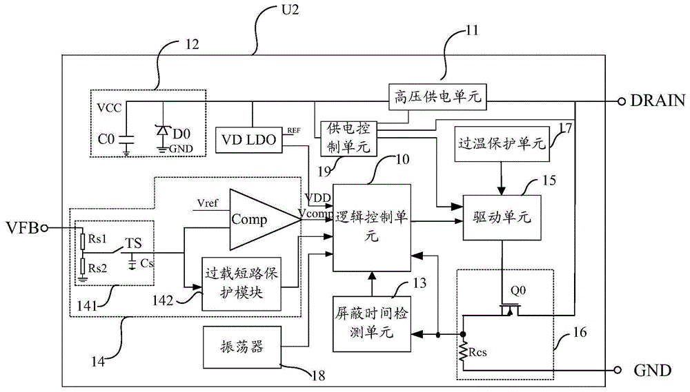
请参考图2至图4,本发明一实施例提供一种开关电源控制器U2,用于控制一开关电源系统的输出电压DC OUT。所述开关电源控制器U2包括:逻辑控制单元10、高压供电单元11、内置储能单元12、屏蔽时间检测单元13、电压检测单元14、驱动单元15、功率开关管采样单元16、过温保护单元17、振荡器18以及供电控制单元19。且这些单元集成在同一封装体(即芯片)内,使得本实施例的开关电源控制器为一开关电源控制芯片。振荡器(OSC)18与逻辑控制单元10电连接,用于调整开关电源系统的工作频率。Referring to FIGS. 2 to 4 , an embodiment of the present invention provides a switching power supply controller U2 for controlling the output voltage DC OUT of a switching power supply system. The switching power supply controller U2 includes: a
请参考图3,功率开关管采样单元16包括功率开关管Q0和采样电阻Rcs,功率开关管Q0的漏端连接开关电源系统的母线直流电压端DRAIN,源极连接采样电阻Rcs的一端,栅极连接驱动单元15,采样电阻Rcs的另一端接地。所述功采样电阻Rcs用于对流过所述功率开关管Q0的电流进行采样,以反映开关电源系统的负载变化。当然,在本发明的其他实施例中,所述采样电阻Rcs还可以被替代为MOS管或三极管等其他元器件。Please refer to FIG. 3 , the power switch
驱动单元15的一输入端连接逻辑控制单元10,另一输入端连接过温保护单元17,驱动单元15的输出端连接功率开关管Q0的栅极,驱动单元15用于在所述逻辑控制单元10的控制下驱动所述功率开关管Q0导通或关断,以调整所述开关电源系统的输出电压DC OUT。其中,功率开关管Q0关断后,图2中的电感L开始退磁过程。One input end of the
过温保护单元17用于检测开关电源控制器的芯片温度,并在所述芯片温度超过预设温度阈值时,能够控制驱动单元15来关断功率开关管Q0,以避免功率开关管Q0因温度过高而失效,同时减小开关电源控系统的输出功率,进而及时降低芯片温度。The
屏蔽时间检测单元13,又称为前沿消隐(leading edge blanking,LEB)单元,其输出端连接所述逻辑控制单元10,其输入端连接功率开关管Q0的源极,屏蔽时间检测单元13用于向所述逻辑控制单元10反馈所述功率开关管采样单元16电流采样的屏蔽时间,由此,逻辑控制单元10能根据屏蔽时间检测单元13的反馈结果,控制电压检测单元14对输出电压DC OUT进行周期性电压采样。The masking
电压检测单元14包括电压采样模块141、第二电子开关Ts、滤波电容Cs和比较器C0mp,第二电子开关Ts可以是MOS晶体管或三极管等电子元器件,电压采样模块141包括串联在所述输出电压反馈端VFB和地之间的两个电压采样电阻Rs1、Rs2。两个电压采样电阻Rs1、Rs2相互连接的节点为所述电压采样模块141的采样输出端,连接第二电子开关Ts的通路一端。采样电阻Rs1与输出电压反馈端VFB连接的一端为电压采样模块141的采样输入端。本实施例中,所述两个电压采样电阻Rs1、Rs2内置于所述开关电源控制器的芯片内部。第二电子开关Ts的通路另一端连接一滤波电容Cs和比较器C0mp的一输入端,第二电子开关Ts的控制端连接逻辑控制单元10的相应的信号输出端,比较器C0mp的另一输入端接入第二参考电压Vref,比较器C0mp的输出端连接所述逻辑控制单元10的输出补偿端VC0mp。第二电子开关Ts在逻辑控制单元10的控制下导通,以实现对输出电压DC OUT的电压采样,进而使得比较器C0mp能够比较电压采样得到的电压和第二参考电压Vref之间的大小,以输出电压补偿信号VC0mp,逻辑控制单元10能够根据VC0mp信号来产生控制驱动单元15的PWM(脉宽调制)信号或PFM(脉冲频率调制)信号,进而驱动单元15驱动所述功率开关管Q0导通或关断,以调整所述开关电源系统的输出电压DC OUT。电压检测单元14可以在退磁阶段(即功率开关管Q0关断后)实时反应输出电压DC OUT的值,从而实现逻辑控制单元10对输出电压的精确和快速控制。The
可选地,所述电压检测单元14还包括过载短路保护模块142,所述过载短路保护模块142的输入端连接所述第二电子开关Ts与所述比较器C0mp相互连接的一端,所述过载短路保护模块142的输出端连接所述逻辑控制单元10的相应的输入端。所述过载短路保护模块142用于在所述开关电源系统发生输出短路和/过载时,对流经所述功率开关管Q0和负载上的输出电流进行控制,以保护所述开关电源系统。过载短路保护模块142的电路设计可以参考本申请人之前的专利申请CN105870896A,在此不再赘述。Optionally, the
内置储能单元12用于在开关电源控制器的芯片启动和输出建立完成后,向所述逻辑控制单元10供电,以使得开关电源控制器U2能够维持正常工作状态等。本实施例,内置储能单元12中包括储能电容C0和稳压二极管D0,储能电容C0的一端和稳压二极管D0的阳极均接地,储能电容C0的另一端作为节点VCC,和稳压二极管D0的阴极相互连接,此时,节点VCC既作为内置储能单元12的电力输入端,又做为内置储能单元12的电力输出端。节点VCC还连接供电控制单元19的一输入端。其中稳压二极管D0能够控制节点VCC上的电压。在本发明的其他实施例中,如图4所示,可以省略稳压二极管D0,且在节点VCC和高压供电单元11之间连接第一线性稳压器HV LDO,该第一线性稳压器HV LDO,一方面起到稳压作用,以精确控制节点VCC上的电压,另一方面起到隔离作用,防止内置储能单元12的储能电容C0对功率开关管Q0的漏极Drain放电。The built-in
高压供电单元11的输入端连接所述开关电源系统的母线直流电压端DRAIN(即功率开关管Q0的漏端),高压供电单元11的一个输出端连接储能电容C0的另一端和稳压二极管D0的阴极,即连接节点VCC,高压供电单元11的另一个输出端连接供电控制单元19的另一输入端。供电控制单元19的又一输入端连接功率开关管的漏极,供电控制单元19的输出端连接驱动单元15的电源端。其中,高压供电单元11可以包括耗尽型场效应管,其具体电路设计可以参考本申请人之前的专利申请CN104124878A,在此不再赘述。供电控制单元19可以包括电流源、电压比较器,以及用于选通相应电流通路的选通开关(例如MOS管或触发器等),供电控制单元19中的电压比较器可以用于在功率开关管导通阶段判断功率开关管的漏极电压与一设定值之间的大小,以确定功率开关管的漏极电压是否被拉低,由此根据判断结果来选择高压供电单元17还是内置储能单元12来对驱动单元15供电。供电控制单元19中的电流源用于控制供电电流的大小,例如,可以在开关电源控制器U2的芯片启动和输出建立阶段,使得向驱动单元15供电的电流较小,而在开关电源控制器U2的芯片启动和输出建立后,使得向驱动单元15供电的电流比较大。The input terminal of the high-voltage power supply unit 11 is connected to the DC voltage terminal DRAIN of the busbar of the switching power supply system (ie, the drain terminal of the power switch tube Q0), and an output terminal of the high-voltage power supply unit 11 is connected to the other end of the energy storage capacitor C0 and the Zener diode. The cathode of D0 is connected to the node VCC, and the other output terminal of the high-voltage power supply unit 11 is connected to the other input terminal of the power
本实施例中,高压供电单元11的一个输出端直接连接节点VCC,能够在开关电源控制器U2的芯片启动和输出建立之前,向所述逻辑控制单元10供电并向储能电容C0充电。而节点VCC又通过第二线性稳压器VD LDO连接逻辑控制单元10的工作电压端VDD,因此在开关电源控制器U2的芯片启动和输出建立后(即开关电源控制器U2进入了正常工作阶段之后),内置储能单元12能够向逻辑控制单元10供电,进而使得逻辑控制单元10控制驱动单元15来驱动功率开关管Q0导通或关断。由于高压供电单元11的另一个输出端以及内置储能单元12的电力输出端均连接供电驱动单元19,因此,在功率开关管Q0刚导通阶段且功率开关管Q0的漏极电压未被拉低之前,可以通过供电控制单元19选择高压供电单元11直接向驱动单元15供电,在功率开关管Q0的漏极电压被拉低之后,功率开关管Q0进入完全导通阶段,此时可以通过供电控制单元19选择内置储能单元12直接向驱动单元15供电。由此,可以降低功率开关管Q0中的驱动电流损耗。In this embodiment, one output terminal of the high voltage power supply unit 11 is directly connected to the node VCC, which can supply power to the
在本发明的另一实施例中,在功率开关管Q0刚导通阶段且功率开关管Q0的漏极电压未被拉低之前,供电控制单元19也可以选择高压供电单元11和内置储能单元12同时向驱动单元15供电,以提高向驱动单元15的供电效率,且在功率开关管Q0的漏极电压被拉低之后,供电控制单元19选择内置储能单元12直接向驱动单元15供电。在本发明的又一实施例中,在内置储能单元12的储能容量满足要求的情况下,在功率开关管Q0的整个导通阶段,供电控制单元19均选择内置储能单元12向驱动单元15供电,由此可以简化供电控制策略。In another embodiment of the present invention, the power
可选地,所述开关电源控制器U2还包括第二线性稳压器VD LDO,第二线性稳压器VD LDO的一电压输入端连接节点VCC和供电控制单元19的公共端,第二线性稳压器VD LDO的电压输出端连接逻辑控制单元10的工作电压端VDD,第二线性稳压器VD LDO的另一电压输入端接入第一参考电压REF,所述第二线性稳压器VD LDO用于在储能电容C0向逻辑控制单元10供电时,根据所述第一参考电压REF,将所述储能电容C0所输出的电压VCC调整至所述逻辑控制单元10所需的工作电压VDD,以及,在所述高压供电单元11向逻辑控制单元10供电时,根据所述第一参考电压REF将所述高压供电单元11所输出的电压调整至所述逻辑控制单元10所需的工作电压VDD。Optionally, the switching power supply controller U2 further includes a second linear regulator VD LDO, a voltage input terminal of the second linear regulator VD LDO is connected to the node VCC and the common terminal of the power
请参考图2至图5,本发明一实施例还提供一种开关电源系统,包括:交流电压源ACIN、与所述交流电压源AC IN连接的整流电路、与所述整流电路连接的母线电容C1、与所述母线电容C1和所述整流电路的公共端连接的母线直流电压端DRAIN、本发明的开关电源控制器U2、电感L、二极管D5、D6以及输出电容C2。所述开关电源控制器U2接入在所述母线直流电压端DRAIN和所述开关电源系统的输出电压端DC OUT之间。整流电路包括四个二极管D1~D4。电感L一端接二极管D5的阴极和开关电源控制器U2的地端,另一端接输出电容C2的一端和二极管D6的阳极,输出电容C2的另一端和二极管D5的阳极均接地,二极管D6的阴极接开关电源控制器U2的输出电压反馈端VFB。交流电压源AC IN通过四个二极管D1~D4整流和母线电容C1滤波得到直流电压Vbus。功率开关管Q0、电感L、二极管D6以及输出电容C2组成典型的high-side buck开关电源拓扑。二极管D6可以隔离开关电源控制器U2启动阶段的高压,此时电压采样电阻Rs1和Rs2可以选用低压电阻。Referring to FIG. 2 to FIG. 5 , an embodiment of the present invention further provides a switching power supply system, including: an AC voltage source ACIN, a rectifier circuit connected to the AC voltage source AC IN, and a bus capacitor connected to the rectifier circuit C1, the bus DC voltage terminal DRAIN connected to the bus capacitor C1 and the common terminal of the rectifier circuit, the switching power supply controller U2 of the present invention, the inductor L, the diodes D5, D6 and the output capacitor C2. The switching power supply controller U2 is connected between the DC voltage terminal DRAIN of the busbar and the output voltage terminal DC OUT of the switching power supply system. The rectifier circuit includes four diodes D1-D4. One end of the inductor L is connected to the cathode of the diode D5 and the ground of the switching power supply controller U2, the other end is connected to one end of the output capacitor C2 and the anode of the diode D6, the other end of the output capacitor C2 and the anode of the diode D5 are both grounded, and the cathode of the diode D6 Connect to the output voltage feedback terminal VFB of the switching power supply controller U2. The AC voltage source AC IN is rectified by four diodes D1 to D4 and filtered by the bus capacitor C1 to obtain the DC voltage Vbus. Power switch tube Q0, inductor L, diode D6 and output capacitor C2 form a typical high-side buck switching power supply topology. The diode D6 can isolate the high voltage in the startup phase of the switching power supply controller U2. At this time, the voltage sampling resistors Rs1 and Rs2 can be selected as low voltage resistors.
作为一种示例,本实施例的开关电源系统为high side buck开关电源系统,开关电源系统的输出电压端DC OUT所输出的电压小于直流电压Vbus。As an example, the switching power supply system of this embodiment is a high side buck switching power supply system, and the voltage output by the output voltage terminal DC OUT of the switching power supply system is lower than the DC voltage Vbus.
在本发明的另一实施例中,请参考图2和图6,若电压采样电阻Rs1和Rs2使用高压电阻,可以省去输出电压反馈端VFB和输出电压端DC OUT之间的二极管D6,进一步精简外围电路。In another embodiment of the present invention, please refer to FIG. 2 and FIG. 6 , if the voltage sampling resistors Rs1 and Rs2 use high voltage resistors, the diode D6 between the output voltage feedback terminal VFB and the output voltage terminal DC OUT can be omitted, and further Simplify peripheral circuits.
在本发明的又一实施例中,请参考图2和图7,电压采样电阻Rs1和Rs2还可以外置于开关电源控制器U2的芯片外部,由此,即可以输出电压反馈端VFB和输出电压端DC OUT之间的二极管D6,也可以通过改变开关电源控制器U2的芯片外围的电压采样电阻Rs1和Rs2的阻值来改变输出电压DC OUT,应用更加灵活。In yet another embodiment of the present invention, please refer to FIG. 2 and FIG. 7 , the voltage sampling resistors Rs1 and Rs2 can also be placed outside the chip of the switching power supply controller U2, so that the voltage feedback terminal VFB and the output voltage can be output. The diode D6 between the voltage terminals DC OUT can also change the output voltage DC OUT by changing the resistance values of the voltage sampling resistors Rs1 and Rs2 on the periphery of the chip of the switching power supply controller U2, and the application is more flexible.
本发明一实施例还提供一种开关电源系统供电方法,适用于图2至图7所示的开关电源系统,所述开关电源系统供电方法包括:An embodiment of the present invention also provides a power supply method for a switching power supply system, which is suitable for the switching power supply system shown in FIG. 2 to FIG. 7 . The power supply method for the switching power supply system includes:
首先,在开关电源系统的开关电源控制器U2芯片启动和输出建立前,由高压供电单元11向所述开关电源控制器的内置储能单元12的储能电容C0充电,同时由高压供电单元11向所述开关电源控制器的逻辑控制单元10供电,以完成开关电源控制器启动和输出建立。具体地,开关电源系统启动时,储能电容C0上的电压(即节点VCC的电压)初始为0,开关电源系统通过高压供电单元11对储能电容C0充电,储能电容C0上的电压逐渐上升。当储能电容C0上的电压大于等于一工作电压阈值时,逻辑控制单元10控制所述高压供电单元11关断,系统启动完成,节点VCC电压可以快速升高到达开关电源控制器U2芯片内设的启动电压阈值,完成开关电源控制器启动和输出建立。First, before the switching power supply controller U2 chip of the switching power supply system is started and the output is established, the high-voltage power supply unit 11 charges the energy storage capacitor C0 of the built-in
接着,在所述开关电源控制器U2芯片输出建立后,开关电源控制器U2进入正常的工作阶段,此时由内置储能单元12的储能电容C0通过第二线性稳压器VD LDO向逻辑控制单元10供电,且输出电压DC OUT被开关电源控制器U2的电压检测单元14周期性采样,逻辑控制单元10根据电压检测单元14的采样结果来控制驱动单元15驱动功率开关管Q0导通或关断。Then, after the chip output of the switching power supply controller U2 is established, the switching power supply controller U2 enters the normal working stage, and the storage capacitor C0 of the built-in
此外,开关电源系统的系统消耗包括开关电源控制器U2的芯片工作电流消耗和驱动电流损耗,开关电源控制器U2的芯片工作电流消耗存在于功率开关管Q0的整个工作周期(包括导通阶段和关断阶段)中,而驱动电流损耗主要集中在功率开关管Q0的开启阶段(即刚导通阶段),功率开关管Q0中的驱动电流损耗和功率开关管Q0的寄生电容有很大关系。为了降低功率开关管Q0的驱动电流损耗,本实施例中,在功率开关管Q0关断阶段,由高压供电单元11对储能电容C0进行充电,使储能电容C0上的电压被预充到一预设值,该预设值小于等于储能电容C0的耐压值且尽量高;在功率开关管Q0刚导通阶段,功率开关管Q0的驱动电流可分为两部分提供,在功率开关管Q0的漏极电压未被拉低前,由供电控制单元19选择高压供电单元11向驱动单元15供电,以向功率开关管Q0提供相应的驱动电流,相当于功率开关管Q0的驱动电流直接由高压供电单元11提供,在功率开关管Q0的漏极电压被拉低后,功率开关管Q0进入了完全导通的阶段,此时由供电控制单元19选择储能电容C0向驱动单元15供电,以向功率开关管Q0提供相应的驱动电流,相当于功率开关管Q0的驱动电流直接由储能电容C0提供。且由于储能电容C0的电压在功率开关管Q0关断阶段被高压供电单元11预充到尽量高,因此在功率开关管Q0导通阶段,储能电容C0向所述驱动单元15供电的时间能被维持的尽量长。需要说明的是,储能电容C0向开关电源控制器U2的逻辑控制单元10供电的时间不小于功率开关管Q0的导通时间为Ton。In addition, the system consumption of the switching power supply system includes the chip working current consumption and driving current consumption of the switching power supply controller U2, and the chip working current consumption of the switching power supply controller U2 exists in the entire working cycle of the power switch Q0 (including the conduction phase and Turn-off stage), and the drive current loss is mainly concentrated in the turn-on stage of the power switch Q0 (ie, the just-on stage), and the drive current loss in the power switch Q0 has a great relationship with the parasitic capacitance of the power switch Q0. In order to reduce the driving current loss of the power switch Q0, in this embodiment, in the turn-off stage of the power switch Q0, the high-voltage power supply unit 11 charges the energy storage capacitor C0, so that the voltage on the energy storage capacitor C0 is precharged to A preset value, the preset value is less than or equal to the withstand voltage value of the energy storage capacitor C0 and is as high as possible; when the power switch transistor Q0 is just turned on, the driving current of the power switch transistor Q0 can be provided in two parts. Before the drain voltage of the transistor Q0 is pulled down, the power
通过这种供电方法,一方面减少了功率开关管的驱动电流损耗,因此节省了系统的总硬件消耗,另一方面改善了动态响应特性,并且提高了输出电压的精度。Through this power supply method, on the one hand, the driving current loss of the power switch tube is reduced, thus saving the total hardware consumption of the system, on the other hand, the dynamic response characteristic is improved, and the precision of the output voltage is improved.
在本发明的另一实施例中,在功率开关管Q0刚导通阶段,功率开关管Q0的驱动电流可分为两部分提供,在功率开关管Q0的漏极电压未被拉低前,由供电控制单元19选择高压供电单元11和内置储能单元12同时向驱动单元15供电,以向功率开关管Q0提供相应的驱动电流,相当于功率开关管Q0的驱动电流直接由高压供电单元11和内置储能单元12共同提供,在功率开关管Q0的漏极电压被拉低后,由供电控制单元19选择储能电容C0向驱动单元15供电,以向功率开关管Q0提供相应的驱动电流,相当于功率开关管Q0的驱动电流直接由储能电容C0提供。In another embodiment of the present invention, when the power switch Q0 is just turned on, the driving current of the power switch Q0 can be provided in two parts. Before the drain voltage of the power switch Q0 is pulled down, the driving current is The power
在本发明的又一实施例中,在功率开关管Q0的整个导通阶段,功率开关管Q0的驱动电流均有内置储能单元12来提供,具体地,在功率开关管Q0导通阶段,由供电控制单元19选择内置储能单元12同时向驱动单元15供电。In another embodiment of the present invention, in the entire conduction stage of the power switch Q0, the drive current of the power switch Q0 is provided by the built-in
在本发明的其他实施例中,在满足产品功耗要求的基础上,也可以省去供电控制单元19,并省去节点VCC向与驱动单元15的供电以及省去高压供电单元11向驱动单元15供电,由此使得驱动单元15的供电由逻辑控制单元10来提供,由此简化内部线路。In other embodiments of the present invention, on the basis of satisfying the power consumption requirements of the product, the power
需要说明的是,上述各实施例中,内置储能单元13中的储能元件均以电容为例,但是本发明的技术方案并不仅仅限定于此,内置储能单元13中的储能元件还可以被替换为电感或者电容和电感的组合等。It should be noted that, in the above embodiments, the energy storage elements in the built-in
另外,上述实施例中,虽然以“逻辑控制单元10、高压供电单元11、内置储能单元12、屏蔽时间检测单元13、电压检测单元14、驱动单元15和功率开关管采样单元16、过温保护单元17、振荡器18和供电控制单元19”集成在同一封装体(即芯片)内并单独作为一个模块为例来对本发明的开关电源控制器、开关电源系统以及开关电源系统供电方法进行了说明,但是本发明的技术方案并不仅仅限定于此。在本发明的其他实施例中,也可以是,逻辑控制单元10、高压供电单元11、内置储能单元12、屏蔽时间检测单元13、电压检测单元14、驱动单元15和功率开关管采样单元16、过温保护单元17、振荡器18、振荡器18和供电控制单元19中的至少一个单元的一部分结构或全部的结构和其他单元集成为一个功能模块。在本发明的其他实施例中,还可以是,逻辑控制单元10、高压供电单元11、内置储能单元12、屏蔽时间检测单元13、电压检测单元14、驱动单元15和功率开关管采样单元16、过温保护单元17、振荡器18和供电控制单元19中的至少一个单元的一部分结构或全部的结构外置于开关电源控制器的封装体(芯片)外,其余部分均集成在同一封装体(芯片)中,形成开关电源控制芯片。例如,仅电压检测单元14的电压采样模块141中的电压采样电阻Rs1、Rs2外置于开关电源控制器的封装体(芯片)之外,开关电源控制器的其余结构均集成在开关电源控制器的封装体(芯片)中。In addition, in the above embodiment, although the “
进一步需要说明的是,上述各实施例中,虽然均以内置储能单元12和高压供电单元11混合供电的方式为例进行的相应描述,但是本发明的技术方案并不仅仅限定于此。例如,在本发明的其他实施例中,例如负载均工作在CCM模式的high side buck开关电源系统中,其开关电源控制器可以设置有VCC外接端口或者Vin外接端口,在开关电源控制器的内部,可以将高压供电单元替换为一个高压电阻(未图示),且该高压电阻一端可以连接VCC外接端口或者Vin外接端口,以接入母线电压,另一端连接VD LDO,由此,开关电源控制器中能省略高压供电单元11,在开关电源控制器的芯片启动和输出建立阶段,由开关电源系统的母线电压Vbus向逻辑控制单元10供电并向内置储能单元13充电,之后的供电完全可以由内置储能单元13提供,由此简化开关电源控制器的结构,并降低开关电源控制器本身的芯片损耗,提高系统效率。It should be further noted that in the above embodiments, although the mixed power supply mode of the built-in
此外,本发明的技术方案不仅仅适用于high side buck开关电源系统,还适用于恒压输出的任意合适的开关电源系统,这些开关电源系统的输出电压能被电压检测单元周期性采样,逻辑控制单元能够根据采样结果来快速、精确地调整输出电压,由此改善了其动态响应特性,并且提高了输出电压的精度。In addition, the technical solution of the present invention is not only applicable to the high side buck switching power supply system, but also applicable to any suitable switching power supply system with constant voltage output. The output voltage of these switching power supply systems can be periodically sampled by the voltage detection unit and logically controlled The unit can quickly and accurately adjust the output voltage according to the sampling results, thereby improving its dynamic response characteristics and improving the accuracy of the output voltage.
上述描述仅是对本发明较佳实施例的描述,并非对本发明范围的任何限定,本发明领域的普通技术人员根据上述揭示内容做的任何变更、修饰,均属于权利要求书的保护范围。The above description is only a description of the preferred embodiments of the present invention, and is not intended to limit the scope of the present invention. Any changes and modifications made by those of ordinary skill in the field of the present invention based on the above disclosure all belong to the protection scope of the claims.
Claims (17)
Priority Applications (2)
| Application Number | Priority Date | Filing Date | Title |
|---|---|---|---|
| CN202010506987.XA CN111525822B (en) | 2020-06-05 | 2020-06-05 | Switching power supply controller, switching power supply system and switching power supply system power supply method |
| CN202110914239.XA CN113765418B (en) | 2020-06-05 | 2020-06-05 | Switching power supply controller, switching power supply system and switching power supply system power supply method |
Applications Claiming Priority (1)
| Application Number | Priority Date | Filing Date | Title |
|---|---|---|---|
| CN202010506987.XA CN111525822B (en) | 2020-06-05 | 2020-06-05 | Switching power supply controller, switching power supply system and switching power supply system power supply method |
Related Child Applications (1)
| Application Number | Title | Priority Date | Filing Date |
|---|---|---|---|
| CN202110914239.XA Division CN113765418B (en) | 2020-06-05 | 2020-06-05 | Switching power supply controller, switching power supply system and switching power supply system power supply method |
Publications (2)
| Publication Number | Publication Date |
|---|---|
| CN111525822A CN111525822A (en) | 2020-08-11 |
| CN111525822B true CN111525822B (en) | 2021-08-06 |
Family
ID=71911132
Family Applications (2)
| Application Number | Title | Priority Date | Filing Date |
|---|---|---|---|
| CN202010506987.XA Active CN111525822B (en) | 2020-06-05 | 2020-06-05 | Switching power supply controller, switching power supply system and switching power supply system power supply method |
| CN202110914239.XA Active CN113765418B (en) | 2020-06-05 | 2020-06-05 | Switching power supply controller, switching power supply system and switching power supply system power supply method |
Family Applications After (1)
| Application Number | Title | Priority Date | Filing Date |
|---|---|---|---|
| CN202110914239.XA Active CN113765418B (en) | 2020-06-05 | 2020-06-05 | Switching power supply controller, switching power supply system and switching power supply system power supply method |
Country Status (1)
| Country | Link |
|---|---|
| CN (2) | CN111525822B (en) |
Families Citing this family (1)
| Publication number | Priority date | Publication date | Assignee | Title |
|---|---|---|---|---|
| CN115378283B (en) * | 2022-07-28 | 2025-07-04 | 杭州士兰微电子股份有限公司 | Switching power supply controller, switching power supply and power supply method thereof |
Citations (1)
| Publication number | Priority date | Publication date | Assignee | Title |
|---|---|---|---|---|
| CN102263504A (en) * | 2010-05-26 | 2011-11-30 | 索尼公司 | Power supply circuit, integrated circuit device, solid-state imaging apparatus, and electronic apparatus |
Family Cites Families (7)
| Publication number | Priority date | Publication date | Assignee | Title |
|---|---|---|---|---|
| DE4111277A1 (en) * | 1991-04-08 | 1992-10-15 | Thomson Brandt Gmbh | STARTING CIRCUIT FOR A SWITCHING POWER SUPPLY |
| CN101562394B (en) * | 2009-03-06 | 2012-01-04 | 西安民展微电子有限公司 | Soft start circuit used in monolithic integration switching-type regulator |
| CN104485634B (en) * | 2014-12-16 | 2018-05-01 | 上海数明半导体有限公司 | Realize the power-supply management system and method for average current protection |
| CN106300962B (en) * | 2016-08-08 | 2019-06-11 | 杰华特微电子(杭州)有限公司 | A self-powered control circuit |
| CN107027218B (en) * | 2017-04-27 | 2018-09-21 | 深圳市芯飞凌半导体有限公司 | LED controls chip and LED light device |
| CN109478844B (en) * | 2017-06-02 | 2020-09-25 | 深圳市稳先微电子有限公司 | Power switch driving circuit with built-in power supply capacitor |
| CN108809101B (en) * | 2018-05-16 | 2021-03-23 | 深圳原能电器有限公司 | High-integration power management integrated circuit |
-
2020
- 2020-06-05 CN CN202010506987.XA patent/CN111525822B/en active Active
- 2020-06-05 CN CN202110914239.XA patent/CN113765418B/en active Active
Patent Citations (1)
| Publication number | Priority date | Publication date | Assignee | Title |
|---|---|---|---|---|
| CN102263504A (en) * | 2010-05-26 | 2011-11-30 | 索尼公司 | Power supply circuit, integrated circuit device, solid-state imaging apparatus, and electronic apparatus |
Also Published As
| Publication number | Publication date |
|---|---|
| CN113765418A (en) | 2021-12-07 |
| CN113765418B (en) | 2023-08-11 |
| CN111525822A (en) | 2020-08-11 |
Similar Documents
| Publication | Publication Date | Title |
|---|---|---|
| US11463012B1 (en) | Architecture for multi-port AC/DC switching mode power supply | |
| US11837957B2 (en) | Auxiliary voltage conversion unit for supplying power to a power adapter control circuit | |
| US9263956B2 (en) | Switch-mode power supply control apparatus and flyback switch-mode power supply including the control apparatus | |
| US9331583B2 (en) | Switch mode power supply, control circuit and associated control method | |
| CN111555643B (en) | Switching power supply controller, switching power supply system and switching power supply system power supply method | |
| JP4481879B2 (en) | Switching power supply | |
| US20130188401A1 (en) | Capacitor discharging circuit and converter | |
| US10651759B2 (en) | Switching power supply device and semiconductor device | |
| US10756636B2 (en) | Power control device switchable between multiple operating modes having different power consumption | |
| CN109660131B (en) | Switching power supply circuit, power supply method and switching power supply system | |
| CN114070105A (en) | Forward excitation constant current control device, switching power supply, control method and chip | |
| CN112653324B (en) | Boost converter system without direct power supply | |
| CN111342667B (en) | Power supply control method based on flyback converter and power supply circuit | |
| CN111525822B (en) | Switching power supply controller, switching power supply system and switching power supply system power supply method | |
| CN114649932A (en) | X capacitor control and start multiplexing circuit, switching power supply controller and switching power supply | |
| CN115378283B (en) | Switching power supply controller, switching power supply and power supply method thereof | |
| CN108390557B (en) | Improve the Switching Power Supply of underloading frequency | |
| US20250070641A1 (en) | Power conversion circuit and method | |
| CN209642550U (en) | A kind of Switching Power Supply power supply circuit and switch power supply system | |
| CN217522740U (en) | Direct current voltage regulating circuit, circuit board and electrical apparatus | |
| CN221509413U (en) | High-integration-level high-voltage non-isolated buck converter of automobile | |
| CN219394688U (en) | Starting circuit of control chip and switching power supply | |
| Chen et al. | Research on Single Chip Switching DC-DC Switching Power Supply | |
| US12294301B2 (en) | Power supply circuit and light-emitting diode (LED) driving system using power supply circuit | |
| US20250279713A1 (en) | Voltage holding circuit, voltage holding method, power circuit and electronic device |
Legal Events
| Date | Code | Title | Description |
|---|---|---|---|
| PB01 | Publication | ||
| PB01 | Publication | ||
| SE01 | Entry into force of request for substantive examination | ||
| SE01 | Entry into force of request for substantive examination | ||
| GR01 | Patent grant | ||
| GR01 | Patent grant | ||
| IP01 | Partial invalidation of patent right |
Commission number: 4W117147 Conclusion of examination: Maintain the validity of the patent based on claims 1-13 submitted by the patentee on February 21, 2024 Decision date of declaring invalidation: 20240705 Decision number of declaring invalidation: 569049 Denomination of invention: Switching power supply controller, switching power supply system, and power supply method for switching power supply system Granted publication date: 20210806 Patentee: SHANGHAI BRIGHT POWER SEMICONDUCTOR Co.,Ltd. |
|
| IP01 | Partial invalidation of patent right |