CN111474219A - Method for manufacturing working electrode of electrochemical sensor and product thereof - Google Patents
Method for manufacturing working electrode of electrochemical sensor and product thereof Download PDFInfo
- Publication number
- CN111474219A CN111474219A CN201910900637.9A CN201910900637A CN111474219A CN 111474219 A CN111474219 A CN 111474219A CN 201910900637 A CN201910900637 A CN 201910900637A CN 111474219 A CN111474219 A CN 111474219A
- Authority
- CN
- China
- Prior art keywords
- substrate
- grooves
- conductive
- working electrode
- conductive layer
- Prior art date
- Legal status (The legal status is an assumption and is not a legal conclusion. Google has not performed a legal analysis and makes no representation as to the accuracy of the status listed.)
- Withdrawn
Links
Images


Classifications
-
- G—PHYSICS
- G01—MEASURING; TESTING
- G01N—INVESTIGATING OR ANALYSING MATERIALS BY DETERMINING THEIR CHEMICAL OR PHYSICAL PROPERTIES
- G01N27/00—Investigating or analysing materials by the use of electric, electrochemical, or magnetic means
- G01N27/26—Investigating or analysing materials by the use of electric, electrochemical, or magnetic means by investigating electrochemical variables; by using electrolysis or electrophoresis
- G01N27/28—Electrolytic cell components
- G01N27/30—Electrodes, e.g. test electrodes; Half-cells
- G01N27/327—Biochemical electrodes, e.g. electrical or mechanical details for in vitro measurements
- G01N27/3271—Amperometric enzyme electrodes for analytes in body fluids, e.g. glucose in blood
- G01N27/3272—Test elements therefor, i.e. disposable laminated substrates with electrodes, reagent and channels
-
- G—PHYSICS
- G01—MEASURING; TESTING
- G01N—INVESTIGATING OR ANALYSING MATERIALS BY DETERMINING THEIR CHEMICAL OR PHYSICAL PROPERTIES
- G01N27/00—Investigating or analysing materials by the use of electric, electrochemical, or magnetic means
- G01N27/26—Investigating or analysing materials by the use of electric, electrochemical, or magnetic means by investigating electrochemical variables; by using electrolysis or electrophoresis
- G01N27/28—Electrolytic cell components
- G01N27/30—Electrodes, e.g. test electrodes; Half-cells
- G01N27/307—Disposable laminated or multilayered electrodes
-
- G—PHYSICS
- G01—MEASURING; TESTING
- G01N—INVESTIGATING OR ANALYSING MATERIALS BY DETERMINING THEIR CHEMICAL OR PHYSICAL PROPERTIES
- G01N27/00—Investigating or analysing materials by the use of electric, electrochemical, or magnetic means
- G01N27/26—Investigating or analysing materials by the use of electric, electrochemical, or magnetic means by investigating electrochemical variables; by using electrolysis or electrophoresis
- G01N27/28—Electrolytic cell components
- G01N27/30—Electrodes, e.g. test electrodes; Half-cells
- G01N27/302—Electrodes, e.g. test electrodes; Half-cells pH sensitive, e.g. quinhydron, antimony or hydrogen electrodes
-
- G—PHYSICS
- G01—MEASURING; TESTING
- G01N—INVESTIGATING OR ANALYSING MATERIALS BY DETERMINING THEIR CHEMICAL OR PHYSICAL PROPERTIES
- G01N27/00—Investigating or analysing materials by the use of electric, electrochemical, or magnetic means
- G01N27/26—Investigating or analysing materials by the use of electric, electrochemical, or magnetic means by investigating electrochemical variables; by using electrolysis or electrophoresis
- G01N27/28—Electrolytic cell components
- G01N27/30—Electrodes, e.g. test electrodes; Half-cells
- G01N27/327—Biochemical electrodes, e.g. electrical or mechanical details for in vitro measurements
-
- A—HUMAN NECESSITIES
- A61—MEDICAL OR VETERINARY SCIENCE; HYGIENE
- A61B—DIAGNOSIS; SURGERY; IDENTIFICATION
- A61B5/00—Measuring for diagnostic purposes; Identification of persons
- A61B5/145—Measuring characteristics of blood in vivo, e.g. gas concentration or pH-value ; Measuring characteristics of body fluids or tissues, e.g. interstitial fluid or cerebral tissue
- A61B5/1468—Measuring characteristics of blood in vivo, e.g. gas concentration or pH-value ; Measuring characteristics of body fluids or tissues, e.g. interstitial fluid or cerebral tissue using chemical or electrochemical methods, e.g. by polarographic means
- A61B5/1486—Measuring characteristics of blood in vivo, e.g. gas concentration or pH-value ; Measuring characteristics of body fluids or tissues, e.g. interstitial fluid or cerebral tissue using chemical or electrochemical methods, e.g. by polarographic means using enzyme electrodes, e.g. with immobilised oxidase
Landscapes
- Life Sciences & Earth Sciences (AREA)
- Health & Medical Sciences (AREA)
- Chemical & Material Sciences (AREA)
- Biochemistry (AREA)
- General Physics & Mathematics (AREA)
- Electrochemistry (AREA)
- Physics & Mathematics (AREA)
- Analytical Chemistry (AREA)
- Molecular Biology (AREA)
- General Health & Medical Sciences (AREA)
- Chemical Kinetics & Catalysis (AREA)
- Immunology (AREA)
- Pathology (AREA)
- Biophysics (AREA)
- Hematology (AREA)
- Investigating Or Analyzing Materials By The Use Of Electric Means (AREA)
- Measuring Oxygen Concentration In Cells (AREA)
- Investigating Or Analyzing Materials By The Use Of Fluid Adsorption Or Reactions (AREA)
Abstract
本发明公开了一种电化学传感器的工作电极制作方法以及一种电化学传感器的工作电极,该电化学传感器的工作电极制作方法包含以下步骤:步骤S1,提供一基板;步骤S2,设置一波浪图案,将该波浪图案形成于该基板的一面;以及步骤S3,提供一导电物质,将该导电物质设于该基板具有该波浪图案的一面。
The invention discloses a method for making a working electrode of an electrochemical sensor and a working electrode of an electrochemical sensor. The method of making a working electrode of an electrochemical sensor includes the following steps: step S1, providing a substrate; step S2, setting a wave pattern, forming the wavy pattern on one side of the substrate; and step S3, providing a conductive material, and disposing the conductive material on the side of the substrate having the wavy pattern.
Description
技术领域technical field
一种电化学传感器的工作电极制作方法及其产品,尤指一种提升现有制作电化学三电极感测制作精度方法及其产品。The invention relates to a method for manufacturing a working electrode of an electrochemical sensor and a product thereof, in particular a method and a product for improving the manufacturing accuracy of the existing electrochemical three-electrode sensing.
背景技术Background technique
近年各种医疗用检测装置的普及率越来越高,并且可于病床边或诊间进行快速检测方式越来越受到重视。这样的快速检测方式不仅需要具备高灵敏性与高选择性的检测特性,还必须是小型、便宜且易于操作。In recent years, the popularity of various medical testing devices has been increasing, and rapid testing methods that can be performed at the bedside or in the clinic have received more and more attention. Such a rapid detection method not only needs to have the detection characteristics of high sensitivity and high selectivity, but also must be small, cheap and easy to operate.
而最为常见的例子就是血糖仪,目前市售的血糖仪大都使用三电极抛弃式试片,三电极抛弃式试片由网版印刷技术所制作。但网印的制程精度,无法达到日趋严苛测量准确度的需求。The most common example is a blood glucose meter. Currently, most of the commercially available blood glucose meters use a three-electrode disposable test piece, which is made by screen printing technology. However, the process accuracy of screen printing cannot meet the increasingly stringent measurement accuracy requirements.
发明内容SUMMARY OF THE INVENTION
有鉴于此,本发明主要目的在于,提出一种电化学传感器的工作电极制作方法及其产品,其提升现有制作电化学三电极感测制作精度方法及其产品。工作电极的表面具有波浪图案,以增加感测面积。本发明可于工作电极固定接合酵素、抗体或核酸,以应用于不同领域的生物感测。In view of this, the main purpose of the present invention is to provide a method for manufacturing a working electrode of an electrochemical sensor and a product thereof, which improve the manufacturing accuracy of the existing method for manufacturing electrochemical three-electrode sensing and the product thereof. The surface of the working electrode has a wave pattern to increase the sensing area. The present invention can immobilize and bind enzymes, antibodies or nucleic acids to the working electrodes, so as to be applied to biological sensing in different fields.
为达上述目的,本发明所提出的一种电化学传感器的工作电极制作方法,其包含以下步骤:In order to achieve the above purpose, a method for making a working electrode of an electrochemical sensor proposed by the present invention comprises the following steps:
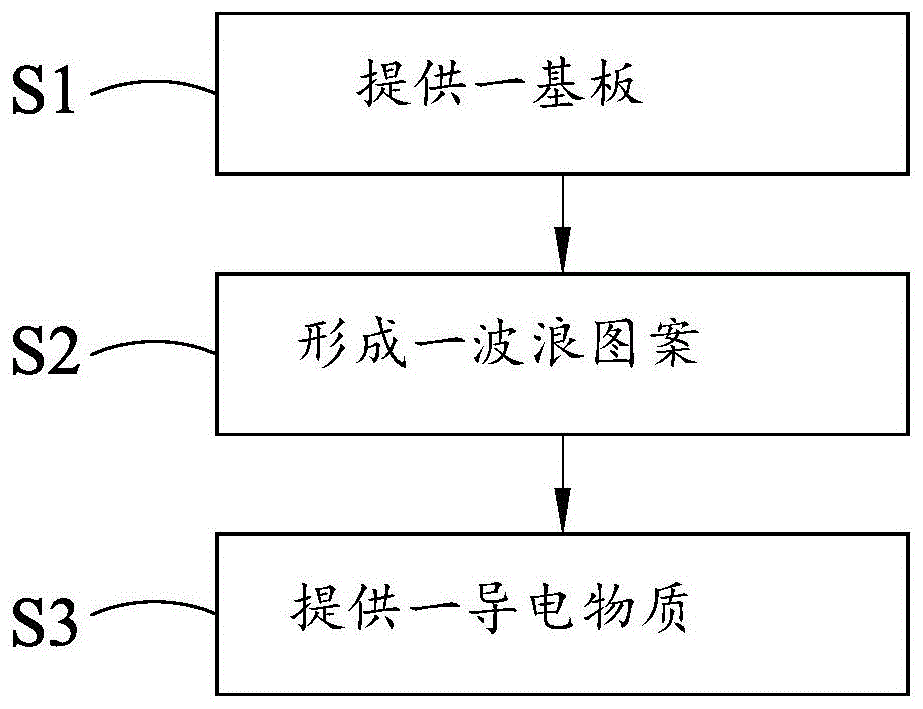
步骤S1,提供一基板;Step S1, providing a substrate;
步骤S2,设置一波浪图案,将该波浪图案形成于该基板的一面;以及Step S2, setting a wave pattern, and forming the wave pattern on one side of the substrate; and
步骤S3,提供一导电物质,将该导电物质设于该基板具有该波浪图案的一面。In step S3, a conductive substance is provided, and the conductive substance is disposed on the side of the substrate with the wave pattern.
于一实施例,该基板的一面具有一保护层。In one embodiment, one side of the substrate has a protective layer.
于一实施例,于该步骤S1中,对该基板具有该保护层的一面进行黄光与干式蚀刻,而使该面形成有多个开孔。In one embodiment, in the step S1, yellow light and dry etching are performed on the surface of the substrate with the protective layer, so that a plurality of openings are formed on the surface.
于一实施例,于该步骤S1中,对该基板具有该多个开孔的位置进行等相蚀刻,以使具有该多个开孔位置的该基板形成有多个凹槽,该多个凹槽为半圆形;或者对该基板具有该多个开孔的位置进行非等相蚀刻,以使具有该多个开孔位置的该基板形成有多个凹槽,该多个凹槽为倒三角形,该多个凹槽的边缘与底缘处具有至少一尖角。In one embodiment, in the step S1, isophase etching is performed on the positions of the substrate with the plurality of openings, so that the substrate with the plurality of openings is formed with a plurality of grooves, and the plurality of grooves are formed. The grooves are semi-circular; or the positions of the substrate with the plurality of openings are etched anisoly, so that the substrate with the plurality of opening positions is formed with a plurality of grooves, and the plurality of grooves are inverted In a triangle shape, the edges and bottom edges of the plurality of grooves have at least one sharp corner.
于一实施例,于该步骤S1中,将该基板的该保护层于以去除;将该基板浸泡于上述的等相时刻液体中,待浸泡数秒后,以该使该多个凹槽与该基板的表面的尖角,形成导圆角,或者将该基板浸泡于上述的等相时刻液体中,待浸泡数秒后,以使呈三角形的该多个凹槽与该多个尖角,形成导圆角;或者将该基板处以热氧化,而使该多个凹槽具有导圆角,以及该多个尖角形成导圆角;该多个导圆角的凹槽构成该波浪图案。In one embodiment, in the step S1, the protective layer of the substrate is removed; the substrate is immersed in the above-mentioned isophase liquid, and after soaking for several seconds, the plurality of grooves and the The sharp corners of the surface of the substrate form rounded corners, or the substrate is immersed in the above-mentioned isophase liquid, and after soaking for several seconds, the plurality of triangular grooves and the plurality of sharp corners form lead corners. or the substrate is thermally oxidized, so that the plurality of grooves have rounded corners, and the plurality of sharp corners form rounded corners; the plurality of rounded grooves form the wave pattern.
于一实施例,于该步骤S3中,以一物理气相沉积对该基板具有该波浪图案的一面进行蒸镀或溅镀,而使该面沉积有一导电层。一胶体金属溶液具有导电颗粒与胶体溶液,将该胶体金属溶液设于该基板具有该导电层的一面;待该胶体溶液干燥后,该多个导电颗粒设于该导电层的一面。In one embodiment, in the step S3, vapor deposition or sputtering is performed on the side of the substrate having the wave pattern by a physical vapor deposition, so that a conductive layer is deposited on the side. A colloidal metal solution has conductive particles and a colloidal solution, and the colloidal metal solution is disposed on the side of the substrate with the conductive layer; after the colloidal solution is dried, the conductive particles are disposed on one side of the conductive layer.
本发明复提出一种电化学传感器的工作电极,其包含有:The present invention further proposes a working electrode of an electrochemical sensor, which comprises:
一基板;a substrate;
一波浪图案,其设于该基板的一面;以及a wave pattern provided on one side of the substrate; and
一导电物质,其设于该基板具有该波浪图案的一面。A conductive substance is arranged on the side of the substrate with the wave pattern.
于一实施例,该波浪图案为该基板的多个凹槽,各凹槽的边缘与底缘处具有圆角。In one embodiment, the wave pattern is a plurality of grooves of the substrate, and the edge and bottom edge of each groove have rounded corners.
于一实施例,该导电物质具有一导电层,该导电层位于该基板具有该多个凹槽的一面;或者,该导电物质具有一导电层与多个导电颗粒,该导电层位于该基板具有该多个凹槽的一面,该多个导电颗粒位于该导电层远离该基板的一面。In one embodiment, the conductive material has a conductive layer, and the conductive layer is located on the side of the substrate with the plurality of grooves; or, the conductive material has a conductive layer and a plurality of conductive particles, and the conductive layer is located on the substrate with On one side of the plurality of grooves, the plurality of conductive particles are located on the side of the conductive layer away from the substrate.
综合上述,本发明的电化学传感器的工作电极制作方法及其产品,其将要求高精度及使用金属,设置纳米金属颗粒的工作电极制作为芯片,芯片的感测区表面具有波浪图案,波浪图案增加感应的表面积,以提高测量的精准度。本发明的工作电极可黏贴于现有低成本制作的抛弃式式片,藉此兼顾及成本的竞争优势。To sum up the above, the method for making a working electrode of an electrochemical sensor and the product thereof of the present invention require high precision and use metal, and the working electrode provided with nano metal particles is made into a chip, and the surface of the sensing area of the chip has a wave pattern, and the wave pattern Increase the sensing surface area to improve measurement accuracy. The working electrode of the present invention can be pasted on the existing low-cost disposable sheet, thereby taking into account the competitive advantage of cost.
附图说明Description of drawings
图1为本发明的电化学传感器的工作电极制作方法的流程图。FIG. 1 is a flow chart of a method for fabricating a working electrode of an electrochemical sensor of the present invention.
图2为一具有开孔的基板的第一实施例的示意图。FIG. 2 is a schematic diagram of a first embodiment of a substrate with openings.
图3为一具有凹层的基板的第一实施例的示意图。3 is a schematic diagram of a first embodiment of a substrate having a recessed layer.
图4为一基板的第一实施例的示意图。FIG. 4 is a schematic diagram of a first embodiment of a substrate.
图5为一具有波浪图案的第一实施例的基板的示意图。FIG. 5 is a schematic diagram of a substrate having a wave pattern according to the first embodiment.
图6为一具有导电层的第一实施例的基板的示意图。FIG. 6 is a schematic diagram of a substrate having a conductive layer according to a first embodiment.
图7为一具有导电物质的第二实施例的基板的示意图。FIG. 7 is a schematic diagram of a substrate having a second embodiment of a conductive substance.
图8为一具有开孔的基板的第三实施例的示意图。FIG. 8 is a schematic diagram of a third embodiment of a substrate with openings.
图9为一具有凹层的基板的第三实施例的示意图。9 is a schematic diagram of a third embodiment of a substrate having a recessed layer.
图10为一基板的第三实施例的示意图。FIG. 10 is a schematic diagram of a third embodiment of a substrate.
图11为一具有波浪图案的第三实施例的基板的示意图。FIG. 11 is a schematic diagram of a substrate having a third embodiment of a wave pattern.
图12为一具有导电层的第三实施例的基板的示意图。FIG. 12 is a schematic diagram of a third embodiment of a substrate having a conductive layer.
图13为一具有导电物质的第三实施例的基板的示意图。FIG. 13 is a schematic diagram of a substrate having a third embodiment of a conductive substance.
附图标记说明:10-基板;100-凹槽;101-尖角;102-导圆角;103-波浪图案;11-保护层;110-开孔;12-导电层;13-导电颗粒;20-基板;200-凹槽;201-尖角;202-导圆角;203-凹槽;204-波浪图案;21-保护层;210-开孔;22-导电层;23-导电颗粒;S1~S3-步骤。Description of reference numerals: 10-substrate; 100-groove; 101-sharp corner; 102-rounding corner; 103-wave pattern; 11-protective layer; 110-opening hole; 12-conductive layer; 13-conductive particle; 20-substrate; 200-groove; 201-sharp corner; 202-rounded corner; 203-groove; 204-wave pattern; 21-protective layer; 210-hole; 22-conductive layer; 23-conductive particle; S1~S3-steps.
具体实施方式Detailed ways
请配合参考图1所示,本发明为一种电化学传感器的工作电极制作方法的第一实施例,其步骤包含有:Please refer to FIG. 1 , the present invention is a first embodiment of a method for fabricating a working electrode of an electrochemical sensor. The steps include:
步骤S1,提供一基板。请配合参考图2所示,一基板10的一面具有一保护层11。该基板10为氧化物(Oxide)/氮化物(Nitride)晶圆。该基板10为1至100欧姆-公分(ohm-cm)的硅晶圆。Step S1, providing a substrate. Please refer to FIG. 2 , one side of a
步骤S2,形成一波浪图案。请再参阅图2所示,对基板10具有保护层11的一面进行黄光与干式蚀刻,而使该面形成有多个开孔110。Step S2, forming a wave pattern. Referring to FIG. 2 again, yellow light and dry etching are performed on the surface of the
请配合参考图3所示,对基板10具有开孔110的位置进行等相蚀刻,以使具有开孔110位置的基板10形成有多个凹槽100,该多个凹槽100为半圆形凹槽。等向蚀刻液体为0.5~1.5单位的44至54%氟化氢(化学式:HF)与2.5~3.5单位65至75%硝酸(分子式:HNO3),蚀刻温度20至30℃。较佳为1单位的49%氟化氢与3单位70%硝酸,蚀刻温度25℃。Please refer to FIG. 3 , perform isophase etching on the positions of the
请配合参考图4与图5所示,待上述的凹槽100形成后,移除保护层11,该多个凹槽101的边缘与基板10的表面具有尖角101。再将基板10浸泡于上述的等相时刻液体中,待浸泡数秒后,以使尖角101,形成导圆角102。或者以将基板10处以热氧化(Thermal Oxide),从而使前述的尖角101,形成导圆角102。该多个具有导圆角102的凹槽100构成一波浪图案103。Please refer to FIG. 4 and FIG. 5 together. After the above-mentioned
步骤S3,提供一导电物质,请配合参考图6所示,以一物理气相沉积(Physicalvapor deposition,PVD)对基板10具有波浪图案101的一面进行蒸镀或溅镀,而使该面沉积有一导电层12。举例而言,导电层12为铬-铜(Cr-Au)层。Step S3 , providing a conductive material, please refer to FIG. 6 , perform vapor deposition or sputtering on the side of the
请配合参考图1与图7所示,本发明为一种电化学传感器的工作电极制作方法的第二实施例,其步骤如上述的第一实施例,故元件符号沿用上述的第一实施例。Please refer to FIG. 1 and FIG. 7 together. The present invention is a second embodiment of a method for fabricating a working electrode of an electrochemical sensor. The steps are the same as those of the first embodiment. Therefore, the symbols of the components are the same as those of the first embodiment. .
于本实施例中,将一胶体金属溶液设于基板10具有导电层12的一面。待胶体溶液干燥后,导电颗粒13设于导电层12的一面。In this embodiment, a colloidal metal solution is disposed on the side of the
该胶体金属溶液将四氯金酸以柠檬酸化学还原法制备。导电颗粒13可为纳米金属颗粒,尺寸为1至100纳米(nano,nm)。若纳米金属颗粒为纳米金颗粒,则其方程式为:HAuCl4+Na3C6H5O7→nano Au。The colloidal metal solution is prepared by chemical reduction of tetrachloroauric acid with citric acid. The
请再配合参考图1所示,本发明为一种电化学传感器的工作电极制作方法的第一实施例,其步骤包含有:Please refer to FIG. 1 again. The present invention is a first embodiment of a method for fabricating a working electrode of an electrochemical sensor. The steps include:
步骤S1,提供一基板。请配合参考图8所示,一基板20的一面具有一保护层2。该基板20为氧化物(Oxide)/氮化物(Nitride)晶圆。该基板10为1至100欧姆-公分(ohm-cm)的硅晶圆。Step S1, providing a substrate. Please refer to FIG. 8 , one side of a
步骤S2,制作波浪图案。请再参阅图8所示,对基板20具有保护层21的一面进行黄光与干式蚀刻,而使该面形成有多个开孔210。Step S2, making a wave pattern. Referring to FIG. 8 again, yellow light and dry etching are performed on the side of the
请配合参考图9所示,对基板20具有开孔210的位置进行非等相蚀刻,以使具有开孔210位置的基板20形成有多个凹槽200,该多个凹槽200为倒三角形。该非等相蚀刻液为10至45%氢氧化钾(化学式:KOH),温度40至90℃;或者5至25%四甲基氢氧化铵(化学式:TMAH或TMAOH),温度40至90℃。Please refer to FIG. 9 , perform anisotropic etching on the positions of the
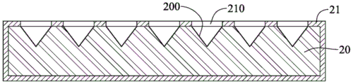
请配合参考图10所示,将基板20的保护层21于以去除。基板20的一面具有多个倒三角形的凹槽200。各凹槽200的边缘与底缘处具有至少一尖角201。Please refer to FIG. 10 to remove the
请再配合参考图10所示,待上述的凹槽200形成后,移除保护层21。请配合参考图11所示,再将基板20浸泡于上述的等相时刻液体中,待浸泡数秒后,以使呈三角形的凹槽200与尖角201,形成导圆角202。或者以将基板20处以热氧化(Thermal Oxide),而使前述的尖角201形成导圆角202,以及呈三角形的凹槽200形成为呈半圆形的凹槽203,。该多个导圆角的凹槽203构成一波浪图案204。Please refer to FIG. 10 again. After the above-mentioned
步骤S3,提供导电物质,请配合参考图12所示,以物理气相沉积对基板20具有波浪图案204的一面进行蒸镀或溅镀,而使该面沉积有一导电层22。举例而言,导电层22为铬-铜层。In step S3, a conductive material is provided, and as shown in FIG. 12, vapor deposition or sputtering is performed on the surface of the
请配合参考图13所示,将一胶体金属溶液设于基板20具有导电层22的一面。待胶体溶液干燥后,导电颗粒23设于导电层22的一面。Please refer to FIG. 13 , a colloidal metal solution is placed on the side of the
请配合参考图6所示,本发明为一种电化学传感器的工作电极的第一实施例,其包含有一基板10、一波浪图案101与一导电物质14。Please refer to FIG. 6 , the present invention is a first embodiment of a working electrode of an electrochemical sensor, which includes a
波浪图案101位于基板10的一面。于基板10具有多个凹槽100,各凹槽100的边缘与底缘处具有圆角102。该多个凹槽100形成波浪图案101。The
导电物质14设于基板10具有波浪图案101的一面,导电物质14为一导电层12。导电层12设于基板10具有波浪图案101的一面。The conductive substance 14 is disposed on the side of the
请配合参考图7所示,本发明为一种电化学传感器的工作电极的第一实施例,其包含有一基板10、一波浪图案101与一导电物质14。本实施例如上述的电化学传感器的工作电极的第一实施例,故元件符号沿用上述的电化学传感器的工作电极的第一实施例。Please refer to FIG. 7 , the present invention is a first embodiment of a working electrode of an electrochemical sensor, which includes a
于本实施例中。导电物质14为一导电层12与多个导电颗粒13。导电层12设于基板10具有波浪图案101的一面。导电颗粒13设于导电层12远离基板10的一面。in this example. The conductive substance 14 is a
综合上述,本发明的电化学传感器的工作电极制作方法及其产品,其是将要求高精度及使用金属,设置纳米金属颗粒的工作电极制作为芯片,芯片的感测区表面具有波浪图案,波浪图案增加感应的表面积,以提高测量的精准度。To sum up the above, the method for making a working electrode of an electrochemical sensor and the product thereof of the present invention are to make a working electrode that requires high precision and uses metal and is provided with nano metal particles as a chip, and the surface of the sensing area of the chip has a wave pattern, and the wave The pattern increases the sensing surface area to improve the accuracy of the measurement.
Claims (10)
Applications Claiming Priority (2)
| Application Number | Priority Date | Filing Date | Title |
|---|---|---|---|
| TW108102558 | 2019-01-23 | ||
| TW108102558A TWI675201B (en) | 2019-01-23 | 2019-01-23 | Working electrode of electrochemical sensor manufacturing method and product thereof |
Publications (1)
| Publication Number | Publication Date |
|---|---|
| CN111474219A true CN111474219A (en) | 2020-07-31 |
Family
ID=69023823
Family Applications (1)
| Application Number | Title | Priority Date | Filing Date |
|---|---|---|---|
| CN201910900637.9A Withdrawn CN111474219A (en) | 2019-01-23 | 2019-09-23 | Method for manufacturing working electrode of electrochemical sensor and product thereof |
Country Status (4)
| Country | Link |
|---|---|
| US (1) | US20200232941A1 (en) |
| EP (1) | EP3686584A1 (en) |
| CN (1) | CN111474219A (en) |
| TW (1) | TWI675201B (en) |
Citations (12)
| Publication number | Priority date | Publication date | Assignee | Title |
|---|---|---|---|---|
| US4851105A (en) * | 1987-02-16 | 1989-07-25 | Ngk Insulators, Ltd. | Oxygen sensing element and method for producing the same |
| JPH02216046A (en) * | 1989-02-15 | 1990-08-28 | Matsushita Electric Works Ltd | Electrochemical type sensor |
| US5685969A (en) * | 1993-09-28 | 1997-11-11 | Siemens Aktiengesellschaft | Sensor arrangement |
| JP2000097899A (en) * | 1998-09-24 | 2000-04-07 | エヌ・ティ・ティ・アドバンステクノロジ株式会社 | Micro online biosensor and production method thereof |
| US20010047941A1 (en) * | 2000-04-13 | 2001-12-06 | Masao Washizu | Electrode for dielectrophoretic apparatus, dielectrophoretic apparatus, method for manufacturing the same, and method for separating substances using the electrode or dielectrophoretic apparatus |
| JP2003075459A (en) * | 2001-09-03 | 2003-03-12 | Japan Science & Technology Corp | Method of forming electrodes on substrate having micro three-dimensional structure and microchip manufactured using the method |
| US20090008247A1 (en) * | 2007-07-05 | 2009-01-08 | Apex Biotechnology Corp. | Composite Modified Electrode Strip |
| US20090229857A1 (en) * | 2005-11-18 | 2009-09-17 | Replisaurus Technologies Ab | Electrode and method of forming the electrode |
| US20090321257A1 (en) * | 2008-06-24 | 2009-12-31 | Yoshifumi Takahara | Biosensor, method of producing the same and detection system comprising the same |
| CN102243207A (en) * | 2011-04-19 | 2011-11-16 | 复旦大学 | Electrochemical sensor with nanometer concave-convex structure formed on surface of electrode and preparation method of electrochemical sensor |
| KR20160063900A (en) * | 2014-11-27 | 2016-06-07 | 아이오틴 주식회사 | Sensor for Measuring blood glucose and Manufacturing Methods thereof |
| US20170219511A1 (en) * | 2016-01-29 | 2017-08-03 | National Chung Hsing University | Enzyme-free glucose detection chip |
Family Cites Families (2)
| Publication number | Priority date | Publication date | Assignee | Title |
|---|---|---|---|---|
| JP4434997B2 (en) * | 2005-03-08 | 2010-03-17 | シャープ株式会社 | Electrochemical measurement electrode, electrochemical measurement device, and electrochemical measurement method |
| JP6588631B2 (en) * | 2015-12-15 | 2019-10-09 | エルジー・ケム・リミテッド | Electrode for electrode and electrochemical element including the same |
-
2019
- 2019-01-23 TW TW108102558A patent/TWI675201B/en active
- 2019-09-23 CN CN201910900637.9A patent/CN111474219A/en not_active Withdrawn
-
2020
- 2020-01-17 US US16/745,405 patent/US20200232941A1/en not_active Abandoned
- 2020-01-20 EP EP20152683.7A patent/EP3686584A1/en not_active Withdrawn
Patent Citations (12)
| Publication number | Priority date | Publication date | Assignee | Title |
|---|---|---|---|---|
| US4851105A (en) * | 1987-02-16 | 1989-07-25 | Ngk Insulators, Ltd. | Oxygen sensing element and method for producing the same |
| JPH02216046A (en) * | 1989-02-15 | 1990-08-28 | Matsushita Electric Works Ltd | Electrochemical type sensor |
| US5685969A (en) * | 1993-09-28 | 1997-11-11 | Siemens Aktiengesellschaft | Sensor arrangement |
| JP2000097899A (en) * | 1998-09-24 | 2000-04-07 | エヌ・ティ・ティ・アドバンステクノロジ株式会社 | Micro online biosensor and production method thereof |
| US20010047941A1 (en) * | 2000-04-13 | 2001-12-06 | Masao Washizu | Electrode for dielectrophoretic apparatus, dielectrophoretic apparatus, method for manufacturing the same, and method for separating substances using the electrode or dielectrophoretic apparatus |
| JP2003075459A (en) * | 2001-09-03 | 2003-03-12 | Japan Science & Technology Corp | Method of forming electrodes on substrate having micro three-dimensional structure and microchip manufactured using the method |
| US20090229857A1 (en) * | 2005-11-18 | 2009-09-17 | Replisaurus Technologies Ab | Electrode and method of forming the electrode |
| US20090008247A1 (en) * | 2007-07-05 | 2009-01-08 | Apex Biotechnology Corp. | Composite Modified Electrode Strip |
| US20090321257A1 (en) * | 2008-06-24 | 2009-12-31 | Yoshifumi Takahara | Biosensor, method of producing the same and detection system comprising the same |
| CN102243207A (en) * | 2011-04-19 | 2011-11-16 | 复旦大学 | Electrochemical sensor with nanometer concave-convex structure formed on surface of electrode and preparation method of electrochemical sensor |
| KR20160063900A (en) * | 2014-11-27 | 2016-06-07 | 아이오틴 주식회사 | Sensor for Measuring blood glucose and Manufacturing Methods thereof |
| US20170219511A1 (en) * | 2016-01-29 | 2017-08-03 | National Chung Hsing University | Enzyme-free glucose detection chip |
Non-Patent Citations (1)
| Title |
|---|
| CHAN WOO PARK ET AL.: "Fabrication of well-controlled wavy metal interconnect structures on stress-free elastomeric substrates", 《MICROELECTRONIC ENGINEERING》 * |
Also Published As
| Publication number | Publication date |
|---|---|
| TW202028734A (en) | 2020-08-01 |
| TWI675201B (en) | 2019-10-21 |
| EP3686584A1 (en) | 2020-07-29 |
| US20200232941A1 (en) | 2020-07-23 |
Similar Documents
| Publication | Publication Date | Title |
|---|---|---|
| CN102298075B (en) | Acceleration sensor chip with compound multiple-beam structure and manufacturing method thereof | |
| JP2012508877A (en) | Capacitive humidity sensor and manufacturing method thereof | |
| CN103018289B (en) | Capacitive humidity sensor | |
| CN104864988B (en) | MEMS pressure sensor of silicon island membrane structure and preparation method thereof | |
| CN106017751B (en) | A kind of high sensitivity piezoresistive pressure sensor and preparation method thereof | |
| CN112229533B (en) | Deformation-resistant flexible temperature sensor for temperature detection and preparation method thereof | |
| CN101344413A (en) | Flat film gas flow sensor and manufacturing method thereof | |
| EP3608661A1 (en) | Single-cantilever gas sensor, sensor array, and method for preparing sensor | |
| CN107673306A (en) | A kind of preparation method of MEMS pressure sensor | |
| CN103675042B (en) | CMOS MEMS capacitive humidity sensor | |
| CN105967136A (en) | Microelectronic temperature sensor and preparation method thereof | |
| CN104730062A (en) | Transparent flexible surface-enhanced Roman spectroscopy substrate (SERS) and preparation method and application thereof | |
| CN106093138B (en) | Pass through the manufacturing method and sensor of the sensor of metal oxide detection gas | |
| CN104237560A (en) | Acceleration sensor chip capable of resisting transverse effect and manufacturing method thereof | |
| CN110045151A (en) | A kind of accelerometer with high g values chip and preparation method thereof of cross deformation girder construction | |
| CN112504302A (en) | Magnetic adsorption transfer gallium nitride-based flexible differential type non-grid biosensor | |
| CN111474219A (en) | Method for manufacturing working electrode of electrochemical sensor and product thereof | |
| CN1664523A (en) | Fabrication method of nanoscale miniature temperature sensor | |
| CN106158743B (en) | Utilize the manufacturing method of the sensor of more inducing pixels detection multiple gases | |
| CN110658242A (en) | Method for manufacturing working electrode of electrochemical sensor and product thereof | |
| CN116499517B (en) | CMOS MEMS integrated flow, gas/humidity sensor | |
| CN105067471B (en) | Micro-cantilever resonance structure sensor and manufacturing method thereof | |
| CN109950157B (en) | Biochemical sensor based on nano sheet stacking structure and manufacturing method thereof | |
| CN101804960B (en) | Ultra-fine cone electrode array and method for manufacturing same | |
| CN108400232B (en) | A pressure sensing device based on nickel germanium alloy/germanium Schottky junction and its manufacturing method |
Legal Events
| Date | Code | Title | Description |
|---|---|---|---|
| PB01 | Publication | ||
| PB01 | Publication | ||
| SE01 | Entry into force of request for substantive examination | ||
| SE01 | Entry into force of request for substantive examination | ||
| WW01 | Invention patent application withdrawn after publication |
Application publication date: 20200731 |
|
| WW01 | Invention patent application withdrawn after publication |