CN111430435A - Display panel, display device, and method for manufacturing display panel - Google Patents
Display panel, display device, and method for manufacturing display panel Download PDFInfo
- Publication number
- CN111430435A CN111430435A CN202010295790.6A CN202010295790A CN111430435A CN 111430435 A CN111430435 A CN 111430435A CN 202010295790 A CN202010295790 A CN 202010295790A CN 111430435 A CN111430435 A CN 111430435A
- Authority
- CN
- China
- Prior art keywords
- area
- display panel
- groove
- display
- data lines
- Prior art date
- Legal status (The legal status is an assumption and is not a legal conclusion. Google has not performed a legal analysis and makes no representation as to the accuracy of the status listed.)
- Granted
Links
Images


Classifications
-
- H—ELECTRICITY
- H10—SEMICONDUCTOR DEVICES; ELECTRIC SOLID-STATE DEVICES NOT OTHERWISE PROVIDED FOR
- H10K—ORGANIC ELECTRIC SOLID-STATE DEVICES
- H10K59/00—Integrated devices, or assemblies of multiple devices, comprising at least one organic light-emitting element covered by group H10K50/00
- H10K59/10—OLED displays
- H10K59/12—Active-matrix OLED [AMOLED] displays
- H10K59/131—Interconnections, e.g. wiring lines or terminals
-
- H—ELECTRICITY
- H10—SEMICONDUCTOR DEVICES; ELECTRIC SOLID-STATE DEVICES NOT OTHERWISE PROVIDED FOR
- H10K—ORGANIC ELECTRIC SOLID-STATE DEVICES
- H10K59/00—Integrated devices, or assemblies of multiple devices, comprising at least one organic light-emitting element covered by group H10K50/00
- H10K59/10—OLED displays
- H10K59/12—Active-matrix OLED [AMOLED] displays
- H10K59/1201—Manufacture or treatment
Landscapes
- Engineering & Computer Science (AREA)
- Microelectronics & Electronic Packaging (AREA)
- Devices For Indicating Variable Information By Combining Individual Elements (AREA)
- Manufacturing & Machinery (AREA)
Abstract
本公开公开了一种显示面板、显示装置以及显示面板的制造方法。该显示面板包括显示区域、弯折区域和绑定区域,弯折区域位于显示区域和绑定区域之间,该弯折区域依次设置有基底、缓冲层和间隔排列的数据线,缓冲层的表面为凹槽,凹槽沿着显示区域的边缘延伸,该凹槽的边缘包括至少一个斜面;数据线设置在缓冲层上,将绑定区域的电信号传输至显示区域;其中,相邻的数据线之间的斜面上设置有凸起件,且该凸起件设置在斜面上,所述凸起件采用绝缘材料。根据本公开实施例提供的技术方案,通过在弯折区域的相邻数据线之间的斜面上设置凸起件,能够解决图案化数据线时带来的相邻数据线短接的问题。
The present disclosure discloses a display panel, a display device, and a manufacturing method of the display panel. The display panel includes a display area, a bending area and a binding area. The bending area is located between the display area and the binding area. The bending area is sequentially provided with a substrate, a buffer layer and data lines arranged at intervals. is a groove, the groove extends along the edge of the display area, and the edge of the groove includes at least one slope; the data line is arranged on the buffer layer, and transmits the electrical signal of the binding area to the display area; wherein, adjacent data lines A protruding piece is arranged on the inclined surface between the lines, and the protruding piece is arranged on the inclined surface, and the protruding piece is made of insulating material. According to the technical solutions provided by the embodiments of the present disclosure, the problem of short-circuiting of adjacent data lines caused by patterning the data lines can be solved by arranging the protrusions on the slopes between adjacent data lines in the bending region.
Description
技术领域technical field
本公开一般涉及显示技术领域,尤其涉及显示面板、显示装置以及显示面板的制造方法。The present disclosure generally relates to the field of display technology, and in particular, to a display panel, a display device, and a manufacturing method of the display panel.
背景技术Background technique
随着窄边框显示设备的普及,特别是手机行业,已经进入全面屏时代。为了便于电路绑定(Bonding)以及全面屏窄边框设计,在有源矩阵有机发光显示器(Active MatrixOrganic Light Emitting Display,简称AMOLED)显示面板中,可将显示面板的边缘进行弯折 (Bending),形成弯折区域,显示区域通过弯折区域与绑定区域进行电连接,实现电信号的传输。With the popularity of narrow-bezel display devices, especially the mobile phone industry, it has entered the era of full-screen displays. In order to facilitate circuit bonding (Bonding) and full-screen narrow border design, in the Active Matrix Organic Light Emitting Display (AMOLED) display panel, the edge of the display panel can be bent (Bending) to form In the bending area, the display area is electrically connected with the binding area through the bending area to realize the transmission of electrical signals.
弯折区域一般包括依次层叠设置的基底、缓冲层、源漏极(Source Drain,简称SD)和平坦层,绑定区域的信号通过弯折区域的SD数据线传输到显示区域。为了便于弯折,弯折区域采用凹槽设计,此时凹槽的边缘的SD金属层不易刻蚀容易形成残留,使得相邻的SD数据线短接,造成X暗线风险。The bending area generally includes a substrate, a buffer layer, a source drain (SD) and a flat layer that are stacked in sequence, and the signal in the binding area is transmitted to the display area through the SD data line in the bending area. In order to facilitate bending, the bending area is designed with grooves. At this time, the SD metal layer on the edge of the groove is not easy to be etched and easy to form residues, which will short the adjacent SD data lines and cause the risk of X dark lines.
发明内容SUMMARY OF THE INVENTION
鉴于现有技术中的上述缺陷或不足,期望提供一种防止弯折区域数据线短接的显示面板、显示装置以及显示面板的制造方法。In view of the above-mentioned defects or deficiencies in the prior art, it is desirable to provide a display panel, a display device, and a manufacturing method of the display panel that prevent short-circuiting of data lines in the bending area.
第一方面,提供一种显示面板,包括显示区域、弯折区域和绑定区域,弯折区域位于显示区域和绑定区域之间,该弯折区域依次设置有基底、缓冲层和间隔排列的数据线,In a first aspect, a display panel is provided, including a display area, a bending area and a binding area, the bending area is located between the display area and the binding area, and the bending area is sequentially provided with a substrate, a buffer layer and spaced data line,
缓冲层的表面为凹槽,凹槽沿着显示区域的边缘延伸,该凹槽的边缘包括至少一个斜面;The surface of the buffer layer is a groove, the groove extends along the edge of the display area, and the edge of the groove includes at least one bevel;
数据线设置在缓冲层上,将绑定区域的电信号传输至显示区域;The data line is arranged on the buffer layer, and transmits the electrical signal of the binding area to the display area;
其中,相邻的数据线之间的斜面上设置有凸起件,凸起件采用绝缘材料。Wherein, a protruding piece is provided on the inclined surface between adjacent data lines, and the protruding piece is made of insulating material.
在一些实施例中,凸起件的宽度小于等于相邻的数据线之间的距离。In some embodiments, the width of the protruding member is less than or equal to the distance between adjacent data lines.
在一些实施例中,凸起件的高度大于数据线的高度。In some embodiments, the height of the raised member is greater than the height of the data line.
在一些实施例中,数据线上设置有多个过孔。In some embodiments, a plurality of vias are provided on the data line.
在一些实施例中,凹槽的边缘为梯形台阶,包括依次设置的第一台阶和第二台阶,第一台阶靠近凹槽底部,第二台阶远离凹槽底部。In some embodiments, the edge of the groove is a trapezoidal step, including a first step and a second step arranged in sequence, the first step is close to the bottom of the groove, and the second step is far away from the bottom of the groove.
在一些实施例中,凸起件为长条形。In some embodiments, the protrusions are elongated.
在一些实施例中,凸起件的起点位于第二台阶的台面,终点位于凹槽的底部,并覆盖部分凹槽底部。In some embodiments, the starting point of the protruding member is located on the mesa of the second step, and the end point is located at the bottom of the groove, and covers part of the bottom of the groove.
在一些实施例中,显示面板还包括覆盖整个弯折区域的平坦层,平坦层位于数据线的上方。In some embodiments, the display panel further includes a flat layer covering the entire bending area, and the flat layer is located above the data lines.
第二方面、提供一种显示装置,包括本公开各实施例所提供的显示面板。In a second aspect, a display device is provided, including the display panel provided by each embodiment of the present disclosure.
第三方面、提供一种显示面板的制造方法,包括如下步骤:In a third aspect, a method for manufacturing a display panel is provided, comprising the following steps:
显示面板包括显示区域、弯折区域和绑定区域,弯折区域位于显示区域和绑定区域之间,其中,弯折区域根据如下方式形成:The display panel includes a display area, a bending area and a binding area, and the bending area is located between the display area and the binding area, wherein the bending area is formed according to the following method:
提供基板;provide the substrate;
在基板上依次形成基底和缓冲层;forming a base and a buffer layer on the substrate in sequence;
在缓冲层上形成凹槽,凹槽沿着显示区域的边缘延伸,该凹槽的边缘包括斜面;forming a groove on the buffer layer, the groove extending along the edge of the display area, the edge of the groove including a slope;
在斜面上形成间隔排列的多个凸起件;A plurality of protruding pieces arranged at intervals are formed on the inclined surface;
形成金属层,并图案化金属层形成多根间隔排列的数据线,使得凸起件位于相邻的数据线之间;forming a metal layer, and patterning the metal layer to form a plurality of data lines arranged at intervals, so that the protrusions are located between adjacent data lines;
形成覆盖整个弯折区域的平坦层。A flat layer is formed covering the entire bent area.
根据本公开实施例提供的技术方案,通过在弯折区域的相邻数据线之间设置凸起件,能够解决图案化数据线时带来的相邻数据线短接的问题。According to the technical solutions provided by the embodiments of the present disclosure, the problem of short-circuiting of adjacent data lines caused by patterning the data lines can be solved by arranging protruding members between adjacent data lines in the bending region.
附图说明Description of drawings
通过阅读参照以下附图所作的对非限制性实施例所作的详细描述,本公开的其它特征、目的和优点将会变得更明显:Other features, objects and advantages of the present disclosure will become more apparent upon reading the detailed description of non-limiting embodiments taken with reference to the following drawings:
图1示出了带有金属残留的弯折区域的截面图;Figure 1 shows a sectional view of the bent region with metal residue;
图2示出了根据本公开实施例的一种显示面板的示例性结构框图;FIG. 2 shows an exemplary structural block diagram of a display panel according to an embodiment of the present disclosure;
图3示出了图2的C-C截面图;Fig. 3 shows the C-C sectional view of Fig. 2;
图4示出了图2的无平坦层的C-C截面图FIG. 4 shows a C-C cross-sectional view of FIG. 2 without the flat layer
图5示出了图2的D区域的局部放大图;Fig. 5 shows the partial enlarged view of D area of Fig. 2;
图6示出了图5的A-A截面图;Fig. 6 shows the A-A sectional view of Fig. 5;
图7示出了图5的B-B截面图;Fig. 7 shows the B-B sectional view of Fig. 5;
图8示出了显示面板制造方法的示例性流程图。FIG. 8 shows an exemplary flowchart of a method of manufacturing a display panel.
具体实施方式Detailed ways
下面结合附图和实施例对本公开作进一步的详细说明。可以理解的是,此处所描述的具体实施例仅仅用于解释相关发明,而非对该发明的限定。另外还需要说明的是,为了便于描述,附图中仅示出了与发明相关的部分。The present disclosure will be further described in detail below with reference to the accompanying drawings and embodiments. It should be understood that the specific embodiments described herein are only used to explain the related invention, but not to limit the invention. In addition, it should be noted that, for the convenience of description, only the parts related to the invention are shown in the drawings.
除非另外定义,本公开使用的技术术语或者科学术语应当为本发明所属领域内具有一般技能的人士所理解的通常意义。本公开中使用的“第一”、“第二”以及类似的词语并不表示任何顺序、数量或者重要性,而只是用来区分不同的组成部分。“包括”或者“包含”等类似的词语意指出现该词前面的元件或者物件涵盖出现在该词后面列举的元件或者物件及其等同,而不排除其他元件或者物件。“连接”或者“相连”等类似的词语并非限定于物理的或者机械的连接,而是可以包括电性的连接,不管是直接的还是间接的。“上”、“下”、“左”、“右”等仅用于表示相对位置关系,当被描述对象的绝对位置改变后,则该相对位置关系也可能相应地改变。Unless otherwise defined, technical or scientific terms used in this disclosure should have the ordinary meaning as understood by one of ordinary skill in the art to which this invention belongs. As used in this disclosure, "first," "second," and similar words do not denote any order, quantity, or importance, but are merely used to distinguish the various components. "Comprising" or "comprising" and similar words mean that the elements or things appearing before the word encompass the elements or things recited after the word and their equivalents, but do not exclude other elements or things. Words like "connected" or "connected" are not limited to physical or mechanical connections, but may include electrical connections, whether direct or indirect. "Up", "Down", "Left", "Right", etc. are only used to indicate the relative positional relationship, and when the absolute position of the described object changes, the relative positional relationship may also change accordingly.
需要说明的是,在不冲突的情况下,本公开中的实施例及实施例中的特征可以相互组合。下面将参考附图并结合实施例来详细说明本公开。It should be noted that the embodiments of the present disclosure and the features of the embodiments may be combined with each other under the condition of no conflict. The present disclosure will be described in detail below with reference to the accompanying drawings and in conjunction with embodiments.
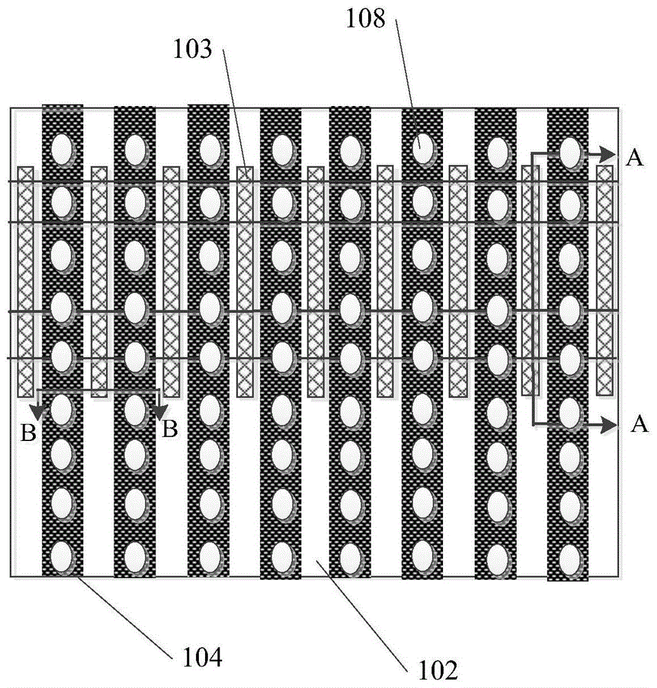
图2是本公开实施例的一种显示面板示意图。参见图2,显示面板包括显示区域AA、弯折区域H和绑定区域B,弯折区域H位于显示区域AA和绑定区域B之间。显示区域通过弯折区域上的数据线与绑定区域进行电连接,实现绑定区域至显示区域的电信号的传输。FIG. 2 is a schematic diagram of a display panel according to an embodiment of the present disclosure. Referring to FIG. 2 , the display panel includes a display area AA, a bending area H and a binding area B, and the bending area H is located between the display area AA and the binding area B. The display area is electrically connected to the binding area through the data lines on the bending area, so as to realize the transmission of electrical signals from the binding area to the display area.
本公开中,显示面板包括显示区域AA、弯折区域H和绑定区域 B的膜层结构不相同,弯折区域H用于弯折,不具有触摸功能和显示功能,显示区域AA用于触摸和显示画面,绑定区域B与驱动电路连接。驱动信号经过绑定区域B和弯折区域H传输至显示区域AA,因此在弯折区域需要设置有数据线。In the present disclosure, the display panel includes a display area AA, a bending area H, and a binding area B with different film layer structures. The bending area H is used for bending and has no touch function and display function, and the display area AA is used for touch And the display screen, the binding area B is connected with the driving circuit. The driving signal is transmitted to the display area AA through the binding area B and the bending area H, so a data line needs to be provided in the bending area.
图3示出了图2的C-C截面图。参见图3,弯折区域包括依次层叠设置的基底101、缓冲层102、间隔排列的SD(Source Drain,简称源漏极)数据线104和平坦层106,绑定区域的信号通过弯折区域的 SD数据线传输到显示区域。其中,基底为柔性基底,材料可以是聚酰亚胺,从而使显示器件可以进行弯曲、弯折或拉伸。请参考图2和图 3,为了便于弯折,弯折区域的缓冲层采用凹槽107设计,该凹槽107 沿着显示区域AA的边缘延伸。图案化SD金属层形成间隔排列的数据线104时,凹槽107的边缘107-1的台阶斜面部分的SD金属层不易刻蚀容易形成SD金属残留211,使得相邻的SD数据线容易短接,造成 X暗线风险,如图1所示。FIG. 3 shows the C-C sectional view of FIG. 2 . Referring to FIG. 3, the bending area includes a
为了解决上述技术问题,本公开提供如下技术方案。In order to solve the above technical problems, the present disclosure provides the following technical solutions.
请参考图2至图7,一种显示面板,包括显示区域AA、弯折区域 H和绑定区域B,弯折区域H位于显示区域AA和绑定区域B之间,该弯折区域H依次设置有基底101、缓冲层102和间隔排列的数据线104,Please refer to FIG. 2 to FIG. 7 , a display panel includes a display area AA, a bending area H and a binding area B, the bending area H is located between the display area AA and the binding area B, and the bending area H is in
缓冲层102的表面为凹槽107,凹槽107沿着显示区域的边缘延伸,该凹槽的边缘107-1包括至少一个斜面111;The surface of the
数据线104设置在缓冲层102上,将绑定区域B的电信号传输至显示区域AA;The
其中,相邻的数据线之间的斜面111上设置有凸起件103,该凸起件 103采用绝缘材料。Wherein, a protruding
凸起件103的材料可以采用树脂,或者采用具有绝缘作用的材料。其中,间隔排列的数据线104是通过图案化形成,也就是整个弯折区域H设置金属层后,通过刻蚀获得所需的图案。此时的金属层可以为SD金属层,或者其他可以导电的金属。如图5所示,该实施方案中,形成的数据线104的图案为纵向间隔排列的图案,与沿着显示区域边缘延伸的凹槽107相互垂直。又如图2所示,与弯折区域相邻的显示区域边缘位于横向上,因此凹槽107在横向上从弯折区域的一端一直延伸到另一端。显然在凹槽的边缘107-1将设置有数据线104。而斜面 111上的相邻数据线104之间因金属残留容易造成短接。在容易形成 SD金属残留的数据线之间的斜面上设置了凸起件103,能够有效防止 SD金属残留的形成。The material of the protruding
在一些实施例中,凸起件的宽度W1小于等于相邻的数据线之间的距离W2。工艺步骤上,形成凸起件103之后图案化金属层形成间隔排列的数据线,因此为了不影响后期数据线的形成,凸起件的宽度W1应小于相邻的数据线之间的距离W2。可以理解的是,在相关设备能够满足足够精准度的前提下,不排除凸起件103的宽度W1等于相邻的数据线104 之间的距离W2的可能。In some embodiments, the width W1 of the protruding member is less than or equal to the distance W2 between adjacent data lines. In the process steps, after forming the
在一些实施例中,凸起件的高度h1大于数据线的高度h2。凸起件的高度h1大于数据线的高度h2时,根据自上而下刻蚀的特点,能够完全刻蚀掉凸起件103上方的金属层,从而解决了相邻的数据线104因金属残留而短接的问题。In some embodiments, the height h1 of the protrusion is greater than the height h2 of the data line. When the height h1 of the protruding member is greater than the height h2 of the data line, according to the characteristics of top-down etching, the metal layer above the protruding
如图5所示,在一些实施例中,数据线104上设置有多个过孔108。该过孔108能够减少应力的集中,起到阻挡裂纹扩散的作用。过孔108 的形状可以是椭圆、圆形、长方形等,这里不做限定,根据应用场景设定。As shown in FIG. 5 , in some embodiments, a plurality of
在一些实施例中,凹槽107的边缘为梯形台阶,包括依次设置的第一台阶和第二台阶,第一台阶靠近凹槽107底部,第二台阶远离凹槽107 底部。其中,第一台阶包括斜面111-1,第二台阶包括斜面111-2。根据应用场景,凹槽107的边缘可以包括一个台阶、两个台阶或者多个台阶。这里以两个台阶为例进行说明。因为金属残留形成在金属层的垂直厚度较大的台阶斜面上,所以该凸起件应覆盖所有的斜面。在一些实施例中,凸起件103为长条形。凸起件103的起点1位于第二台阶的台面,终点2 位于凹槽的底部,并覆盖部分凹槽底部。以边缘包括两个台阶为例,凸起件应覆盖所有的斜面,包括斜面111-1和斜面111-2。因此起点1位于第二台阶的台面,一直延申到凹槽107的底部终点2的位置。至于凸起件107覆盖凹槽底部的多少,可根据应用场景设定,这里不做限定。需要说明的是,根据应用场景,凸起件103还可以采用椭圆形等其他形状。In some embodiments, the edge of the
在一些实施例中,显示面板还包括覆盖整个弯折区域的平坦层106,平坦层106位于数据线104的上方。平坦层106起到平坦化间隔排列的数据线104的凹凸面的作用,为后期的工艺提供平坦的表面。可以理解的是,该平坦层将填充数据线104上的过孔108。In some embodiments, the display panel further includes a
本公开还提供一种显示装置,该显示装置包括本公开的各实施例所提供的显示面板。The present disclosure also provides a display device including the display panel provided by the various embodiments of the present disclosure.
图8示出了显示面板制造方法的示例性流程图。如图8所示,本公开还提供一种显示面板的制造方法,该方法包括如下步骤。显示面板包括显示区域、弯折区域和绑定区域,其中,弯折区域根据如下方式形成:FIG. 8 shows an exemplary flowchart of a method of manufacturing a display panel. As shown in FIG. 8 , the present disclosure further provides a manufacturing method of a display panel, the method includes the following steps. The display panel includes a display area, a bending area and a binding area, wherein the bending area is formed as follows:
步骤S101:提供基板;Step S101: providing a substrate;
步骤S102:在基板上依次形成基底和缓冲层;Step S102: forming a base and a buffer layer on the substrate in sequence;
步骤S103:在缓冲层上形成凹槽,凹槽沿着显示区域的边缘延伸,该凹槽的边缘包括斜面;Step S103: forming a groove on the buffer layer, the groove extends along the edge of the display area, and the edge of the groove includes a slope;
步骤S104:在斜面上形成间隔排列的多个凸起件;Step S104: forming a plurality of protruding pieces arranged at intervals on the inclined surface;
步骤S105:形成金属层,并图案化金属层形成多根间隔排列的数据线,使得凸起件位于相邻的数据线之间;Step S105: forming a metal layer, and patterning the metal layer to form a plurality of data lines arranged at intervals, so that the protrusions are located between adjacent data lines;
步骤S106:形成覆盖整个弯折区域的平坦层。Step S106 : forming a flat layer covering the entire bending area.
下面结合附图2至附图7进行说明。The following description will be made with reference to Fig. 2 to Fig. 7 .
在步骤S101中,该基板可以为玻璃基板。In step S101, the substrate may be a glass substrate.
在步骤S102中,弯折区域H可与显示区域AA同时制造,此时,弯折区域H可以保留所需的显示区域AA的膜层而刻蚀掉不需要的膜层。所需的膜层包括基底101和缓冲层102,该基底101可以是柔性基底,材料可以是聚酰亚胺,从而使显示器件可以进行弯曲、弯折或拉伸。缓冲层102可以是显示区域的一个膜层或者为多个膜层,根据应用场景而确定。In step S102, the bending area H may be fabricated simultaneously with the display area AA. At this time, the bending area H may retain the desired film layer of the display area AA and etch away the unnecessary film layer. The required film layers include a
在步骤S103中,为了使得弯折区域H实现易于弯折,在缓冲层102 上形成凹槽107,凹槽107沿着显示区域AA的边缘延伸。凹槽107的边缘还包括斜面111。例如,凹槽的边缘为梯形台阶形状,或者带有斜面的边缘其他形状。In step S103, in order to make the bending area H easy to bend, a
步骤S104:在斜面111上形成多个凸起件103,该凸起件103采用间隔排列方式;Step S104: forming a plurality of protruding
在步骤S105中,形成数据线105采用图案化工艺,对整层的金属层刻蚀后获得所需的间隔排列的数据线104图案,数据线104垂直于凹槽延伸方向,凸起件103位于数据线之间;In step S105, a patterning process is used to form the data lines 105, and the required pattern of the
在步骤S106中,形成覆盖整个弯折区域的平坦层106。In step S106, a
以上描述仅为本公开的较佳实施例以及对所运用技术原理的说明。本领域技术人员应当理解,本公开中所涉及的发明范围,并不限于上述技术特征的特定组合而成的技术方案,同时也应涵盖在不脱离所述发明构思的情况下,由上述技术特征或其等同特征进行任意组合而形成的其它技术方案。例如上述特征与本公开中公开的(但不限于) 具有类似功能的技术特征进行互相替换而形成的技术方案。The above description is merely a preferred embodiment of the present disclosure and an illustration of the technical principles employed. Those skilled in the art should understand that the scope of the invention involved in the present disclosure is not limited to the technical solutions formed by the specific combination of the above-mentioned technical features, and should also cover the above-mentioned technical features without departing from the inventive concept. Other technical solutions formed by any combination of its equivalent features. For example, a technical solution is formed by replacing the above-mentioned features with the technical features disclosed in the present disclosure (but not limited to) with similar functions.
Claims (10)
Priority Applications (1)
| Application Number | Priority Date | Filing Date | Title |
|---|---|---|---|
| CN202010295790.6A CN111430435B (en) | 2020-04-15 | 2020-04-15 | Display panel, display device, and method for manufacturing display panel |
Applications Claiming Priority (1)
| Application Number | Priority Date | Filing Date | Title |
|---|---|---|---|
| CN202010295790.6A CN111430435B (en) | 2020-04-15 | 2020-04-15 | Display panel, display device, and method for manufacturing display panel |
Publications (2)
| Publication Number | Publication Date |
|---|---|
| CN111430435A true CN111430435A (en) | 2020-07-17 |
| CN111430435B CN111430435B (en) | 2022-12-06 |
Family
ID=71554559
Family Applications (1)
| Application Number | Title | Priority Date | Filing Date |
|---|---|---|---|
| CN202010295790.6A Active CN111430435B (en) | 2020-04-15 | 2020-04-15 | Display panel, display device, and method for manufacturing display panel |
Country Status (1)
| Country | Link |
|---|---|
| CN (1) | CN111430435B (en) |
Citations (5)
| Publication number | Priority date | Publication date | Assignee | Title |
|---|---|---|---|---|
| JP2005328041A (en) * | 2004-04-14 | 2005-11-24 | Mitsubishi Chemicals Corp | Etching method and etching solution |
| CN102479701A (en) * | 2010-11-30 | 2012-05-30 | 中国科学院微电子研究所 | Chemical-mechanical planarization method and fabrication method of back metal gate |
| CN103426820A (en) * | 2013-08-19 | 2013-12-04 | 深圳市华星光电技术有限公司 | Method for avoiding short circuit of metal wires in organic light emitting diode display device |
| WO2019186842A1 (en) * | 2018-03-28 | 2019-10-03 | シャープ株式会社 | Method for producing display device |
| CN110797352A (en) * | 2019-11-08 | 2020-02-14 | 京东方科技集团股份有限公司 | Display panel, manufacturing method thereof and display device |
-
2020
- 2020-04-15 CN CN202010295790.6A patent/CN111430435B/en active Active
Patent Citations (5)
| Publication number | Priority date | Publication date | Assignee | Title |
|---|---|---|---|---|
| JP2005328041A (en) * | 2004-04-14 | 2005-11-24 | Mitsubishi Chemicals Corp | Etching method and etching solution |
| CN102479701A (en) * | 2010-11-30 | 2012-05-30 | 中国科学院微电子研究所 | Chemical-mechanical planarization method and fabrication method of back metal gate |
| CN103426820A (en) * | 2013-08-19 | 2013-12-04 | 深圳市华星光电技术有限公司 | Method for avoiding short circuit of metal wires in organic light emitting diode display device |
| WO2019186842A1 (en) * | 2018-03-28 | 2019-10-03 | シャープ株式会社 | Method for producing display device |
| CN110797352A (en) * | 2019-11-08 | 2020-02-14 | 京东方科技集团股份有限公司 | Display panel, manufacturing method thereof and display device |
Also Published As
| Publication number | Publication date |
|---|---|
| CN111430435B (en) | 2022-12-06 |
Similar Documents
| Publication | Publication Date | Title |
|---|---|---|
| CN108447872B (en) | Array substrate, method for making the same, and display device | |
| CN110085552B (en) | Display panel, display device and manufacturing method of display panel | |
| CN104617106B (en) | A kind of array base palte and display device | |
| WO2021036164A1 (en) | Display panel and manufacturing method therefor | |
| US20170177105A1 (en) | Bezel structure of touch screen and method for manufacturing the same, touch screen and display device | |
| US20200067026A1 (en) | Display panel, method for manufacturing the same and display device | |
| WO2020118990A1 (en) | Display panel | |
| US12336286B2 (en) | Display panel comprising display region and narrow width non-display region and manufacturing method thereof | |
| EP4002477B1 (en) | Display device and method of providing the same | |
| CN107026177A (en) | A kind of COA substrates and preparation method thereof, display device | |
| CN115275044B (en) | display panel | |
| CN110161740A (en) | A kind of display panel and preparation method thereof, display device | |
| CN112735262A (en) | Display substrate, manufacturing method thereof and display device | |
| CN104216159B (en) | A kind of display panel and preparation method thereof, display device | |
| CN104614911A (en) | Substrate as well as manufacturing method and display device thereof | |
| CN111863931B (en) | Display panel and display device | |
| US20160254284A1 (en) | Array substrate, method of preparing the same, and display device | |
| CN111430435B (en) | Display panel, display device, and method for manufacturing display panel | |
| CN110164871A (en) | Tft array substrate and its manufacturing method | |
| CN109659310A (en) | The production method of dot structure and dot structure | |
| TWI595298B (en) | Display panel | |
| CN104849930B (en) | Array base palte and preparation method thereof and display device | |
| CN113113458B (en) | Display panel and display device | |
| US9679924B2 (en) | Array substrate and manufacturing method thereof, display device | |
| CN107368220B (en) | Electronic component |
Legal Events
| Date | Code | Title | Description |
|---|---|---|---|
| PB01 | Publication | ||
| PB01 | Publication | ||
| SE01 | Entry into force of request for substantive examination | ||
| SE01 | Entry into force of request for substantive examination | ||
| GR01 | Patent grant | ||
| GR01 | Patent grant |