CN111415606A - Display device and driving method of display device - Google Patents
Display device and driving method of display device Download PDFInfo
- Publication number
- CN111415606A CN111415606A CN202010005130.XA CN202010005130A CN111415606A CN 111415606 A CN111415606 A CN 111415606A CN 202010005130 A CN202010005130 A CN 202010005130A CN 111415606 A CN111415606 A CN 111415606A
- Authority
- CN
- China
- Prior art keywords
- value
- grayscale
- compensation
- compensated
- gray
- Prior art date
- Legal status (The legal status is an assumption and is not a legal conclusion. Google has not performed a legal analysis and makes no representation as to the accuracy of the status listed.)
- Granted
Links
- 238000000034 method Methods 0.000 title abstract description 45
- 230000004044 response Effects 0.000 claims description 16
- 230000003247 decreasing effect Effects 0.000 claims description 5
- 238000013507 mapping Methods 0.000 claims description 3
- 238000010586 diagram Methods 0.000 description 39
- 230000007423 decrease Effects 0.000 description 11
- 230000008569 process Effects 0.000 description 9
- 230000006870 function Effects 0.000 description 8
- 239000003990 capacitor Substances 0.000 description 7
- 230000006866 deterioration Effects 0.000 description 7
- 230000002829 reductive effect Effects 0.000 description 7
- 238000012360 testing method Methods 0.000 description 7
- 238000006243 chemical reaction Methods 0.000 description 5
- 230000009467 reduction Effects 0.000 description 4
- 230000000670 limiting effect Effects 0.000 description 3
- 230000003071 parasitic effect Effects 0.000 description 3
- 230000036961 partial effect Effects 0.000 description 3
- 230000015556 catabolic process Effects 0.000 description 2
- 230000008859 change Effects 0.000 description 2
- 238000006731 degradation reaction Methods 0.000 description 2
- 230000000694 effects Effects 0.000 description 2
- 238000004519 manufacturing process Methods 0.000 description 2
- 238000012986 modification Methods 0.000 description 2
- 230000004048 modification Effects 0.000 description 2
- 230000008901 benefit Effects 0.000 description 1
- 230000008878 coupling Effects 0.000 description 1
- 238000010168 coupling process Methods 0.000 description 1
- 238000005859 coupling reaction Methods 0.000 description 1
- 230000001419 dependent effect Effects 0.000 description 1
- 238000013461 design Methods 0.000 description 1
- 238000001914 filtration Methods 0.000 description 1
- 239000012530 fluid Substances 0.000 description 1
- 230000003287 optical effect Effects 0.000 description 1
- 230000002441 reversible effect Effects 0.000 description 1
- 239000004065 semiconductor Substances 0.000 description 1
- 230000002123 temporal effect Effects 0.000 description 1
- 238000012546 transfer Methods 0.000 description 1
Images


Classifications
-
- G—PHYSICS
- G09—EDUCATION; CRYPTOGRAPHY; DISPLAY; ADVERTISING; SEALS
- G09G—ARRANGEMENTS OR CIRCUITS FOR CONTROL OF INDICATING DEVICES USING STATIC MEANS TO PRESENT VARIABLE INFORMATION
- G09G3/00—Control arrangements or circuits, of interest only in connection with visual indicators other than cathode-ray tubes
- G09G3/20—Control arrangements or circuits, of interest only in connection with visual indicators other than cathode-ray tubes for presentation of an assembly of a number of characters, e.g. a page, by composing the assembly by combination of individual elements arranged in a matrix no fixed position being assigned to or needed to be assigned to the individual characters or partial characters
- G09G3/2003—Display of colours
-
- G—PHYSICS
- G09—EDUCATION; CRYPTOGRAPHY; DISPLAY; ADVERTISING; SEALS
- G09G—ARRANGEMENTS OR CIRCUITS FOR CONTROL OF INDICATING DEVICES USING STATIC MEANS TO PRESENT VARIABLE INFORMATION
- G09G3/00—Control arrangements or circuits, of interest only in connection with visual indicators other than cathode-ray tubes
- G09G3/20—Control arrangements or circuits, of interest only in connection with visual indicators other than cathode-ray tubes for presentation of an assembly of a number of characters, e.g. a page, by composing the assembly by combination of individual elements arranged in a matrix no fixed position being assigned to or needed to be assigned to the individual characters or partial characters
- G09G3/22—Control arrangements or circuits, of interest only in connection with visual indicators other than cathode-ray tubes for presentation of an assembly of a number of characters, e.g. a page, by composing the assembly by combination of individual elements arranged in a matrix no fixed position being assigned to or needed to be assigned to the individual characters or partial characters using controlled light sources
- G09G3/30—Control arrangements or circuits, of interest only in connection with visual indicators other than cathode-ray tubes for presentation of an assembly of a number of characters, e.g. a page, by composing the assembly by combination of individual elements arranged in a matrix no fixed position being assigned to or needed to be assigned to the individual characters or partial characters using controlled light sources using electroluminescent panels
- G09G3/32—Control arrangements or circuits, of interest only in connection with visual indicators other than cathode-ray tubes for presentation of an assembly of a number of characters, e.g. a page, by composing the assembly by combination of individual elements arranged in a matrix no fixed position being assigned to or needed to be assigned to the individual characters or partial characters using controlled light sources using electroluminescent panels semiconductive, e.g. using light-emitting diodes [LED]
- G09G3/3208—Control arrangements or circuits, of interest only in connection with visual indicators other than cathode-ray tubes for presentation of an assembly of a number of characters, e.g. a page, by composing the assembly by combination of individual elements arranged in a matrix no fixed position being assigned to or needed to be assigned to the individual characters or partial characters using controlled light sources using electroluminescent panels semiconductive, e.g. using light-emitting diodes [LED] organic, e.g. using organic light-emitting diodes [OLED]
- G09G3/3225—Control arrangements or circuits, of interest only in connection with visual indicators other than cathode-ray tubes for presentation of an assembly of a number of characters, e.g. a page, by composing the assembly by combination of individual elements arranged in a matrix no fixed position being assigned to or needed to be assigned to the individual characters or partial characters using controlled light sources using electroluminescent panels semiconductive, e.g. using light-emitting diodes [LED] organic, e.g. using organic light-emitting diodes [OLED] using an active matrix
- G09G3/3233—Control arrangements or circuits, of interest only in connection with visual indicators other than cathode-ray tubes for presentation of an assembly of a number of characters, e.g. a page, by composing the assembly by combination of individual elements arranged in a matrix no fixed position being assigned to or needed to be assigned to the individual characters or partial characters using controlled light sources using electroluminescent panels semiconductive, e.g. using light-emitting diodes [LED] organic, e.g. using organic light-emitting diodes [OLED] using an active matrix with pixel circuitry controlling the current through the light-emitting element
-
- G—PHYSICS
- G09—EDUCATION; CRYPTOGRAPHY; DISPLAY; ADVERTISING; SEALS
- G09G—ARRANGEMENTS OR CIRCUITS FOR CONTROL OF INDICATING DEVICES USING STATIC MEANS TO PRESENT VARIABLE INFORMATION
- G09G3/00—Control arrangements or circuits, of interest only in connection with visual indicators other than cathode-ray tubes
- G09G3/20—Control arrangements or circuits, of interest only in connection with visual indicators other than cathode-ray tubes for presentation of an assembly of a number of characters, e.g. a page, by composing the assembly by combination of individual elements arranged in a matrix no fixed position being assigned to or needed to be assigned to the individual characters or partial characters
- G09G3/2007—Display of intermediate tones
- G09G3/2074—Display of intermediate tones using sub-pixels
-
- G—PHYSICS
- G09—EDUCATION; CRYPTOGRAPHY; DISPLAY; ADVERTISING; SEALS
- G09G—ARRANGEMENTS OR CIRCUITS FOR CONTROL OF INDICATING DEVICES USING STATIC MEANS TO PRESENT VARIABLE INFORMATION
- G09G3/00—Control arrangements or circuits, of interest only in connection with visual indicators other than cathode-ray tubes
- G09G3/20—Control arrangements or circuits, of interest only in connection with visual indicators other than cathode-ray tubes for presentation of an assembly of a number of characters, e.g. a page, by composing the assembly by combination of individual elements arranged in a matrix no fixed position being assigned to or needed to be assigned to the individual characters or partial characters
- G09G3/2007—Display of intermediate tones
-
- G—PHYSICS
- G09—EDUCATION; CRYPTOGRAPHY; DISPLAY; ADVERTISING; SEALS
- G09G—ARRANGEMENTS OR CIRCUITS FOR CONTROL OF INDICATING DEVICES USING STATIC MEANS TO PRESENT VARIABLE INFORMATION
- G09G2320/00—Control of display operating conditions
- G09G2320/02—Improving the quality of display appearance
- G09G2320/0204—Compensation of DC component across the pixels in flat panels
-
- G—PHYSICS
- G09—EDUCATION; CRYPTOGRAPHY; DISPLAY; ADVERTISING; SEALS
- G09G—ARRANGEMENTS OR CIRCUITS FOR CONTROL OF INDICATING DEVICES USING STATIC MEANS TO PRESENT VARIABLE INFORMATION
- G09G2320/00—Control of display operating conditions
- G09G2320/02—Improving the quality of display appearance
- G09G2320/0209—Crosstalk reduction, i.e. to reduce direct or indirect influences of signals directed to a certain pixel of the displayed image on other pixels of said image, inclusive of influences affecting pixels in different frames or fields or sub-images which constitute a same image, e.g. left and right images of a stereoscopic display
-
- G—PHYSICS
- G09—EDUCATION; CRYPTOGRAPHY; DISPLAY; ADVERTISING; SEALS
- G09G—ARRANGEMENTS OR CIRCUITS FOR CONTROL OF INDICATING DEVICES USING STATIC MEANS TO PRESENT VARIABLE INFORMATION
- G09G2320/00—Control of display operating conditions
- G09G2320/02—Improving the quality of display appearance
- G09G2320/0238—Improving the black level
-
- G—PHYSICS
- G09—EDUCATION; CRYPTOGRAPHY; DISPLAY; ADVERTISING; SEALS
- G09G—ARRANGEMENTS OR CIRCUITS FOR CONTROL OF INDICATING DEVICES USING STATIC MEANS TO PRESENT VARIABLE INFORMATION
- G09G2320/00—Control of display operating conditions
- G09G2320/02—Improving the quality of display appearance
- G09G2320/0242—Compensation of deficiencies in the appearance of colours
-
- G—PHYSICS
- G09—EDUCATION; CRYPTOGRAPHY; DISPLAY; ADVERTISING; SEALS
- G09G—ARRANGEMENTS OR CIRCUITS FOR CONTROL OF INDICATING DEVICES USING STATIC MEANS TO PRESENT VARIABLE INFORMATION
- G09G2320/00—Control of display operating conditions
- G09G2320/02—Improving the quality of display appearance
- G09G2320/0271—Adjustment of the gradation levels within the range of the gradation scale, e.g. by redistribution or clipping
- G09G2320/0276—Adjustment of the gradation levels within the range of the gradation scale, e.g. by redistribution or clipping for the purpose of adaptation to the characteristics of a display device, i.e. gamma correction
-
- G—PHYSICS
- G09—EDUCATION; CRYPTOGRAPHY; DISPLAY; ADVERTISING; SEALS
- G09G—ARRANGEMENTS OR CIRCUITS FOR CONTROL OF INDICATING DEVICES USING STATIC MEANS TO PRESENT VARIABLE INFORMATION
- G09G2320/00—Control of display operating conditions
- G09G2320/02—Improving the quality of display appearance
- G09G2320/0285—Improving the quality of display appearance using tables for spatial correction of display data
-
- G—PHYSICS
- G09—EDUCATION; CRYPTOGRAPHY; DISPLAY; ADVERTISING; SEALS
- G09G—ARRANGEMENTS OR CIRCUITS FOR CONTROL OF INDICATING DEVICES USING STATIC MEANS TO PRESENT VARIABLE INFORMATION
- G09G2320/00—Control of display operating conditions
- G09G2320/06—Adjustment of display parameters
- G09G2320/0673—Adjustment of display parameters for control of gamma adjustment, e.g. selecting another gamma curve
-
- G—PHYSICS
- G09—EDUCATION; CRYPTOGRAPHY; DISPLAY; ADVERTISING; SEALS
- G09G—ARRANGEMENTS OR CIRCUITS FOR CONTROL OF INDICATING DEVICES USING STATIC MEANS TO PRESENT VARIABLE INFORMATION
- G09G2340/00—Aspects of display data processing
- G09G2340/10—Mixing of images, i.e. displayed pixel being the result of an operation, e.g. adding, on the corresponding input pixels
Landscapes
- Engineering & Computer Science (AREA)
- Physics & Mathematics (AREA)
- Computer Hardware Design (AREA)
- General Physics & Mathematics (AREA)
- Theoretical Computer Science (AREA)
- Control Of Indicators Other Than Cathode Ray Tubes (AREA)
Abstract
公开了显示装置和显示装置的驱动方法。显示装置包括显示单元、数据转换器和数据驱动器,显示单元包括多个像素,数据转换器接收分别与多个像素对应的灰度值,通过将灰度值中的第一灰度范围的灰度值重新映射到第二灰度范围来生成第一经补偿的灰度值,并且通过基于目标像素的相邻像素的第一经补偿的灰度值对目标像素的第一经补偿的灰度值进行补偿来生成第二经补偿的灰度值,并且数据驱动器基于第二经补偿的灰度值来生成数据信号并且将数据信号提供给显示单元的多个像素,其中,目标像素的相邻像素对应于与目标像素相邻的像素,以及其中,相邻像素中的至少一个发射具有与目标像素的颜色不同颜色的光。
A display device and a driving method of the display device are disclosed. The display device includes a display unit, a data converter and a data driver, the display unit includes a plurality of pixels, and the data converter receives grayscale values corresponding to the plurality of pixels respectively, by converting the grayscale values of the first grayscale range in the grayscale values values are remapped to a second grayscale range to generate a first compensated grayscale value, and the first compensated grayscale value of the target pixel is Compensation is performed to generate a second compensated grayscale value, and the data driver generates a data signal based on the second compensated grayscale value and provides the data signal to a plurality of pixels of the display unit, wherein adjacent pixels of the target pixel corresponds to a pixel adjacent to the target pixel, and wherein at least one of the adjacent pixels emits light having a color different from that of the target pixel.
Description
相关申请的交叉引用CROSS-REFERENCE TO RELATED APPLICATIONS
本申请要求于2019年1月4日提交的韩国专利申请第10-2019-0001259号和于2019年9月10日提交的韩国专利申请第10-2019-0112198号的优先权和权益,这些韩国专利申请出于所有目的通过引用并入本文,如同在本文中全面阐述一样。This application claims priority and the benefit of Korean Patent Application No. 10-2019-0001259 filed on January 4, 2019 and Korean Patent Application No. 10-2019-0112198 filed on September 10, 2019, which Korea The patent application is incorporated herein by reference for all purposes as if fully set forth herein.
技术领域technical field
本发明总体上涉及显示装置和显示装置的驱动方法,并且更具体地,涉及能够补偿显示装置的像素中的泄漏电流的显示装置和显示装置的驱动方法。The present invention generally relates to a display device and a driving method of the display device, and more particularly, to a display device and a driving method of the display device capable of compensating for leakage current in pixels of the display device.
背景技术Background technique
显示装置使用外部施加的控制信号在显示面板上显示图像。The display device displays an image on a display panel using an externally applied control signal.
通常,显示装置可包括红色像素、绿色像素和蓝色像素,其中,具体点处(或具体区域中)的颜色可由红色像素、绿色像素和蓝色像素发射的光分量的时间或空间之和来确定。In general, a display device may include red, green, and blue pixels, where the color at a particular point (or in a particular area) may be derived from the temporal or spatial sum of light components emitted by the red, green, and blue pixels Sure.
在具有相对低的灰度值的低灰度范围中,各个像素的伽马特性和像素的白平衡可能被劣化或失真,并且可能无法以期望的亮度和/或颜色准确地显示图像。In a low grayscale range with relatively low grayscale values, the gamma characteristics of individual pixels and the white balance of the pixels may be degraded or distorted, and images may not be displayed accurately with desired brightness and/or color.
在本背景技术部分中公开的上述信息仅用于理解本发明构思的背景,并因此,其可能包含不构成现有技术的信息。The above information disclosed in this Background section is only for an understanding of the background of the inventive concept and therefore it may contain information that does not form the prior art.
发明内容SUMMARY OF THE INVENTION
申请人发现像素中的泄漏电流可能会降低图像品质和/或颜色,尤其是在低灰度范围内。根据本发明的示例性实现方式构造的显示装置以及采用本发明的示例性实现方式的方法可在低灰度范围内防止或减少显示品质的劣化。Applicants have discovered that leakage currents in pixels can degrade image quality and/or color, especially in the low grayscale range. The display device constructed according to the exemplary implementation of the present invention and the method employing the exemplary implementation of the present invention can prevent or reduce the degradation of display quality in the low gray scale range.
本发明构思的额外的特征将在下面的描述中阐述,并且部分地将通过该描述而显而易见,或者可通过实践本发明构思而习得。Additional features of the inventive concept will be set forth in the description that follows, and in part will be apparent from the description, or may be learned by practice of the inventive concept.
根据本发明的一个或更多个实施方式,显示装置包括显示单元、数据转换器和数据驱动器,显示单元包括多个像素,数据转换器接收分别与多个像素对应的灰度值,通过将灰度值中的第一灰度范围的灰度值重新映射到第二灰度范围来生成第一经补偿的灰度值,并且通过基于目标像素的相邻像素的第一经补偿的灰度值对目标像素的第一经补偿的灰度值进行补偿来生成第二经补偿的灰度值,并且数据驱动器基于第二经补偿的灰度值来生成数据信号并且将数据信号提供给显示单元的多个像素,其中,目标像素的相邻像素对应于与目标像素相邻的像素,以及其中,相邻像素中的至少一个发射具有与目标像素的颜色不同颜色的光。According to one or more embodiments of the present invention, a display device includes a display unit, a data converter, and a data driver, the display unit includes a plurality of pixels, the data converter receives grayscale values corresponding to the plurality of pixels, respectively, by converting the grayscale values The grayscale values of the first grayscale range in the degree value are remapped to the second grayscale range to generate a first compensated grayscale value, and the first compensated grayscale value is generated by The first compensated gray value of the target pixel is compensated to generate a second compensated gray value, and the data driver generates a data signal based on the second compensated gray value and provides the data signal to the display unit. a plurality of pixels, wherein adjacent pixels of the target pixel correspond to pixels adjacent to the target pixel, and wherein at least one of the adjacent pixels emits light having a color different from that of the target pixel.
第一灰度范围为第二灰度范围的子集。The first grayscale range is a subset of the second grayscale range.
第一灰度范围可包括第一低灰度范围,并且第二灰度范围可包括第二低灰度范围,第一低灰度范围为第二低灰度范围的子集,并且数据转换器可将第一低灰度范围中的灰度值重新映射为第二低灰度范围中的第一经补偿的灰度值。The first grayscale range may include a first low grayscale range, and the second grayscale range may include a second low grayscale range, the first low grayscale range being a subset of the second low grayscale range, and the data converter Grayscale values in the first low grayscale range may be remapped to first compensated grayscale values in the second low grayscale range.
数据转换器可基于包括第一低灰度值与第二低灰度值之间的映射信息的查找表来生成第一经补偿的灰度值。The data converter may generate the first compensated grayscale value based on a lookup table including mapping information between the first low grayscale value and the second low grayscale value.
数据转换器可通过响应于相邻像素的第一经补偿的灰度值中的一个增加而减小目标像素的第一经补偿的灰度值来生成目标像素的第二经补偿的灰度值。The data converter may generate a second compensated grayscale value of the target pixel by decreasing the first compensated grayscale value of the target pixel in response to an increase in one of the first compensated grayscale values of the adjacent pixel .
数据转换器可基于相邻像素的第一经补偿的灰度值来计算目标像素的补偿值,并且通过从目标像素的第一经补偿的灰度值减去补偿值来计算目标像素的第二经补偿的灰度值。The data converter may calculate the compensation value of the target pixel based on the first compensated gray value of the adjacent pixel, and calculate the second compensation value of the target pixel by subtracting the compensation value from the first compensated gray value of the target pixel. Compensated grayscale value.
数据转换器可通过基于预设补偿系数来计算相邻像素的第一经补偿的灰度值的加权和,从而计算补偿值。The data converter may calculate the compensation value by calculating a weighted sum of the first compensated grayscale values of adjacent pixels based on a preset compensation coefficient.
与相邻像素中位于与目标像素的行相同的行中的第一相邻像素对应的第一补偿系数可不同于与相邻像素中位于与目标像素的列相同的列中的第二相邻像素对应的第二补偿系数。The first compensation coefficient corresponding to a first adjacent pixel of the adjacent pixels located in the same row as that of the target pixel may be different from a second adjacent pixel of the adjacent pixel located in the same column as that of the target pixel. The second compensation coefficient corresponding to the pixel.
第一补偿系数可大于第二补偿系数。The first compensation coefficient may be greater than the second compensation coefficient.
补偿值可与第一经补偿的灰度值成反比。The compensation value may be inversely proportional to the first compensated grayscale value.
补偿值可与多个像素的总的最大亮度成反比。The compensation value may be inversely proportional to the total maximum brightness of the plurality of pixels.
多个像素可包括发射第一颜色的光的第一像素、发射第二颜色的光的第二像素和发射第三颜色的光的第三像素,数据转换器可使用包括第一补偿系数的第一补偿滤波器来计算第一像素的第一补偿值,并且使用包括第二补偿系数的第二补偿滤波器来计算第二像素的第二补偿值,并且第二补偿滤波器可不同于第一补偿滤波器。The plurality of pixels may include a first pixel emitting light of a first color, a second pixel emitting light of a second color, and a third pixel emitting light of a third color, and the data converter may use a first pixel including a first compensation coefficient. a compensation filter to calculate a first compensation value for the first pixel, and a second compensation filter including a second compensation coefficient to calculate a second compensation value for the second pixel, and the second compensation filter may be different from the first compensation Compensation filter.
相邻像素可包括在与目标像素的行相同的行中。Neighboring pixels may be included in the same row as the target pixel's row.
根据本发明的一个或更多个实施方式,显示装置的驱动方法可包括:通过将相应的输入灰度值从第一灰度范围重新映射到第二灰度范围来生成第一经补偿的灰度值;通过基于目标像素的相邻像素的第一经补偿的灰度值对目标像素的第一经补偿的灰度值进行补偿来生成第二经补偿的灰度值;以及基于第二经补偿的灰度值来生成数据信号,其中,目标像素的相邻像素对应于与目标像素相邻地排列的像素,以及其中,相邻像素中的至少一个发射具有与目标像素的颜色不同颜色的光。According to one or more embodiments of the present invention, a driving method of a display device may include generating a first compensated grayscale by remapping corresponding input grayscale values from a first grayscale range to a second grayscale range generating a second compensated gray value by compensating the first compensated gray value of the target pixel based on the first compensated gray value of neighboring pixels of the target pixel; and based on the second compensated gray value compensated grayscale values to generate a data signal, wherein adjacent pixels of the target pixel correspond to pixels arranged adjacent to the target pixel, and wherein at least one of the adjacent pixels emits a color having a color different from that of the target pixel. Light.
生成第二经补偿的灰度值的步骤可包括:通过响应于相邻像素的第一经补偿的灰度值中的一个增加,减小目标像素的第一经补偿的灰度值来生成第二经补偿的灰度值。The generating of the second compensated grayscale value may include generating the first compensated grayscale value by decreasing the first compensated grayscale value of the target pixel in response to an increase in one of the first compensated grayscale values of the adjacent pixel. Two compensated grayscale values.
生成第二经补偿的灰度值的步骤可包括:基于目标像素的第一经补偿的灰度值来确定目标像素的全局增益;以及基于全局增益和相邻像素的第一经补偿的灰度值来计算目标像素的第二经补偿的灰度值。The generating of the second compensated grayscale value may include: determining a global gain of the target pixel based on the first compensated grayscale value of the target pixel; and based on the global gain and the first compensated grayscale of adjacent pixels value to calculate the second compensated gray value of the target pixel.
根据本发明的一个或更多个实施方式,显示装置可包括显示单元、数据转换器和数据驱动器,显示单元包括多个像素,数据转换器接收分别与多个像素对应的灰度值,将灰度值中的第一灰度范围的灰度值重新映射到第二灰度范围来生成第一经补偿的灰度值,并且通过基于目标像素的相邻像素的第一经补偿的灰度值对目标像素的灰度值进行补偿来生成第二经补偿的灰度值,并且数据驱动器基于第二经补偿的灰度值来生成数据信号并且将数据信号提供给多个像素,其中,目标像素的相邻像素对应于与目标像素相邻的像素,以及其中,相邻像素中的至少一个配置成发射与目标像素的颜色不同颜色的光。According to one or more embodiments of the present invention, a display device may include a display unit, a data converter, and a data driver, the display unit includes a plurality of pixels, the data converter receives grayscale values corresponding to the plurality of pixels, respectively, and converts the grayscale values into grayscale values. The grayscale values of the first grayscale range in the degree value are remapped to the second grayscale range to generate a first compensated grayscale value, and the first compensated grayscale value is generated by The gray value of the target pixel is compensated to generate a second compensated gray value, and the data driver generates a data signal based on the second compensated gray value and provides the data signal to the plurality of pixels, wherein the target pixel The adjacent pixels correspond to pixels adjacent to the target pixel, and wherein at least one of the adjacent pixels is configured to emit light of a different color than that of the target pixel.
第二灰度范围可为第一灰度范围的子集。The second grayscale range may be a subset of the first grayscale range.
数据转换器可配置成通过从目标像素的第一经补偿的灰度值减去目标像素的灰度值来计算差值,基于相邻像素的第一经补偿的灰度值来计算目标像素的第一补偿值,通过从差值的绝对值减去第一补偿值来计算第二补偿值,并且基于灰度值和第二补偿值来计算目标像素的第二经补偿的灰度值,并且数据转换器可配置成随着相邻像素的第一经补偿的灰度值中的一个增加而增加第一补偿值。The data converter may be configured to calculate the difference value by subtracting the grayscale value of the target pixel from the first compensated grayscale value of the target pixel, and calculate the difference value of the target pixel based on the first compensated grayscale value of the adjacent pixel. a first compensation value, a second compensation value is calculated by subtracting the first compensation value from the absolute value of the difference, and a second compensated grayscale value of the target pixel is calculated based on the grayscale value and the second compensation value, and The data converter may be configured to increase the first compensation value as one of the first compensated grayscale values of adjacent pixels increases.
数据转换器可配置成响应于第一补偿值小于0而将第一补偿值设置为第二经补偿的灰度值。The data converter may be configured to set the first compensation value to the second compensated grayscale value in response to the first compensation value being less than zero.
数据转换器可配置成通过基于根据相邻像素的第一经补偿的灰度值中相应的第一经补偿的灰度值来预设的补偿系数来计算相邻像素的第一经补偿的灰度值的加权和,从而计算第一补偿值。The data converter may be configured to calculate the first compensated grayscale of the adjacent pixel by presetting a compensation coefficient based on a corresponding first compensated grayscale value of the adjacent pixel A weighted sum of the degree values is used to calculate the first compensation value.
在相邻像素之中,对于相邻像素中位于与目标像素的行相同的行中的第一相邻像素的第一补偿系数可不同于对于相邻像素中位于与目标像素的列相同的列中的第二相邻像素的第二补偿系数。Among adjacent pixels, the first compensation coefficient for a first adjacent pixel located in the same row as that of the target pixel among the adjacent pixels may be different from that for the adjacent pixel located in the same column as that of the target pixel The second compensation coefficient of the second neighboring pixel in .
数据转换器可配置成通过响应于差值大于0而将第一经补偿的灰度值加到第二补偿值来计算第二经补偿的灰度值。The data converter may be configured to calculate the second compensated grayscale value by adding the first compensated grayscale value to the second compensated value in response to the difference being greater than zero.
数据转换器可配置成通过响应于差值小于0而从第一经补偿的灰度值减去第二补偿值来计算第二经补偿的灰度值。The data converter may be configured to calculate the second compensated grayscale value by subtracting the second compensated value from the first compensated grayscale value in response to the difference being less than zero.
第一补偿值可与目标像素的灰度值成正比,并且可与第一经补偿的灰度值成反比。The first compensation value may be proportional to the gray value of the target pixel, and may be inversely proportional to the first compensated gray value.
根据本发明实施方式的显示装置和显示装置的驱动方法可通过重新映射低灰度范围内的灰度值来补偿相应的像素的伽马特性的劣化,并且可通过基于相邻灰度值补偿重新映射的灰度值来校正像素的白平衡中的失真(不当)。因此,可减轻或防止在低灰度范围内的显示品质的劣化。The display device and the driving method of the display device according to the embodiments of the present invention can compensate for the deterioration of the gamma characteristic of the corresponding pixel by remapping the grayscale values in the low grayscale range, and can compensate for the degradation of the gamma characteristic of the corresponding pixel by Mapped grayscale values to correct for distortion (improper) in the pixel's white balance. Therefore, the deterioration of the display quality in the low gradation range can be reduced or prevented.
应理解,前面的一般描述和下面的详细描述都是示例性和解释性的,并且旨在提供对所要求保护的本发明的进一步解释。It is to be understood that both the foregoing general description and the following detailed description are exemplary and explanatory and are intended to provide further explanation of the invention as claimed.
附图说明Description of drawings
附图被包括以提供对本发明的进一步理解,并且被并入并构成本说明书的一部分,附图示出了本发明的示例性实施方式,并且与描述一同用于解释本发明构思。The accompanying drawings, which are included to provide a further understanding of the invention and are incorporated in and constitute a part of this specification, illustrate exemplary embodiments of the invention and together with the description serve to explain the inventive concept.
图1是根据本发明的示例性实施方式构造的显示装置的框图。FIG. 1 is a block diagram of a display device constructed in accordance with an exemplary embodiment of the present invention.
图2是示出图1的显示装置中的示例性像素的等效电路的电路图。FIG. 2 is a circuit diagram illustrating an equivalent circuit of an exemplary pixel in the display device of FIG. 1 .
图3是示出图2的像素与相邻像素之间的关系的局部电路图。FIG. 3 is a partial circuit diagram showing the relationship between the pixel of FIG. 2 and adjacent pixels.
图4是示出可归因于图3的相邻像素的对应像素的发光特性中的变化的曲线图。FIG. 4 is a graph showing changes in light emission characteristics attributable to the corresponding pixels of the adjacent pixels of FIG. 3 .
图5是示出图1的显示装置中的控制器的示例的框图。FIG. 5 is a block diagram illustrating an example of a controller in the display device of FIG. 1 .
图6是用于解释由图5的控制器中的第一数据补偿器执行的灰度重新映射的曲线图。FIG. 6 is a graph for explaining grayscale remapping performed by the first data compensator in the controller of FIG. 5 .
图7是示出可在图5的控制器中的第一数据补偿器中使用的查找表的示例的图。FIG. 7 is a diagram illustrating an example of a look-up table that may be used in the first data compensator in the controller of FIG. 5 .
图8是示出图5的控制器的伽马曲线中的变化的构思图。FIG. 8 is a conceptual diagram illustrating changes in the gamma curve of the controller of FIG. 5 .
图9A是示出在图5的控制器中的第二数据补偿器中使用的补偿滤波器的示例的图。FIG. 9A is a diagram showing an example of a compensation filter used in the second data compensator in the controller of FIG. 5 .
图9B是示出图9A的补偿滤波器的实施方式的图。FIG. 9B is a diagram illustrating an embodiment of the compensation filter of FIG. 9A .
图10是示出图5的控制器使用图9A的补偿滤波器来补偿灰度值的处理的示例的图。FIG. 10 is a diagram illustrating an example of a process in which the controller of FIG. 5 uses the compensation filter of FIG. 9A to compensate gradation values.
图11是示出图5的控制器使用图9A的补偿滤波器来补偿灰度值的处理的示例的图。FIG. 11 is a diagram illustrating an example of a process in which the controller of FIG. 5 uses the compensation filter of FIG. 9A to compensate gradation values.
图12是示出在图5的控制器中使用的第一增益的示例的曲线图。FIG. 12 is a graph showing an example of a first gain used in the controller of FIG. 5 .
图13是示出在图5的控制器中使用的第二增益的示例的曲线图。FIG. 13 is a graph showing an example of a second gain used in the controller of FIG. 5 .
图14是示出包括在图5的控制器中的第二数据补偿器的示例的框图。FIG. 14 is a block diagram illustrating an example of a second data compensator included in the controller of FIG. 5 .
图15是示出包括在图5的控制器中的第二数据补偿器的示例的框图。FIG. 15 is a block diagram illustrating an example of a second data compensator included in the controller of FIG. 5 .
图16A是示出由图15的第二数据补偿器为白色图像计算的补偿值的图。FIG. 16A is a diagram showing compensation values calculated by the second data compensator of FIG. 15 for a white image.
图16B是示出由图15的第二数据补偿器为单色图像计算的补偿值的图。FIG. 16B is a diagram showing compensation values calculated by the second data compensator of FIG. 15 for a monochrome image.
图17是示出提供给图5的控制器的测试数据的示例的图。FIG. 17 is a diagram showing an example of test data provided to the controller of FIG. 5 .
图18是示出图5的控制器使用图9A的补偿滤波器来补偿灰度值的处理的示例的图。FIG. 18 is a diagram illustrating an example of a process in which the controller of FIG. 5 uses the compensation filter of FIG. 9A to compensate gradation values.
图19是示出包括在图5的控制器中的第二数据补偿器中使用的补偿滤波器的各种示例的图。FIG. 19 is a diagram showing various examples of compensation filters used in the second data compensator included in the controller of FIG. 5 .
图20是示出在图5的控制器中的第二数据补偿器中使用的补偿滤波器的示例的图。FIG. 20 is a diagram showing an example of a compensation filter used in the second data compensator in the controller of FIG. 5 .
图21是示出根据本发明的示例性实施方式的显示装置的驱动方法的流程图。FIG. 21 is a flowchart illustrating a driving method of a display device according to an exemplary embodiment of the present invention.
图22是示出根据本发明的示例性实施方式的显示装置的驱动方法的流程图。FIG. 22 is a flowchart illustrating a driving method of a display device according to an exemplary embodiment of the present invention.
具体实施方式Detailed ways
在下面的描述中,为了解释的目的,阐述了许多具体细节以提供对本发明的各种示例性实施方式或实现方式的透彻理解。如本文中所使用的,“实施方式”和“实现方式”为可互换的词,它们是采用本文中所公开的本发明构思中的一种或更多种的装置或方法的非限制性示例。然而,显而易见的是,各种示例性实施方式可在没有这些具体细节的情况下或者用一个或更多个等同布置的情况下实践。在其它实例中,公知的结构和装置以框图形式示出以避免不必要地混淆各种示例性实施方式。此外,各种示例性实施方式可为不同的,但不必是排他的。例如,在不背离本发明构思的情况下,示例性实施方式的具体形状、配置和特性可使用或实现在另一示例性实施方式中。In the following description, for the purposes of explanation, numerous specific details are set forth in order to provide a thorough understanding of various exemplary embodiments or implementations of the present invention. As used herein, "embodiment" and "implementation" are interchangeable words that are non-limiting means of employing one or more of the inventive concepts disclosed herein or methods Example. It will be apparent, however, that various exemplary embodiments may be practiced without these specific details or with one or more equivalent arrangements. In other instances, well-known structures and devices are shown in block diagram form in order to avoid unnecessarily obscuring the various example embodiments. Furthermore, the various exemplary embodiments may be different, but not necessarily exclusive. For example, the specific shapes, configurations and characteristics of an exemplary embodiment may be used or implemented in another exemplary embodiment without departing from the inventive concept.
除非另有指示,否则所示的示例性实施方式应被理解为提供能够在实践中实现本发明构思的一些方式的不同细节的示例性特征。因此,除非另有指示,否则各种实施方式的特征、部件、模块、层、膜、面板、区和/或方面等(在下文中单独称为或统称为“元件”)可在不背离本发明构思的情况下以其它方式组合、分离、互换和/或重新布置。Unless otherwise indicated, the exemplary embodiments shown are to be understood as providing exemplary features of various details that can enable some ways of implementing the inventive concepts in practice. Thus, unless otherwise indicated, the features, components, modules, layers, films, panels, regions and/or aspects, etc. of the various embodiments (hereinafter individually or collectively referred to as "elements") may be implemented without departing from the invention Otherwise combined, separated, interchanged and/or rearranged where contemplated.
在附图中,出于清楚和/或描述的目的,元件的尺寸和相对尺寸可被夸大。当示例性实施方式可不同地实现时,具体工艺顺序可与所描述的顺序不同地执行。例如,两个连续描述的工艺可基本上同时执行或者以与描述的顺序相反的顺序执行。而且,相同的附图标记表示相同的元件。In the drawings, the size and relative sizes of elements may be exaggerated for clarity and/or description. When the exemplary embodiments may be implemented differently, the specific process sequence may be performed differently from the described sequence. For example, two processes described in succession may be performed substantially concurrently or in the reverse order from that described. Also, the same reference numerals denote the same elements.
当元件或层被称为“在”另一元件或层“上”、“连接到”或“耦接到”另一元件或层时,该元件或层可直接在另一元件或层上、连接到或耦接到另一元件或层,或者可存在有中间元件或层。然而,当元件或层被称为“直接在”另一元件或层“上”、“直接连接到”或“直接耦接到”另一元件或层时,则不存在中间元件或层。为此,术语“连接”可指示在具有或不具有中间元件的情况下的物理的、电气的和/或流体的连接。为了这种公开的目的,“X、Y和Z中的至少一个”和“选自由X、Y和Z构成的集群中的至少一个”可被解释为仅X、仅Y、仅Z,或者X、Y和Z中的两个或更多个的任何组合,诸如例如XYZ、XYY、YZ和ZZ。如本文中所使用的,术语“和/或”包括相关所列项目中的一个或更多个的任何和所有组合。When an element or layer is referred to as being "on," "connected to," or "coupled to" another element or layer, the element or layer can be directly on, connected or coupled to another element or layer, or intervening elements or layers may be present. However, when an element or layer is referred to as being "directly on," "directly connected to," or "directly coupled to" another element or layer, there are no intervening elements or layers present. To this end, the term "connected" may indicate a physical, electrical and/or fluid connection with or without intervening elements. For the purposes of this disclosure, "at least one of X, Y, and Z" and "at least one selected from the group consisting of X, Y, and Z" may be interpreted as X only, Y only, Z only, or X only Any combination of two or more of , Y, and Z, such as, for example, XYZ, XYY, YZ, and ZZ. As used herein, the term "and/or" includes any and all combinations of one or more of the associated listed items.
尽管术语“第一”、“第二”等可在本文中用于描述各种类型的元件,但是这些元件不应受这些术语的限制。这些术语用于将一个元件与另一元件区分开。因此,在不背离本公开的教导的情况下,下面讨论的第一元件可被称为第二元件。Although the terms "first," "second," etc. may be used herein to describe various types of elements, these elements should not be limited by these terms. These terms are used to distinguish one element from another element. Thus, a first element discussed below could be termed a second element without departing from the teachings of the present disclosure.
空间相对术语诸如“下面(beneath)”、“下方(below)”、“在...之下(under)”、“下(lower)”、“上方(above)”、“上(upper)”、“越过(over)”、“更高(higher)”、“侧(side)”(例如,如在“侧壁(sidewall)”中)等可在本文中出于描述性目的使用,并因此,用以描述如附图中所示的一个元件与另一元件的关系。除了附图中描绘的取向以外,空间相对术语还旨在包含器件在使用、操作和/或制造中的不同取向。例如,如果附图中的器件被翻转,则被描述为在其它元件或特征“下方”或“下面”的元件将随后被取向为在其它元件或特征“上方”。因此,示例性术语“下方”可包含上方和下方的取向这两者。此外,器件可为其它方式取向(例如,旋转90度或在其它取向),并由此,本文中使用的空间相对描述词被相应地解释。Spatially relative terms such as "beneath", "below", "under", "lower", "above", "upper" , "over", "higher", "side" (eg, as in "sidewall"), etc. may be used herein for descriptive purposes, and thus , to describe the relationship of one element to another element as shown in the figures. In addition to the orientation depicted in the figures, spatially relative terms are intended to encompass different orientations of the device in use, operation, and/or manufacture. For example, if the device in the figures is turned over, elements described as "below" or "beneath" other elements or features would then be oriented "above" the other elements or features. Thus, the exemplary term "below" can encompass both an orientation of above and below. In addition, the device may be otherwise oriented (eg, rotated 90 degrees or at other orientations) and thus, the spatially relative descriptors used herein are interpreted accordingly.
本文中所使用的术语是出于描述特定实施方式的目的,而不旨在限制。除非上下文另有明确说明,否则如本文所使用的单数形式“一(a)”、“一(an)”和“该(the)”也旨在包括复数形式。此外,当术语“包括(comprise)”、“包括有(comprising)”、“包含(include)”和/或“包含有(including)”在本说明书中使用时,指示所陈述的特征、整体、步骤、操作、元件、部件和/或其集群的存在,但不排除一个或更多个其它特征、整体、步骤、操作、元件、部件和/或其集群的存在或添加。还注意,如本文所使用的,术语“基本上(substantially)”、“约(about)”以及其它相似术语用作近似的术语而不是程度的术语,并且由此,利用于考虑本领域普通技术人员将认识到的测量值、计算值和/或提供值的固有偏差。The terminology used herein is for the purpose of describing particular embodiments and is not intended to be limiting. As used herein, the singular forms "a (a)," "an (an)," and "the (the)" are intended to include the plural forms as well, unless the context clearly dictates otherwise. Furthermore, when the terms "comprise", "comprising", "include" and/or "including" are used in this specification, they are indicative of the stated features, integers, The presence of steps, operations, elements, components and/or clusters thereof does not preclude the presence or addition of one or more other features, integers, steps, operations, elements, components and/or clusters thereof. Note also that, as used herein, the terms "substantially," "about," and other similar terms are used as terms of approximation rather than of degree, and thus, are utilized in consideration of ordinary skill in the art Inherent deviations from measured, calculated and/or provided values that will be recognized by a person.
如本领域中的惯例,在功能块、单元和/或模块方面,在附图中示出并描述了一些示例性实施方式。本领域技术人员将理解,这些块、单元和/或模块通过电子(或光学)电路(诸如可使用基于半导体的制造技术或其它制造技术形成的逻辑电路、分立部件、微处理器、硬连线电路、存储器元件、布线连接等)物理地实现。在由微处理器或其它相似硬件实现的块、单元和/或模块的情况下,可使用软件(例如,微代码)对它们进行编程和控制,以执行本文中所讨论的各种功能,并且可选择性由固件和/或软件来驱动。还预期到每个块、单元和/或模块可由专用硬件实现,或者作为执行一些功能的专用硬件与处理器(例如,一个或更多个编程的微处理器和相关联的电路)的组合来执行其它功能。而且,在不背离本发明构思的范围的情况下,一些示例性实施方式的每个块、单元和/或模块可在物理上分离成两个或更多个交互和分立的块、单元和/或模块。此外,在不背离本发明构思的范围的情况下,一些示例性实施方式的块、单元和/或模块可物理地组合成更复杂的块、单元和/或模块。As is customary in the art, some exemplary embodiments are shown and described in the drawings in terms of functional blocks, units and/or modules. Those skilled in the art will understand that these blocks, units and/or modules are formed by electronic (or optical) circuits such as logic circuits, discrete components, microprocessors, hard-wiring, which may be formed using semiconductor-based or other manufacturing techniques circuits, memory elements, wiring connections, etc.) are physically implemented. In the case of blocks, units and/or modules implemented by a microprocessor or other similar hardware, they may be programmed and controlled using software (eg, microcode) to perform the various functions discussed herein, and Optionally driven by firmware and/or software. It is also contemplated that each block, unit and/or module may be implemented by special purpose hardware, or as a combination of special purpose hardware and a processor (eg, one or more programmed microprocessors and associated circuitry) to perform some functions perform other functions. Furthermore, each block, unit and/or module of some exemplary embodiments may be physically separated into two or more interacting and discrete blocks, units and/or modules without departing from the scope of the present inventive concepts or modules. Furthermore, the blocks, units and/or modules of some example embodiments may be physically combined into more complex blocks, units and/or modules without departing from the scope of the present inventive concept.
除非另有限定,否则本文中所使用的所有术语(包括技术和科学术语)具有与本公开所属技术领域的普通技术人员通常理解的含义相同的含义。除非在本文中明确地这样限定,否则诸如常用词典中限定的那些术语应被解释为具有与它们在相关技术的上下文中的含义一致的含义,并且不应以理想化或过于正式的含义来解释。Unless otherwise defined, all terms (including technical and scientific terms) used herein have the same meaning as commonly understood by one of ordinary skill in the art to which this disclosure belongs. Unless explicitly so defined herein, terms such as those defined in commonly used dictionaries should be construed as having meanings consistent with their meanings in the context of the related art and should not be construed in idealized or overly formal meanings .
在下文中,将参考附图对本发明的实施方式进行详细描述,以使得本领域技术人员可容易地实践本发明。本发明可以以各种不同的形式实施,而不限于以下实施方式。Hereinafter, embodiments of the present invention will be described in detail with reference to the accompanying drawings so that those skilled in the art can easily practice the present invention. The present invention can be implemented in various forms without being limited to the following embodiments.
此外,在附图中,将省略与本发明无关的部分以更清楚地解释本发明。应参考在所有不同的附图中使用相同的附图标记来表示相同的部件的附图。因此,上述附图标记也可在其它附图中使用。In addition, in the drawings, parts unrelated to the present invention will be omitted to explain the present invention more clearly. Reference should be made to drawings in which the same reference numerals are used throughout the different drawings to refer to the same parts. Accordingly, the above reference numbers may also be used in other figures.
图1是根据本发明的示例性实施方式构造的显示装置的框图。FIG. 1 is a block diagram of a display device constructed in accordance with an exemplary embodiment of the present invention.
参照图1,显示装置1可包括显示单元110、数据驱动器120、栅极驱动器130和控制器140。Referring to FIG. 1 , the
显示单元110可显示图像。显示单元110可实现为显示面板。The
显示单元110可包括数据线DL1至DLm(其中,m是正整数)、栅极线GL1至GLn(其中,n是正整数)和像素PX。像素PX可排列在由数据线DL1至DLm和栅极线GL1至GLn划分的区域中。像素PX可电耦接到数据线DL1至DLm和栅极线GL1至GLn。The
例如,布置在第一行和第一列中的像素PX可耦接到第一数据线DL1和第一栅极线GL1。例如,布置在第n行和第m列中的像素PX可耦接到第m数据线DLm和第n栅极线GLn。For example, the pixels PX arranged in the first row and the first column may be coupled to the first data line DL1 and the first gate line GL1. For example, the pixels PX arranged in the n-th row and the m-th column may be coupled to the m-th data line DLm and the n-th gate line GLn.
然而,像素PX的耦接不限于此。例如,每个像素PX可电耦接到与相邻行对应的栅极线(例如,与包括对应像素PX的行之前的行对应的栅极线和与下一行对应的栅极线)。此外,尽管在附图中未示出,但是像素PX可电耦接到第一电源线和第二电源线,并且然后可接收第一电源电压VDD和第二电源电压VSS。此处,第一电源电压VDD和第二电源电压VSS可为驱动像素PX所需的电压。However, the coupling of the pixels PX is not limited to this. For example, each pixel PX may be electrically coupled to a gate line corresponding to an adjacent row (eg, a gate line corresponding to a row preceding the row including the corresponding pixel PX and a gate line corresponding to the next row). Also, although not shown in the drawings, the pixel PX may be electrically coupled to the first and second power supply lines, and may then receive the first and second power supply voltages VDD and VSS. Here, the first power supply voltage VDD and the second power supply voltage VSS may be voltages required for driving the pixels PX.
每个像素PX可响应于通过对应栅极线提供的栅极信号而发射具有与通过对应数据线提供的数据信号对应的亮度的光。稍后将参考图2对每个像素PX的配置和操作进行详细描述。Each pixel PX may emit light having luminance corresponding to the data signal supplied through the corresponding data line in response to the gate signal supplied through the corresponding gate line. The configuration and operation of each pixel PX will be described in detail later with reference to FIG. 2 .
数据驱动器120可基于数据控制信号DCS和图像数据DATA来生成数据信号,并且可将数据信号提供给数据线DL1至DLm。此处,数据控制信号DCS可为用于控制数据驱动器120的操作的信号,并且可包括数据使能信号等。The
数据驱动器120可实现为集成电路(IC)(例如,驱动IC),并且可安装在柔性印刷电路板(FPCB)上,且然后耦接到显示单元110。The
栅极驱动器130(或扫描驱动器)可响应于栅极控制信号GCS而生成栅极信号,并且可将栅极信号提供给栅极线GL1至GLn。此处,栅极控制信号GCS可为用于控制栅极驱动器130的操作的信号,并且可包括起始信号、时钟信号等。例如,栅极驱动器130可使用时钟信号顺序地生成和输出与起始信号对应的栅极信号(例如,具有与起始信号的波形相同或相似的波形的栅极信号)。栅极驱动器130可包括移位寄存器。栅极驱动器130可形成在显示单元110的区(或者显示面板的区)中,或者可实现为IC,并且可安装在柔性印刷电路板(FPCB)上,且然后耦接到显示单元110。The gate driver 130 (or the scan driver) may generate gate signals in response to the gate control signal GCS, and may supply the gate signals to the gate lines GL1 to GLn. Here, the gate control signal GCS may be a signal for controlling the operation of the
控制器140可从外部装置(例如,图形处理器)接收输入图像数据RGB(例如,RGB数据)和控制信号CS,并且可响应于控制信号CS而生成栅极控制信号GCS和数据控制信号DCS。此处,输入图像数据RGB可包括与像素PX对应的灰度值。The
控制信号CS可包括时钟信号、水平同步信号、数据使能信号等。The control signal CS may include a clock signal, a horizontal synchronization signal, a data enable signal, and the like.
此外,控制器140可将输入图像数据RGB转换成与显示单元110的像素阵列匹配的图像数据DATA,并且将图像数据DATA输出到数据驱动器120。Also, the
在示例性实施方式中,控制器140可将包括在输入图像数据RGB中的每个灰度值从第一灰度范围重新映射到第二灰度范围,且然后生成重新映射的灰度值(或第一经补偿的灰度值)。此处,第二灰度范围可窄于第一灰度范围。特别地,第一灰度范围可包含第二灰度范围。例如,控制器140可将从0的灰度值到255的灰度值的第一灰度范围重新映射到从14的灰度值到255的灰度值的第二灰度范围。In an exemplary embodiment, the
此外,控制器140可基于相邻灰度值来补偿目标像素的重新映射的灰度值,且然后可生成目标像素的经补偿的灰度值(或第二经补偿的灰度值)。此处,相邻灰度值可为与排列成与目标像素(即,与待补偿的灰度值对应的像素PX)相邻的相邻像素对应的灰度值(即,重新映射的灰度值),并且相邻像素中的至少一个可发射与目标像素的颜色不同的颜色的光。例如,与包括在第二行和第二列中的像素PX相邻的像素PX可为排列在第一行至第三行与第一列至第三列相交的区域中(或在图1中所示的第一区域A1中)的像素PX中的至少一个。Also, the
在实施方式中,控制器140可基于重新映射的灰度值和相邻灰度值(或相邻像素的重新映射的灰度值)来补偿灰度值,并且可生成经补偿的灰度值(或第二经补偿的灰度值)。In an embodiment, the
在示例性实施方式中,控制器140可通过使目标像素的重新映射的灰度值随着相邻灰度值中的至少一个增加而减小来生成目标像素的经补偿的灰度值。In an exemplary embodiment, the
下面,将与像素PX的结构相关地对允许控制器140对灰度值进行重新映射的灰度重新映射和灰度补偿进行描述。Next, grayscale remapping and grayscale compensation that allow the
尽管在图1中将控制器140示出为与数据驱动器120独立地实现,但是控制器140不限于此。例如,控制器140可与数据驱动器120集成到单个IC中,或者可包括在数据驱动器120中。Although the
图2是示出图1的显示装置中的示例性像素的等效电路的电路图。图3是示出图2的像素与相邻像素之间的关系的局部电路图。FIG. 2 is a circuit diagram illustrating an equivalent circuit of an exemplary pixel in the display device of FIG. 1 . FIG. 3 is a partial circuit diagram showing the relationship between the pixel of FIG. 2 and adjacent pixels.
参照图1和图2,像素PX可包括第一晶体管T1、第二晶体管T2、存储电容器Cst和发光元件LD。1 and 2, the pixel PX may include a first transistor T1, a second transistor T2, a storage capacitor Cst, and a light emitting element LD.
第一晶体管T1和第二晶体管T2可实现为P型晶体管(例如,PMOS晶体管),但是不限于此。例如,第一晶体管T1和第二晶体管T2中的至少一个可实现为N型晶体管(例如,NMOS晶体管)。而且,除了第一晶体管T1和第二晶体管T2之外,像素PX还可包括其它晶体管。The first transistor T1 and the second transistor T2 may be implemented as P-type transistors (eg, PMOS transistors), but are not limited thereto. For example, at least one of the first transistor T1 and the second transistor T2 may be implemented as an N-type transistor (eg, an NMOS transistor). Also, the pixel PX may include other transistors in addition to the first transistor T1 and the second transistor T2.
第一晶体管T1(或驱动晶体管)可包括耦接到施加有第一电源电压VDD的第一电源线的第一电极、耦接到第二节点N2的第二电极和耦接到第一节点N1的栅电极。The first transistor T1 (or driving transistor) may include a first electrode coupled to a first power supply line to which the first power supply voltage VDD is applied, a second electrode coupled to the second node N2, and a second electrode coupled to the first node N1 gate electrode.
第二晶体管T2(或开关晶体管)可包括耦接到数据线DL的第一电极、耦接到第一节点N1的第二电极和耦接到栅极线GL的栅电极。此处,数据线DL可为图1中所示的数据线DL1至DLm中的一个,并且栅极线GL可为图1中所示的栅极线GL1至GLn中的一个。The second transistor T2 (or switching transistor) may include a first electrode coupled to the data line DL, a second electrode coupled to the first node N1, and a gate electrode coupled to the gate line GL. Here, the data line DL may be one of the data lines DL1 to DLm shown in FIG. 1 , and the gate line GL may be one of the gate lines GL1 to GLn shown in FIG. 1 .
第二晶体管T2可响应于通过栅极线GL提供的栅极信号而导通,并且可将通过数据线DL提供的数据信号传输到第一节点N1。例如,栅极信号可为具有用于导通对应晶体管的导通电压电平的脉冲信号。The second transistor T2 may be turned on in response to the gate signal supplied through the gate line GL, and may transmit the data signal supplied through the data line DL to the first node N1. For example, the gate signal may be a pulse signal having a turn-on voltage level for turning on the corresponding transistor.
存储电容器Cst可耦接在第一节点N1与第一电源线(即,施加有第一电源电压VDD的电源线)之间。存储电容器Cst可临时存储施加到第一节点N1的数据信号。在这种情况下,第一晶体管T1可响应于存储在存储电容器Cst中的数据信号来控制从第一电源线流入第二节点N2中的驱动电流的量。The storage capacitor Cst may be coupled between the first node N1 and the first power line (ie, the power line to which the first power voltage VDD is applied). The storage capacitor Cst may temporarily store the data signal applied to the first node N1. In this case, the first transistor T1 may control the amount of driving current flowing from the first power supply line into the second node N2 in response to the data signal stored in the storage capacitor Cst.
发光元件LD(或发光二极管)可包括耦接到第二节点N2的阳极(或第一像素电极)和耦接到施加有第二电源电压VSS的第二电源线的阴极(或第二像素电极)。例如,发光元件LD可为有机发光二极管或无机发光二极管。发光元件LD可发射具有与驱动电流(或驱动电流的量)对应的亮度的光。The light emitting element LD (or light emitting diode) may include an anode (or a first pixel electrode) coupled to the second node N2 and a cathode (or a second pixel electrode) coupled to a second power supply line to which the second power supply voltage VSS is applied ). For example, the light emitting element LD may be an organic light emitting diode or an inorganic light emitting diode. The light emitting element LD can emit light with luminance corresponding to the driving current (or the amount of the driving current).
参照图3,示意性地示出了在图2中所示的发光元件LD周围彼此相邻的像素PX1、PX2和PX3。像素PX1、PX2和PX3可为包括在图1的显示单元110中的子像素,并且可具有与图2的像素PX基本上相同的设计。Referring to FIG. 3 , pixels PX1 , PX2 and PX3 adjacent to each other around the light emitting element LD shown in FIG. 2 are schematically shown. The pixels PX1 , PX2 and PX3 may be sub-pixels included in the
在示例性实施方式中,第一像素PX1可包括用于发射第一颜色的光的第一发光元件LD1,第二像素PX2可包括用于发射第二颜色的光的第二发光元件LD2,并且第三像素PX3可包括用于发射第三颜色的光的第三发光元件LD3。例如,第一发光元件LD1可发射红色的光,第二发光元件LD2可发射绿色的光,并且第三发光元件LD3可发射蓝色的光。第一发光元件LD1、第二发光元件LD2和第三发光元件LD3可分别包括第一寄生电容器C_LD1、第二寄生电容器C_LD2和第三寄生电容器C_LD3。In an exemplary embodiment, the first pixel PX1 may include a first light emitting element LD1 for emitting light of a first color, the second pixel PX2 may include a second light emitting element LD2 for emitting light of a second color, and The third pixel PX3 may include a third light emitting element LD3 for emitting light of a third color. For example, the first light emitting element LD1 may emit red light, the second light emitting element LD2 may emit green light, and the third light emitting element LD3 may emit blue light. The first light emitting element LD1, the second light emitting element LD2, and the third light emitting element LD3 may include a first parasitic capacitor C_LD1, a second parasitic capacitor C_LD2, and a third parasitic capacitor C_LD3, respectively.
假设在驱动电流供给到第二像素PX2期间,驱动电流不流过与第二像素PX2相邻的第一像素PX1和第三像素PX3(即,IR=0并且IB=0),则流过第二像素PX2的第二驱动电流IG的至少一部分可沿着第一发光元件LD1、第二发光元件LD2和第三发光元件LD3的公共层(例如,在第一发光元件LD1、第二发光元件LD2和第三发光元件LD3中共有的层或与第一发光元件LD1、第二发光元件LD2和第三发光元件LD3相邻的层)泄漏到第一像素PX1和第三像素PX3。在下文中,这种泄漏称为“横向泄漏”。即,发生从第二像素PX2向第一像素PX1和第三像素PX3移动的泄漏电荷Q泄漏,并且第二像素PX2可能由于减少的Q-Q泄漏的电荷而发射具有低于期望亮度的亮度的光。Assuming that the driving current does not flow through the first pixel PX1 and the third pixel PX3 adjacent to the second pixel PX2 during the period in which the driving current is supplied to the second pixel PX2 ( ie, IR =0 and IB =0), the flow At least a portion of the second driving current IG through the second pixel PX2 may be along a common layer of the first light emitting element LD1, the second light emitting element LD2 and the third light emitting element LD3 (for example, in the first light emitting element LD1, the second A layer common in the light emitting element LD2 and the third light emitting element LD3 or a layer adjacent to the first light emitting element LD1, the second light emitting element LD2 and the third light emitting element LD3) leaks to the first and third pixels PX1 and PX3. In the following, such leakage is referred to as "lateral leakage". That is, leakage of the leaked charges Q moving from the second pixel PX2 to the first and third pixels PX1 and PX3 occurs, and the second pixel PX2 may emit light with luminance lower than desired luminance due to the reduced QQ leaked charges.
当第二驱动电流IG基本上大于泄漏电流时(或当总电荷Q大于泄漏电荷Q泄漏时),亮度降低的速率可为低的,并且亮度中的对应降低对于用户而言可不为可察觉的或引人注目的。相反,当第二驱动电流IG基本上为低时,亮度降低的速率可为相对高的,并因此,亮度中的对应降低对于用户而言是可为可察觉的或引人注目的。即,在驱动电流为相对低的低电流区中(或者在具有与相对低的驱动电流对应的相对低亮度的低亮度区中或者灰度值的量级相对小的低灰度范围内),像素的发光特性可能会降低,或者伽马曲线可能会向下移位。When the second drive current IG is substantially greater than the leakage current (or when the total charge Q is greater than the leakage charge Qleak ), the rate of brightness reduction may be low, and the corresponding reduction in brightness may not be noticeable to a user of or noticeable. Conversely, when the second drive current IG is substantially low, the rate of brightness reduction may be relatively high, and thus, the corresponding reduction in brightness may be perceptible or noticeable to a user. That is, in a low current region where the drive current is relatively low (or in a low luminance region with a relatively low luminance corresponding to the relatively low drive current or in a low grayscale range with a relatively small magnitude of grayscale value), The luminous characteristics of the pixels may be reduced, or the gamma curve may be shifted downward.
像素的发光特性中的变化可参照图4来解释。图4是示出可归因于图3的相邻像素的对应像素的发光特性中的变化的曲线图。Changes in the light emission characteristics of the pixels can be explained with reference to FIG. 4 . FIG. 4 is a graph showing changes in light emission characteristics attributable to the corresponding pixels of the adjacent pixels of FIG. 3 .
参照图4,第一曲线CURVE_D1、第二曲线CURVE_D2、第三曲线CURVE_D3和第四曲线CURVE_D4表示取决于输入灰度值GRAY_IN(即,包括在图1的输入图像数据RGB中的灰度值)的亮度值。第一曲线CURVE_D1、第二曲线CURVE_D2、第三曲线CURVE_D3和第四曲线CURVE_D4可对应于显示装置1的相应的调光水平的伽马曲线。第四曲线CURVE_D4可对应于低于第一曲线CURVE_D1的调光水平。此处,调光水平是表示最大显示亮度与显示装置1的最大亮度之比的百分比的值,其中,调光水平越高,最大显示亮度越高。4 , the first curve CURVE_D1 , the second curve CURVE_D2 , the third curve CURVE_D3 and the fourth curve CURVE_D4 represent the grayscale values depending on the input grayscale value GRAY_IN (ie, the grayscale value included in the input image data RGB of FIG. 1 ). Brightness value. The first curve CURVE_D1 , the second curve CURVE_D2 , the third curve CURVE_D3 , and the fourth curve CURVE_D4 may correspond to gamma curves of respective dimming levels of the
如在图4中所示的曲线的第二区域A2(即,具有范围在约从0至32的灰度值的低灰度范围)那样,具有50%的调光水平的第三实际曲线CURVE_D3′表现出低于第三曲线CURVE_D3(即,理想的伽马曲线)的亮度的亮度。相似地,具有25%的调光水平的第四实际曲线CURVE_D4′表现出低于第四曲线CURVE_D4的亮度的亮度。例如,第四实际曲线CURVE_D4′上小于或等于14的大多数灰度值可对应于0的亮度值。A third actual curve CURVE_D3 with a dimming level of 50%, as in the second area A2 of the curve shown in Figure 4 (ie, a low grayscale range with grayscale values ranging from about 0 to 32) ' exhibits a luminance lower than that of the third curve CURVE_D3 (ie, the ideal gamma curve). Similarly, the fourth actual curve CURVE_D4' with a dimming level of 25% exhibits a lower brightness than that of the fourth curve CURVE_D4. For example, most grayscale values less than or equal to 14 on the fourth actual curve CURVE_D4' may correspond to a luminance value of 0.
因此,控制器140可将不出现输入图像数据RGB的亮度的部分灰度范围(例如,小于或等于图4中的14的灰度值的值的灰度范围)内的输入灰度值GRAY_IN重新映射到出现输入图像数据RGB的亮度的灰度范围(例如,大于14的灰度值的值的灰度范围)内的灰度值。Therefore, the
图5是示出包括在图1的显示装置中的控制器的示例的框图。在图5中,基于重新映射并补偿灰度值的功能(例如,数据转换功能)示例性地示出了控制器140。在下文中,用于执行数据转换功能的控制器140将被称为“数据转换器200”。FIG. 5 is a block diagram illustrating an example of a controller included in the display device of FIG. 1 . In FIG. 5, the
参照图1和图5,数据转换器200可包括第一数据补偿器210和第二数据补偿器220。数据转换器200还可包括存储器230。Referring to FIGS. 1 and 5 , the
第一数据补偿器210(或灰度重新映射单元)可通过将包括在输入图像数据RGB中的输入灰度值GRAY_IN从第一灰度范围重新映射到第二灰度范围来生成重新映射的灰度值GRAY_RE。重新映射的灰度值GRAY_RE可包括在第一转换数据DATA1中。The first data compensator 210 (or the grayscale remapping unit) may generate the remapped grayscale by remapping the input grayscale value GRAY_IN included in the input image data RGB from the first grayscale range to the second grayscale range. Degree value GRAY_RE. The remapped gray value GRAY_RE may be included in the first conversion data DATA1.
在重新映射输入灰度值GRAY_IN之前,第一数据补偿器210可将输入图像数据RGB转换成与显示单元110中的像素PX的阵列对应的数据格式。例如,当输入图像数据RGB是RGB数据并且像素PX以RGBG pentile结构排列在显示单元110中时,第一数据补偿器210可将RGB数据转换为与pentile像素结构对应的RGBG数据。在这种情况下,第一数据补偿器210可对RGBG数据执行灰度重新映射操作。The
灰度重新映射可参照图6来解释。图6是用于解释由图5的控制器中的第一数据补偿器执行的灰度重新映射的曲线图。Grayscale remapping can be explained with reference to FIG. 6 . FIG. 6 is a graph for explaining grayscale remapping performed by the first data compensator in the controller of FIG. 5 .
参照图6,第一曲线图GRAPH1指示包括在输入图像数据RGB中的输入灰度值GRAY_IN与重新映射的灰度值GRAY_RE(或第一经补偿的灰度值)之间的关系。Referring to FIG. 6 , the first graph GRAPH1 indicates the relationship between the input grayscale value GRAY_IN included in the input image data RGB and the remapped grayscale value GRAY_RE (or the first compensated grayscale value).
在示例性实施方式中,第一灰度范围可包括第一低灰度范围和作为第一低灰度范围的一部分(或其子集)的第二低灰度范围,并且第一数据补偿器210可将包括在第一低灰度范围内的第一低灰度值重新映射到包括在第二低灰度范围内的第二低灰度值。In an exemplary embodiment, the first grayscale range may include a first low grayscale range and a second low grayscale range that is a portion (or a subset thereof) of the first low grayscale range, and the
例如,第一数据补偿器210可将包括在灰度值范围在约从0到32的第一低灰度范围中的输入灰度值GRAY_IN重新映射到包括在灰度值范围在约从14到32的第二低灰度范围中的重新映射的灰度值GRAY_RE。For example, the
在示例性实施方式中,第一数据补偿器210可检测在上面参考图4描述的第四实际曲线CURVE_D4′中开始出现亮度的第一灰度值(例如,14的灰度值),并且可将第一灰度值设置为起始灰度值(即,第二灰度范围的最小灰度值或第二低灰度范围的最小灰度值)。而且,参照图4,第一数据补偿器210可将第四实际曲线CURVE_D4′和第四曲线CURVE_D4(例如,理想的伽马2.2曲线)彼此相交的第二灰度值检测并设置为最终灰度值(即,第二灰度范围的最大灰度值或第二低灰度范围的最大灰度值)。例如,第一数据补偿器210可将包括在灰度值范围在约从0到32的第一低灰度范围中的输入灰度值GRAY_IN重新映射到包括在灰度值范围在约从14到32的第二低灰度范围中的重新映射的灰度值GRAY_RE。In an exemplary embodiment, the
即,第一数据补偿器210可使用以下等式(1)将第一灰度范围内的输入灰度值GRAY_IN重新映射到第二灰度范围内的重新映射的灰度值GRAY_RE:That is, the
GRAY_RE=(GRAY_END-GRAY_START)/GRAY_END×GRAY_START (1)GRAY_RE=(GRAY_END-GRAY_START)/GRAY_END×GRAY_START (1)
此处,GRAY_END指示第二灰度范围(或第二低灰度范围)的最终灰度值或最大灰度值,并且GRAY_START指示第二灰度范围(或第二低灰度范围)的起始灰度值或最小灰度值。Here, GRAY_END indicates the final gray value or the maximum gray value of the second gray range (or the second low gray range), and GRAY_START indicates the start of the second gray range (or the second low gray range) Gray value or minimum gray value.
在示例性实施方式中,第一数据补偿器210可使用查找表LUT将输入灰度值GRAY_IN重新映射到重新映射的灰度值GRAY_RE。此处,查找表LUT可包括输入灰度值GRAY_IN与重新映射的灰度值GRAY_RE之间的映射信息,并且可存储在存储器230中。In an exemplary embodiment, the
查找表LUT可参照图7来解释。图7是示出可在图5的控制器中的第一数据补偿器中使用的查找表LUT的示例的图。The look-up table LUT can be explained with reference to FIG. 7 . FIG. 7 is a diagram illustrating an example of a look-up table LUT that may be used in the first data compensator in the controller of FIG. 5 .
参照图7,查找表LUT可包括与范围在约从0到32的输入灰度值GRAY_IN对应的范围在约从14到32的重新映射的灰度值GRAY_RE。7 , the lookup table LUT may include remapped grayscale values GRAY_RE ranging from about 14 to 32 corresponding to input grayscale values GRAY_IN ranging from about 0 to 32.
例如,0的输入灰度值GRAY_IN可对应于14的重新映射的灰度值GRAY_RE。随着输入灰度值GRAY_IN以1的灰度值增加,重新映射的灰度值GRAY_RE可以以小于1的0.25或0.5的灰度值增加。For example, an input grayscale value GRAY_IN of 0 may correspond to a remapped grayscale value GRAY_RE of 14. As the input gray value GRAY_IN increases with a gray value of 1, the remapped gray value GRAY_RE may increase with a gray value of 0.25 or 0.5, which is less than 1.
再次参照图5,第二数据补偿器220可通过基于相邻灰度值对重新映射的灰度值GRAY_RE进行补偿来生成经补偿的灰度值GRAY_C(或第二经补偿的灰度值)。经补偿的灰度值GRAY_C可包括在第二转换数据DATA2(或DATA,参见图1)中。Referring to FIG. 5 again, the
第二转换数据DATA2的生成可参照图8来解释。图8是示出图5的控制器的伽马曲线中的变化的构思图。The generation of the second conversion data DATA2 can be explained with reference to FIG. 8 . FIG. 8 is a conceptual diagram illustrating changes in the gamma curve of the controller of FIG. 5 .
参照图3和图8,图3中所示的相应的像素PX1至PX3的发光特性(或伽马特性)可通过对相应的像素PX1至PX3执行灰度重新映射来调节以匹配基准伽马特性(例如,理想的伽马2.2曲线)。3 and 8 , the light emission characteristics (or gamma characteristics) of the corresponding pixels PX1 to PX3 shown in FIG. 3 may be adjusted to match the reference gamma characteristics by performing grayscale remapping on the corresponding pixels PX1 to PX3 (eg ideal gamma 2.2 curve).
如图8中所示,指示第一像素PX1的发光特性的第一伽马曲线CURVE1可通过灰度重新映射(或第一补偿操作)而转换为具有与基准伽马曲线相同形状的第一经补偿的伽马曲线CURVE_RE1。相似地,指示第二像素PX2的发光特性的第二伽马曲线CURVE2可转换为具有与基准伽马曲线相同的形状的第二经补偿的伽马曲线CURVE_RE2。指示第三像素PX3的发光特性的第三伽马曲线CURVE3可转换为具有与基准伽马曲线相同形状的第三经补偿的伽马曲线CURVE_RE3。As shown in FIG. 8 , the first gamma curve CURVE1 indicating the light emission characteristic of the first pixel PX1 may be converted into a first gamma curve having the same shape as the reference gamma curve through grayscale remapping (or a first compensation operation) Compensated gamma curve CURVE_RE1. Similarly, the second gamma curve CURVE2 indicating the light emission characteristic of the second pixel PX2 may be converted into a second compensated gamma curve CURVE_RE2 having the same shape as the reference gamma curve. The third gamma curve CURVE3 indicating the light emission characteristic of the third pixel PX3 may be converted into a third compensated gamma curve CURVE_RE3 having the same shape as the reference gamma curve.
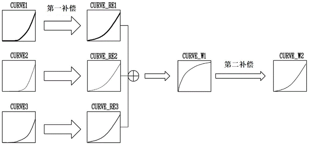
然而,当第一经补偿的伽马曲线CURVE_RE1、第二经补偿的伽马曲线CURVE_RE2和第三经补偿的伽马曲线CURVE_RE3合并为单个白色伽马曲线CURVE_W1时,白色伽马曲线CURVE_W1(或第一像素PX1、第二像素PX2和第三像素PX3的白平衡)可能失真,并且然后可具有与第一经补偿的伽马曲线CURVE_RE1、第二经补偿的伽马曲线CURVE_RE2和第三经补偿的伽马曲线CURVE_RE3的形状不同的形状,即,不同的伽马特性。However, when the first compensated gamma curve CURVE_RE1, the second compensated gamma curve CURVE_RE2, and the third compensated gamma curve CURVE_RE3 are combined into a single white gamma curve CURVE_W1, the white gamma curve CURVE_W1 (or the The white balance of the one pixel PX1, the second pixel PX2, and the third pixel PX3) may be distorted, and may then have the same The shape of the gamma curve CURVE_RE3 is a different shape, ie, a different gamma characteristic.
其原因在于,当第一像素PX1、第二像素PX2和第三像素PX3同时发光时,在第一像素PX1、第二像素PX2和第三像素PX3的每个中发生的横向泄漏减少。The reason for this is that when the first pixel PX1 , the second pixel PX2 and the third pixel PX3 emit light at the same time, the lateral leakage occurring in each of the first pixel PX1 , the second pixel PX2 and the third pixel PX3 is reduced.
因此,图5的第二数据补偿器220可通过对白色伽马曲线CURVE_W1执行第二补偿来将白色伽马曲线CURVE_W1重新调节为经校正的白色伽马曲线CURVE_W2。此处,经校正的白色伽马曲线CURVE_W2可与基准伽马曲线匹配。Therefore, the
在示例性实施方式中,第二数据补偿器220可使用以下等式(2)将目标像素的重新映射的灰度值GRAY_RE校正为经补偿的灰度值GRAY_C:In an exemplary embodiment, the
GRAYij′=GRAYij-G×D(a1×GRAYi-1j-1+a2×GRAYi-1jGRAYij′=GRAYij-G×D(a1×GRAYi-1j-1+a2×GRAYi-1j
+a3×GRAYi-1j+1+a4×GRAYij-1+a5×GRAYij+1+a6×GRAYi+1j-1+a3×GRAYi-
+a7×GRAYi+1j+a8×GRAYi+1j+1) (2)+a7×GRAYi+1j+a8×GRAYi+1j+1) (2)
此处,GRAYij可为与位于第i行和第j列的像素对应的重新映射的灰度值GRAY_RE,并且GRAYij′可为GRAYij的经补偿的灰度值GRAY_C。此处,a1、a2、a3、a4、a5、a6、a7和a8可为相邻灰度值的相应的补偿系数,G可为第一增益,并且D可为第二增益。如稍后将描述的,第一增益G可随着目标像素的重新映射的灰度值GRAY_RE的增大而减小,并且例如,可为0与1之间的值。相似地,第二增益D可随着显示装置1的调光水平的增加而减小,并且例如,可为0与1之间的值。Here, GRAYij may be the remapped grayscale value GRAY_RE corresponding to the pixel located at the ith row and the jth column, and GRAYij' may be the compensated grayscale value GRAY_C of GRAYij. Here, a1, a2, a3, a4, a5, a6, a7, and a8 may be corresponding compensation coefficients of adjacent grayscale values, G may be the first gain, and D may be the second gain. As will be described later, the first gain G may decrease as the remapped grayscale value GRAY_RE of the target pixel increases, and may be a value between 0 and 1, for example. Similarly, the second gain D may decrease as the dimming level of the
例如,位于第二行和第二列中的像素的经补偿的灰度值GRAY_C(即,GRAY22′)可被校正或计算为“GRAY22-G*D*(a1*GRAY11+a2*GRAY12+a3*GRAY13+a4*GRAY21+a5*GRAY23+a6*GRAY31+a7*GRAY32+a8*GRAY33)”。For example, the compensated grayscale value GRAY_C (ie, GRAY22') of the pixels located in the second row and second column may be corrected or calculated as "GRAY22-G*D*(a1*GRAY11+a2*GRAY12+a3" *GRAY13+a4*GRAY21+a5*GRAY23+a6*GRAY31+a7*GRAY32+a8*GRAY33)”.
当使用等式(2)计算的经补偿的灰度值GRAY_C具有负(-)值时,第二数据补偿器220可将经补偿的灰度值GRAY_C替换为0,或者可截断经补偿的灰度值GRAY_C。When the compensated gray value GRAY_C calculated using Equation (2) has a negative (-) value, the
通过等式(2),第二数据补偿器220可通过响应于相邻灰度值中的一个增加而减小目标像素的重新映射的灰度值GRAY_RE来生成经补偿的灰度值GRAY_C。Through equation (2), the
在示例性实施方式中,第二数据补偿器220可基于相邻灰度值来计算目标像素的第一补偿值,并且可通过从目标像素的重新映射的灰度值GRAY_RE减去第一补偿值来计算目标像素的经补偿的灰度值GRAY_C。In an exemplary embodiment, the
在示例性实施方式中,第二数据补偿器220可根据相邻灰度值通过使用相应的预设补偿系数a1至a8作为权重来计算相邻灰度值的加权和,从而计算第一补偿值。此处,补偿系数a1至a8可包括在补偿滤波器中。In an exemplary embodiment, the
补偿滤波器可通过参照图9A和图9B来解释。图9A是示出在图5的控制器中的第二数据补偿器中使用的补偿滤波器的示例的图。图9B是示出图9A的补偿滤波器的实施方式的图。The compensation filter can be explained by referring to FIGS. 9A and 9B . FIG. 9A is a diagram showing an example of a compensation filter used in the second data compensator in the controller of FIG. 5 . FIG. 9B is a diagram illustrating an embodiment of the compensation filter of FIG. 9A .
首先,参照图9A,补偿滤波器FILTER1可具有3行*3列的尺寸,并且可包括第一补偿系数a1、第二补偿系数a2、第三补偿系数a3、第四补偿系数a4、第五补偿系数a5、第六补偿系数a6、第七补偿系数a7和第八补偿系数a8以及基准补偿系数a0。基准补偿系数a0可为待应用于与目标像素对应的重新映射的灰度值GRAY_RE的系数,并且例如,可为0。First, referring to FIG. 9A , the compensation filter FILTER1 may have a size of 3 rows*3 columns, and may include a first compensation coefficient a1, a second compensation coefficient a2, a third compensation coefficient a3, a fourth compensation coefficient a4, a fifth compensation coefficient The coefficient a5, the sixth compensation coefficient a6, the seventh compensation coefficient a7, the eighth compensation coefficient a8, and the reference compensation coefficient a0. The reference compensation coefficient a0 may be a coefficient to be applied to the remapped gray value GRAY_RE corresponding to the target pixel, and may be 0, for example.
在示例性实施方式中,第一补偿系数a1、第二补偿系数a2、第三补偿系数a3、第四补偿系数a4、第五补偿系数a5、第六补偿系数a6、第七补偿系数a7和第八补偿系数a8可分别为0.01与0.15之间的常数,并且第一补偿系数a1至第八补偿系数a8的总和可小于0.5。In the exemplary embodiment, the first compensation coefficient a1, the second compensation coefficient a2, the third compensation coefficient a3, the fourth compensation coefficient a4, the fifth compensation coefficient a5, the sixth compensation coefficient a6, the seventh compensation coefficient a7 and the The eight compensation coefficients a8 may be constants between 0.01 and 0.15, respectively, and the sum of the first compensation coefficient a1 to the eighth compensation coefficient a8 may be less than 0.5.
在示例性实施方式中,在相邻像素之中,包括在与目标像素相同行中的第一相邻像素的第一补偿系数可与包括在与目标像素相同列中的第二相邻像素的第二补偿系数不同。例如,第一补偿系数可大于第二补偿系数。In an exemplary embodiment, among adjacent pixels, a first compensation coefficient of a first adjacent pixel included in the same row as the target pixel may be different from that of a second adjacent pixel included in the same column as the target pixel The second compensation coefficient is different. For example, the first compensation coefficient may be greater than the second compensation coefficient.
参照图9B,示例性地示出了第一补偿滤波器FILTER_S1和第二补偿滤波器FILTER_S2。Referring to FIG. 9B , a first compensation filter FILTER_S1 and a second compensation filter FILTER_S2 are exemplarily shown.
在第一补偿滤波器FILTER_S1中,包括在与目标像素相同行中的第一相邻像素的第一补偿系数,即,图9A中所示的第四补偿系数a4和第五补偿系数a5为0.125。包括在与目标像素相同列中的第二相邻像素的第二补偿系数,即,图9A中所示的第二补偿系数a2和第七补偿系数a7为0.1。此处,第四补偿系数a4和第五补偿系数a5可大于第二补偿系数a2和第七补偿系数a7。In the first compensation filter FILTER_S1, the first compensation coefficient of the first adjacent pixel included in the same row as the target pixel, that is, the fourth compensation coefficient a4 and the fifth compensation coefficient a5 shown in FIG. 9A are 0.125 . The second compensation coefficient of the second adjacent pixel included in the same column as the target pixel, that is, the second compensation coefficient a2 and the seventh compensation coefficient a7 shown in FIG. 9A are 0.1. Here, the fourth compensation coefficient a4 and the fifth compensation coefficient a5 may be larger than the second compensation coefficient a2 and the seventh compensation coefficient a7.
其原因在于,通过上面参考图1描述的栅极驱动器130,显示单元110(或像素PX)以顺序驱动方式显示图像,并因此与包括在相同列中以顺序地发光的相邻像素相比,作用在目标像素上的由包括在相同行中以同时发光的相邻像素的横向泄漏引起的影响更多。The reason for this is that, by the
在相对于目标像素的对角线方向上排列的相邻像素的第一补偿系数a1、第三补偿系数a3、第六补偿系数a6和第八补偿系数a8可远远小于剩余补偿系数a2、a4、a5和a7。其原因在于,取决于像素阵列的结构,在相对于目标像素的对角线方向上排列的相邻像素与目标像素相对地间隔开,并因此横向泄漏的影响可较少地作用在目标像素上。The first compensation coefficient a1, the third compensation coefficient a3, the sixth compensation coefficient a6 and the eighth compensation coefficient a8 of the adjacent pixels arranged in the diagonal direction with respect to the target pixel may be much smaller than the remaining compensation coefficients a2, a4 , a5 and a7. The reason for this is that, depending on the structure of the pixel array, adjacent pixels arranged in a diagonal direction with respect to the target pixel are relatively spaced apart from the target pixel, and thus the influence of lateral leakage can be less exerted on the target pixel. .
相似地,在第二补偿滤波器FILTER_S2中,包括在与目标像素相同行中的第一相邻像素的第一补偿系数,即,图9A中所示的第四补偿系数a4和第五补偿系数a5可为最大值,即0.1。包括在与目标像素相同列中的第二相邻像素的第二补偿系数,即,图9A中所示的第二补偿系数a2和第七补偿系数a7可为0.05。此处,第一补偿系数a1、第三补偿系数a3、第六补偿系数a6和第八补偿系数a8可为最小值,即0.025。Similarly, in the second compensation filter FILTER_S2, the first compensation coefficients of the first adjacent pixels in the same row as the target pixel, that is, the fourth compensation coefficient a4 and the fifth compensation coefficient shown in FIG. 9A are included a5 can be the maximum value, ie 0.1. The second compensation coefficient of the second adjacent pixel included in the same column as the target pixel, that is, the second compensation coefficient a2 and the seventh compensation coefficient a7 shown in FIG. 9A may be 0.05. Here, the first compensation coefficient a1, the third compensation coefficient a3, the sixth compensation coefficient a6 and the eighth compensation coefficient a8 may be the minimum value, that is, 0.025.
在示例性实施方式中,第二数据补偿器220可以以像素为基础在移动补偿滤波器(例如,第一补偿滤波器FILTER_S1或第二补偿滤波器FILTER_S2)的同时持续地计算补偿滤波器中的第一补偿值或经补偿的灰度值GRAY_C。In an exemplary embodiment, the
计算第二数据补偿器220的经补偿的灰度值GRAY_C的过程可参照图10来解释。图10是示出图5的控制器使用图9A的补偿滤波器来补偿灰度值的处理的示例的图。The process of calculating the compensated gray value GRAY_C of the
参照图1、图9A和图10,示例性地示出了图1的第一区域A1中的像素PX,其中,像素PX可以以RGBG pentile结构布置。1 , 9A and 10 , the pixels PX in the first area A1 of FIG. 1 are exemplarily shown, wherein the pixels PX may be arranged in an RGBG pentile structure.
在第一步骤STEP1处,第二数据补偿器220可根据第21绿色像素G21排列补偿滤波器FILTER1,在补偿滤波器FILTER1中计算与第11红色像素R11、第11绿色像素G11、第12蓝色像素B12、第21蓝色像素B21、第22红色像素R22、第31红色像素R31、第31绿色像素G31和第32蓝色像素B32对应的灰度值的加权和,且然后计算与第21绿色像素G21对应的补偿值或经补偿的灰度值GRAY_C。At the first step STEP1, the
作为参考,第二数据补偿器220可仅考虑像素阵列而不考虑像素的发射颜色来计算补偿值或经补偿的灰度值GRAY_C。相应地,发射与目标像素(例如,第21绿色像素G21)的颜色不同颜色的光的至少一个像素(例如,第11红色像素R11、第12蓝色像素B12等)的灰度值可用于计算目标像素的补偿值或第二经补偿的灰度值。For reference, the
相似地,在第二步骤STEP2处,第二数据补偿器220可根据第22红色像素R22移动或排列补偿滤波器FILTER1,在补偿滤波器FILTER1中计算与相邻像素对应的灰度值的加权和,且然后计算与第22红色像素R22对应的补偿值或第二经补偿的灰度值。Similarly, at the second step STEP2, the
在第三步骤STEP3处,当完成针对一行的补偿值或第二经补偿的灰度值的计算时,第二数据补偿器220可根据下一行中的第31绿色像素G31来排列补偿滤波器FILTER1,且然后计算与第31绿色像素G31对应的补偿值或第二经补偿的灰度值。At the third step STEP3, when the calculation of the compensation value or the second compensated grayscale value for one row is completed, the
此后,在第四步骤STEP4处,第二数据补偿器220可以以像素为基础在行方向(或水平方向)上移动补偿滤波器FILTER1的同时重复执行补偿值或第二经补偿的灰度值。Thereafter, at the fourth step STEP4, the
在示例性实施方式中,第二数据补偿器220可通过选择性地应用多个补偿滤波器来计算补偿值或经补偿的灰度值GRAY_C。In an exemplary embodiment, the
选择性地应用补偿滤波器的配置可参照图11来解释。图11是示出图5的控制器使用图9A的补偿滤波器来补偿灰度值的处理的示例的图。The configuration for selectively applying the compensation filter can be explained with reference to FIG. 11 . FIG. 11 is a diagram illustrating an example of a process in which the controller of FIG. 5 uses the compensation filter of FIG. 9A to compensate gradation values.
参照图10和图11,在第一步骤STEP1至第四步骤STEP4处,第二数据补偿器220的操作与图10的第二数据补偿器220的操作的不同之处在于,选择性地应用对像素的相应类型(或相应发射颜色)设置的绿色滤波器FILTER_G、红色滤波器FILTER_R和蓝色滤波器FILTER_B。例如,绿色滤波器FILTER_G可为图9B中所示的第一补偿滤波器FILTER_S1、红色滤波器FILTER_R和蓝色滤波器FILTER_B可分别是图9B中所示的第二补偿滤波器FILTER_S2,但是补偿滤波器的应用不限于此。10 and 11 , at the first step STEP1 to the fourth step STEP4 , the operation of the
如图11中所示,在第一步骤STEP1处,第二数据补偿器220可将绿色滤波器FILTER_G应用到第21绿色像素G21。在第二步骤STEP2处,第二数据补偿器220可将红色滤波器FILTER_R应用到第22红色像素R22。在第三步骤STEP3处,第二数据补偿器220可将绿色滤波器FILTER_G应用到第31绿色像素G31。在第四步骤STEP4处,第二数据补偿器220可将蓝色滤波器FILTER_B应用到第32蓝色像素B32。As shown in FIG. 11, at the first step STEP1, the
即,第二数据补偿器220可通过将不同的滤波器(例如,绿色滤波器FILTER_G、红色滤波器FILTER_R和蓝色滤波器FILTER_B)中的一个选择性地应用到每个相邻像素来计算补偿值或经补偿的灰度值GRAY_C。That is, the
在示例性实施方式中,在等式(2)中使用的第一增益G可基于目标像素的第一经补偿的灰度值来设置,可随着第一经补偿的灰度值增加而减小,并且可具有范围在约从0至1的值。In an exemplary embodiment, the first gain G used in equation (2) may be set based on the first compensated grayscale value of the target pixel, and may decrease as the first compensated grayscale value increases is small, and can have values ranging from about 0 to 1.
第一增益G可参照图12来解释。图12是示出在图5的控制器中使用的第一增益的示例的曲线图。The first gain G can be explained with reference to FIG. 12 . FIG. 12 is a graph showing an example of a first gain used in the controller of FIG. 5 .
参照图12,当重新映射的灰度值GRAY_RE等于第二灰度范围的起始灰度值GRAY_START时,第一增益G(或全局增益)可具有最大值(例如,1),并且当重新映射的灰度值GRAY_RE等于第二灰度范围的最终灰度值GRAY_END时,第一增益G(或全局增益)可具有最小值(例如,0)。Referring to FIG. 12 , when the remapped gray value GRAY_RE is equal to the starting gray value GRAY_START of the second gray range, the first gain G (or global gain) may have a maximum value (eg, 1), and when the remapped gray value GRAY_RE When the grayscale value GRAY_RE of GRAY_RE is equal to the final grayscale value GRAY_END of the second grayscale range, the first gain G (or the global gain) may have a minimum value (eg, 0).
参照图6作为示例,当重新映射的灰度值GRAY_RE是14时,第一增益G可具有1的值,并且当重新映射的灰度值GRAY_RE是32时,第一增益G可具有0的值。Referring to FIG. 6 as an example, when the remapped gray value GRAY_RE is 14, the first gain G may have a value of 1, and when the remapped gray value GRAY_RE is 32, the first gain G may have a value of 0 .
当重新映射的灰度值GRAY_RE在第二灰度范围内增加时,第一增益G线性地减小。当重新映射的灰度值GRAY_RE大于第二灰度范围的最终灰度值GRAY_END时,第一增益G可具有最小值,例如,0的值。The first gain G decreases linearly when the remapped gray value GRAY_RE increases within the second gray range. When the remapped gray value GRAY_RE is greater than the final gray value GRAY_END of the second gray range, the first gain G may have a minimum value, eg, a value of 0.
如上面参考图3和图4所描述的,重新映射的灰度值GRAY_RE减小,对于目标像素的横向泄漏可增加,并且相邻像素的影响也可增加。因此,在等式(2)中,补偿值(即,与相邻像素对应的相邻灰度值的加权和)与重新映射的灰度值GRAY_RE成反比。随着目标像素的重新映射的灰度值GRAY_RE越小,相邻灰度值的影响可能更多作用在目标像素上。As described above with reference to FIGS. 3 and 4 , the remapped gray value GRAY_RE decreases, the lateral leakage to the target pixel can increase, and the influence of adjacent pixels can also increase. Therefore, in equation (2), the compensation value (ie, the weighted sum of adjacent gray values corresponding to adjacent pixels) is inversely proportional to the remapped gray value GRAY_RE. As the remapped gray value GRAY_RE of the target pixel is smaller, the influence of adjacent gray values may act more on the target pixel.
在示例性实施方式中,在等式(2)中使用的第二增益D可基于显示装置1的调光水平来设置,可随着调光水平变高而减小,并且可具有范围在从0至1的值。In an exemplary embodiment, the second gain D used in Equation (2) may be set based on the dimming level of the
第二增益D可参照图13来解释。图13是示出在图5的控制器中使用的第二增益的示例的曲线图。The second gain D can be explained with reference to FIG. 13 . FIG. 13 is a graph showing an example of a second gain used in the controller of FIG. 5 .
参照图13,第二增益D(或调光增益)可在最小调光水平DIM_MIN处具有最大值(最大调光增益:Max Dimming Gain,例如,1),可在最大调光水平为DIM_MAX处具有最小值(最小调光增益:Min Dimming Gain,例如,0),并且可随着调光水平增加而线性地减小。参照图4作为示例,当调光水平为25%时,第二增益D可具有1的值,并且当调光水平是100%时,第二增益D可具有0.1的值。Referring to FIG. 13 , the second gain D (or dimming gain) may have a maximum value at the minimum dimming level DIM_MIN (maximum dimming gain: Max Dimming Gain, eg, 1), and may have a maximum dimming level at DIM_MAX The minimum value (minimum dimming gain: Min Dimming Gain, eg, 0), and may decrease linearly as the dimming level increases. Referring to FIG. 4 as an example, when the dimming level is 25%, the second gain D may have a value of 1, and when the dimming level is 100%, the second gain D may have a value of 0.1.
其原因在于,如上面参考图3和图4所描述的,随着调光水平变低,所有的第一经补偿的灰度值可变小,并因此对于目标像素的横向泄漏可相对增加,并且相邻像素的影响可增加。The reason for this is that, as described above with reference to FIGS. 3 and 4 , as the dimming level becomes lower, all the first compensated grayscale values may become smaller, and thus the lateral leakage to the target pixel may relatively increase, And the influence of adjacent pixels may increase.
因此,在等式(2)中,补偿值(即,与相邻像素对应的相邻灰度值的加权和)与调光水平成反比。随着调光水平变低,相邻灰度值的影响可能更多作用在目标像素上。Therefore, in equation (2), the compensation value (ie, the weighted sum of adjacent grayscale values corresponding to adjacent pixels) is inversely proportional to the dimming level. As the dimming level becomes lower, the influence of adjacent gray values may act more on the target pixel.
如上面参考图5、图6、图7、图8、图9A、图9B、图10、图11、图12和图13所描述的,数据转换器200(或控制器140)可校正相应的像素的伽马特性,以使得伽马特性通过灰度重新映射在低灰度范围(或低电流区或低亮度区)中与基准伽马特性匹配。而且,数据转换器200可校正由像素引起的白色伽马特性(或白平衡),以使得白色伽马特性通过使用相邻灰度值的灰度补偿来与基准伽马特性匹配。因此,可防止或减少显示装置1的显示品质的劣化。As described above with reference to FIGS. 5, 6, 7, 8, 9A, 9B, 10, 11, 12, and 13, the data converter 200 (or the controller 140) may correct the corresponding The gamma characteristic of the pixel such that the gamma characteristic matches the reference gamma characteristic in the low grayscale range (or low current region or low brightness region) by grayscale remapping. Also, the
与此同时,在图5和图13中,已经描述了第二数据补偿器220基于重新映射的灰度值GRAY_RE和相邻灰度值(或相邻像素的重新映射的灰度值)来补偿重新映射的灰度值GRAY_RE并且生成经补偿的灰度值GRAY_C的示例,但是本公开不限于此。Meanwhile, in FIGS. 5 and 13 , it has been described that the
在实施方式中,第二数据补偿器220可基于重新映射的灰度值GRAY_RE和相邻灰度值(或相邻像素的重新映射的灰度值)来补偿输入灰度值GRAY_IN,且然后可生成经补偿的灰度值GRAY_C(或第二经补偿的灰度值)。In an embodiment, the
在实施方式中,第二数据补偿器220可使用以下等式(3)将目标像素的输入灰度值GRAY_IN校正为经补偿的灰度值GRAY_C。In an embodiment, the
(1)GRAYij′=GRAY_INij+F(Δij-LLF(i,j))(1) GRAYij'=GRAY_INij+F(Δij-LLF(i,j))
(but,F(X)=x(x>0),0(x<0))(but, F(X)=x(x>0), 0(x<0))
(2)Δij=GRAYij-GRAY_INij(2) Δij=GRAYij-GRAY_INij
(3)LLF(i,j)=G×D×(a1×GRAYi-1j-1+a2×GRAYi-1j+a3×GRAYi-1j+1+a4×GRAYij-1+a0×GRAYij+a5×GRAYij+1+a6×GRAYi+1j-1+a7×GRAYi+1j+a8×GRAYi+1j+1)(3)(3) LLF(i, j)=G×D×(a1×GRAYi-1j-1+a2×GRAYi-1j+a3×GRAYi-
此处,GRAY_INij可为与位于第i行和第j列的像素对应的输入灰度值GRAY_IN,GRAYij可为输入灰度值GRAY_IN的重新映射的灰度值GRAY_RE,并且GRAYij′可为输入灰度值GRAY_IN的经补偿的灰度值GRAY_C。Δij可为重新映射的灰度值GRAY_RE与输入灰度值GRAY_IN之间的差值。a0可为输入灰度值GRAY_IN的基准补偿系数,a1至a8可为相邻灰度值的相应的补偿系数,G可为第一增益,并且D可为第二增益。如稍后将描述的,第一增益G可随着目标像素的重新映射的灰度值GRAY_RE的增大而减小,并且例如,可为0与1之间的值。相似地,第二增益D可随着显示装置1的调光水平的增加而减小,并且例如,可为0与1之间的值。F(x)可为x的极限函数。Here, GRAY_INij may be the input gray value GRAY_IN corresponding to the pixel located at row i and column j, GRAYij may be the remapped gray value GRAY_RE of the input gray value GRAY_IN, and GRAYij′ may be the input gray value The compensated grayscale value GRAY_C of the value GRAY_IN. Δij may be the difference between the remapped gray value GRAY_RE and the input gray value GRAY_IN. a0 may be the reference compensation coefficient of the input gray value GRAY_IN, a1 to a8 may be the corresponding compensation coefficients of the adjacent gray values, G may be the first gain, and D may be the second gain. As will be described later, the first gain G may decrease as the remapped grayscale value GRAY_RE of the target pixel increases, and may be a value between 0 and 1, for example. Similarly, the second gain D may decrease as the dimming level of the
例如,位于第二行和第二列中的像素的经补偿的灰度值GRAY_C(即,GRAY22′)可计算为“GRAY_IN22+F(GRAY22-GRAY_IN22)-G*D*(a1*GRAY11+a2*GRAY12+a3*GRAY13+a4*GRAY21+a5*GRAY23+a6*GRAY31+a7*GRAY32+a8*GRAY33)”。For example, the compensated grayscale value GRAY_C (ie, GRAY22') of the pixels located in the second row and second column may be calculated as "GRAY_IN22+F(GRAY22-GRAY_IN22)-G*D*(a1*GRAY11+a2) *GRAY12+a3*GRAY13+a4*GRAY21+a5*GRAY23+a6*GRAY31+a7*GRAY32+a8*GRAY33)”.
与此同时,根据情况,目标像素的输入灰度值GRAY_IN可重新映射为低于输入灰度值GRAY_IN的灰度值。相应地,等式(3)可由以下等式(4)概括并表示:Meanwhile, according to circumstances, the input gray value GRAY_IN of the target pixel may be remapped to a gray value lower than the input gray value GRAY_IN. Accordingly, equation (3) can be summarized and represented by the following equation (4):
GRAYij′=GRAY_INij+(sign ofΔij)×(F(|Δij|-LLF(i,j))GRAYij'=GRAY_INij+(sign ofΔij)×(F(|Δij|-LLF(i,j))
(but,F(x)=x(x>0),o(x<0),and(but, F(x)=x(x>0), o(x<0), and
sign ofΔij=1(Δij>0),-1(Δij<0))sign ofΔij=1 (Δij>0), -1 (Δij<0))
(4) (4)
此处,Δij的符号可为差值的符号,并且|Δij|可为Δij的绝对值。Here, the sign of Δij may be the sign of the difference, and |Δij| may be the absolute value of Δij.
基于等式(4)的补偿输入灰度值GRAY_IN的第二数据补偿器220可实现为基于图14的框图的逻辑电路。The
图14是示出包括在图5的控制器中的第二数据补偿器的示例的框图。FIG. 14 is a block diagram illustrating an example of a second data compensator included in the controller of FIG. 5 .
参照图14,第二数据补偿器220可包括第一运算电路1410(或第一逻辑运算电路)、第二运算电路1420、第三运算电路1430、第四运算电路1440和第五运算电路1450。14 , the
第一运算电路1410可通过从由第一数据补偿器210生成的目标像素的重新映射的灰度值GRAY_RE减去目标像素的输入灰度值GRAY_IN来计算差值Δ。The
第二运算电路1420可基于相邻灰度值来计算目标像素的第一补偿值C_GRAY1。例如,第二运算电路1420可使用补偿滤波器(或横向泄漏滤波器:LLF)来计算第一补偿值C_GRAY1,并且稍后将参考图10对其进行描述。The
第三运算电路1430可通过从差值的绝对值|Δ|减去第一补偿值C_GRAY1来计算第二补偿值C_GRAY2。The
第四运算电路1440可通过将差值的符号(即,Δ的符号)乘以第二补偿值C_GRAY2来设置第二补偿值C_GRAY2的符号。The
第五运算电路1450可通过将输入灰度值GRAY_IN与第二补偿值C_GRAY2相加来计算经补偿的灰度值GRAY_C。作为参考,当通过补偿重新映射的灰度值GRAY_RE来生成经补偿的灰度值时,经补偿的灰度值可低于输入灰度值GRAY_IN,并因此第二数据补偿器220可补偿输入灰度值GRAY_IN,而不是重新映射的灰度值GRAY_RE。The
与此同时,尽管已将第二数据补偿器220描述为使用图14中的等式(4)(或等式(3))计算经补偿的灰度值GRAY_C,但是本公开不限于此。Meanwhile, although the
在实施方式中,第二数据补偿器220可使用以下等式(5)将目标像素的输入灰度值GRAY_IN校正为经补偿的灰度值GRAY_C。In an embodiment, the
(1)GRAYij′=GRAY_INij+F(Δij-LLF(i,j))×GAIN(1) GRAYij′=GRAY_INij+F(Δij-LLF(i,j))×GAIN
(2)Δij=GRAYij-GRAY_INij(2) Δij=GRAYij-GRAY_INij
(3)LLF(i,j)=G×D×(a1×GRAYi-1j-1+a2×GRAYi-1j+a3×GRAYi-1j+1+a4×GRAYij-1+a0×GRAYij+a5×GRAYij+1+a6×GRAYi+1j-1+a7×GRAYi+1j+a8×GRAYi+1j+1)+a(but,a≠0)(3) LLF(i, j)=G×D×(a1×GRAYi-1j-1+a2×GRAYi-1j+a3×GRAYi-
(4)GAIN=GRAY_INij/LLF(i,j) (5)(4) GAIN=GRAY_INij/LLF(i, j) (5)
基于等式(5)的经补偿的灰度值GRAY_C(即,GRAYij′)可与基于等式(2)的经补偿的灰度值不同之处在于GRAYij′是考虑增益来计算的。The compensated grayscale value GRAY_C (ie, GRAYij') based on equation (5) may be different from the compensated grayscale value based on equation (2) in that GRAYij' is calculated considering the gain.
基于等式(5)的补偿输入灰度值GRAY_IN的第二数据补偿器220可实现为基于图15的框图的逻辑电路。The
图15是示出包括在图5的控制器中的第二数据补偿器的示例的框图。FIG. 15 is a block diagram illustrating an example of a second data compensator included in the controller of FIG. 5 .
参照图14和图15,图15的第二数据补偿器2201可包括第一运算电路1510(或第一逻辑运算电路)、第二运算电路1520、第三运算电路1530、第四运算电路1540、第五运算电路1550和第六运算电路1560。由于第一运算电路1510、第二运算电路1520、第三运算电路1530、第四运算电路1540和第五运算电路1550与上面参考图14描述的第一运算电路1410(或第一逻辑运算电路)、第二运算电路1420、第三运算电路1430、第四运算电路1440和第五运算电路1450基本上一致或相似,其重复描述将被省略。14 and 15 , the second data compensator 2201 of FIG. 15 may include a first operation circuit 1510 (or a first logic operation circuit), a
第三运算电路1530可通过从差值Δ减去第一补偿值C_GRAY1来计算第二补偿值C_GRAY2。The
第六运算电路1560可通过将输入灰度值GRAY_IN除以第一补偿值C_GRAY1来计算增益。The
第四运算电路1540可通过将第二补偿值C_GRAY2乘以增益来计算第三补偿值C_GRAY3。The
第五运算电路1550可通过将输入灰度值GRAY_IN与第三补偿值C_GRAY3相加来计算经补偿的灰度值GRAY_C。The
为了描述由图15的第二数据补偿器220_1获得的效果,下面可参照图16A和图16B。In order to describe the effect obtained by the second data compensator 220_1 of FIG. 15 , reference may be made to FIGS. 16A and 16B below.
图16A是示出由图15的第二数据补偿器为白色图像计算的补偿值的图,并且图16B是示出由图15的第二数据补偿器为单色图像计算的补偿值的图。16A is a diagram showing compensation values calculated by the second data compensator of FIG. 15 for a white image, and FIG. 16B is a diagram showing compensation values calculated by the second data compensator of FIG. 15 for a monochrome image.
参照图15、图16A和图16B,差值曲线CURVE_D指示灰度值之间的差值Δ(即,重新映射的灰度值与输入灰度值之间的差异),第一补偿值曲线CURVE_LLF指示取决于灰度值的第一补偿值C_GRAY1(即,通过应用补偿滤波器计算的补偿值),并且第二补偿值曲线CURVE_F指示取决于灰度值的第二补偿值C_GRAY2(即,对差值Δ与第一补偿值C_GRAY1之间的差异应用极限函数的结果)。第三补偿值曲线CURVE_C指示第三补偿值C_GRAY3(即,通过将增益乘以第二补偿值C_GRAY2而获得的值)。此处,图16A中所示的第三补偿值曲线CURVE_C表示用于白色图像的第三补偿值C_GRAY3,并且图16B中所示的第三补偿值曲线CURVE_C表示用于单色图像的第三补偿值C_GRAY3。15 , 16A and 16B , the difference value curve CURVE_D indicates the difference value Δ between gray values (ie, the difference between the remapped gray value and the input gray value), the first compensation value curve CURVE_LLF A first compensation value C_GRAY1 (ie, a compensation value calculated by applying a compensation filter) is indicated, and the second compensation value curve CURVE_F is a second compensation value C_GRAY2 (ie, a differential value) that is dependent on a gray value. The difference between the value Δ and the first compensation value C_GRAY1 is the result of applying the limit function). The third compensation value curve CURVE_C indicates the third compensation value C_GRAY3 (ie, a value obtained by multiplying the gain by the second compensation value C_GRAY2). Here, the third compensation value curve CURVE_C shown in FIG. 16A represents the third compensation value C_GRAY3 for the white image, and the third compensation value curve CURVE_C shown in FIG. 16B represents the third compensation for the monochrome image Value C_GRAY3.
当第二数据补偿器220_1使用在上面参考图9描述的等式(4)或等式(2)时,可通过将第二补偿值C_GRAY2与输入灰度值GRAY_IN相加来计算经补偿的灰度值GRAY_C。When the second data compensator 220_1 uses Equation (4) or Equation (2) described above with reference to FIG. 9 , the compensated gray scale may be calculated by adding the second compensation value C_GRAY2 to the input gray scale value GRAY_IN Degree value GRAY_C.
如上面参考图3所描述的,尽管由白色图像引起的横向泄漏不会以很大的水平发生,但是如图16A中所示,第二补偿值C_GRAY2可具有相对大的值,因此对输入灰度值GRAY_IN进行了过度补偿。As described above with reference to FIG. 3 , although the lateral leakage caused by the white image does not occur at a large level, as shown in FIG. 16A , the second compensation value C_GRAY2 may have a relatively large value, so that the input gray The degree value GRAY_IN is overcompensated.
根据本公开的实施方式的第二数据补偿器220_1可通过使用在上面参考图15描述的等式(4)将反映了增益的第三补偿值C_GRAY3与输入灰度值GRAY_IN相加来计算经补偿的灰度值GRAY_C。如图16A中所示,由于增益(即,输入灰度值与第一补偿值C_GRAY1的比例)相对于白色图像(与其它图像相比)具有相对小的值,因此第三补偿值C_GRAY3可具有相对小的值,并因此可防止对输入灰度值GRAY_IN的过度补偿。The second data compensator 220_1 according to an embodiment of the present disclosure may calculate the compensated by adding the third compensation value C_GRAY3 reflecting the gain to the input grayscale value GRAY_IN using Equation (4) described above with reference to FIG. 15 . The gray value of GRAY_C. As shown in FIG. 16A , since the gain (ie, the ratio of the input gray value to the first compensation value C_GRAY1 ) has a relatively small value with respect to the white image (compared to other images), the third compensation value C_GRAY3 may have A relatively small value, and thus prevents overcompensation of the input gray value GRAY_IN.
与此同时,取决于单色图像的横向泄漏可能以相对大的水平发生。在这种情况下,如图16B中所示,由于增益(即,输入灰度值与第一补偿值C_GRAY1的比例)相对于单色图像(与白色图像相比)具有相对大的值,因此第三补偿值C_GRAY3可具有相对大的值(例如,与第二补偿值C_GRAY2相似的值),因此能够使得输入灰度值GRAY_IN被充分地补偿。At the same time, lateral leakage depending on a monochrome image may occur at a relatively large level. In this case, as shown in FIG. 16B , since the gain (ie, the ratio of the input grayscale value to the first compensation value C_GRAY1 ) has a relatively large value with respect to the monochrome image (compared to the white image), therefore The third compensation value C_GRAY3 may have a relatively large value (eg, a value similar to the second compensation value C_GRAY2 ), thus enabling the input grayscale value GRAY_IN to be sufficiently compensated.
如上面参考图15至图16B所描述的,根据本公开的实施方式的第二数据补偿器2201可响应于横向泄漏中的变化而改变补偿值(即,第三补偿值C_GRAY3作为最终反映在输入灰度值GRAY_IN中的补偿值),因此防止显示品质的劣化。As described above with reference to FIGS. 15 to 16B , the second data compensator 2201 according to an embodiment of the present disclosure may change the compensation value (ie, the third compensation value C_GRAY3 as finally reflected in the input) in response to changes in lateral leakage Compensation value in gray value GRAY_IN), thus preventing deterioration of display quality.
图17是示出提供给图5的控制器的测试数据的示例的图。在图17中,以时间顺序描绘了包括在显示单元110中的单个行中的像素的多条线数据DATA_L1至DATA_L4。FIG. 17 is a diagram showing an example of test data provided to the controller of FIG. 5 . In FIG. 17 , a plurality of line data DATA_L1 to DATA_L4 of pixels included in a single row in the
参照图1和图17,可通过图1中所示的数据线DL1至DLm将与多条线数据DATA_L1至DATA_L4对应的数据信号提供给显示单元110。1 and 17 , data signals corresponding to a plurality of line data DATA_L1 to DATA_L4 may be supplied to the
多条线数据DATA_L1至DATA_L4中的每个可包括以每三个数据线重复的数据值。因此,多条线数据DATA_L1至DATA_L4将基于第一数据线DL1至第三数据线DL3来描述。Each of the plurality of line data DATA_L1 to DATA_L4 may include data values repeated every three data lines. Therefore, a plurality of line data DATA_L1 to DATA_L4 will be described based on the first to third data lines DL1 to DL3.
线数据DATA_L1至DATA_L4可根据第二数据线DL2而具有测试值TEST,并且可根据第一数据线DL1和第三数据线DL3而具有最小灰度值MIN或最大灰度值MAX。例如,测试值TEST可为上面参考图6描述的包括在第二低灰度范围内的任意灰度值,并且可具有例如15的灰度值。例如,最小灰度值MIN可为0的灰度值,并且最大灰度值MAX可为255的灰度值。The line data DATA_L1 to DATA_L4 may have a test value TEST according to the second data line DL2, and may have a minimum grayscale value MIN or a maximum grayscale value MAX according to the first and third data lines DL1 and DL3. For example, the test value TEST may be any gray value included in the second low gray scale range described above with reference to FIG. 6 , and may have a gray value of 15, for example. For example, the minimum grayscale value MIN may be a grayscale value of 0, and the maximum grayscale value MAX may be a grayscale value of 255.
根据第一数据线DL1和第三数据线DL3,第一线数据DATA_L1可具有最大灰度值MAX。第二线数据DATA_L2可根据第一数据线DL1而具有最小灰度值MIN,并且可根据第三数据线DL3而具有最大灰度值MAX。第三线数据DATA_L3可根据第一数据线DL1具有最大灰度值MAX,并且可根据第三数据线DL3而具有最小灰度值MIN。第四线数据DATA_L4可与第一线数据DATA_L1相同。According to the first data line DL1 and the third data line DL3, the first line data DATA_L1 may have a maximum grayscale value MAX. The second line data DATA_L2 may have a minimum grayscale value MIN according to the first data line DL1, and may have a maximum grayscale value MAX according to the third data line DL3. The third line data DATA_L3 may have a maximum grayscale value MAX according to the first data line DL1, and may have a minimum grayscale value MIN according to the third data line DL3. The fourth line data DATA_L4 may be the same as the first line data DATA_L1.
显示装置1(或控制器140)可使用相邻像素的相邻灰度值来补偿目标像素的灰度值。相应地,与第二数据线DL2对应的灰度值(或经补偿的灰度值GRAY_C)取决于与第一数据线DL1和第三数据线DL3对应的灰度值的变化而改变,因此能够检查包括在第二数据线DL2中的像素的亮度中的变化。The display device 1 (or the controller 140 ) may use the adjacent grayscale values of the adjacent pixels to compensate the grayscale value of the target pixel. Accordingly, the grayscale value (or the compensated grayscale value GRAY_C) corresponding to the second data line DL2 is changed depending on the change of the grayscale values corresponding to the first data line DL1 and the third data line DL3, so it is possible to Changes in luminance of pixels included in the second data line DL2 are checked.
与此同时,尽管在图17中已将分别与第一线数据DATA_L1至第四线数据DATA_L4对应的数据信号描述为被提供到显示单元110,但是本公开不限于此。Meanwhile, although the data signals respectively corresponding to the first to fourth line data DATA_L1 to DATA_L4 have been described as being supplied to the
例如,第一线数据DATA_L1和第二线数据DATA_L2可彼此组合,以使得与第一数据线DL1(以及第四数据线DL4和第七数据线DL7)对应的灰度值可在从最大灰度值MAX(或具体灰度值,例如,30的灰度值)到最小灰度值MIN的范围内阶段性地改变。而且,与第三数据线DL3(以及第六数据线DL6和第九数据线DL9)对应的灰度值也可阶段性地改变。即,测试数据可对应于灰度图像。For example, the first line data DATA_L1 and the second line data DATA_L2 may be combined with each other so that the grayscale values corresponding to the first data line DL1 (and the fourth and seventh data lines DL4 and DL7 ) may vary from the maximum grayscale value The range from MAX (or a specific gray value, eg, a gray value of 30) to a minimum gray value MIN is changed in stages. Also, the grayscale values corresponding to the third data line DL3 (and the sixth data line DL6 and the ninth data line DL9 ) may also be changed in stages. That is, the test data may correspond to a grayscale image.
图18是示出图5的控制器使用图9A的补偿滤波器来补偿灰度值的处理的示例的图。在图18中示例性地示出了图1的第一区域A1中的像素PX,其中,像素PX可以条纹结构排列。FIG. 18 is a diagram illustrating an example of a process in which the controller of FIG. 5 uses the compensation filter of FIG. 9A to compensate gradation values. Pixels PX in the first area A1 of FIG. 1 are exemplarily shown in FIG. 18 , wherein the pixels PX may be arranged in a stripe structure.
参照图10和图18,图18的像素与具有图10中所示的RGBG pentile结构的像素的不同之处在于图18中所示的像素具有RGB条纹结构。Referring to FIGS. 10 and 18 , the pixel of FIG. 18 is different from the pixel having the RGBG pentile structure shown in FIG. 10 in that the pixel shown in FIG. 18 has the RGB stripe structure.
如上面参考图10所描述的,在第一步骤STEP1至第三步骤STEP3处,控制器140(或图5的数据转换器200)可以以像素为基础在移动上面参考图9A所描述的补偿滤波器FILTER1的同时重复地执行补偿值或经补偿的灰度值GRAY_C的计算。As described above with reference to FIG. 10 , at the first step STEP1 to the third step STEP3 , the controller 140 (or the
即,无论显示单元110中的像素的阵列结构如何,显示装置1均可对输入图像数据执行灰度补偿。That is, regardless of the array structure of the pixels in the
图19是示出包括在图5的控制器中的第二数据补偿器中使用的补偿滤波器的各种示例的图。FIG. 19 is a diagram showing various examples of compensation filters used in the second data compensator included in the controller of FIG. 5 .
参照图19,第一线补偿滤波器FILTER_L1与上面参考图9A等描述的补偿滤波器FILTER1的不同之处在于第一线补偿滤波器FILTER_L1具有1行*3列的尺寸。19 , the first line compensation filter FILTER_L1 is different from the compensation filter FILTER1 described above with reference to FIG. 9A and the like in that the first line compensation filter FILTER_L1 has a size of 1 row*3 columns.
在第一线补偿滤波器FILTER_L1中,可减小用于存储相邻像素的相邻灰度值的线存储器的大小,或者替代性地,可去除线存储器。In the first line compensation filter FILTER_L1, the size of the line memory for storing adjacent grayscale values of adjacent pixels may be reduced, or alternatively, the line memory may be removed.
当第二数据补偿器220或220_1使用第一线补偿滤波器FILTER_L1时,可使用以下等式(6)来计算包括在等式(3)、等式(4)和等式(5)中的LLF(i,j)。When the
LLF(i,j)=c1×GRAYij-1+c0×GRAYij+c2×GRAYij+1+a (6)LLF(i, j)=c1×GRAYij-1+c0×GRAYij+c2×GRAYij+1+a (6)
此处,c0可为用于输入灰度值GRAY_IN的基准补偿系数,并且c1和c2可为相邻灰度值的相应补偿系数。Here, c0 may be a reference compensation coefficient for the input gray value GRAY_IN, and c1 and c2 may be corresponding compensation coefficients of adjacent gray values.
与此同时,第二线补偿滤波器FILTER_L2可具有1行*5列的尺寸。Meanwhile, the second line compensation filter FILTER_L2 may have a size of 1 row*5 columns.
当第二数据补偿器220或220_1使用第二线补偿滤波器FILTER_L2时,可使用以下等式(7)来计算包括在等式(3)、等式(4)和等式(5)中的LLF(i,j)。When the
LLF(i,j)=d1×GRAYij-2+d2×GRAYij-1+d0×GRAYij+d3×GRAYij+1+d4×GRAYij+2+a (7)LLF(i, j)=d1×GRAYij-2+d2×GRAYij-1+d0×GRAYij+d3×GRAYij+1+d4×GRAYij+2+a (7)
此处,d0可为用于输入灰度值GRAY_IN的基准补偿系数,并且d1至d4可为相邻灰度值的相应补偿系数。Here, d0 may be a reference compensation coefficient for the input gray value GRAY_IN, and d1 to d4 may be corresponding compensation coefficients of adjacent gray values.
与此同时,第三线补偿滤波器FILTER_L3可具有1行*6列的尺寸。Meanwhile, the third line compensation filter FILTER_L3 may have a size of 1 row*6 columns.
当第二数据补偿器220或220_1使用第三线补偿滤波器FILTER_L3时,可使用以下等式(8)来计算包括在等式(3)、等式(4)和等式(5)中的LLF(i,j)。When the
LLF(i,j)=e1×GRAYij-3+e2×GRAYij-2+e3×GRAYij-1+e0×GRAYij+e4×GRAYij+1+e5×GRAYij+2+a (8)LLF(i, j)=e1×GRAYij-3+e2×GRAYij-2+e3×GRAYij-1+e0×GRAYij+e4×GRAYij+1+e5×GRAYij+2+a (8)
此处,e0可为用于输入灰度值GRAY_IN的基准补偿系数,并且e1至e5可为相邻灰度值的相应补偿系数。Here, e0 may be a reference compensation coefficient for the input gray value GRAY_IN, and e1 to e5 may be corresponding compensation coefficients of adjacent gray values.
如上面参考图19所描述的,补偿滤波器可被实现为与一行对应的1行*k列-线补偿滤波器(即,第一线补偿滤波器FILTER_L1、第二线补偿滤波器FILTER_L2和第三线补偿滤波器FILTER_L3中的一个),并且线补偿滤波器的尺寸可以以各种形式改变,其中,k可为例如等于或大于3的值。As described above with reference to FIG. 19 , the compensation filters may be implemented as 1 row*k columns-line compensation filters corresponding to one row (ie, the first line compensation filter FILTER_L1, the second line compensation filter FILTER_L2, and the third line compensation filter FILTER_L2). One of the compensation filters FILTER_L3), and the size of the line compensation filter may be changed in various forms, where k may be a value equal to or greater than 3, for example.
图20是示出包括在图5的控制器中的第二数据补偿器中使用的补偿滤波器的示例的图。FIG. 20 is a diagram showing an example of a compensation filter used in a second data compensator included in the controller of FIG. 5 .
参照图9A、图9B、图10、图11和图20,图20中所示的补偿滤波器FILTER_G、FILTER_B和FILTER_R与上面参考图9A等描述的补偿滤波器FILTER的不同之处在于补偿滤波器具有1行*3列的尺寸。9A, 9B, 10, 11 and 20, the compensation filters FILTER_G, FILTER_B and FILTER_R shown in FIG. 20 differ from the compensation filter FILTER described above with reference to FIG. 9A and the like in that the compensation filter It has the size of 1 row*3 columns.
在示例性实施方式中,补偿滤波器FILTER_G、FILTER_B和FILTER_R可彼此一致或不同。例如,补偿滤波器FILTER_G、FILTER_B和FILTER_R中的每个可具有与上面参考图9B描述的第一补偿滤波器FILTER_S1的第二行中的那些补偿系数一致的补偿系数(例如,0.125、0、0.125)。在示例中,绿色补偿滤波器FILTER_G可具有与上面参考图9B描述的第一补偿滤波器FILTER_S1的第二行中的那些补偿系数相同的补偿系数(例如,0.125、0、0.125),并且蓝色补偿滤波器FILTER_B和红色补偿滤波器FILTER_R可具有与上面参考图9B描述的第二补偿滤波器FILTER_S2的第二行中的那些补偿系数相同的补偿系数(例如,0.1、0、0.1)。In an exemplary embodiment, the compensation filters FILTER_G, FILTER_B, and FILTER_R may be identical or different from each other. For example, each of the compensation filters FILTER_G, FILTER_B, and FILTER_R may have compensation coefficients consistent with those in the second row of the first compensation filter FILTER_S1 described above with reference to FIG. 9B (eg, 0.125, 0, 0.125 ). In an example, the green compensation filter FILTER_G may have the same compensation coefficients (eg, 0.125, 0, 0.125) as those in the second row of the first compensation filter FILTER_S1 described above with reference to FIG. 9B (eg, 0.125, 0, 0.125), and the blue The compensation filter FILTER_B and the red compensation filter FILTER_R may have the same compensation coefficients (eg, 0.1, 0, 0.1) as those in the second row of the second compensation filter FILTER_S2 described above with reference to FIG. 9B .
图21是示出根据本发明的示例性实施方式的显示装置的驱动方法的流程图。FIG. 21 is a flowchart illustrating a driving method of a display device according to an exemplary embodiment of the present invention.
参照图1和图21,图21的方法可由图1的显示装置1来执行。Referring to FIGS. 1 and 21 , the method of FIG. 21 may be performed by the
在步骤S2110处,图21的方法可通过重新映射包括在输入图像数据RGB中的输入灰度值来计算重新映射的灰度值GRAY_RE(或第一经补偿的灰度值)。At step S2110, the method of FIG. 21 may calculate a remapped gray value GRAY_RE (or a first compensated gray value) by remapping the input gray value included in the input image data RGB.
如上面参考图6和图7所描述的,图21的方法可通过使用等式(1)或查找表LUT将输入灰度值GRAY_IN从第一灰度范围重新映射到第二灰度范围来计算重新映射的灰度值GRAY_RE。As described above with reference to FIGS. 6 and 7 , the method of FIG. 21 may be calculated by remapping the input grayscale value GRAY_IN from a first grayscale range to a second grayscale range using Equation (1) or a lookup table LUT Remapped grayscale value GRAY_RE.
此后,在步骤S2120处,图21的方法可基于第一经补偿的灰度值来确定全局增益。此处,如上面参考等式(2)和图12所描述的,全局增益可为第一增益G。Thereafter, at step S2120, the method of FIG. 21 may determine a global gain based on the first compensated grayscale value. Here, the global gain may be the first gain G as described above with reference to Equation (2) and FIG. 12 .
如上面参考图12所描述的,随着重新映射的灰度值GRAY_RE变大,图21的方法可减小全局增益(或第一增益G)。As described above with reference to FIG. 12 , the method of FIG. 21 may decrease the global gain (or first gain G) as the remapped grayscale value GRAY_RE becomes larger.
接着,图21的方法可基于显示装置1的调光水平来确定调光增益。此处,上面参考等式(2)和图13所描述的,调光增益可为第二增益D。Next, the method of FIG. 21 may determine the dimming gain based on the dimming level of the
如上面参考图13所描述的,图21的方法可随着调光水平变高而减小调光增益(或第二增益D)。As described above with reference to FIG. 13 , the method of FIG. 21 may decrease the dimming gain (or the second gain D) as the dimming level becomes higher.
此后,在步骤S2130处,图21的方法可通过基于相邻灰度值和全局增益来校正重新映射的灰度值GRAY_RE,从而计算经补偿的灰度值GRAY_C(或第二经补偿的灰度值)。Thereafter, at step S2130, the method of FIG. 21 may calculate the compensated gray value GRAY_C (or the second compensated gray value) by correcting the remapped gray value GRAY_RE based on the adjacent gray value and the global gain value).
图21的方法可使用上述等式(2)来计算经补偿的灰度值GRAY_C。此外,可使用上面参考图9A、图9B和图20描述的补偿滤波器中的至少一个来计算经补偿的灰度值GRAY_C(或补偿值)。此外,如上面参考图10、图11和图20所描述的,图21的方法可以以像素为基础在移动对应补偿滤波器的同时持续地计算经补偿的灰度值GRAY_C。经补偿的灰度值GRAY_C可包括在上面参考图1描述的图像数据DATA中,并且图像数据DATA可提供给数据驱动器120。The method of FIG. 21 may calculate the compensated grayscale value GRAY_C using equation (2) above. Furthermore, the compensated grayscale value GRAY_C (or compensation value) may be calculated using at least one of the compensation filters described above with reference to FIGS. 9A , 9B and 20 . Furthermore, as described above with reference to FIGS. 10 , 11 , and 20 , the method of FIG. 21 may continuously calculate the compensated grayscale value GRAY_C while moving the corresponding compensation filter on a pixel-by-pixel basis. The compensated gray value GRAY_C may be included in the image data DATA described above with reference to FIG. 1 , and the image data DATA may be provided to the
此后,在步骤S2140处,图21的方法可基于第二经补偿的灰度值来生成数据信号。Thereafter, at step S2140, the method of FIG. 21 may generate a data signal based on the second compensated grayscale value.
如上面参考图1所描述的,数据驱动器120可基于图像数据DATA(即,包括在图像数据DATA中的经补偿的灰度值GRAY_C)来生成数据信号,并且可通过数据线DL1至DLm将数据信号提供给显示单元110。As described above with reference to FIG. 1 , the
图22是示出根据本发明的示例性实施方式的显示装置的驱动方法的流程图。FIG. 22 is a flowchart illustrating a driving method of a display device according to an exemplary embodiment of the present invention.
参照图1和图22,图22的方法可由图1的显示装置1来执行。Referring to FIGS. 1 and 22 , the method of FIG. 22 may be performed by the
在步骤S2210处,图22的方法可重新映射包括在输入图像数据RGB中的输入灰度值,且然后计算重新映射的灰度值GRAY_RE(或第一经补偿的灰度值)。At step S2210, the method of FIG. 22 may remap the input gray value included in the input image data RGB, and then calculate the remapped gray value GRAY_RE (or the first compensated gray value).
如上面参考图6和图7所描述的,图22的方法可使用等式(1)或查找表LUT将第一灰度范围内的输入灰度值GRAY_IN重新映射到第二灰度范围内的第一经补偿的灰度值。As described above with reference to FIGS. 6 and 7 , the method of FIG. 22 may use equation (1) or a look-up table LUT to remap input grayscale values GRAY_IN in a first grayscale range to GRAY_IN in a second grayscale range The first compensated grayscale value.
此后,在步骤S2220处,图22的方法可基于相邻像素的第一经补偿的灰度值来计算目标像素的第一输入灰度值的第一补偿值。Thereafter, at step S2220, the method of FIG. 22 may calculate a first compensation value of the first input grayscale value of the target pixel based on the first compensated grayscale value of the adjacent pixel.
图22的方法可使用上述等式(3)(或等式(4))来计算第一补偿值C_GRAY1,并且还可使用上面参考图9A、图9B和图19描述的补偿滤波器中的至少一个来计算第一补偿值C_GRAY1。而且,如上面参照图10所描述的,图22的方法可以以像素为基础在移动补偿滤波器的同时持续地计算第一补偿值C_GRAY1。The method of FIG. 22 may use the above equation (3) (or equation (4)) to calculate the first compensation value C_GRAY1 and may also use at least one of the compensation filters described above with reference to FIGS. 9A , 9B and 19 . one to calculate the first compensation value C_GRAY1. Also, as described above with reference to FIG. 10 , the method of FIG. 22 may continuously calculate the first compensation value C_GRAY1 while moving the compensation filter on a pixel basis.
在步骤S2230处,图22的方法可通过基于目标像素的第一经补偿的灰度值和第一补偿值C_GRAY1来补偿目标像素的第一输入灰度值,从而计算经补偿的灰度值GRAY_C(或第二经补偿的灰度值)。At step S2230, the method of FIG. 22 may calculate the compensated gray value GRAY_C by compensating the first input gray value of the target pixel based on the first compensated gray value of the target pixel and the first compensation value C_GRAY1 (or the second compensated grayscale value).
在实施方式中,如上面参考图14和图15所描述的,图22的方法可通过从目标像素的第一经补偿的灰度值减去目标像素的输入灰度值GRAY_IN来计算差值,可通过从差值的绝对值减去第一补偿值C_GRAY1来计算第二补偿值C_GRAY2,并且可基于输入灰度值GRAY_IN和第二补偿值C_GRAY2来计算目标像素的第二经补偿的灰度值。第二经补偿的灰度值可作为经补偿的灰度值GRAY_C包括在上面参考图1描述的图像数据DATA中,并且图像数据DATA可提供给数据驱动器120。In an embodiment, as described above with reference to FIGS. 14 and 15 , the method of FIG. 22 may calculate the difference by subtracting the input grayscale value GRAY_IN of the target pixel from the first compensated grayscale value of the target pixel, The second compensation value C_GRAY2 may be calculated by subtracting the first compensation value C_GRAY1 from the absolute value of the difference value, and the second compensated grayscale value of the target pixel may be calculated based on the input grayscale value GRAY_IN and the second compensation value C_GRAY2 . The second compensated gray value may be included in the image data DATA described above with reference to FIG. 1 as the compensated gray value GRAY_C, and the image data DATA may be provided to the
如上面参考图15所描述的,在实施方式中,图22的方法可通过将输入灰度值GRAY_IN除以第一补偿值C_GRAY1来计算增益,并且可通过将第二补偿值C_GRAY2乘以增益来计算第三补偿值C_GRAY3。在这种情况下,将反映了增益的第三补偿值C_GRAY3与输入灰度值GRAY_IN相加来计算第三经补偿的灰度值,而第三经补偿的灰度值可作为经补偿的灰度值GRAY_C包括在上面参考图1描述的图像数据DATA中,并且图像数据DATA可提供给数据驱动器120。As described above with reference to FIG. 15 , in an embodiment, the method of FIG. 22 may calculate the gain by dividing the input gray value GRAY_IN by the first compensation value C_GRAY1 , and may calculate the gain by multiplying the second compensation value C_GRAY2 by the gain The third compensation value C_GRAY3 is calculated. In this case, the third compensated gray value C_GRAY3 reflecting the gain is added to the input gray value GRAY_IN to calculate the third compensated gray value, and the third compensated gray value can be used as the compensated gray value The degree value GRAY_C is included in the image data DATA described above with reference to FIG. 1 , and the image data DATA may be supplied to the
此后,在步骤S2240处,图22的方法可基于第二经补偿的灰度值(或第三经补偿的灰度值)来生成数据信号。Thereafter, at step S2240, the method of FIG. 22 may generate a data signal based on the second compensated gray value (or the third compensated gray value).
根据本发明的实施方式的显示装置和显示装置的驱动方法可通过重新映射低灰度范围内的灰度值来补偿相应的像素的伽马特性的劣化,并且可通过基于相邻灰度值补偿重新映射的灰度值来校正像素的白平衡中的失真(不当)。因此,可减轻或防止在低灰度范围内的显示品质的劣化。The display device and the driving method of the display device according to the embodiments of the present invention can compensate for the deterioration of the gamma characteristic of the corresponding pixel by remapping the grayscale values in the low grayscale range, and can compensate for the deterioration of the gamma characteristic of the corresponding pixel based on the adjacent grayscale values Remapped grayscale values to correct distortion (improper) in the pixel's white balance. Therefore, the deterioration of the display quality in the low gradation range can be reduced or prevented.
尽管已在本文中描述了某些示例性实施方式和实现方式,但是其它实施方式和变型将通过本描述而显而易见。相应地,对于本领域普通技术人员显而易见的是,本发明构思不限于这些实施方式,而是限于随附的权利要求书的更宽的范围以及各种明显的变型和等同布置。While certain exemplary embodiments and implementations have been described herein, other embodiments and modifications will be apparent from this description. Accordingly, it should be apparent to those skilled in the art that the inventive concept is not limited to these embodiments, but is to be accorded the broader scope of the appended claims and various obvious modifications and equivalent arrangements.
Claims (22)
Applications Claiming Priority (4)
| Application Number | Priority Date | Filing Date | Title |
|---|---|---|---|
| KR10-2019-0001259 | 2019-01-04 | ||
| KR1020190001259A KR102567750B1 (en) | 2019-01-04 | 2019-01-04 | Display device and method of driving display device |
| KR1020190112198A KR102673086B1 (en) | 2019-09-10 | 2019-09-10 | Display device and method of driving display device |
| KR10-2019-0112198 | 2019-09-10 |
Publications (2)
| Publication Number | Publication Date |
|---|---|
| CN111415606A true CN111415606A (en) | 2020-07-14 |
| CN111415606B CN111415606B (en) | 2024-11-15 |
Family
ID=71404484
Family Applications (1)
| Application Number | Title | Priority Date | Filing Date |
|---|---|---|---|
| CN202010005130.XA Active CN111415606B (en) | 2019-01-04 | 2020-01-03 | Display device and method for driving the same |
Country Status (2)
| Country | Link |
|---|---|
| US (1) | US11081039B2 (en) |
| CN (1) | CN111415606B (en) |
Cited By (6)
| Publication number | Priority date | Publication date | Assignee | Title |
|---|---|---|---|---|
| CN113140186A (en) * | 2021-04-22 | 2021-07-20 | 武汉华星光电半导体显示技术有限公司 | Display panel compensation method and display device |
| CN113674703A (en) * | 2021-08-12 | 2021-11-19 | Tcl华星光电技术有限公司 | Backlight module brightness correction method, display device and brightness correction device thereof |
| CN114530116A (en) * | 2020-10-30 | 2022-05-24 | 三星显示有限公司 | Display device |
| CN114792502A (en) * | 2021-01-26 | 2022-07-26 | 京东方科技集团股份有限公司 | Pixel data compensation device and method, display panel and storage medium |
| CN115547230A (en) * | 2022-11-23 | 2022-12-30 | 南京芯视元电子有限公司 | Video data display processing method and device, micro display screen and storage medium |
| CN116343639A (en) * | 2023-03-27 | 2023-06-27 | 惠科股份有限公司 | Sub-pixel data compensation method and display panel |
Families Citing this family (12)
| Publication number | Priority date | Publication date | Assignee | Title |
|---|---|---|---|---|
| US10600213B2 (en) * | 2016-02-27 | 2020-03-24 | Focal Sharp, Inc. | Method and apparatus for color-preserving spectrum reshape |
| US10971055B2 (en) * | 2018-11-21 | 2021-04-06 | HKC Corporation Limited | Display adjustment method and display device |
| US11355049B2 (en) * | 2019-09-26 | 2022-06-07 | Apple, Inc. | Pixel leakage and internal resistance compensation systems and methods |
| KR102673056B1 (en) * | 2020-03-10 | 2024-06-10 | 주식회사 엘엑스세미콘 | Data processing device for compensating data and display device |
| KR20220116873A (en) * | 2021-02-16 | 2022-08-23 | 엘지전자 주식회사 | Display device |
| US11908376B1 (en) * | 2021-04-06 | 2024-02-20 | Apple Inc. | Compensation schemes for 1x1 sub-pixel uniformity compensation |
| KR102844812B1 (en) * | 2021-07-09 | 2025-08-13 | 삼성디스플레이 주식회사 | Display device |
| US11657769B1 (en) * | 2021-11-18 | 2023-05-23 | Samsung Electronics Co., Ltd. | Electroluminescent display device and method of compensating for luminance in the same |
| KR102860232B1 (en) * | 2022-03-25 | 2025-09-16 | 삼성디스플레이 주식회사 | Method of driving display panel and display apparatus for performing the same |
| CN115831027A (en) * | 2022-12-20 | 2023-03-21 | 北京奕斯伟计算技术股份有限公司 | Image display method and device, display device, electronic device and storage medium |
| TWI845226B (en) * | 2023-03-24 | 2024-06-11 | 友達光電股份有限公司 | Brightness compensation device and brightness compensation method |
| CN116524839B (en) * | 2023-04-27 | 2025-11-28 | 合肥维信诺科技有限公司 | Method and device for eliminating moire in image |
Citations (6)
| Publication number | Priority date | Publication date | Assignee | Title |
|---|---|---|---|---|
| CN1805546A (en) * | 2005-01-14 | 2006-07-19 | Lg电子株式会社 | Apparatus and method for compensating images in display device |
| US20070273686A1 (en) * | 2006-05-23 | 2007-11-29 | Matsushita Electric Industrial Co. Ltd. | Image processing device, image processing method, program, storage medium and integrated circuit |
| CN103077680A (en) * | 2013-01-10 | 2013-05-01 | 上海和辉光电有限公司 | Organic light-emitting diode (OLE) pixel driving circuit |
| US20140052555A1 (en) * | 2011-08-30 | 2014-02-20 | Digimarc Corporation | Methods and arrangements for identifying objects |
| US20140285533A1 (en) * | 2013-03-25 | 2014-09-25 | Byung-Ki Chun | Display device, data processing device for the same, and method thereof |
| CN104347048A (en) * | 2014-11-21 | 2015-02-11 | 深圳市华星光电技术有限公司 | Liquid crystal display panel and gray scale voltage compensating method thereof |
Family Cites Families (1)
| Publication number | Priority date | Publication date | Assignee | Title |
|---|---|---|---|---|
| KR101348753B1 (en) | 2005-06-10 | 2014-01-07 | 삼성디스플레이 주식회사 | Display device and driving method thereof |
-
2020
- 2020-01-03 US US16/733,854 patent/US11081039B2/en active Active
- 2020-01-03 CN CN202010005130.XA patent/CN111415606B/en active Active
Patent Citations (6)
| Publication number | Priority date | Publication date | Assignee | Title |
|---|---|---|---|---|
| CN1805546A (en) * | 2005-01-14 | 2006-07-19 | Lg电子株式会社 | Apparatus and method for compensating images in display device |
| US20070273686A1 (en) * | 2006-05-23 | 2007-11-29 | Matsushita Electric Industrial Co. Ltd. | Image processing device, image processing method, program, storage medium and integrated circuit |
| US20140052555A1 (en) * | 2011-08-30 | 2014-02-20 | Digimarc Corporation | Methods and arrangements for identifying objects |
| CN103077680A (en) * | 2013-01-10 | 2013-05-01 | 上海和辉光电有限公司 | Organic light-emitting diode (OLE) pixel driving circuit |
| US20140285533A1 (en) * | 2013-03-25 | 2014-09-25 | Byung-Ki Chun | Display device, data processing device for the same, and method thereof |
| CN104347048A (en) * | 2014-11-21 | 2015-02-11 | 深圳市华星光电技术有限公司 | Liquid crystal display panel and gray scale voltage compensating method thereof |
Cited By (8)
| Publication number | Priority date | Publication date | Assignee | Title |
|---|---|---|---|---|
| CN114530116A (en) * | 2020-10-30 | 2022-05-24 | 三星显示有限公司 | Display device |
| CN114792502A (en) * | 2021-01-26 | 2022-07-26 | 京东方科技集团股份有限公司 | Pixel data compensation device and method, display panel and storage medium |
| CN113140186A (en) * | 2021-04-22 | 2021-07-20 | 武汉华星光电半导体显示技术有限公司 | Display panel compensation method and display device |
| CN113674703A (en) * | 2021-08-12 | 2021-11-19 | Tcl华星光电技术有限公司 | Backlight module brightness correction method, display device and brightness correction device thereof |
| US12531033B2 (en) | 2021-08-12 | 2026-01-20 | Tcl China Star Optoelectronics Technology Co., Ltd. | Backlight module brightness calibration method, display device thereof, and brightness calibration device thereof |
| CN115547230A (en) * | 2022-11-23 | 2022-12-30 | 南京芯视元电子有限公司 | Video data display processing method and device, micro display screen and storage medium |
| CN115547230B (en) * | 2022-11-23 | 2023-03-10 | 南京芯视元电子有限公司 | Video data display processing method and device, micro display screen and storage medium |
| CN116343639A (en) * | 2023-03-27 | 2023-06-27 | 惠科股份有限公司 | Sub-pixel data compensation method and display panel |
Also Published As
| Publication number | Publication date |
|---|---|
| CN111415606B (en) | 2024-11-15 |
| US20200219432A1 (en) | 2020-07-09 |
| US11081039B2 (en) | 2021-08-03 |
Similar Documents
| Publication | Publication Date | Title |
|---|---|---|
| CN111415606B (en) | Display device and method for driving the same | |
| US9478156B2 (en) | Organic light emitting display device and driving method thereof | |
| TWI505250B (en) | Organic light emitting display device and method for driving the same | |
| US9715848B2 (en) | Organic light emitting display device and method for driving thereof | |
| KR102724656B1 (en) | Display device and method of driving the same | |
| US8228270B2 (en) | Display device and driving method thereof | |
| US10181292B2 (en) | Compensation margin control device, organic light emitting display device, and method of driving the same | |
| US11636812B2 (en) | Degradation compensator, display device having the same, and method for compensating image data of the display device | |
| KR102673086B1 (en) | Display device and method of driving display device | |
| CN113948027B (en) | Display device | |
| KR101981137B1 (en) | Apparatus and Method for Generating of Luminance Correction Data | |
| US12183245B2 (en) | Optical compensating system and method | |
| KR20200067389A (en) | Micro display device and method for controlling luminance thereof | |
| KR102423045B1 (en) | Organic light emitting display device, and the method for driving therof | |
| US11393374B2 (en) | Display device and method of driving the same | |
| KR102567750B1 (en) | Display device and method of driving display device | |
| CN111667787B (en) | Display device | |
| KR102274926B1 (en) | Displya device | |
| KR102552303B1 (en) | Display device and driving mathod thereof | |
| KR20170062601A (en) | Display with inversion and method controlling thereof | |
| US11580911B2 (en) | Display device having a gate driver compensation circuit, and driving method thereof | |
| KR20160043326A (en) | Organic light emitting display | |
| KR102666134B1 (en) | Display device | |
| US20250391307A1 (en) | Display device, driving method thereof, and electronic device including the same | |
| US20250174173A1 (en) | Display device and method of driving the same |
Legal Events
| Date | Code | Title | Description |
|---|---|---|---|
| PB01 | Publication | ||
| PB01 | Publication | ||
| SE01 | Entry into force of request for substantive examination | ||
| SE01 | Entry into force of request for substantive examination | ||
| GR01 | Patent grant | ||
| GR01 | Patent grant |