CN111403912A - Electronic equipment's lid and electronic equipment - Google Patents
Electronic equipment's lid and electronic equipment Download PDFInfo
- Publication number
- CN111403912A CN111403912A CN202010208293.8A CN202010208293A CN111403912A CN 111403912 A CN111403912 A CN 111403912A CN 202010208293 A CN202010208293 A CN 202010208293A CN 111403912 A CN111403912 A CN 111403912A
- Authority
- CN
- China
- Prior art keywords
- dielectric layer
- sub
- feeding
- electronic device
- radiator
- Prior art date
- Legal status (The legal status is an assumption and is not a legal conclusion. Google has not performed a legal analysis and makes no representation as to the accuracy of the status listed.)
- Granted
Links
Images


Classifications
-
- H—ELECTRICITY
- H01—ELECTRIC ELEMENTS
- H01Q—ANTENNAS, i.e. RADIO AERIALS
- H01Q1/00—Details of, or arrangements associated with, antennas
- H01Q1/12—Supports; Mounting means
- H01Q1/22—Supports; Mounting means by structural association with other equipment or articles
-
- H—ELECTRICITY
- H01—ELECTRIC ELEMENTS
- H01Q—ANTENNAS, i.e. RADIO AERIALS
- H01Q1/00—Details of, or arrangements associated with, antennas
- H01Q1/44—Details of, or arrangements associated with, antennas using equipment having another main function to serve additionally as an antenna, e.g. means for giving an antenna an aesthetic aspect
-
- H—ELECTRICITY
- H01—ELECTRIC ELEMENTS
- H01Q—ANTENNAS, i.e. RADIO AERIALS
- H01Q1/00—Details of, or arrangements associated with, antennas
- H01Q1/50—Structural association of antennas with earthing switches, lead-in devices or lightning protectors
-
- H—ELECTRICITY
- H05—ELECTRIC TECHNIQUES NOT OTHERWISE PROVIDED FOR
- H05K—PRINTED CIRCUITS; CASINGS OR CONSTRUCTIONAL DETAILS OF ELECTRIC APPARATUS; MANUFACTURE OF ASSEMBLAGES OF ELECTRICAL COMPONENTS
- H05K5/00—Casings, cabinets or drawers for electric apparatus
- H05K5/02—Details
- H05K5/03—Covers
Landscapes
- Engineering & Computer Science (AREA)
- Microelectronics & Electronic Packaging (AREA)
- Details Of Aerials (AREA)
- Variable-Direction Aerials And Aerial Arrays (AREA)
Abstract
本发明实施例公开了一种电子设备的盖体及电子设备,涉及通信技术领域,可以解决电子设备中的毫米波天线的性能降低的问题。其中,该盖体包括:第一介质层、设置于第一介质层的第一表面上的第二介质层、设置于第二介质层上的第三介质层,该第二介质层设置于第一介质层和第三介质层之间。其中,该第一介质层的第二表面上设置有馈电网络,该第二表面与第一表面相背设置;馈电网络与穿过第二介质层和第一介质层的耦合馈电单元电连接;该第三介质层承载有目标辐射体,该耦合馈电单元与目标辐射体耦合连接。本发明实施例应用于电子设备中。
Embodiments of the present invention disclose a cover for an electronic device and the electronic device, which relate to the technical field of communications and can solve the problem of performance degradation of a millimeter-wave antenna in an electronic device. Wherein, the cover body includes: a first dielectric layer, a second dielectric layer disposed on the first surface of the first dielectric layer, and a third dielectric layer disposed on the second dielectric layer, the second dielectric layer disposed on the first dielectric layer between a dielectric layer and a third dielectric layer. Wherein, a feeding network is provided on the second surface of the first dielectric layer, and the second surface is arranged opposite to the first surface; the feeding network is connected to the coupling feeding unit passing through the second dielectric layer and the first dielectric layer electrical connection; the third medium layer carries a target radiator, and the coupling feeding unit is coupled and connected to the target radiator. The embodiments of the present invention are applied to electronic devices.
Description
技术领域technical field
本发明实施例涉及通信技术领域,尤其涉及一种电子设备的盖体及电子设备。Embodiments of the present invention relate to the field of communication technologies, and in particular, to a cover of an electronic device and an electronic device.
背景技术Background technique
随着5G(第五代移动通信)技术的发展,毫米波天线逐渐被应用在各种电子设备中,以满足用户对电子设备传输数据的速率需求。With the development of 5G (fifth generation mobile communication) technology, millimeter-wave antennas are gradually being used in various electronic devices to meet users' requirements for the rate of data transmission from electronic devices.
目前,在毫米波天线系统中,可以通过天线封装(antenna inpackage,AIP)技术将电源管理集成电路(powermanagement intergarted circuit,PMIC)和射频集成电路(radiao frquency intergarted circuit,RFIC)封装成一个独立模块,然后再将该一个独立模块与毫米波天线分别设置于电子设备的外壳中,以通过该独立模块与毫米波天线实现数据的高速率传输。At present, in a millimeter-wave antenna system, a power management integrated circuit (PMIC) and a radio frequency integrated circuit (RFIC) can be packaged into an independent module through an antenna inpackage (AIP) technology. Then, the independent module and the millimeter-wave antenna are respectively disposed in the housing of the electronic device, so as to realize high-speed data transmission through the independent module and the millimeter-wave antenna.
但是,上述毫米波天线系统中,独立模块与毫米波天线是设置在电子设备的外壳中的,而该外壳的后盖可能会对毫米波天线的增益和毫米波天线的方向图有影响,使得毫米波天线的覆盖范围减小,从而导致电子设备中的毫米波天线的性能降低。However, in the above-mentioned millimeter-wave antenna system, the independent module and the millimeter-wave antenna are arranged in the casing of the electronic device, and the back cover of the casing may affect the gain of the millimeter-wave antenna and the pattern of the millimeter-wave antenna, so that the The coverage of mmWave antennas is reduced, resulting in reduced performance of mmWave antennas in electronic devices.
发明内容SUMMARY OF THE INVENTION
本发明实施例提供一种电子设备的盖体及电子设备,可以解决电子设备中的毫米波天线的性能降低的问题。Embodiments of the present invention provide a cover for an electronic device and an electronic device, which can solve the problem of performance degradation of a millimeter-wave antenna in an electronic device.
为了解决上述技术问题,本发明实施例采用如下技术方案:In order to solve the above technical problems, the embodiment of the present invention adopts the following technical solutions:
本发明实施例的第一方面,提供一种电子设备的盖体,该盖体包括:第一介质层、设置于第一介质层的第一表面上的第二介质层、设置于第二介质层上的第三介质层,该第二介质层设置于第一介质层和第三介质层之间。其中,该第一介质层的第二表面上设置有馈电网络,该第二表面与第一表面相背设置;馈电网络与穿过第二介质层和第一介质层的耦合馈电单元电连接;该第三介质层承载有目标辐射体,该耦合馈电单元与目标辐射体耦合连接。A first aspect of the embodiments of the present invention provides a cover body for an electronic device, the cover body includes: a first dielectric layer, a second dielectric layer disposed on a first surface of the first dielectric layer, and a second dielectric layer disposed on the second dielectric layer. a third dielectric layer on the layer, the second dielectric layer is disposed between the first dielectric layer and the third dielectric layer. Wherein, a feeding network is provided on the second surface of the first dielectric layer, and the second surface is arranged opposite to the first surface; the feeding network is connected to the coupling feeding unit passing through the second dielectric layer and the first dielectric layer electrical connection; the third medium layer carries a target radiator, and the coupling feeding unit is coupled and connected to the target radiator.
本发明实施例的第二方面,提供一种电子设备,该电子设备包括如第一方面所述的盖体。In a second aspect of the embodiments of the present invention, an electronic device is provided, and the electronic device includes the cover body according to the first aspect.
在本发明实施例中,电子设备的盖体包括第一介质层、第二介质层和第三介质层,且第一介质层上设置有馈电网络,该馈电网络与穿过第二介质层和第一介质层的耦合馈电单元电连接,第三介质层承载有目标辐射体,耦合馈电单元与目标辐射体耦合连接。由于电子设备的盖体包括多个介质层,该多个介质层设置的各个模块(即馈电网络、耦合馈电单元和目标辐射体)可以构成天线单元(即天线),即该盖体可以看作天线单元,因此可以避免电子设备的盖体对天线单元的覆盖范围的影响,从而可以提高电子设备中的天线单元的性能。In the embodiment of the present invention, the cover body of the electronic device includes a first dielectric layer, a second dielectric layer and a third dielectric layer, and a feeding network is provided on the first dielectric layer, and the feeding network is connected to the second dielectric layer. The layer is electrically connected to the coupling feeding unit of the first dielectric layer, the third dielectric layer carries the target radiator, and the coupling feeding unit is coupled and connected to the target radiator. Since the cover of the electronic device includes a plurality of dielectric layers, each module (ie the feeding network, the coupling feeding unit and the target radiator) provided with the multiple dielectric layers can constitute an antenna unit (ie the antenna), that is, the cover can As an antenna unit, the influence of the cover of the electronic device on the coverage of the antenna unit can be avoided, so that the performance of the antenna unit in the electronic device can be improved.
附图说明Description of drawings
图1为本发明实施例提供的一种电子设备的盖体的结构示意图之一;FIG. 1 is one of the schematic structural diagrams of a cover of an electronic device according to an embodiment of the present invention;
图2为本发明实施例提供的一种电子设备的盖体的结构示意图之二;FIG. 2 is a second schematic structural diagram of a cover body of an electronic device according to an embodiment of the present invention;
图3为本发明实施例提供的一种电子设备的盖体的的反射系数图;3 is a reflection coefficient diagram of a cover body of an electronic device provided by an embodiment of the present invention;
图4为本发明实施例提供的一种电子设备的盖体的结构示意图之三;4 is a third schematic structural diagram of a cover body of an electronic device according to an embodiment of the present invention;
图5为本发明实施例提供的一种电子设备的盖体的结构示意图之四;FIG. 5 is a fourth schematic structural diagram of a cover body of an electronic device according to an embodiment of the present invention;
图6为本发明实施例提供的一种电子设备的盖体的结构示意图之五;FIG. 6 is a fifth schematic structural diagram of a cover body of an electronic device according to an embodiment of the present invention;
图7为本发明实施例提供的一种电子设备的盖体的辐射的信号的仿真方向图;FIG. 7 is a simulation pattern of a signal radiated by a cover of an electronic device according to an embodiment of the present invention;
图8为本发明实施例提供的一种电子设备的盖体的结构示意图之六;8 is a sixth schematic structural diagram of a cover body of an electronic device according to an embodiment of the present invention;
图9A为本发明实施例提供的一种电子设备的盖体的结构示意图之七;9A is a seventh schematic structural diagram of a cover body of an electronic device according to an embodiment of the present invention;
图9B为本发明实施例提供的一种电子设备的盖体的结构示意图之八;9B is an eighth schematic structural diagram of a cover body of an electronic device according to an embodiment of the present invention;
图9C为本发明实施例提供的一种电子设备的盖体的结构示意图之九;9C is a ninth schematic structural diagram of a cover body of an electronic device according to an embodiment of the present invention;
图10A为本发明实施例提供的一种电子设备的盖体的结构示意图之十;10A is a tenth schematic structural diagram of a cover body of an electronic device according to an embodiment of the present invention;
图10B为本发明实施例提供的一种电子设备的盖体的结构示意图之十一;10B is an eleventh schematic structural diagram of a cover body of an electronic device according to an embodiment of the present invention;
图10C为本发明实施例提供的一种电子设备的盖体的结构示意图之十二;10C is a twelfth schematic structural diagram of a cover body of an electronic device according to an embodiment of the present invention;
图10D为本发明实施例提供的一种电子设备的盖体的结构示意图之十三;10D is a thirteenth schematic structural diagram of a cover body of an electronic device according to an embodiment of the present invention;
图11为本发明实施例提供的一种电子设备的结构示意图。FIG. 11 is a schematic structural diagram of an electronic device according to an embodiment of the present invention.
具体实施方式Detailed ways
下面将结合本发明实施例中的附图,对本发明实施例中的技术方案进行清楚、完整地描述,显然,所描述的实施例是本发明一部分实施例,而不是全部的实施例。基于本发明中的实施例,本领域普通技术人员在没有作出创造性劳动前提下所获得的所有其他实施例,都属于本发明保护的范围。The technical solutions in the embodiments of the present invention will be clearly and completely described below with reference to the accompanying drawings in the embodiments of the present invention. Obviously, the described embodiments are part of the embodiments of the present invention, but not all of the embodiments. Based on the embodiments of the present invention, all other embodiments obtained by those of ordinary skill in the art without creative efforts shall fall within the protection scope of the present invention.
本发明实施例的说明书和权利要求书中的术语“第一”和“第二”等是用于区别不同的对象,而不是用于描述对象的特定顺序。例如,第一介质层和第二介质层等是用于区别不同的介质层,而不是用于描述介质层的特定顺序。The terms "first" and "second" in the description and claims of the embodiments of the present invention are used to distinguish different objects, rather than to describe a specific order of the objects. For example, the first dielectric layer and the second dielectric layer are used to distinguish different dielectric layers, rather than to describe a specific order of the dielectric layers.
在本发明实施例的描述中,除非另有说明,“多个”的含义是指两个或两个以上。例如,多个元件是指两个元件或两个以上元件。In the description of the embodiments of the present invention, unless otherwise specified, the meaning of "plurality" refers to two or more. For example, a plurality of elements refers to two or more elements.
本文中术语“和/或”,是一种描述关联对象的关联关系,表示可以存在三种关系,例如,显示面板和/或背光,可以表示:单独存在显示面板,同时存在显示面板和背光,单独存在背光这三种情况。本文中符号“/”表示关联对象是或者的关系,例如输入/输出表示输入或者输出。The term "and/or" in this document is an association relationship describing associated objects, indicating that there can be three kinds of relationships, for example, display panel and/or backlight, which can mean: the display panel exists alone, the display panel and the backlight exist simultaneously, There are three cases of backlight alone. The symbol "/" in this document indicates that the associated object is an OR relationship, for example, input/output indicates input or output.
在本发明实施例中,“示例性的”或者“例如”等词用于表示作例子、例证或说明。本发明实施例中被描述为“示例性的”或者“例如”的任何实施例或设计方案不应被解释为比其它实施例或设计方案更优选或更具优势。确切而言,使用“示例性的”或者“例如”等词旨在以具体方式呈现相关概念。In the embodiments of the present invention, words such as "exemplary" or "for example" are used to mean serving as an example, illustration or illustration. Any embodiments or designs described as "exemplary" or "such as" in the embodiments of the present invention should not be construed as preferred or advantageous over other embodiments or designs. Rather, the use of words such as "exemplary" or "such as" is intended to present the related concepts in a specific manner.
本发明实施例提供一种电子设备的盖体及电子设备,由于电子设备的盖体包括多个介质层,该多个介质层设置的各个模块(即馈电网络、耦合馈电单元和目标辐射体)构成天线单元(即天线),即该盖体可以看作天线单元,因此可以避免电子设备的盖体对天线单元的覆盖范围的影响,从而可以提高电子设备中的天线单元的性能。Embodiments of the present invention provide a cover body of an electronic device and an electronic device. Since the cover body of the electronic device includes a plurality of dielectric layers, each module (ie, the feeding network, the coupling feeding unit, and the target radiation) set in the plurality of dielectric layers body) to form an antenna unit (ie antenna), that is, the cover can be regarded as an antenna unit, so the influence of the cover of the electronic device on the coverage of the antenna unit can be avoided, thereby improving the performance of the antenna unit in the electronic device.
本发明实施例提供的电子设备的盖体及电子设备,可以应用于天线系统中。The cover of the electronic device and the electronic device provided by the embodiments of the present invention can be applied to an antenna system.
下面结合附图,通过具体的实施例及其应用场景对本发明实施例提供的一种电子设备的盖体及电子设备进行详细地说明。The cover body and the electronic device of an electronic device provided by the embodiments of the present invention will be described in detail below through specific embodiments and application scenarios with reference to the accompanying drawings.
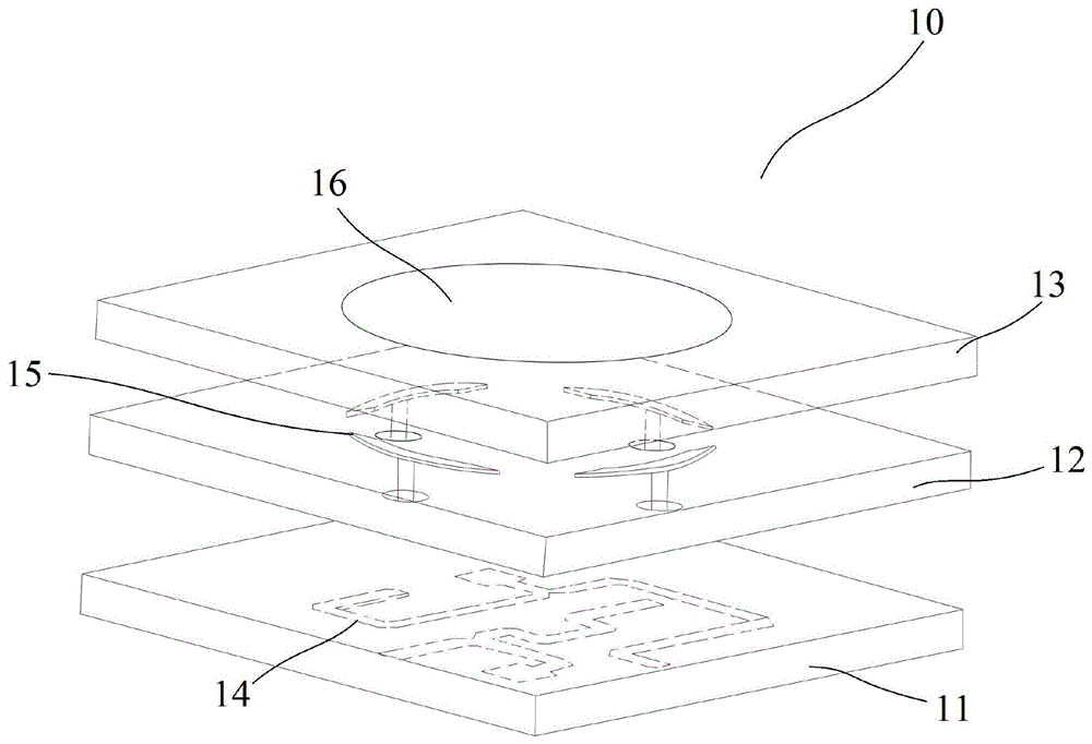
图1示出了本发明实施例提供的一种电子设备的盖体的结构示意图。如图1所示,电子设备的盖体10包括:第一介质层11、设置于第一介质层11的第一表面上的第二介质层12、设置于第二介质层12上的第三介质层13,该第二介质层12设置于第一介质层11和第三介质层13之间。FIG. 1 shows a schematic structural diagram of a cover of an electronic device provided by an embodiment of the present invention. As shown in FIG. 1 , the
本发明实施例中,上述第一介质层11的第二表面上设置有馈电网络14,该第二表面与第一表面相背设置;上述馈电网络14与穿过第二介质层12和第一介质层11的耦合馈电单元15电连接;上述第三介质层13承载有目标辐射体16,该耦合馈电单元15与目标辐射体16耦合连接。In the embodiment of the present invention, a
可以理解,上述第一表面和第二表面为第一介质层11中两个相反方向的表面,即第一表面为第一介质层11中与第二介质层12接触的表面(即朝向第二介质层12的表面),第二表面为第一介质层11中背向第二介质层12的表面。It can be understood that the above-mentioned first surface and second surface are surfaces in two opposite directions in the first
可选的,本发明实施例中,上述第一介质层11、第二介质层12和第三介质层13均可以为介质基板。Optionally, in the embodiment of the present invention, the first
可选的,本发明实施例中,上述第一介质层11、第二介质层12或第三介质层13可以由非金属材料制成;该上述第一介质层11、第二介质层12和第三介质层13具体可以由陶瓷材料制成。Optionally, in this embodiment of the present invention, the first
可选的,在本发明实施例的一种可能的实现方式中,上述耦合馈电单元15包括至少一个馈电部和至少一个馈电臂,每个馈电部分别与一个馈电臂电连接,该至少一个馈电部位于第二介质层12中,该至少一个馈电臂位于第二介质层12的第三表面,该第三表面为第二介质层12中与第三介质层13接触的表面。Optionally, in a possible implementation manner of the embodiment of the present invention, the above-mentioned
需要说明的是,上述“至少一个馈电臂位于第二介质层12的第三表面”可以理解为:至少一个馈电臂中的每个馈电臂的全部部位位于第二介质层12的第三表面;或者,至少一个馈电臂中的每个馈电臂的部分部位位于第二介质层12的第三表面;或者,至少一个馈电臂中的一部分馈电臂的全部部位位于第二介质层12的第三表面。It should be noted that the above-mentioned "at least one feeding arm is located on the third surface of the second
可选的,本发明实施例中,上述至少一个馈电臂为圆弧状馈电臂,该至少一个馈电臂中的每个馈电臂分别朝向目标辐射体16设置。Optionally, in this embodiment of the present invention, the at least one feeder arm is an arc-shaped feeder arm, and each feeder arm of the at least one feeder arm is respectively disposed toward the
需要说明的是,上述“每个馈电臂分别朝向目标辐射体16设置”可以理解为:每个馈电臂的圆弧弧心位于该每个馈电臂的靠近目标辐射体16的一侧。It should be noted that the above "each feeder arm is respectively set towards the
示例性的,如图2所示,耦合馈电单元15包括至少一个馈电部(例如馈电部151、馈电部152、馈电部153和馈电部154)和至少一个馈电臂(例如圆弧状馈电臂155、圆弧状馈电臂156、圆弧状馈电臂157和圆弧状馈电臂158),该馈电部151与圆弧状馈电臂155电连接,该馈电部152与圆弧状馈电臂156电连接,该馈电部153与圆弧状馈电臂157电连接,该馈电部154与圆弧状馈电臂158电连接;该馈电部151、馈电部152、馈电部153和馈电部154位于第二介质层12中,该圆弧状馈电臂155、圆弧状馈电臂156、圆弧状馈电臂157和圆弧状馈电臂158位于第二介质层12的第三表面。Exemplarily, as shown in FIG. 2 , the
可选的,在本发明实施例的另一种可能的实现方式中,上述耦合馈电单元15包括至少一个馈电部和至少一个馈电臂,每个馈电部分别与一个馈电臂电连接,该至少一个馈电部和至少一个馈电臂位于第二介质层12中。Optionally, in another possible implementation manner of the embodiment of the present invention, the above-mentioned
需要说明的是,上述“至少一个馈电臂位于第二介质层12中”可以理解为:至少一个馈电臂中的每个馈电臂的全部部位位于第二介质层12中。It should be noted that “at least one feeding arm is located in the
可选的,本发明实施例中,可以通过圆弧状馈电臂进行圆弧耦合馈电,以使得圆弧状馈电臂可以通过圆弧耦合馈电方式对目标辐射体16耦合馈电,以提升目标辐射体16的带宽,从而满足目标辐射体16对不同网络制式频段的兼容性需求。Optionally, in this embodiment of the present invention, arc coupling feeding may be performed through an arc-shaped feeding arm, so that the arc-shaped feeding arm can couple and feed the
示例性的,图3示出了本发明实施例中的目标辐射体16的反射系数图,如图3所示,通过圆弧耦合馈电方式对目辐射体进行圆弧耦合馈电,以使得目标辐射体16的带宽可以达到-10dB,-10dB带宽可以覆盖23GHz-46GHz的频段,从而可以满足n257-n261的全球主流5G毫米波频段。Exemplarily, FIG. 3 shows a reflection coefficient diagram of the
本发明实施例中,可以通过设置至少一个圆弧状馈电臂,以通过圆弧耦合馈电方式对目标辐射体进行耦合馈电,从而可以提升目标辐射体的带宽。In the embodiment of the present invention, at least one arc-shaped feeding arm can be provided to couple and feed the target radiator by means of circular arc coupling and feeding, so that the bandwidth of the target radiator can be improved.
可选的,本发明实施例中,上述馈电网络14包括至少一个等功分移向网络,每个等功分移向网络的两端分别与不同的馈电臂电连接,且每个等功分移向网络连接的馈电臂均不同。Optionally, in this embodiment of the present invention, the above-mentioned
可选的,本发明实施例中,上述耦合馈电单元15包括的馈电臂的个数与馈电网络14包括的等功分移向网络的端的总个数相同。Optionally, in this embodiment of the present invention, the number of feeding arms included in the
示例性的,结合图2,如图4所示,馈电网络14包括至少一个等功分移向网络(例如等功分移向网络17和等功分移向网络18),该等功分移向网络17的一端(例如V-)与馈电臂155电连接,该等功分移向网络17的另一端(例如V+)与馈电臂157电连接,该等功分移向网络18的一端(H-)与馈电臂156电连接,该等功分移向网络18的另一端(H+)与馈电臂158电连接。Exemplarily, with reference to FIG. 2 and as shown in FIG. 4 , the
可选的,本发明实施例中,可以通过至少一个等功分移向网络使得目标辐射体16辐射信号幅度相等且相位差为180°的差分信号。Optionally, in this embodiment of the present invention, the
可选的,本发明实施例中,在至少一个等功分移向网络包括两个等功分移向网络的情况下,可以通过一个等功分移向网络激励起目标辐射体16辐射的水平方向的信号,可以通过另一个等功分移向网络激励起目标辐射体16辐射的垂直方向的信号,从而实现信号的双极化(即正交极化)。Optionally, in this embodiment of the present invention, in the case where at least one equal-power-division moving network includes two equal-power-division moving networks, the level of radiation of the
本发明实施例中,当至少两个等功分移向网络同时工作时,可以形成多输入多输出(multiple-input multiple-output,MIMO)的多路信号传输方式,从而提升信号的传输速率。In the embodiment of the present invention, when at least two equal-power-division networks work simultaneously, a multiple-input multiple-output (MIMO) multi-channel signal transmission mode can be formed, thereby increasing the signal transmission rate.
本发明实施例,上述馈电网络14与耦合馈电单元15电连接,以通过耦合馈电方式向耦合馈电单元15馈电,从而耦合馈电单元15可以通过耦合馈电方式向目标辐射体16进行耦合馈电,以使得该目标辐射体16产生谐振,从而该目标辐射体16可以辐射信号。In this embodiment of the present invention, the above-mentioned
本发明实施例中,可以通过至少一个等功分移向网络对目标辐射体进行差分馈电,从而可以提升目标辐射体的共模抑制的能力和抗干扰能力,且可以提升差分的端到端的隔离度以及目标辐射体辐射的信号极化的纯度。In the embodiment of the present invention, the target radiator can be differentially fed through at least one equal-power-division moving network, so that the common-mode rejection capability and anti-interference capability of the target radiator can be improved, and the differential end-to-end performance can be improved. Isolation and purity of signal polarization radiated by the target radiator.
需要说明的是,上述“馈电网络14与穿过第二介质层12和第一介质层11的耦合馈电单元15电连接”可以理解为:耦合馈电单元15的一端(即每个馈电部的一端)与第一介质层11的第二表面上设置的馈电网络14电连接,且该耦合馈电单元15的另一端(即每个馈电部的另一端)位于第二介质层12的第三表面。It should be noted that the above-mentioned "the
可选的,本发明实施例中,上述目标辐射体16(或目标辐射单元)可以设置于第三介质层13中或第三介质层13的表面上。Optionally, in this embodiment of the present invention, the above-mentioned target radiator 16 (or target radiation unit) may be disposed in the
可选的,本发明实施例中,上述目标辐射体16可以为毫米波辐射体。Optionally, in this embodiment of the present invention, the above-mentioned
可选的,本发明实施例中,上述目标辐射体16可以包括高频辐射体和低频辐射体中的至少一个。Optionally, in this embodiment of the present invention, the above-mentioned
可以理解,上述盖体10为多层结构,上述第一介质层11、第二介质层12和第三介质层13为该盖体10的层结构。盖体10可以看作为天线单元(例如毫米波天线)。It can be understood that the
可选的,本发明实施例中,上述第二介质层12的第四表面上设置有金属层,该第四表面为第二介质层12中与第一介质层11接触的表面。Optionally, in the embodiment of the present invention, a metal layer is provided on the fourth surface of the
可以理解,上述第三表面和第四表面为第二介质层12中两个相反方向的表面,即第三表面为第二介质层12中与第三介质层13接触的表面(即朝向第三介质层13的表面),第四表面为第二介质层12中朝向第一介质层11的表面。It can be understood that the above-mentioned third surface and fourth surface are surfaces in two opposite directions in the
本发明实施例中,可以通过设置金属层,以降低电子设备中其他器件(例如与馈电网络14连接的器件)对天线单元的影响,从而实现天线单元的边界条件相对固定。In this embodiment of the present invention, a metal layer can be provided to reduce the influence of other devices in the electronic device (eg, devices connected to the feeding network 14 ) on the antenna unit, so that the boundary conditions of the antenna unit are relatively fixed.
本发明实施例提供一种电子设备的盖体,该盖体包括第一介质层、第二介质层和第三介质层,且第一介质层上设置有馈电网络,该馈电网络与穿过第二介质层和第一介质层的耦合馈电单元电连接,第三介质层承载有目标辐射体,耦合馈电单元与目标辐射体耦合连接。由于电子设备的盖体包括多个介质层,该多个介质层设置的各个模块(即馈电网络、耦合馈电单元和目标辐射体)可以构成天线单元(即天线),即该盖体可以看作天线单元,因此可以避免电子设备的盖体对天线单元的覆盖范围的影响,从而可以提高电子设备中的天线单元的性能。An embodiment of the present invention provides a cover body of an electronic device, the cover body includes a first dielectric layer, a second dielectric layer and a third dielectric layer, and a feeding network is provided on the first dielectric layer, and the feeding network is connected with the wear-through network. The second dielectric layer is electrically connected to the coupling feeding unit of the first dielectric layer, the third dielectric layer carries the target radiator, and the coupling feeding unit is coupled and connected to the target radiator. Since the cover of the electronic device includes a plurality of dielectric layers, each module (ie the feeding network, the coupling feeding unit and the target radiator) provided with the multiple dielectric layers can constitute an antenna unit (ie the antenna), that is, the cover can As an antenna unit, the influence of the cover of the electronic device on the coverage of the antenna unit can be avoided, so that the performance of the antenna unit in the electronic device can be improved.
可选的,本发明实施例中,电子设备的盖体10可以包括至少一个天线模组,每个天线模组包括第一介质层11、第二介质层12和第三介质层13。Optionally, in this embodiment of the present invention, the
需要说明的是,盖体10包括的天线模组的数量和天线模组的位置可以根据实际使用需求设定,本发明实施例对此不作限制。It should be noted that, the number of antenna modules included in the
可以理解,本发明实施例在盖体10上集成毫米波天线(即毫米波阵列天线),可以较大程度的减少周围环境以及用户手握的影响,使得毫米波天线的性能大幅提升。It can be understood that the embodiment of the present invention integrates a millimeter-wave antenna (ie, a millimeter-wave array antenna) on the
可选的,本发明实施例中,上述第三介质层13包括相互平行设置的至少一个第一子介质层,上述目标辐射体16包括每个第一子介质层承载的子辐射体。Optionally, in the embodiment of the present invention, the
可选的,本发明实施例中,每个第一子介质层中分别设置有一个子辐射体,或者,每个第一子介质层的第五表面上分别设置有一个子辐射体,一个第五表面为一个第一子介质层中背向第二介质层12的表面。Optionally, in this embodiment of the present invention, each first sub-dielectric layer is provided with a sub-radiator respectively, or, a sub-radiator is respectively provided on the fifth surface of each first sub-dielectric layer, and a first sub-radiator is provided on the fifth surface of each first sub-dielectric layer. The fifth surface is the surface of a first sub-dielectric layer facing away from the
可选的,本发明实施例中,每个第一子介质层承载的子辐射体可以为毫米波辐射体,该子辐射体可以为高频辐射体或低频辐射体。Optionally, in this embodiment of the present invention, the sub-radiator carried by each first sub-dielectric layer may be a millimeter wave radiator, and the sub-radiator may be a high-frequency radiator or a low-frequency radiator.
可选的,本发明实施例中,上述子辐射体的形状可以为以下任一项:圆形、椭圆形、三角形、正方形、矩形、菱形和多边形。具体的,可以根据实际使用需求设定,本发明实施例中不作限制。Optionally, in this embodiment of the present invention, the shape of the sub-radiator may be any one of the following: a circle, an ellipse, a triangle, a square, a rectangle, a rhombus, and a polygon. Specifically, it can be set according to actual usage requirements, which is not limited in the embodiment of the present invention.
可选的,本发明实施例中,上述至少一个第一子介质层中,与第二介质层12接触的第一子介质层承载的子辐射体与耦合馈电单元15耦合连接;且每个第一子介质层承载的子辐射体中任意两个相邻的子辐射体耦合连接。Optionally, in this embodiment of the present invention, in the at least one first sub-dielectric layer, the sub-radiator carried by the first sub-dielectric layer in contact with the
可以理解,可以通过耦合馈电单元15向直接与该耦合馈电单元15耦合连接的子辐射体(即至少一个第一子介质层中与第二介质层12接触的第一子介质层承载的子辐射体)馈电,然后再通过该子辐射体向与该子辐射体耦合连接的子辐射体耦合馈电,以此类推,直至完成向所有第一子介质层承载的子辐射体馈电。It can be understood that the sub-radiators directly coupled and connected to the coupling feeding unit 15 (that is, the radiators carried by the first sub-dielectric layer in contact with the
需要说明的是,子辐射体向与该子辐射体耦合连接的子辐射体耦合馈电可以理解为:子辐射体通过辐射信号,以使得与该子辐射体耦合连接的子辐射体产生谐振,从而也辐射信号。It should be noted that the coupling feeding of the sub-radiator to the sub-radiator coupled to the sub-radiator can be understood as: the sub-radiator passes the radiation signal, so that the sub-radiator coupled to the sub-radiator resonates, Thereby the signal is also radiated.
可选的,本发明实施例中,任意两个相邻的子辐射体是相对设置的。Optionally, in this embodiment of the present invention, any two adjacent sub-radiators are disposed opposite to each other.
需要说明的是,上述“任意两个相邻的子辐射体是相对设置的”可以理解为:一个子辐射体的中心点与另一个子辐射体的中心点的连线,垂直于一个第一子介质层所在平面。It should be noted that the above-mentioned "any two adjacent sub-radiators are set opposite to each other" can be understood as: the line connecting the center point of one sub-radiator and the center point of the other sub-radiator is perpendicular to a first The plane where the sub-dielectric layer is located.
示例性的,结合图1,如图5所示,第三介质层13包括相互平行设置的至少一个第一子介质层(例如介质层17和介质层18),该介质层17的一个表面与第二介质层12接触,该介质层17的另一个表面设置有子辐射体19,且该介质层17的另一个表面与介质层18的一个表面接触,该介质层18的另一表面设置有子辐射体20;该子辐射体19与耦合馈电单元15耦合连接,该子辐射体19与该子辐射体20相对设置,且该子辐射体19与该子辐射体20耦合连接。Exemplarily, with reference to FIG. 1 , as shown in FIG. 5 , the
可选的,本发明实施例中,上述盖体10还可以包括至少一个寄生单元,每个寄生单元均贯穿至少一个第一子介质层设置。Optionally, in this embodiment of the present invention, the
可选的,本发明实施例中,上述至少一个寄生单元中的每个寄生单元均为金属过孔结构。Optionally, in this embodiment of the present invention, each parasitic unit in the at least one parasitic unit is a metal via structure.
可以理解,上述金属过孔结构为空心圆柱结构。It can be understood that the above-mentioned metal via structure is a hollow cylindrical structure.
可选的,本发明实施例中,在任意一个第一子介质层中,上述至少一个寄生单元分布在该任意一个第一子介质层承载的子辐射体的周围。Optionally, in this embodiment of the present invention, in any one of the first sub-dielectric layers, the at least one parasitic unit described above is distributed around the sub-radiators carried by the any one of the first sub-dielectric layers.
可选的,本发明实施例中,上述至少一个寄生单元均匀分布在第一子介质层承载的子辐射体的周围。Optionally, in this embodiment of the present invention, the above-mentioned at least one parasitic unit is uniformly distributed around the sub-radiators carried by the first sub-dielectric layer.
示例性的,结合图5,如图6所示,上述盖体10还包括至少一个寄生单元(例如寄生单元a、寄生单元b、寄生单元c、寄生单元d、寄生单元e、寄生单元f、寄生单元g和寄生单元h),该至少一个寄生单元中每个寄生单元均贯穿至少一个第一子介质层(例如介质层17和介质层18)设置,且至少一个寄生单元均匀分布在子辐射体19和子辐射体20的周围。Exemplarily, with reference to FIG. 5 , as shown in FIG. 6 , the above-mentioned
本发明实施例中,在每个子辐射体辐射信号的情况下,每个寄生单元均可以产生谐振,从而可以拓宽每个子辐射体的辐射方向图的波束宽度,进而可以增加阵列扫描的覆盖角度。In the embodiment of the present invention, when each sub-radiator radiates a signal, each parasitic unit can generate resonance, so that the beam width of the radiation pattern of each sub-radiator can be widened, thereby increasing the coverage angle of the array scanning.
示例性的,图7示出了本发明实施例提供的目标辐射体16辐射的信号的仿真方向图。如图7所示,目标辐射体16辐射的信号对应的波束的宽度为3dB,在设置至少一个寄生单元之前,该宽度为3dB的波束对应的信号的覆盖角度D=78.2度,在设置至少一个寄生单元之后,该宽度为3dB的波束对应的信号的覆盖角度增加至D1=100.6度。Exemplarily, FIG. 7 shows a simulation pattern of a signal radiated by the
本发明实施例中,可以通过至少一个寄生单元贯穿至少一个第一子介质层设置,以拓宽至少一个第一子介质层承载的子辐射体的辐射方向图的波束宽度,从而可以增加阵列扫描的覆盖角度,以增加这些子辐射体的辐射覆盖范围。In this embodiment of the present invention, at least one parasitic unit may be disposed through at least one first sub-dielectric layer to widen the beam width of the radiation pattern of the sub-radiators carried by the at least one first sub-dielectric layer, thereby increasing the scanning efficiency of the array. coverage angle to increase the radiation coverage of these sub-radiators.
可以理解,通过耦合方式用以提升天线单元的带宽,同时天线单元周围的至少一个寄生单元拓宽了天线的波束宽度,从而实现更好的波束扫描特性。It can be understood that the coupling method is used to increase the bandwidth of the antenna unit, and at the same time at least one parasitic unit around the antenna unit widens the beam width of the antenna, thereby achieving better beam scanning characteristics.
可选的,本发明实施例中,上述第三介质层13还包括相互平行设置的至少一个第二子介质层,任意第二子介质层与第一子介质层相互平行设置;该至少一个第二子介质层上设置有至少一个寄生单元,该至少一个寄生单元贯穿至少一个第二子介质层。Optionally, in this embodiment of the present invention, the
可以理解,至少一个第一子介质层中每个第一子介质层分别承载有一个子辐射体,至少一个第二子介质层中每个第二子介质层上分别设置有至少一个寄生单元。It can be understood that each of the at least one first sub-dielectric layer carries a sub-radiator respectively, and each of the at least one second sub-dielectric layer is respectively provided with at least one parasitic unit.
可选的,本发明实施例中,上述至少一个第一子介质层中的一个第一子介质层与第二介质层12的第三表面接触,且至少一个第二子介质层中的一个第二子介质层与至少一个第一子介质层中的另一个第一子介质层(即至少一个第一子介质层中距离该一个第一子介质层最远的第一子介质层)接触。Optionally, in this embodiment of the present invention, one of the at least one first sub-dielectric layer is in contact with the third surface of the
示例性的,结合图1,如图8所示,第三介质层13包括相互平行设置的至少一个第一子介质层(例如介质层21)和相互平行设置的至少一个第二子介质层(例如介质层22),介质层21与介质层22相互平行设置;该介质层21的一个表面与第二介质层12接触,该介质层21的另一个表面设置有子辐射体23,且该介质层21的另一个表面与介质层22的一个表面接触,该介质层22上设置有至少一个寄生单元(例如寄生单元a、寄生单元b、寄生单元c和寄生单元d)。Exemplarily, with reference to FIG. 1 , as shown in FIG. 8 , the
可选的,本发明实施例中,上述至少一个第二子介质层中的一个第二子介质层与第二介质层12的第三表面接触,且至少一个第一子介质层中的一个第一子介质层与至少一个第二子介质层中的另一个第二子介质层(即至少一个第二子介质层中距离该一个第二子介质层最远的第二子介质层)接触。Optionally, in this embodiment of the present invention, one second sub-dielectric layer in the at least one second sub-dielectric layer is in contact with the third surface of the
本发明实施例中,可以通过至少一个寄生单元贯穿至少一个第二子介质层设置,以拓宽至少一个第一子介质层承载的子辐射体的辐射方向图的波束宽度,从而可以增加阵列扫描的覆盖角度,以增加这些子辐射体的辐射覆盖范围。In this embodiment of the present invention, at least one parasitic unit may be disposed through at least one second sub-dielectric layer to widen the beam width of the radiation pattern of the sub-radiators carried by the at least one first sub-dielectric layer, thereby increasing the scanning efficiency of the array. coverage angle to increase the radiation coverage of these sub-radiators.
可选的,本发明实施例中,上述馈电网络14与电子设备中的信号处理模块贴合电连接,或者,上述馈电网络14通过信号传输线与电子设备中的信号处理模块电连接。Optionally, in the embodiment of the present invention, the above-mentioned
可选的,本发明实施例中,上述信号处理模块可以为IC芯片,该IC芯片可以包括PMIC和RFIC。Optionally, in this embodiment of the present invention, the above-mentioned signal processing module may be an IC chip, and the IC chip may include a PMIC and an RFIC.
可选的,本发明实施例中,上述馈电网络14与RFIC贴合电连接,该PMIC通过连接器与电子设备中的处理器电连接。Optionally, in the embodiment of the present invention, the above-mentioned
可选的,本发明实施例中,上述馈电网络14与RFIC通过信号传输线与RFIC电连接,该PMIC通过连接器与电子设备中的处理器电连接。Optionally, in this embodiment of the present invention, the
可选的,本发明实施例中,上述信号传输线可以为以下任一项:衬底集成波导(substrate integratedwaveguide,SIW)和微带线。Optionally, in this embodiment of the present invention, the above signal transmission line may be any one of the following: a substrate integrated waveguide (SIW) and a microstrip line.
可选的,本发明实施例中,可以将盖体10和信号处理模块看作天线系统。Optionally, in this embodiment of the present invention, the
示例性的,图9A示出了本发明实施例提供的盖体10的天线模组的布局示意图。如图9A所示,盖体10包括至少一个天线模块(例如天线模组X、天线模块Y和天线模组Z),且天线模组X、天线模块Y和天线模组Z位于盖体10的不同位置。Exemplarily, FIG. 9A shows a schematic layout diagram of the antenna module of the
示例性的,以盖体10包括一个天线模组为例进行示意。图9B示出了本发明实施例提供的盖体10的剖视图,如图9B所示,该盖体10包括第一介质层11、第二介质层12和相互平行设置的至少一个第一子介质层(例如介质层17和介质层18),该第一介质层11上设置有馈电网络14,该馈电网络14与穿过第二介质层12和第一介质层11的耦合馈电单元15电连接,该介质层17上设置有子辐射体19,该介质层18上设置有子辐射体20,至少一个寄生单元24贯穿介质层17和介质层18设置,该馈电网络14与信号处理模块25(例如PMIC和RFIC)贴合电连接。Illustratively, the
又示例性的,图9C示出了本发明实施例提供的盖体10的剖视图,如图9C所示,该盖体10包括第一介质层11、第二介质层12和至少一个第一子介质层(例如介质层17和介质层18),该第一介质层11上设置有馈电网络14,该馈电网络14与穿过第二介质层12和第一介质层11的耦合馈电单元15电连接,该介质层17上设置有子辐射体19,该介质层18上设置有子辐射体20,至少一个寄生单元24贯穿介质层17和介质层18设置,馈电网络14与电子设备中的信号处理模块25通过信号传输线26电连接。For another example, FIG. 9C shows a cross-sectional view of a
可以理解,可以通过信号传输线将馈电网络14与信号处理模块连接,从而盖体10(即天线单元)与信号处理模块在空间位置上可以错开,以减少整机堆叠的难度,并且可以拓宽天线单元布局的自由度,可以选择天线单元最优的布局位置,且不对其他器件造成影响。It can be understood that the
可选的,本发明实施例中,可以通过低温共烧陶瓷(low temperature co-firedceramic,LTCC)工艺制作盖体10,并将盖体10与信号处理模块贴合设置。Optionally, in the embodiment of the present invention, the
示例性的,如图10A所示,可以通过LTCC工艺将盖体10的第一介质层11、第二介质层12、第三介质层13、馈电网络14、耦合馈电单元15和目标辐射体16制作成型;如图10B所示,可以将通过LTCC工艺制作成型的盖体10与信号处理模块25通过倒装焊工艺焊接;如图10C所示,可以将与信号处理模块25焊接的盖体10通过计算机数控(computer numericalcontrol,CNC)工艺铣出所需的外形;如图10D所示,可以对通过CNC工艺的盖体10进行彩色材料(color material finish,CMF)表面处理,形成彩色涂层27,以完成盖体10的制作。Exemplarily, as shown in FIG. 10A , the
可以理解,本发明实施例可以利用LTCC工艺将毫米波天线单元与盖体10集成,形成天线单元即盖体10的结构关系,在解决盖体10对于天线单元性能影响的同时,节省了天线单元所需的空间,以提升产品的竞争力。It can be understood that in this embodiment of the present invention, the millimeter-wave antenna unit and the
可选的,本发明实施例中,盖体10(即天线单元)可以应用于无线广域网络(wireless wide area network,WWAN)、无线区域网络(wireless local area networks,WLAN)、射频识别(radio frequency identification,RFID)、近场通信(near fieldcommunication,NFC)或无线充电等。Optionally, in this embodiment of the present invention, the cover 10 (ie, the antenna unit) may be applied to a wireless wide area network (WWAN), a wireless local area network (WLAN), a radio frequency identification (radio frequency) identification, RFID), near field communication (near field communication, NFC) or wireless charging, etc.
图11示出了本发明实施例中涉及的电子设备的一种可能的结构示意图。如图11所示,电子设备50可以包括:上述实施例中的盖体10。FIG. 11 shows a possible schematic structural diagram of the electronic device involved in the embodiment of the present invention. As shown in FIG. 11 , the
可选的,本发明实施例中,上述电子设备可以为移动电子设备,也可以为非移动电子设备。示例性的,移动电子设备可以为手机、平板电脑、笔记本电脑、掌上电脑、车载电子设备、可穿戴设备、超级移动个人计算机(ultra-mobile personal computer,UMPC)、上网本、个人游戏机、智能手表、电子摄像设备或者个人数字助理(personal digitalassistant,PDA)等,非移动电子设备可以为个人计算机(personal computer,PC)、电视机(television,TV)、柜员机或者自助机等,本发明实施例不作具体限定。Optionally, in this embodiment of the present invention, the foregoing electronic device may be a mobile electronic device or a non-mobile electronic device. Exemplarily, the mobile electronic device may be a mobile phone, a tablet computer, a notebook computer, a palmtop computer, an in-vehicle electronic device, a wearable device, an ultra-mobile personal computer (UMPC), a netbook, a personal game console, a smart watch , electronic camera equipment or personal digital assistant (personal digital assistant, PDA), etc., the non-mobile electronic equipment can be a personal computer (personal computer, PC), television (television, TV), teller machine or self-service machine, etc. Specific restrictions.
可选的,本发明实施例中,电子设备还可以包括信号处理模块,盖体10中的馈电网络14与信号处理模块连接(例如贴合电连接或通过信号传输线连接)。Optionally, in this embodiment of the present invention, the electronic device may further include a signal processing module, and the
本发明实施例提供一种电子设备,该电子设备包括盖体,由于该盖体包括多个介质层,该多个介质层设置的各个模块(即馈电网络、耦合馈电单元和目标辐射体)构成天线单元(即天线),即该盖体可以看作天线单元,因此可以避免电子设备的盖体对天线单元的覆盖范围的影响,从而可以提高电子设备中的天线单元的性能。An embodiment of the present invention provides an electronic device, which includes a cover. Since the cover includes a plurality of dielectric layers, each module (ie, a feeding network, a coupling feeding unit, and a target radiator) provided with the plurality of dielectric layers ) constitutes an antenna unit (ie, an antenna), that is, the cover can be regarded as an antenna unit, so the influence of the cover of the electronic device on the coverage of the antenna unit can be avoided, thereby improving the performance of the antenna unit in the electronic device.
需要说明的是,在本文中,术语“包括”、“包含”或者其任何其他变体意在涵盖非排他性的包含,从而使得包括一系列要素的过程、方法、物品或者装置不仅包括那些要素,而且还包括没有明确列出的其他要素,或者是还包括为这种过程、方法、物品或者装置所固有的要素。在没有更多限制的情况下,由语句“包括一个……”限定的要素,并不排除在包括该要素的过程、方法、物品或者装置中还存在另外的相同要素。It should be noted that, herein, the terms "comprising", "comprising" or any other variation thereof are intended to encompass non-exclusive inclusion, such that a process, method, article or device comprising a series of elements includes not only those elements, It also includes other elements not expressly listed or inherent to such a process, method, article or apparatus. Without further limitation, an element qualified by the phrase "comprising a..." does not preclude the presence of additional identical elements in a process, method, article or apparatus that includes the element.
通过以上的实施方式的描述,本领域的技术人员可以清楚地了解到上述实施例方法可借助软件加必需的通用硬件平台的方式来实现,当然也可以通过硬件,但很多情况下前者是更佳的实施方式。基于这样的理解,本发明的技术方案本质上或者说对现有技术做出贡献的部分可以以软件产品的形式体现出来,该计算机软件产品存储在一个存储介质(如ROM/RAM、磁碟、光盘)中,包括若干指令用以使得一台电子设备(可以是手机,计算机,服务器,空调器,或者网络设备等)执行本发明各个实施例所述的方法。From the description of the above embodiments, those skilled in the art can clearly understand that the method of the above embodiment can be implemented by means of software plus a necessary general hardware platform, and of course can also be implemented by hardware, but in many cases the former is better implementation. Based on this understanding, the technical solutions of the present invention can be embodied in the form of software products in essence or the parts that make contributions to the prior art, and the computer software products are stored in a storage medium (such as ROM/RAM, magnetic disk, CD-ROM), including several instructions to make an electronic device (which may be a mobile phone, a computer, a server, an air conditioner, or a network device, etc.) to execute the methods described in the various embodiments of the present invention.
上面结合附图对本发明的实施例进行了描述,但是本发明并不局限于上述的具体实施方式,上述的具体实施方式仅仅是示意性的,而不是限制性的,本领域的普通技术人员在本发明的启示下,在不脱离本发明宗旨和权利要求所保护的范围情况下,还可做出很多形式,均属于本发明的保护之内。The embodiments of the present invention have been described above in conjunction with the accompanying drawings, but the present invention is not limited to the above-mentioned specific embodiments, which are merely illustrative rather than restrictive. Under the inspiration of the present invention, without departing from the spirit of the present invention and the scope protected by the claims, many forms can be made, which all belong to the protection of the present invention.
Claims (12)
Priority Applications (1)
| Application Number | Priority Date | Filing Date | Title |
|---|---|---|---|
| CN202010208293.8A CN111403912B (en) | 2020-03-23 | 2020-03-23 | Electronic equipment's lid and electronic equipment |
Applications Claiming Priority (1)
| Application Number | Priority Date | Filing Date | Title |
|---|---|---|---|
| CN202010208293.8A CN111403912B (en) | 2020-03-23 | 2020-03-23 | Electronic equipment's lid and electronic equipment |
Publications (2)
| Publication Number | Publication Date |
|---|---|
| CN111403912A true CN111403912A (en) | 2020-07-10 |
| CN111403912B CN111403912B (en) | 2022-09-30 |
Family
ID=71429096
Family Applications (1)
| Application Number | Title | Priority Date | Filing Date |
|---|---|---|---|
| CN202010208293.8A Active CN111403912B (en) | 2020-03-23 | 2020-03-23 | Electronic equipment's lid and electronic equipment |
Country Status (1)
| Country | Link |
|---|---|
| CN (1) | CN111403912B (en) |
Cited By (1)
| Publication number | Priority date | Publication date | Assignee | Title |
|---|---|---|---|---|
| TWI830381B (en) * | 2022-09-14 | 2024-01-21 | 泓博無線通訊技術有限公司 | Millimeter wave antenna for dual-polarized operation |
Citations (5)
| Publication number | Priority date | Publication date | Assignee | Title |
|---|---|---|---|---|
| US20080129624A1 (en) * | 2003-03-06 | 2008-06-05 | Raysat Cyprus Limited | Flat Mobile Antenna System |
| CN102686060A (en) * | 2012-05-23 | 2012-09-19 | 上海华勤通讯技术有限公司 | Housing of mobile terminal and manufacturing method as well as mobile terminal thereof |
| CN105514584A (en) * | 2016-01-18 | 2016-04-20 | 西安爱生技术集团公司 | A Vertically Polarized C-Band Broadband Short Backfiring Antenna |
| CN106785408A (en) * | 2017-01-24 | 2017-05-31 | 桂林电子科技大学 | Broadband low section omnidirectional circular-polarized antenna |
| CN210040532U (en) * | 2019-06-25 | 2020-02-07 | 广东盛路通信科技股份有限公司 | Broadband navigation antenna |
-
2020
- 2020-03-23 CN CN202010208293.8A patent/CN111403912B/en active Active
Patent Citations (5)
| Publication number | Priority date | Publication date | Assignee | Title |
|---|---|---|---|---|
| US20080129624A1 (en) * | 2003-03-06 | 2008-06-05 | Raysat Cyprus Limited | Flat Mobile Antenna System |
| CN102686060A (en) * | 2012-05-23 | 2012-09-19 | 上海华勤通讯技术有限公司 | Housing of mobile terminal and manufacturing method as well as mobile terminal thereof |
| CN105514584A (en) * | 2016-01-18 | 2016-04-20 | 西安爱生技术集团公司 | A Vertically Polarized C-Band Broadband Short Backfiring Antenna |
| CN106785408A (en) * | 2017-01-24 | 2017-05-31 | 桂林电子科技大学 | Broadband low section omnidirectional circular-polarized antenna |
| CN210040532U (en) * | 2019-06-25 | 2020-02-07 | 广东盛路通信科技股份有限公司 | Broadband navigation antenna |
Cited By (1)
| Publication number | Priority date | Publication date | Assignee | Title |
|---|---|---|---|---|
| TWI830381B (en) * | 2022-09-14 | 2024-01-21 | 泓博無線通訊技術有限公司 | Millimeter wave antenna for dual-polarized operation |
Also Published As
| Publication number | Publication date |
|---|---|
| CN111403912B (en) | 2022-09-30 |
Similar Documents
| Publication | Publication Date | Title |
|---|---|---|
| US11973280B2 (en) | Antenna element and terminal device | |
| US10727580B2 (en) | Millimeter wave antennas having isolated feeds | |
| JP7239743B2 (en) | Antenna unit and terminal equipment | |
| US7701395B2 (en) | Increasing isolation between multiple antennas with a grounded meander line structure | |
| EP3975332B1 (en) | Antenna unit and terminal device | |
| US10763589B2 (en) | Millimeter wave patch antennas with parasitic elements | |
| WO2018028162A1 (en) | Decoupling assembly, multi-antenna system and terminal | |
| CN110474158A (en) | A kind of antenna element and terminal device | |
| EP3852194B1 (en) | Terminal device antenna | |
| WO2021104191A1 (en) | Antenna unit and electronic device | |
| CN112993592A (en) | Antenna packaging module and electronic equipment | |
| CN110828985A (en) | Antenna unit and electronic equipment | |
| KR102848207B1 (en) | Antenna module and electronic device with the same | |
| CN110518340B (en) | Antenna unit and terminal equipment | |
| CN113594687A (en) | Antenna module and electronic equipment | |
| CN110828987A (en) | An antenna unit and electronic equipment | |
| CN111403912A (en) | Electronic equipment's lid and electronic equipment | |
| CN111969304B (en) | Antenna structure and electronic equipment | |
| CN110808455B (en) | Antenna unit and electronic equipment | |
| CN110808454A (en) | An antenna unit and electronic equipment | |
| EP3425731B1 (en) | Antenna assembly and remote control having same | |
| CN110829021A (en) | An antenna unit and electronic equipment | |
| CN110828986A (en) | Antenna unit and electronic equipment | |
| CN210576433U (en) | An antenna unit and electronic equipment | |
| CN110808453A (en) | An antenna unit and electronic equipment |
Legal Events
| Date | Code | Title | Description |
|---|---|---|---|
| PB01 | Publication | ||
| PB01 | Publication | ||
| SE01 | Entry into force of request for substantive examination | ||
| SE01 | Entry into force of request for substantive examination | ||
| GR01 | Patent grant | ||
| GR01 | Patent grant |